JP2011192724A - Composite transformer module - Google Patents
Composite transformer module Download PDFInfo
- Publication number
- JP2011192724A JP2011192724A JP2010055996A JP2010055996A JP2011192724A JP 2011192724 A JP2011192724 A JP 2011192724A JP 2010055996 A JP2010055996 A JP 2010055996A JP 2010055996 A JP2010055996 A JP 2010055996A JP 2011192724 A JP2011192724 A JP 2011192724A
- Authority
- JP
- Japan
- Prior art keywords
- primary
- coil
- power supply
- transformer
- signal
- Prior art date
- Legal status (The legal status is an assumption and is not a legal conclusion. Google has not performed a legal analysis and makes no representation as to the accuracy of the status listed.)
- Pending
Links
Images


Landscapes
- Dc-Dc Converters (AREA)
Abstract
Description
本発明は、電力伝送トランス部及び信号伝送トランス部を備えたトランスと、信号処理回路部とがモジュールとして一体形成された、複合トランスモジュールに関するものである。 The present invention relates to a composite transformer module in which a transformer including a power transmission transformer unit and a signal transmission transformer unit and a signal processing circuit unit are integrally formed as a module.
多層基板に形成された導体パターンをコイルとするトランスと、スイッチング電源回路とが一体化されたスイッチング電源モジュールが特許文献1に開示されている。 A switching power supply module in which a transformer having a conductor pattern formed on a multilayer substrate as a coil and a switching power supply circuit are integrated is disclosed in Patent Document 1.
図1(A)は、特許文献1に関するスイッチング電源モジュールの一例を示す図である。このスイッチング電源モジュール1は、その回路基板2にスイッチング電源回路3が構成されている。スイッチング電源回路3は、トランス4と複数の回路構成部品5と、回路基板2に形成された配線パターン(不図示)とで構成されている。回路構成部品5は、ICチップ、コンデンサ素子、スイッチング素子、整流素子等である。その他に、このスイッチング電源モジュール1をマザーボードに接続するための接続用端子6が設けられている。 FIG. 1A is a diagram illustrating an example of a switching power supply module related to Patent Document 1. FIG. In the switching power supply module 1, a switching power supply circuit 3 is configured on the circuit board 2. The switching power supply circuit 3 includes a transformer 4, a plurality of circuit components 5, and a wiring pattern (not shown) formed on the circuit board 2. The circuit component 5 is an IC chip, a capacitor element, a switching element, a rectifying element, or the like. In addition, a connection terminal 6 for connecting the switching power supply module 1 to the motherboard is provided.
トランス4は、回路基板2に形成されたコイルパターン7と、1対のコア8とで構成されている。回路基板2は複数の導体層が積層形成された積層体であり、1次コイルとなるコイルパターン及び2次コイルとなるコイルパターンが回路基板2に形成され、それら複数のコイルパターンがほぼ同軸関係に積層されている。 The transformer 4 includes a coil pattern 7 formed on the circuit board 2 and a pair of cores 8. The circuit board 2 is a laminated body in which a plurality of conductor layers are laminated. A coil pattern to be a primary coil and a coil pattern to be a secondary coil are formed on the circuit board 2, and the plurality of coil patterns are substantially coaxially related. Are stacked.
回路基板2のコイルパターン7の形成領域にはコア脚挿通孔9が開けられている。コア8のコア脚がコア脚挿通孔9に挿入され、1対のコア8が組み合わされて、コイルパターン7に装着されている。図1に示すように、それら1対のコア8は、コイルパターン7の一部分を回路基板2の表裏両側から挟み込む形で装着されている。 A core leg insertion hole 9 is formed in the formation area of the coil pattern 7 on the circuit board 2. The core leg of the core 8 is inserted into the core leg insertion hole 9, and the pair of cores 8 are combined and attached to the coil pattern 7. As shown in FIG. 1, the pair of cores 8 are mounted such that a part of the coil pattern 7 is sandwiched from both the front and back sides of the circuit board 2.
多層基板に形成された導体パターンをコイルとするトランスと、スイッチング電源回路とが一体化されたスイッチング電源モジュール1には次に述べるような問題がある。 The switching power supply module 1 in which the transformer having the conductor pattern formed on the multilayer substrate as a coil and the switching power supply circuit are integrated has the following problems.
(a)トランス4のコイルパターン7における直流抵抗、交流抵抗を低減し、コイルの導通損失を低減するには、回路基板の積層数を多くする必要がある。トランスの1次−2次間の結合度を強くする上でも、多層基板の積層数を増してサンドイッチ構造にすることが有効である。一方、多層基板の積層数を増すと、それにほぼ比例して基板のコストも増加する。コイルパターン7の内層は、コイルパターンを形成するのに使用されているが、回路構成部品5が実装された直下の内層は必ずしも有効利用できない。特に、大型の回路構成部品を多く必要とするスイッチング電源回路では、スイッチング電源回路全体を高価な多層基板に実装することは、コスト削減の観点からは非効率的である。 (A) In order to reduce the direct current resistance and alternating current resistance in the coil pattern 7 of the transformer 4 and reduce the conduction loss of the coil, it is necessary to increase the number of laminated circuit boards. In order to increase the degree of coupling between the primary and secondary sides of the transformer, it is effective to increase the number of multilayer substrates to form a sandwich structure. On the other hand, when the number of multilayer substrates is increased, the cost of the substrate increases in proportion to it. The inner layer of the coil pattern 7 is used to form the coil pattern, but the inner layer directly below the circuit component 5 is not necessarily effectively used. In particular, in a switching power supply circuit that requires many large circuit components, mounting the entire switching power supply circuit on an expensive multilayer board is inefficient from the viewpoint of cost reduction.
(b)一体型スイッチング電源モジュール1に実装された回路構成部品5のマザーボードに対する熱抵抗が大きいので、回路構成部品5の放熱性に問題が生じる場合がある。一体型スイッチング電源モジュール1が部品の発熱を、主にマザーボードに放熱する構造の場合、伝熱経路としては、回路基板2から接続用端子6を介してマザーボードへ放熱する経路が支配的である。しかし、この一体型スイッチング電源モジュール1を構成する回路基板2の基材は熱抵抗が比較的大きく、回路構成部品5とマザーボードとの伝熱経路の距離も長いことから、回路構成部品5の放熱性が悪い。特に、この一体型スイッチング電源モジュール1が扱う電力が大きい場合には、トランスのコイルパターン7やスイッチング素子などの回路構成部品5の発熱が非常に大きくなり、一体型スイッチング電源モジュール1の効率が低下したり、一体型スイッチング電源モジュール1の使用温度範囲を狭めたりすることになる。 (B) Since the thermal resistance of the circuit component 5 mounted on the integrated switching power supply module 1 to the motherboard is large, there may be a problem in the heat dissipation of the circuit component 5. In the case where the integrated switching power supply module 1 has a structure in which the heat generated from the components is mainly dissipated to the mother board, the heat dissipating path is predominantly a path from the circuit board 2 to the mother board via the connection terminals 6. However, since the base material of the circuit board 2 constituting the integrated switching power supply module 1 has a relatively large thermal resistance and the distance of the heat transfer path between the circuit component 5 and the motherboard is long, the heat dissipation of the circuit component 5 The nature is bad. In particular, when the power handled by the integrated switching power supply module 1 is large, the heat generation of the circuit component 5 such as the transformer coil pattern 7 and the switching element becomes very large, and the efficiency of the integrated switching power supply module 1 is reduced. Or the operating temperature range of the integrated switching power supply module 1 is narrowed.
(c)一体型スイッチング電源モジュール1の回路基板2を構成する多層基板では、各両面基板間の絶縁部分に一定値以上の厚さのプリプレグを挟んで積層しないと、絶縁部分にボイドが生じて信頼性が確保できない。そのため、コイルパターン7を形成する導体層の厚さに対する絶縁層の厚さの比率を大きくする必要がある。トランスコイルの直流抵抗を低減するには、コアの窓枠の中に、コイル導体部が占める比率(占積率)を高くする必要があるが、多層基板で形成したプリントコイルは、薄型構造であるため表皮効果の影響が小さく高周波のスイッチング動作において導通損失を低減できる利点があるものの、前述の理由により、巻線で形成したコイルより占積率が劣る傾向があり、コイルの直流抵抗を十分に低くできないという問題がある。 (C) In the multilayer board constituting the circuit board 2 of the integrated switching power supply module 1, if the prepreg having a thickness of a certain value or more is not sandwiched between the insulating parts between the double-sided boards, voids are generated in the insulating parts. Reliability cannot be secured. Therefore, it is necessary to increase the ratio of the thickness of the insulating layer to the thickness of the conductor layer forming the coil pattern 7. In order to reduce the DC resistance of the transformer coil, it is necessary to increase the ratio (space factor) of the coil conductor part in the core window frame. However, the printed coil formed of a multilayer substrate has a thin structure. However, the effect of the skin effect is small, and there is an advantage that conduction loss can be reduced in high-frequency switching operations. There is a problem that it cannot be lowered.
(d)更に、多層基板に導体パターンで形成した積層コイルから成るトランスでは、基板の信頼性を確保するための最小パターン幅及び最小パターン間隔が規定され、かつ、積層数が多層基板のコストに大きく影響することから、巻き数の極端に多い(例えば100ターン以上の)コイルを形成することが難しい。このため、昇圧比又は降圧比が極端に大きいスイッチング電源では、基板の導体パターンでコイルを形成するプリントコイルでトランスを形成することは困難である。 (D) Further, in a transformer composed of a laminated coil formed with a conductor pattern on a multilayer board, a minimum pattern width and a minimum pattern interval for ensuring the reliability of the board are specified, and the number of layers is reduced to the cost of the multilayer board. Since it greatly affects, it is difficult to form a coil having an extremely large number of turns (for example, 100 turns or more). For this reason, in a switching power supply with an extremely large step-up ratio or step-down ratio, it is difficult to form a transformer with a printed coil that forms a coil with a conductor pattern on a substrate.
(e)トランスの特性に関しては、次に述べる問題がある。図1(B)はトランスの巻線構造の一例を示す断面図である。一般的に、図1(B)のような1次コイル巻線10と2次コイル巻線11を繰り返し積層した構造のトランスでは、各巻線間に図1(B)に示す寄生容量Csが生じる。この各巻線間の寄生容量Csの合成容量が、1次コイルと2次コイルの間に接続されたのと等しくなる。そのため、各巻線間の寄生容量Csは、高周波・高速スイッチング動作において、トランスの1次−2次間を流れるノイズ電流が増大し、寄生容量の短絡損失や、高周波EMIノイズ発生の要因となる。図1(A)に示したトランス4のように、複数のコイルパターン7が平行に配置されたコイルは、コイルボビンに巻線した巻線型のコイルに比べて巻線間の寄生容量Csが大きい問題がある。例えば、巻線型のコイルに比べて10倍程度の寄生容量を備える。 (E) Regarding the characteristics of the transformer, there are the following problems. FIG. 1B is a cross-sectional view showing an example of a winding structure of a transformer. In general, in a transformer having a structure in which a primary coil winding 10 and a secondary coil winding 11 are repeatedly stacked as shown in FIG. 1B, a parasitic capacitance Cs shown in FIG. 1B is generated between the windings. . The combined capacitance of the parasitic capacitance Cs between the windings becomes equal to that connected between the primary coil and the secondary coil. For this reason, the parasitic capacitance Cs between the windings increases the noise current flowing between the primary and secondary sides of the transformer in a high-frequency / high-speed switching operation, causing a short-circuit loss of the parasitic capacitance and generation of high-frequency EMI noise. As in the transformer 4 shown in FIG. 1A, a coil in which a plurality of coil patterns 7 are arranged in parallel has a problem that the parasitic capacitance Cs between windings is larger than a winding type coil wound around a coil bobbin. There is. For example, it has a parasitic capacitance of about 10 times that of a winding type coil.
(f)その他の問題として、スイッチング電源の回路をマザーボード上に形成した方が従来例の一体型スイッチング電源モジュール1を購入するより安価な場合には、マザーボード上にスイッチング電源回路を構成するが、そのような場合、スイッチング電源を専門としない技術者が設計することがある。スイッチング電源の設計には、電力変換回路や制御回路以外にも保護回路や熱設計、ノイズ対策等の技術が必要であり、絶縁型スイッチング電源ではさらにトランスの設計が必要となり、同期整流器の最適なタイミングでの駆動も難易度が高い。したがって、専門外の技術者では、高効率、高速応答性を備える高機能なスイッチング電源を設計するのは困難であるという問題が生ずる。 (F) As another problem, when it is cheaper to form the switching power supply circuit on the motherboard than to purchase the conventional integrated switching power supply module 1, the switching power supply circuit is configured on the motherboard. In such a case, an engineer who does not specialize in switching power supply may design. In addition to the power conversion circuit and control circuit, switching power supply design requires technologies such as protection circuits, thermal design, noise countermeasures, etc.Insulated switching power supplies require further transformer design, which is optimal for synchronous rectifiers. Driving at timing is also difficult. Therefore, a problem arises that it is difficult for a non-specialist engineer to design a high-performance switching power supply having high efficiency and high-speed response.
この発明の目的は、上述の各種課題を解決した複合トランスモジュールを提供することにある。 An object of the present invention is to provide a composite transformer module that solves the various problems described above.
この発明の複合トランスモジュールは、上述の各種課題を決するために次のように構成する。
(1)1組の嵌め合わされたコアと、1次−2次間で電力を伝送する電力伝送トランス部と、当該電力伝送トランス部とは実質的に独立して1次−2次間で信号を伝送する信号伝送トランス部と、を備え、
前記信号伝送トランス部は、前記コアの磁脚を貫通させた多層基板及び当該多層基板に形成されたコイルパターンで構成され、信号伝送トランス部の入出力信号を処理する信号処理回路部が前記多層基板に実装され、前記複合トランスと信号処理回路部とがモジュールとして一体形成されたことを特徴とする。
The composite transformer module of the present invention is configured as follows to determine the various problems described above.
(1) A set of fitted cores, a power transmission transformer unit that transmits power between the primary and secondary, and a signal between the primary and secondary that is substantially independent of the power transmission transformer unit. A signal transmission transformer section for transmitting,
The signal transmission transformer unit is composed of a multilayer substrate that penetrates the magnetic legs of the core and a coil pattern formed on the multilayer substrate, and a signal processing circuit unit that processes input / output signals of the signal transmission transformer unit The composite transformer and the signal processing circuit unit are mounted on a substrate, and are integrally formed as a module.
(2)例えば前記信号処理回路部は、トランスの1次側に設けられた1次信号処理回路と、トランスの2次側に設けられた2次信号処理回路とで構成される。 (2) For example, the signal processing circuit unit includes a primary signal processing circuit provided on the primary side of the transformer and a secondary signal processing circuit provided on the secondary side of the transformer.
(3)例えば前記コアは、中脚部及び外脚部を含む少なくとも4本以上の磁脚を有する。 (3) For example, the core has at least four or more magnetic legs including a middle leg portion and an outer leg portion.
(4)例えば前記コアの中脚部の外周に電力伝送トランス部の1次コイル及び2次コイルが巻回され、前記電力伝送トランス部の外側に少なくとも3本以上の外脚部が形成されている。 (4) For example, the primary coil and the secondary coil of the power transmission transformer are wound around the outer periphery of the middle leg of the core, and at least three or more outer legs are formed outside the power transmission transformer. Yes.
(5)例えば前記電力伝送トランス部の1次コイル及び2次コイルは、前記中脚が貫通するボビンに巻回された銅線で構成され、前記ボビンに前記多層基板が接合される。 (5) For example, the primary coil and the secondary coil of the power transmission transformer unit are configured by copper wires wound around a bobbin through which the middle leg passes, and the multilayer substrate is joined to the bobbin.
(6)例えば前記電力伝送トランス部の1次コイル及び2次コイルは、前記多層基板に形成された、前記中脚の周囲を巻回するコイルパターンで構成されたものである。 (6) For example, the primary coil and the secondary coil of the power transmission transformer unit are formed of a coil pattern formed around the middle leg and formed on the multilayer substrate.
(7)例えば前記多層基板に、前記中脚の周囲を巻回する信号処理回路電源用のコイルパターンが形成され、前記信号処理回路電源用のコイルパターンに誘起される電圧を整流平滑して前記信号処理回路へ電源電圧を供給する整流平滑回路が備えられている。 (7) For example, a coil pattern for a signal processing circuit power source that is wound around the middle leg is formed on the multilayer substrate, and a voltage induced in the coil pattern for the signal processing circuit power source is rectified and smoothed to A rectifying and smoothing circuit for supplying a power supply voltage to the signal processing circuit is provided.
(8)例えば前記電力伝送トランス部の1次コイルへの印加電圧をスイッチングする1次電力スイッチを制御する回路を備えて、前記複合トランスモジュールが絶縁型スイッチング電源の一部を構成する。 (8) For example, a circuit for controlling a primary power switch for switching a voltage applied to a primary coil of the power transmission transformer unit is provided, and the composite transformer module constitutes a part of an insulated switching power supply.
(9)例えば前記2次信号処理回路は、前記絶縁型スイッチング電源の出力電圧又は出力電流との相関性のある信号を2次側から1次側に送信する機能を備え、前記1次信号処理回路は、前記出力電圧又は出力電流との相関性のある信号を受信し、前記出力電圧又は出力電流が目標値に漸近するように1次電力スイッチの駆動信号幅を制御するパルス幅制御機能と、前記1次電力スイッチの駆動信号を出力する手段とを備える。 (9) For example, the secondary signal processing circuit has a function of transmitting a signal correlated with an output voltage or an output current of the isolated switching power supply from the secondary side to the primary side, and the primary signal processing A circuit that receives a signal correlated with the output voltage or output current, and a pulse width control function that controls a drive signal width of the primary power switch so that the output voltage or output current approaches a target value; And means for outputting a drive signal for the primary power switch.
(10)例えば前記絶縁型スイッチング電源回路は、1次側に前記1次電力スイッチとは駆動信号の基準電位が異なるハイサイド電力スイッチを備え、前記1次信号処理回路は、前記1次電力スイッチの駆動タイミングと関連した前記ハイサイド電力スイッチの駆動信号をモジュールから出力する手段を備える。 (10) For example, the insulated switching power supply circuit includes a high-side power switch having a drive signal reference potential different from that of the primary power switch on the primary side, and the primary signal processing circuit includes the primary power switch. Means for outputting a drive signal of the high-side power switch related to the drive timing of the module from the module.
(11)例えば1次信号処理回路は同期整流器の駆動タイミングと関連する信号を1次側から2次側に送信する機能を備え、2次信号処理回路は前記同期整流器の駆動タイミングと関連する信号を受信して、同期整流器の駆動信号を形成してモジュールから出力することを特徴とする。 (11) For example, the primary signal processing circuit has a function of transmitting a signal related to the driving timing of the synchronous rectifier from the primary side to the secondary side, and the secondary signal processing circuit is a signal related to the driving timing of the synchronous rectifier. Is received, a synchronous rectifier drive signal is formed and output from the module.
(12)例えば、前記信号処理回路は、前記電力伝送トランス部の1次コイル又は2次コイルの過電流状態、前記電力伝送トランス部の過熱状態、絶縁型スイッチング電源の入力電圧の低電圧状態、絶縁型スイッチング電源の入力電圧の過電圧状態、絶縁型スイッチング電源の出力電圧の低電圧状態、絶縁型スイッチング電源の出力電圧の過電圧状態の少なくとも何れかの異常状態を検出する検出回路を備え、
前記検出回路が異常動作を検出すると、前記1次電力スイッチのデューティの低減、スイッチング動作の停止、又はヒカップ動作、の何れかを行うことで前記絶縁型スイッチング電源を保護する異常動作保護手段を備える。
(12) For example, the signal processing circuit includes an overcurrent state of the primary coil or the secondary coil of the power transmission transformer unit, an overheat state of the power transmission transformer unit, a low voltage state of an input voltage of the insulating switching power supply, A detection circuit for detecting an abnormal state of at least one of an overvoltage state of the input voltage of the isolated switching power supply, an undervoltage state of the output voltage of the isolated switching power supply, and an overvoltage state of the output voltage of the isolated switching power supply;
When the detection circuit detects an abnormal operation, the abnormal power protection unit protects the isolated switching power supply by performing any one of a duty reduction of the primary power switch, a switching operation stop, or a hiccup operation. .
この発明によれば、次のような効果を奏する。
トランスに巻線型コイルを用いることで積層型コイルに比べて占積率を大きくすることができるため、直流抵抗を低減し、コイルの導通損失を低減することが容易であり、それに伴うトランスのコストアップも抑えることができる。直流抵抗による導通損失が主体となる用途では、コイル部を巻線で形成した方が低損失化に有利である。
According to the present invention, the following effects can be obtained.
By using a wound coil for the transformer, the space factor can be increased compared to the laminated coil, so it is easy to reduce DC resistance and coil conduction loss, and the associated transformer cost. You can also suppress the up. In applications where conduction loss due to direct current resistance is the main component, it is advantageous to reduce the loss by forming the coil portion with a winding.
巻線型コイルには積層型コイルのようなパターンの制約がないため、巻数を極端に大きく、または小さくすることも可能であり、大きな昇圧比又は降圧比を実現することができ、設計上の自由度が高い。 Since there are no restrictions on the pattern of a wound coil like a laminated coil, the number of turns can be made extremely large or small, and a large step-up ratio or step-down ratio can be realized. High degree.
巻線型コイルでは、積層型コイルに比べて、巻線間の寄生容量が小さいため、高周波・高速スイッチング動作において、トランスの1次−2次間を流れるノイズ電流や寄生容量の短絡損失を低減することができ、高周波EMIノイズ抑制や効率といったスイッチング電源モジュールの特性を改善できる。 In the wound coil, the parasitic capacitance between the windings is smaller than in the laminated coil, so that the noise current flowing between the primary and secondary of the transformer and the parasitic capacitance short-circuit loss are reduced in the high-frequency / high-speed switching operation. Therefore, the characteristics of the switching power supply module such as high frequency EMI noise suppression and efficiency can be improved.
複合トランスモジュールとマザーボードとはそれぞれ別の回路基板で構成することができる。そのため、回路構成部品が実装されるマザーボードに、例えば低コストの紙フェノール基板や、積層数の少ないガラスエポキシ基板を用いれば、基板コストが低くなり、スイッチング電源全体としての製造コストが低減できる。また、電力変換回路部品の放熱性を重視する場合は、アルミ基板などの高放熱性基板をマザーボードに用いて電力変換回路部品を実装し、マザーボードをヒートシンクに密着させる放熱方法を採ることもできる。 The composite transformer module and the mother board can be composed of different circuit boards. Therefore, for example, if a low-cost paper phenol substrate or a glass epoxy substrate with a small number of layers is used as the motherboard on which circuit components are mounted, the substrate cost is reduced, and the manufacturing cost of the entire switching power supply can be reduced. Further, when importance is attached to the heat dissipation of the power conversion circuit component, a heat dissipation method can be adopted in which the power conversion circuit component is mounted on a motherboard using a high heat dissipation substrate such as an aluminum substrate and the motherboard is in close contact with the heat sink.
スイッチング電源の回路をマザーボード上に形成した方が従来例の一体型スイッチング電源モジュールを購入するより安価な場合においても、トランスの代わりに前記複合トランスモジュールを電源専門のベンダーから購入してマザーボードに実装し、前記複合トランスモジュールの周辺に電力変換回路部品や入出力フィルタ部品を実装すれば、高効率・高速応答といった高機能のスイッチング電源を簡単且つ安価に構成できる。マザーボードの設計者は、高度な専門技術を必要とする高速応答制御回路、同期整流器駆動回路、保護回路の設計やトランスの設計を省くことができ、前記マザーボードに電力変換回路部品や平滑回路を実装して熱設計を行うだけでよい。 Even if it is cheaper to form the switching power supply circuit on the motherboard than to purchase the conventional integrated switching power supply module, the composite transformer module is purchased from a power supply vendor instead of the transformer and mounted on the motherboard. If a power conversion circuit component or an input / output filter component is mounted around the composite transformer module, a high-function switching power supply with high efficiency and high-speed response can be configured easily and inexpensively. Motherboard designers can omit high-speed response control circuits, synchronous rectifier drive circuits, protection circuit designs, and transformer designs that require advanced expertise, and power conversion circuit components and smoothing circuits are mounted on the motherboard. And just do the thermal design.
《第1の実施形態》
第1の実施形態に係る複合トランスモジュールについて図2〜図5を参照して説明する。
図2は第1の実施形態に係る複合トランスモジュール12の分解斜視図である。複合トランスモジュール12は、それぞれE型の1組のコア18T,18B、ボビン20、ボビン20に設けられた電力伝送トランス部14、及び多層基板13を備えている。
<< First Embodiment >>
The composite transformer module according to the first embodiment will be described with reference to FIGS.
FIG. 2 is an exploded perspective view of the
多層基板13は、1次−2次間で信号を伝送する信号伝送トランス部15L,15R、1次信号処理回路17、及び2次信号処理回路22を有する。また、多層基板13にはコア18T,18Bのコア脚を挿通させるコア脚挿通孔19C,19La,19Lb,19Ra,19Rbが形成されている。さらに、多層基板13には、ボビン20の複数の接続端子23を多層基板13に実装するための複数の接続端子挿通孔21が形成されている。この多層基板13にボビン20を実装した状態で、多層基板13の下面に突出するボビン20の接続端子23は、複合トランスモジュール12をマザーボードへ実装するための接続端子でもある。
The
電力伝送トランス部14の1次コイルと2次コイルは銅線の巻線であり、互いに絶縁状態でボビン20に巻回されている。ボビン20の孔Hにはコア18T,18Bの中脚18TC,18BCが挿通される。
The primary coil and the secondary coil of the power
信号伝送トランス部15Lは、コア18Bの外脚18BLa,18BLbが挿通するコア脚挿通孔19La,19Lbの周囲に形成されている。同様に、信号伝送トランス部15Rは、コア18Bの外脚18BRa,18BRbが挿通するコア脚挿通孔19Ra,19Rbの周囲に形成されている。
The signal
1次信号処理回路17はトランスの1次側に設けられていて、2次信号処理回路22はトランスの2次側に設けられている。多層基板13にはコア18Bの中脚18BCが挿通するコア脚挿通孔19Cの周囲を巻回する、信号処理回路電源用のコイルパターンが形成されている。多層基板13には、信号処理回路電源用のコイルパターンの出力を整流平滑した電力で前記信号処理回路17,22を駆動する整流平滑回路が設けられている。
The primary
複合トランスモジュール12は、電力伝送トランス部14が設けられたボビン20が多層基板13に実装され、コア18Tの中脚18TCがボビン20の孔Hに挿入され、多層基板13のコア脚挿通孔19C,19La,19Lb,19Ra,19Rbにコア18Bが挿入され、さらに、コア18Tと18Bとを接合状態で固定するコア固定枠(不図示)が取り付けられることによって構成される。
In the
図3(A),図3(B)は、多層基板13の異なる二つの面(層)での平面図である。また、図4(A)は信号伝送トランス部の磁路、図4(B)は電力伝送トランス部の磁路を示している。図3(A),図3(B)には、コア18Bの外脚18BLa,18BLb,18BRa,18BRbの断面が表れている。
FIGS. 3A and 3B are plan views of two different surfaces (layers) of the
図3(A)に表れている、多層基板13の面(層)には、外脚18BLbと外脚18BLaの周囲に反対方向に1ターンずつ巻かれたコイル102a,102cがビア電極102bを介して直列接続されている。外脚18BLbと外脚18BLaはコアの中脚からの距離が等しく、断面積も同じであるため、電力伝送トランスによって外脚18BLb,18BLaを透過する磁束の変化によってコイル102a,102cに誘起される電圧は互いに逆極性で且つ同一電圧値であるので相殺される。このことによって、コイル102a,102cの出力端a−bには電力伝送トランスによる電圧が現れない。
On the surface (layer) of the
また、図3(B)に表れている、多層基板13の面(層)には、外脚18BLbと外脚18BLaの周囲に反対方向に1ターンずつ巻かれたコイル104a,104cがビア電極104bを介して直列接続されている。外脚18BLbと外脚18BLaはコアの中脚からの距離が等しく、断面積も同じであるため、電力伝送トランスによって外脚18BLb,18BLaを透過する磁束の変化によってコイル104a,104cに誘起される電圧は互いに逆極性で且つ同一電圧値であるので相殺される。このことによって、コイル104a,104cの出力端c−dには電力伝送トランスによる電圧が現れない。
Further, on the surface (layer) of the
一方、前記コイル102a,102cとコイル104a,104cは外脚18BLb,18BLaを介して磁気的に結合しているので、コイル102a,102cを例えば1次コイル、コイル104a,104cを2次コイルとする信号伝送トランスとして作用する。
On the other hand, since the
以上に述べたことは、もう一方の外脚18BRb,18BRaについてもあてはまる。すなわち、図3(A)に表れている、多層基板13の面(層)には、外脚18BRbと外脚18BRaの周囲に反対方向に1ターンずつ巻かれたコイル105a,105cがビア電極105bを介して直列接続されている。外脚18BRbと外脚18BRaはコアの中脚からの距離が等しく、断面積も同じであるため、電力伝送トランスによって外脚18BRb,18BRaを透過する磁束の変化によってコイル105a,105cに誘起される電圧は互いに逆極性で且つ同一電圧値であるので相殺される。このことによって、コイル105a,105cの出力端k−mには電力伝送トランスによる電圧が現れない。
What has been described above also applies to the other outer legs 18BRb and 18BRa. That is, on the surface (layer) of the
また、図3(B)に表れている、多層基板13の面(層)には、外脚18BRbと外脚18BRaの周囲に反対方向に1ターンずつ巻かれたコイル106a,106cがビア電極106bを介して直列接続されている。外脚18BRbと外脚18BRaはコアの中脚からの距離が等しく、断面積も同じであるため、電力伝送トランスによって外脚18BRb,18BRaを透過する磁束の変化によってコイル106a,106cに誘起される電圧は互いに逆極性で且つ同一電圧値であるので相殺される。このことによって、コイル106a,106cの出力端i−jには電力伝送トランスによる電圧が現れない。
Further, on the surface (layer) of the
一方、前記コイル105a,105cとコイル106a,106cは外脚18BRb,18BRaを介して磁気的に結合しているので、コイル105a,105cを例えば1次コイル、コイル106a,106cを2次コイルとする信号伝送トランスとして作用する。
On the other hand, the
図5は、第1の実施形態に係る複合トランスモジュールのトランス部分の等価回路図である。このように、第1の実施形態では、一つの電力伝送トランス部14、二つの信号伝送トランス15L,15Rを備えた複合トランスモジュールとして利用できる。
FIG. 5 is an equivalent circuit diagram of the transformer part of the composite transformer module according to the first embodiment. As described above, the first embodiment can be used as a composite transformer module including one power
前記多層基板13に構成されている2次信号処理回路22は、例えば電力伝送トランス部14の2次側の出力電圧を検出する出力電圧検出回路と、信号伝送トランス部15を利用して電力伝送トランス部の1次側または2次側を制御する制御回路とを備えている。このことにより、入力電圧や出力電流の過渡変動に対して高速応答する、出力電圧の安定化制御を実現できる。
The secondary
また、複合トランスモジュール12に、信号伝送トランス部15を介して最適な同期整流器の駆動タイミングを指示する機能を備え、複合トランスモジュール12から1次電力スイッチ素子のゲート駆動信号と同期整流器のゲート駆動信号を出力するようにしておけば、電力変換回路部品を前記複合トランスモジュール12の周辺に実装するだけで、最適なタイミングで同期整流器を駆動することができ、高効率なスイッチング電源装置を容易に構成できる。
Also, the
また、信号処理回路17、22に電力伝送トランス部14の過電流状態や過熱状態などの異常動作を検出する機能と異常動作を検出した場合に1次電力スイッチ素子にスイッチング動作を停止させる指示を出す機能を備えておくことで保護機能を備えてもよい。
Also, the
第1の実施形態において、複合トランスモジュール12の構成要素である電力伝送トランス部14の占積率を大きくすれば、直流抵抗、交流抵抗を低減し、コイルの導通損失を低減できるとともに、面接触によるコイルの放熱性を高めることができる。
In the first embodiment, if the space factor of the
また、第1の実施形態では電力伝送用トランス部に巻線型コイルを用いたので、巻線間の寄生容量が小さく、高周波・高速スイッチング動作時の、トランスの1次−2次間を流れるノイズ電流や寄生容量の短絡損失を低減することができ、高周波EMIノイズ抑制や効率といったスイッチング電源の特性を改善することができる。また、巻線の巻数を変えることが容易であるため、複合トランスモジュールを購入して、マザーボードに実装し、スイッチング電源を設計する設計者の意図する昇圧比、もしくは降圧比を作り出すことが容易であり、高速応答制御回路、同期整流器駆動回路、保護回路の設計やトランスの設計を省くことができる。そのため、スイッチング電源の設計に要する工数とコストを削減できる。 In the first embodiment, since the winding coil is used for the power transmission transformer, the parasitic capacitance between the windings is small, and noise flowing between the primary and secondary of the transformer during high-frequency / high-speed switching operation. Short circuit loss of current and parasitic capacitance can be reduced, and switching power supply characteristics such as high-frequency EMI noise suppression and efficiency can be improved. Also, since it is easy to change the number of turns of the winding, it is easy to purchase a composite transformer module and mount it on the motherboard to create the step-up ratio or step-down ratio intended by the designer who designs the switching power supply. Yes, it is possible to omit the design of a high-speed response control circuit, a synchronous rectifier drive circuit, a protection circuit, and a transformer. Therefore, the man-hours and cost required for designing the switching power supply can be reduced.
《第2の実施形態》
第2の実施形態に係る複合トランスモジュールについて図6〜図11を参照して説明する。
図6は第2の実施形態に係る複合トランスモジュール24の分解斜視図である。複合トランスモジュール24は、I型のコア18T、E型のコア18B、多層基板13、及び放熱シート25を備えている。
<< Second Embodiment >>
A composite transformer module according to the second embodiment will be described with reference to FIGS.
FIG. 6 is an exploded perspective view of the
第2の実施形態では、電力伝送トランス部14としてボビンに銅線を巻いた巻線型トランスではなく、多層基板13に1次コイルと2次コイルが導体パターンで形成された積層型のトランスを用いている。この第2の実施形態例では、第1の実施形態例と同一名称部分には同一符号を付し、その共通部分の重複説明は省略する。
In the second embodiment, the
多層基板13の裏面とコア18Bとの間に放熱シート25を挟み込むことで、複合トランスモジュール24の放熱効果を高めている。また、多層基板13には、複合トランスモジュール24をマザーボードに実装するための接続端子26を備えている。
The heat dissipation effect of the
図7(A),図7(B)は、多層基板13の異なる二つの面(層)での平面図である。また、図8(A)は信号伝送トランス部の磁路、図8(B)は電力伝送トランス部の磁路を示している。図7(A),図7(B)には、コア18Bの中脚18BC、外脚18BLa,18BLb,18BRa,18BRbの断面が表れている。
FIGS. 7A and 7B are plan views of two different surfaces (layers) of the
図7(A)に表れている、多層基板13の面(層)には、中脚18BCが挿通されるコア挿通孔の周囲にコイル101aが形成されている。コイル101aの両端は出力端e−fに引き出されている。
On the surface (layer) of the
図7(B)に表れている、多層基板13の面(層)には、中脚18BCが挿通されるコア挿通孔の周囲にコイル103aが形成されている。コイル103aの両端は出力端g−hに引き出されている。
On the surface (layer) of the
前記コイル101aとコイル103aは中脚18BCを介して磁気的に結合しているので、コイル101aを例えば1次コイル、コイル103aを2次コイルとする電力伝送トランスとして作用する。
Since the
図9は第2の実施形態に係る複合トランスモジュール24を備えたスイッチング電源モジュールの斜視図である。図8に示した複合トランスモジュール24が高放熱性基板27に実装されてスイッチング電源モジュール301が構成されている。高放熱性基板27には、スイッチング電源回路を構成する上で必要なスイッチ素子28や入出力フィルタ29などの回路構成部品が実装されている。複合トランスモジュール24は、その接続端子26によって高放熱性基板27の表面に実装される。また、高放熱性基板27には、スイッチング電源モジュール301をマザーボードに接続するための複数の接続端子31を備えている。
FIG. 9 is a perspective view of a switching power supply module including the
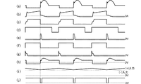
図10はスイッチング電源モジュール301の回路図、図11はその各部の波形図である。
このスイッチング電源モジュール301には、第2の実施形態で示した構造の複合トランスモジュール24によって、図10に示す第1の信号伝送トランス部15L、第2の信号伝送トランス部15R、電力伝送トランス部14を構成している。第1の信号伝送トランス部15Lは1次コイル15Lpと2次コイル15Lsを含み、第2の信号伝送トランス部15Rは1次コイル15Rpと2次コイル15Rsを含み、電力伝送トランス部14は1次コイル14p、2次コイル14s、および補助コイル14tを含んでいる。
FIG. 10 is a circuit diagram of the switching
The switching
ここで、直流入力電源の+入力端子115、直流入力電源の−入力端子116、平滑コンデンサ117,122、電力スイッチ118、同期整流器119,120、チョークコイル121、絶縁型スイッチング電源の+出力端子123、絶縁型スイッチング電源の−出力端子124によって電力変換回路を構成している。
Here, the +
また、マルチバイブレータ125、抵抗126,128,135,142,146,148,149、ダイオード127,133,134,139,144、インバータ129,130、コンデンサ131,138,143,145、ANDゲート132、MOS−FET136,137、NORゲート140、コンパレータ141、基準電圧源147によって制御回路を構成している。
Also, the
この絶縁型スイッチング電源は、一石共振リセットフォワードコンバータである。+入力端子115,−入力端子116の間に加わる直流入力電圧を、平滑コンデンサ117で平滑した後、電力伝送トランス部14の1次コイル14pを介して接続した電力スイッチ118でスイッチングさせて交流に変換する。
This insulated switching power supply is a one-stone resonant reset forward converter. The DC input voltage applied between the +
図10では表れていないが、多層基板の中脚部の周囲を巻回する位置に、信号処理回路に対する電源用のコイルパターンが形成されていて、この電源用のコイルパターンに誘起される電圧を整流平滑して信号処理回路へ電源電圧を供給する整流平滑回路を備えている。 Although not shown in FIG. 10, a coil pattern for power supply for the signal processing circuit is formed at a position wound around the middle leg portion of the multilayer substrate, and a voltage induced in the coil pattern for power supply is A rectifying / smoothing circuit that rectifies and smoothes and supplies a power supply voltage to the signal processing circuit is provided.
転流用の同期整流器120を制御するための構成(補助コイル14t、MOS−FET137、第1の信号伝送トランス部15L,ダイオード133)は特開2000−262051に開示されているように公知である。これは転流用の同期整流器120をオフさせるためのMOS−FET137を制御する信号の伝送にパルストランスを1つ用いるものであり、ここでは第1の信号伝送トランス部15Lをパルストランスとして用いている。
A configuration for controlling the
なお、電力伝送トランス部14は、1次コイル14p、2次コイル14s以外に補助コイル14tを備えているが、この補助コイル14tは、図7に示したコイル101a,103a以外に、これらと同様にして別のコイル配線を設けたものである。
The power
ところで、1次側のスイッチング素子である電力スイッチ118のオン・オフ制御は1次側に設けた制御回路で行う。この際の出力電圧の検出および制御方法には、トランスに設けた補助巻線の電圧を利用する間接制御型や2次側に出力電圧検出回路を設けてフォトカプラを介して1次側にフィードバックする直接制御型がある。間接制御型は出力電圧の検出精度が良くないという問題がある。直接制御型はフォトカプラを使うので使用温度条件が限られるという問題がある。さらに両者ともに、出力電圧の変動に対する応答性が悪いという問題がある。
By the way, on / off control of the
一方、応答性の良いスイッチング電源装置としてヒステリシス制御のスイッチング電源装置がある。
ヒステリシス制御は出力電圧と基準電圧をコンパレータで比較するので2次側に制御回路を備える必要があるが、2次側に電圧の発生していない起動時にその制御回路を動作させる電源が別途必要になるという問題がある。
On the other hand, there is a hysteresis-controlled switching power supply as a switching power supply with good response.
Hysteresis control uses a comparator to compare the output voltage and the reference voltage, so it is necessary to provide a control circuit on the secondary side, but a separate power supply is required to operate the control circuit at startup when no voltage is generated on the secondary side. There is a problem of becoming.
上記各問題の解決策として、起動時におけるソフトスタート時には1次側がスイッチング素子のオンオフタイミングを規定しつつ徐々にパルス幅を広げ、出力電圧が目標値に到達するとスイッチング素子のオフタイミングの信号を、2次側からパルストランスを介して1次側に伝達してスイッチング素子をオフさせ、スイッチング素子のオンタイミングは1次側制御回路が固定周期で規定するという制御方法(オンタイミングの信号を2次側から1次側に伝送し、オフタイミングを1次側制御回路が規定しても良い。)を本出願人は国際公開WO2007/018227にて出願している。これはヒステリシス制御を絶縁型に適用したコンバータであるために応答性が良く、しかも起動時は2次側からの信号がなくても動作するので2次側に制御回路の起動時用の電源が不要になる。 As a solution to each of the above problems, at the time of soft start at start-up, the primary side gradually defines the on / off timing of the switching element while gradually widening the pulse width, and when the output voltage reaches the target value, the switching element off timing signal is A control method in which the switching element is turned off by transmitting from the secondary side to the primary side via a pulse transformer, and the on-timing of the switching element is defined by the primary-side control circuit in a fixed cycle (the signal of the on-timing is secondary The primary side control circuit may define the off timing from the primary side to the primary side), and the present applicant has filed an application in International Publication WO2007 / 018227. Since this is a converter that applies hysteresis control to an insulation type, it has good responsiveness, and it operates even when there is no signal from the secondary side at startup, so there is a power supply for startup of the control circuit on the secondary side. It becomes unnecessary.
図10に示す例では、2次側から出力電圧と基準電圧との比較に基づいた電力スイッチ118のオフタイミング信号を第2の信号伝送トランス部15Rを介して1次側に伝達するように構成している。
In the example shown in FIG. 10, the off-timing signal of the
図11において、(a)は電力スイッチ118のドレイン電圧、(b)は電力スイッチ118のドレイン電流、(c)は電力スイッチ118のゲート電圧、(d)はマルチバイブレータ125の出力電圧、(e)は第2信号伝送トランス部15Rの1次コイル15Rpの電圧、(f)はANDゲート132の出力電圧、(g)は第1信号伝送トランス部15Lの2次コイル15Lsの電圧、(h)は同期整流器120のゲート電圧、(i)はコンパレータ141の一方の入力電圧、(j)はコンパレータ141の他方の入力電圧である。
11, (a) is the drain voltage of the
以下、この図11も参照して回路動作について説明する。
電力スイッチ118のオン期間に、前記交流を電力伝送トランス部14が、その1次コイル14pから2次コイル14sへ伝送し、整流側同期整流器119、転流側同期整流器120で整流した後、チョークコイル121、平滑コンデンサ122で構成する出力フィルタで平滑することで、交流を直流に変換して、+出力123,−出力124から直流電圧を出力する。
The circuit operation will be described below with reference to FIG.
While the
電力スイッチ118のオフ後、電力伝送トランス部14の励磁インダクタンスと電力スイッチ118の等価的な並列寄生容量とがLC共振してトランスがリセットされる(図11(a)(b)参照)。
After the
トランスのリセット完了後の電力スイッチ118のオフ期間においては、トランス励磁電流が電力伝送トランス部14の2次コイル14s→同期整流器120→同期整流器119の寄生ダイオードのループで還流するので、電力伝送トランス部14の両端電圧がゼロボルトにクランプされ、電力スイッチ118のドレイン電圧は入力電圧にクランプされる。
上記のサイクルを繰り返して電力変換を行う。
In the off period of the
The above cycle is repeated to perform power conversion.
上記制御回路内のマルチバイブレータ125は固定周波数で発振動作する(図11(d)参照)。マルチバイブレータ125のオンタイミングにはMOS−FET136のドレイン電圧もハイレベルであることから、マルチバイブレータ125のオンと同時にANDゲート132の出力もハイレベルとなる(図11(f)参照)。
The
ANDゲート132がオンすると、第1の信号伝送トランス部15Lの1次コイル15Lpを通して電力スイッチ118のゲートが充電される(図11(c)参照)。このとき発生するパルス信号が第1の信号伝送トランス部15Lの1次コイル15Lpから2次コイル15Lsに伝送されMOS−FET137がオンする(図11(g)参照)。MOS−FET137がオンすると、転流側同期整流器120のゲート蓄積電荷が放電されてオフする(図11(h)参照)。
When the AND
電力スイッチ118は、そのゲート充電経路に第1の信号伝送トランス部15Lの1次コイル15Lpがあることで、一定時間の遅れをともなってオンする。この動作により、電力スイッチ118のオン直前に転流側同期整流器120がオフするので、転流側同期整流器120のターンオフ遅れを原因とする短絡電流が発生せず、高効率の電力変換動作が可能になる。
The
上記制御回路は、入力電圧、出力電流の過渡変化に対して高速応答させるために、PID制御ではなく、コンパレータによるヒステリシス制御を行う。 The control circuit performs hysteresis control by a comparator instead of PID control in order to make high-speed response to transient changes in input voltage and output current.
コンパレータ141の反転入力には出力電圧を抵抗148,149で分圧した電圧を入力し、その非反転入力には、基準電圧源147の電圧を抵抗146を介して入力している。コンパレータ141はこの両者を比較する。
A voltage obtained by dividing the output voltage by
出力電圧にはリップル電圧が重畳されていて、コンパレータ141の非反転入力に入力する電圧には抵抗142,146、コンデンサ145によって、上記リップル電圧とは逆の傾きのランプ電圧が重畳されている(図11(i)参照)。
A ripple voltage is superimposed on the output voltage, and a ramp voltage having a slope opposite to that of the ripple voltage is superimposed on the voltage input to the non-inverting input of the
電力スイッチ118のオン期間の途中でコンパレータ141の反転入力電圧が非反転入力電圧を上回ると、コンパレータ141の出力電圧がローレベルになり、NORゲート140に入力される(図11(j)参照)。
When the inverting input voltage of the
NORゲート140のもう一方の入力は電力スイッチ118のオン期間にローレベルになるので、NORゲート140の出力はローレベルからハイレベルになり、コンデンサ138を介して第2の信号伝送トランス部15Rの1次コイル15Rpに電流が流れてパルス信号が発生する。このパルス信号は第2の信号伝送トランス部15Rの1次コイル15Rpから2次コイル15Rsに伝送され、MOS−FET136がオンする(図11(e)参照)。
Since the other input of the NOR
MOS−FET136のドレインには、インバータ129のオン期間(マルチバイブレータ125のオフ期間)にダイオード134、抵抗135を通して電荷が蓄積されているが、MOS−FET136のオンによって、MOS−FET136のドレインはハイレベルからローレベルになる。MOS−FET136のドレインがローレベルになると、ANDゲート132の出力もローレベルになり、ダイオード133を介して電力スイッチ118のゲート蓄積電荷が放電されて電力スイッチ118がオフする。
In the drain of the MOS-
このようにして、電力スイッチ118をオフさせるパルス信号のタイミングを制御することで、電力スイッチ118のオン期間を制御する。電力スイッチ118のオフ期間の長さは、マルチバイブレータ125の発振周期から電力スイッチ118のオン期間を引いた値になるので、実質的に2次側の回路が主導してPWM制御が行われ、出力電圧が安定化される。この制御方法はPID制御のように誤差アンプやフォトカプラに起因する位相遅れがなく、入力電圧、出力電流の過渡変動に起因する出力電圧変動に対して、変動が発生した周期に直ちに応答するパルスバイパルス動作が可能となる。
In this way, the ON period of the
このように、複合トランスモジュール24を、導体パターンで形成された積層型トランスで構成することで、スイッチング電源を薄型化できる。高速応答制御回路、同期整流器駆動回路、保護回路の設計やトランスの設計を省くことができ、スイッチング電源の設計に要する工数とコストを削減することができる点は第1の実施形態と同じである。
Thus, the switching power supply can be thinned by configuring the
複合トランスモジュール24を高放熱性基板27に実装したスイッチング電源モジュール301において、特に発熱の大きな電力変換回路の回路構成部品の放熱性を重視する場合は、高放熱性基板27としてアルミ基板などの高放熱性基板を用い、その高放熱性基板27に前記電力変換回路部品を実装し、高放熱性基板27をヒートシンクに密着させる。この構造によれば高い放熱性が得られる。
In the switching
なお、スイッチング電源の出力電圧ではなく、出力電流との相関性のある信号を2次側から1次側に送信する機能を備え、1次信号処理回路が出力電流との相関性のある信号を受信し、出力電流が目標値に漸近するように1次電力スイッチの駆動信号幅を制御するパルス幅制御機能を備えてもよい。 In addition, it has a function of transmitting a signal having a correlation with the output current instead of the output voltage of the switching power supply from the secondary side to the primary side, and the primary signal processing circuit outputs a signal having a correlation with the output current. A pulse width control function for receiving and controlling the drive signal width of the primary power switch so that the output current gradually approaches the target value may be provided.
また、電力伝送トランス部14の1次コイル又は2次コイルの過電流状態、電力伝送トランス部14の過熱状態、スイッチング電源の入力電圧の低電圧状態・過電圧状態、スイッチング電源の出力電圧の低電圧状態・過電圧状態の少なくとも何れかの異常状態を検出する検出回路を備え、異常動作を検出すると、1次電力スイッチのデューティの低減、スイッチング動作の停止、又はヒカップ動作、の何れかを行うことでスイッチング電源を保護する異常動作保護手段を備えてもよい。
Moreover, the overcurrent state of the primary coil or the secondary coil of the power
《第3の実施形態》
図12は第3の実施形態に係るスイッチング電源モジュール302の回路図である。
このスイッチング電源モジュール302には、第2の実施形態で示した構造の複合トランスモジュール24と基本的に同様の構成によって、図12に示す第1の信号伝送トランス部209、第2の信号伝送トランス部210、電力伝送トランス部208を構成している。第1の信号伝送トランス部209は1次コイル209Aと2次コイル209Bを含み、第2の信号伝送トランス部210は1次コイル210Aと2次コイル210Bを含み、電力伝送トランス部208は1次コイル208A、2次コイル208B、および補助コイル208Cを含んでいる。
<< Third Embodiment >>
FIG. 12 is a circuit diagram of the switching
The switching
このスイッチング電源モジュール302は、いわゆるダブルエンド絶縁型DC−DCコンバータ(ハーフブリッジコンバータ)を構成している。1次コイル208Aおよび2次コイル208Bを有する電力伝送トランス部208、この電力伝送トランス208の1次側に接続される第1の電力スイッチ204および第2の電力スイッチ(ハイサイド電力スイッチ)205、第1・第2の電力スイッチ204,205をスイッチング制御する1次側制御回路280と、電力伝送トランス部208の2次側に接続される第1の同期整流器211、第2の同期整流器212、チョークコイル213を備えている。
This switching
また、1次側制御回路280からの信号に基づいて第1の電力スイッチ204のターンオンおよびターンオフのタイミングにほぼ対応する第1のターンオフエッジ信号および第1のターンオンエッジ信号を発生する第1のエッジ信号発生回路271と、1次側制御回路270からの信号に基づいて第2の電力スイッチ205のターンオンおよびターンオフのタイミングにほぼ対応する第2のターンオフエッジ信号および第2のターンオンエッジ信号を発生する第2のエッジ信号発生回路272を備えている。
Also, a first edge that generates a first turn-off edge signal and a first turn-on edge signal that substantially correspond to the turn-on and turn-off timings of the
また、第1のターンオフエッジ信号および第1のターンオンエッジ信号を2次側へ伝送する第1の信号伝送トランス部209と、第2のターンオフエッジ信号および第2のターンオンエッジ信号を2次側へ伝送する第2の信号伝送トランス部210と、第1の信号伝送トランス部209によって伝送された第1のターンオフエッジ信号で第1の同期整流器211をターンオフし、第1の信号伝送トランス部209によって伝送された第1のターンオンエッジ信号で第1の同期整流器211をターンオンする第1の同期整流器制御回路273を備えている。さらに、第2の信号伝送トランス部210によって伝送された第2のターンオフエッジ信号で第2の同期整流器212をターンオフし、第2の信号伝送トランス部210によって伝送された第2のターンオンエッジ信号で第2の同期整流器212をターンオンする第2の同期整流器制御回路274を備えている。
Also, a first
入力直流電源201のライン間には第1・第2の電力スイッチ204,205およびコンデンサ206,207の直列回路をそれぞれ接続していて、第1・第2の電力スイッチ204,205の接続点とコンデンサ206,207の接続点との間に電力伝送トランス部208の1次コイル208Aを接続している。
A series circuit of first and second power switches 204 and 205 and
電力伝送トランス部208の2次コイル208B、208Cの接続点にはチョークコイル213の一端を接続し、チョークコイル213の他端と2次側グランドとに間に出力平滑コンデンサ214を接続している。
One end of the
電力伝送トランス部208の2次コイル208Bの一端と2次側グランドとの間には第1の同期整流器211を接続している。また、電力伝送トランス部208の2次コイル208Cの一端と2次側グランドとの間には第2の同期整流器212を接続している。
A first
このスイッチング電源モジュール302の入力には入力直流電源201が接続され、出力には負荷215が接続される。また、1次側制御回路電源入力部216には制御電源電圧が印加される。
An input
第1のエッジ信号発生回路271は、ショットキーバリアダイオード(以下、「SBD」)219,220、およびコンデンサ222で構成していて、1次側制御回路電源入力部216と1次側のグランドとの間に接続している。同様に、第2のエッジ信号発生回路272は、SBD217,218、およびコンデンサ221で構成していて、1次側制御回路電源入力部216と1次側のグランドとの間に接続している。
The first edge
PWM制御回路202の第1のPWM信号出力端子2Aと第1のエッジ信号発生回路271との間には第1の信号伝送トランス部209の1次コイル209Aを接続している。同様に、PWM制御回路202の第2のPWM信号出力端子2Bと第2のエッジ信号発生回路272との間には第2の信号伝送トランス部210の1次コイル210Aを接続している。
A
第1の同期整流器制御回路273は、NチャネルMOSFET224、PチャネルMOSFET225、ダイオード(PNダイオード)226,227、ツェナーダイオード229、抵抗228を備えている。同様に、第2の同期整流器制御回路274は、NチャネルMOSFET235、PチャネルMOSFET236、ダイオード(PNダイオード)232,233、ツェナーダイオード230、抵抗231を備えている。
The first synchronous
FET224、FET225、抵抗223の直列回路は2次側制御回路電源入力部237と2次側グランドとの間に接続し、FET224とFET225の接続点はNチャネルMOSFETである第1の同期整流器211のゲートに接続している。同様にFET235、FET236、抵抗234の直列回路は2次側制御回路電源入力部237と2次側グランドとの間に接続し、FET235とFET236の接続点はNチャネルMOSFETである第2の同期整流器212のゲートに接続している。
The series circuit of the
また、第1の同期整流器制御回路273のダイオード226,227の接続点とFET224,225の接続点との間に第1の信号伝送トランス部209の2次コイル209Bを接続している。同様に、第2の同期整流器制御回路274のダイオード232,233の接続点とFET235,236の接続点との間に第2の信号伝送トランス部210の2次コイル210Bを接続している。
Further, the
前記1次側制御回路280は、ハイサイドドライバICを用いることなく、基準電位(ソース)がグランドと非接続の第2の電力スイッチ205を第2の信号伝送トランス部210を用いて駆動するように構成している。
The primary
第2の電力スイッチ205の駆動用電力を確保するために、コンデンサ256及びダイオード255からなるブートストラップ回路254を設けている。このブートストラップ回路254の出力部と1次側グランドとの間に、FET258、FET259、抵抗257の直列回路を接続し、FET258とFET259の接続点は第2の電力スイッチ205のゲートに接続している。FET258とFET259のゲートにはダイオード260,261、ツェナーダイオード263、抵抗262からなる回路を接続している。そして、ダイオード260,261の接続点とFET258,259の接続点との間に第2の信号伝送トランス部210の3次コイル210Cを接続している。
In order to secure driving power for the
また、抵抗264とSBD265による第1の電力スイッチ側遅延回路278をPWM制御回路202の第1のPWM信号出力端子202Aと第1の電力スイッチ204のゲートとの間に設けている。
A first power switch
図12において、電力スイッチ204,205、コンデンサ206,207、同期整流器211,212、チョークコイル213、出力平滑コンデンサ214、入力直流電源201、及び負荷215以外が複合トランスモジュールで構成されている。
In FIG. 12, components other than the power switches 204 and 205,
このスイッチング電源モジュール302の動作は次のとおりである。先ず、第2の信号伝送トランス部210の3次コイルから出力される第2のターンオフエッジ信号はダイオード260を通してFET258のゲートに印加され、FET258がターンオンし、第2の電力スイッチ205のゲートに電荷が充電されて第2の電力スイッチ205がターンオンされる。その後、第2のターンオンエッジ信号は、ダイオード261を通してFET259のゲートに印加されてFET259がターンオンし、第2の電力スイッチ205のゲートの電荷が放電され、第2の電力スイッチ205がターンオフされる。
The operation of this switching
第2の信号伝送トランス部210の極性に応じて、電力スイッチ205はPWM制御回路202が出力した第2のPWM信号と同じタイミングで駆動され、第2の同期整流器212は反転したタイミングで駆動されるため、第2の電力スイッチ205と第2の同期整流器212とはほぼ相補的なタイミングで駆動される。同様にして、第1の電力スイッチ204と第1の同期整流器211がほぼ相補的なタイミングで駆動される。なお、第2の電力スイッチ205のゲートの充電電流は抵抗257で制限される。このことにより、第2の遅延時間が確保される。また、第1の電力スイッチ側遅延回路278で電力スイッチ204のゲート充電電流が制限される。このことによって第1の遅延時間が確保される。
In accordance with the polarity of the second
《他の実施形態》
この発明は以上に示した実施形態に限らず様々な実施形態を採り得る。例えば、複合トランスのコア形状は様々な応用形態があり、コア18の中脚、外脚の断面は、円形や楕円形などの他の形状でもよい。また、特開平11−340058のように同心円状に複数のトランスを構成してもよい。
<< Other embodiments >>
This invention can take not only the embodiment shown above but various embodiments. For example, the core shape of the composite transformer has various applications, and the cross section of the middle leg and the outer leg of the core 18 may be other shapes such as a circle and an ellipse. A plurality of transformers may be configured concentrically as disclosed in JP-A-11-340058.
なお、この発明は以上に示した実施形態に限らず様々な実施形態を採り得る。例えば、各実施形態では中脚、外脚の断面を共に長方形や円形以外に楕円形など他の形状でもよい。 In addition, this invention can take not only the embodiment shown above but various embodiment. For example, in each embodiment, the cross section of the middle leg and the outer leg may be other shapes such as an ellipse in addition to a rectangle or a circle.
また、コアは5本脚のコアに限らず、4本脚のコアを用いて一つの電力伝送トランス部一つの信号伝送トランス部を設けてもよい。
また、コアの中脚の接合部に磁気ギャップを設けて、電力伝送トランス部の直流重畳特性を改善してもよい。
The core is not limited to a five-leg core, and a single leg transmission transformer section may be provided using a four-leg core.
In addition, a magnetic gap may be provided at the joint portion of the middle leg of the core to improve the DC superposition characteristics of the power transmission transformer unit.
また、コア18を嵌め合わせる方法は、コア留め用の金具を用いてもよいし、プラスチック等、他の材質でコア留め用の部品を形成してもよい。コア留め用の部品を使用せず、接着剤によってコア同士を接着してもよい。 Moreover, the method of fitting the cores 18 may use metal fittings for core fastening, or may form parts for core fastening with other materials such as plastic. You may adhere | attach cores by an adhesive agent, without using the component for core fastening.
また、電力伝送トランス部を形成するコイルは、プリント基板に導体パターンを形成してもよいし、線材をボビンに巻いて形成しても良く、ボビンに銅箔を絶縁シートを介して巻回しても良く、それ以外の公知のコイル形成方法も問題なく適用できる。 In addition, the coil forming the power transmission transformer part may be formed by forming a conductor pattern on a printed circuit board, or by winding a wire rod around a bobbin, and winding a copper foil around the bobbin via an insulating sheet. Other well-known coil forming methods can be applied without any problem.
また、この発明のスイッチング電源モジュールにおいて、信号伝送トランス15は、同期整流器の駆動や、出力電圧、出力電流の制御、あるいは電力伝送コイル部の過電流状態、過熱状態、スイッチング電源の入力電圧の低電圧状態、過電圧状態、スイッチング電源の出力電圧の低電圧状態、又は過電圧状態などの異常動作を検出してスイッチング電源を保護する各種保護回路での利用以外に、他の用途にも応用可能である。また、例えばデジタル信号の伝送に用いてもよい。 Further, in the switching power supply module of the present invention, the signal transmission transformer 15 is configured to drive the synchronous rectifier, control the output voltage and output current, or reduce the overcurrent state, overheat state, and input voltage of the switching power source. In addition to the use in various protection circuits that protect the switching power supply by detecting abnormal operation such as voltage state, overvoltage state, undervoltage state of switching power supply output voltage, or overvoltage state, it can be applied to other uses . For example, it may be used for transmission of a digital signal.
12…複合トランスモジュール
13…多層基板
14…電力伝送トランス部
14t…補助コイル
14p…1次コイル
15L,15R…信号伝送トランス部
14s…2次コイル
15Lp…1次コイル
15Rp…1次コイル
16…複合トランス
15Ls…2次コイル
15Rs…2次コイル
17…1次信号処理回路
18BLa,18BLb,18BRa,18BRb…外脚
18T,18B…コア
18TC,18BC…中脚
19C,19La,19Lb,19Ra,19Rb…コア脚挿通孔
20…ボビン
21…接続端子挿通孔
23…接続端子
22…2次信号処理回路
24…複合トランスモジュール
25…放熱シート
26…接続端子
27…高放熱性基板
28…スイッチ素子
29…入出力フィルタ
31…接続端子
101a,103a…コイル
102a,102c…コイル
102b…ビア電極
103a…コイル
104a,104c…コイル
104b…ビア電極
115…入力端子
117,122…平滑コンデンサ
118…電力スイッチ
119…整流側同期整流器
120…転流側同期整流器
121…チョークコイル
105a,105c…コイル
105b…ビア電極
123…出力端子
106a,106c…コイル
106b…ビア電極
124…出力端子
125…マルチバイブレータ
129,130…インバータ
132…ANDゲート
136,137…MOS−FET
301,302…スイッチング電源モジュール
DESCRIPTION OF
301, 302 ... switching power supply module
Claims (12)
前記信号伝送トランス部は、前記コアの磁脚を貫通させた多層基板及び当該多層基板に形成されたコイルパターンで構成され、
信号伝送トランス部の入出力信号を処理する信号処理回路が前記多層基板に実装され、
前記複合トランスと前記信号処理回路とがモジュールとして一体形成されたことを特徴とする複合トランスモジュール。 One set of cores, a power transmission transformer unit for transmitting power between the primary and secondary, and a signal transmission transformer for transmitting a signal between the primary and secondary substantially independently of the power transmission transformer unit A composite transformer having
The signal transmission transformer unit is composed of a multilayer substrate that penetrates the magnetic legs of the core and a coil pattern formed on the multilayer substrate,
A signal processing circuit for processing input / output signals of the signal transmission transformer is mounted on the multilayer substrate,
A composite transformer module, wherein the composite transformer and the signal processing circuit are integrally formed as a module.
前記電源用のコイルパターンに誘起される電圧を整流平滑して前記信号処理回路へ電源電圧を供給する整流平滑回路を備えた、請求項5又6に記載の複合トランスモジュール。 A coil pattern for a power source for the signal processing circuit is formed at a position wound around the middle leg portion of the multilayer substrate,
7. The composite transformer module according to claim 5, further comprising a rectifying / smoothing circuit that rectifies and smoothes a voltage induced in the coil pattern for power supply and supplies a power supply voltage to the signal processing circuit.
前記1次信号処理回路は、前記出力電圧又は出力電流との相関性のある信号を受信し、前記出力電圧又は出力電流が目標値に漸近するように1次電力スイッチの駆動信号幅を制御するパルス幅制御機能と、前記1次電力スイッチの駆動信号を出力する手段とを備えた、請求項8に記載の複合トランスモジュール。 The secondary signal processing circuit has a function of transmitting a signal having a correlation with an output voltage or an output current of the isolated switching power supply from the secondary side to the primary side,
The primary signal processing circuit receives a signal having a correlation with the output voltage or output current, and controls the drive signal width of the primary power switch so that the output voltage or output current approaches a target value. 9. The composite transformer module according to claim 8, comprising a pulse width control function and means for outputting a drive signal for the primary power switch.
前記1次信号処理回路は、前記1次電力スイッチの駆動タイミングと関連した前記ハイサイド電力スイッチの駆動信号をモジュールから出力する手段を備えた、請求項9に記載の複合トランスモジュール。 The isolated switching power supply includes a high-side power switch having a drive signal reference potential different from that of the primary power switch on the primary side,
The composite transformer module according to claim 9, wherein the primary signal processing circuit includes means for outputting a drive signal of the high-side power switch related to the drive timing of the primary power switch from the module.
前記2次信号処理回路は、前記同期整流器の駆動タイミングと関連する信号を受信して、同期整流器の駆動信号を形成してモジュールから出力する回路を備える、請求項8乃至10の何れかに記載の複合トランスモジュール。 The primary signal processing circuit includes a circuit for transmitting a signal related to the driving timing of the synchronous rectifier from the primary side to the secondary side,
The said secondary signal processing circuit is provided with the circuit which receives the signal relevant to the drive timing of the said synchronous rectifier, forms the drive signal of a synchronous rectifier, and outputs it from a module. Composite transformer module.
前記検出回路が異常動作を検出すると、前記1次電力スイッチのデューティの低減、スイッチング動作の停止、又はヒカップ動作、の何れかを行うことで前記絶縁型スイッチング電源を保護する異常動作保護手段を備えた、請求項8乃至11の何れかに記載の複合トランスモジュール。 The signal processing circuit includes: an overcurrent state of a primary coil or a secondary coil of the power transmission transformer unit; an overheat state of the power transmission transformer unit; a low voltage state of an input voltage of the insulated switching power supply; A detection circuit for detecting an abnormal state of at least one of an overvoltage state of the input voltage, an undervoltage state of the output voltage of the isolated switching power supply, and an overvoltage state of the output voltage of the isolated switching power supply;
When the detection circuit detects an abnormal operation, the abnormal power protection means protects the isolated switching power supply by performing any one of a duty reduction of the primary power switch, a switching operation stop, or a hiccup operation. The composite transformer module according to any one of claims 8 to 11.
Priority Applications (1)
| Application Number | Priority Date | Filing Date | Title |
|---|---|---|---|
| JP2010055996A JP2011192724A (en) | 2010-03-12 | 2010-03-12 | Composite transformer module |
Applications Claiming Priority (1)
| Application Number | Priority Date | Filing Date | Title |
|---|---|---|---|
| JP2010055996A JP2011192724A (en) | 2010-03-12 | 2010-03-12 | Composite transformer module |
Publications (1)
| Publication Number | Publication Date |
|---|---|
| JP2011192724A true JP2011192724A (en) | 2011-09-29 |
Family
ID=44797356
Family Applications (1)
| Application Number | Title | Priority Date | Filing Date |
|---|---|---|---|
| JP2010055996A Pending JP2011192724A (en) | 2010-03-12 | 2010-03-12 | Composite transformer module |
Country Status (1)
| Country | Link |
|---|---|
| JP (1) | JP2011192724A (en) |
Cited By (6)
| Publication number | Priority date | Publication date | Assignee | Title |
|---|---|---|---|---|
| WO2015136957A1 (en) * | 2014-03-12 | 2015-09-17 | 日立オートモティブシステムズ株式会社 | Transformer and power conversion apparatus using same |
| KR101590132B1 (en) * | 2015-07-31 | 2016-02-01 | 삼성전기주식회사 | Transformer and plate coil shaped parts |
| KR200487142Y1 (en) * | 2017-05-31 | 2018-08-10 | 주식회사 에이치에스씨 | A transformer-purpose guider having a secondary coil formed integrally therewith |
| JPWO2019138861A1 (en) * | 2018-01-09 | 2020-04-16 | 三菱電機株式会社 | Coil device and power converter |
| CN111313721A (en) * | 2020-03-31 | 2020-06-19 | 佛山力昊电源技术有限公司 | Novel synchronous rectification power supply capable of being connected in parallel |
| CN113643885A (en) * | 2021-08-16 | 2021-11-12 | 上海激光电源设备有限责任公司 | Primary coil structure and high-voltage pulse transformer thereof |
Citations (11)
| Publication number | Priority date | Publication date | Assignee | Title |
|---|---|---|---|---|
| JPS61176991U (en) * | 1985-04-23 | 1986-11-05 | ||
| JPH0718424U (en) * | 1993-08-31 | 1995-03-31 | 株式会社日本プロテクター | Hybrid circuit with transformer |
| JPH07163146A (en) * | 1993-12-07 | 1995-06-23 | Murata Mfg Co Ltd | Dc-dc converter |
| JPH08241816A (en) * | 1995-03-03 | 1996-09-17 | West Electric Co Ltd | Trigger transformer |
| JP2000228318A (en) * | 1999-02-04 | 2000-08-15 | Matsushita Electric Ind Co Ltd | Converter transformer |
| JP2001230133A (en) * | 2000-02-16 | 2001-08-24 | Sanshin Denki Kk | Transformer unit for resonance switching power supply |
| JP2003197439A (en) * | 2001-12-28 | 2003-07-11 | Ikeda Electric Co Ltd | Electromagnetic device |
| JP2005110452A (en) * | 2003-10-01 | 2005-04-21 | Murata Mfg Co Ltd | Switching power supply module |
| WO2007069403A1 (en) * | 2005-12-16 | 2007-06-21 | Murata Manufacturing Co., Ltd. | Composite transformer and insulated switching power supply |
| WO2008041399A1 (en) * | 2006-10-02 | 2008-04-10 | Murata Manufacturing Co., Ltd. | Double ended insulation dc-dc converter |
| JP2008205350A (en) * | 2007-02-22 | 2008-09-04 | Oki Power Tech Co Ltd | Magnetic device |
-
2010
- 2010-03-12 JP JP2010055996A patent/JP2011192724A/en active Pending
Patent Citations (11)
| Publication number | Priority date | Publication date | Assignee | Title |
|---|---|---|---|---|
| JPS61176991U (en) * | 1985-04-23 | 1986-11-05 | ||
| JPH0718424U (en) * | 1993-08-31 | 1995-03-31 | 株式会社日本プロテクター | Hybrid circuit with transformer |
| JPH07163146A (en) * | 1993-12-07 | 1995-06-23 | Murata Mfg Co Ltd | Dc-dc converter |
| JPH08241816A (en) * | 1995-03-03 | 1996-09-17 | West Electric Co Ltd | Trigger transformer |
| JP2000228318A (en) * | 1999-02-04 | 2000-08-15 | Matsushita Electric Ind Co Ltd | Converter transformer |
| JP2001230133A (en) * | 2000-02-16 | 2001-08-24 | Sanshin Denki Kk | Transformer unit for resonance switching power supply |
| JP2003197439A (en) * | 2001-12-28 | 2003-07-11 | Ikeda Electric Co Ltd | Electromagnetic device |
| JP2005110452A (en) * | 2003-10-01 | 2005-04-21 | Murata Mfg Co Ltd | Switching power supply module |
| WO2007069403A1 (en) * | 2005-12-16 | 2007-06-21 | Murata Manufacturing Co., Ltd. | Composite transformer and insulated switching power supply |
| WO2008041399A1 (en) * | 2006-10-02 | 2008-04-10 | Murata Manufacturing Co., Ltd. | Double ended insulation dc-dc converter |
| JP2008205350A (en) * | 2007-02-22 | 2008-09-04 | Oki Power Tech Co Ltd | Magnetic device |
Cited By (11)
| Publication number | Priority date | Publication date | Assignee | Title |
|---|---|---|---|---|
| WO2015136957A1 (en) * | 2014-03-12 | 2015-09-17 | 日立オートモティブシステムズ株式会社 | Transformer and power conversion apparatus using same |
| JP2015173188A (en) * | 2014-03-12 | 2015-10-01 | 日立オートモティブシステムズ株式会社 | Transformer and power converter using the same |
| CN106104723A (en) * | 2014-03-12 | 2016-11-09 | 日立汽车系统株式会社 | Transformer and the power inverter using this transformer |
| US10381148B2 (en) | 2014-03-12 | 2019-08-13 | Hitachi Automotive Systems, Ltd. | Transformer and power converter using the same |
| KR101590132B1 (en) * | 2015-07-31 | 2016-02-01 | 삼성전기주식회사 | Transformer and plate coil shaped parts |
| US10388449B2 (en) | 2015-07-31 | 2019-08-20 | Solum Co., Ltd. | Transformer and plate coil molded body |
| KR200487142Y1 (en) * | 2017-05-31 | 2018-08-10 | 주식회사 에이치에스씨 | A transformer-purpose guider having a secondary coil formed integrally therewith |
| JPWO2019138861A1 (en) * | 2018-01-09 | 2020-04-16 | 三菱電機株式会社 | Coil device and power converter |
| CN111313721A (en) * | 2020-03-31 | 2020-06-19 | 佛山力昊电源技术有限公司 | Novel synchronous rectification power supply capable of being connected in parallel |
| CN113643885A (en) * | 2021-08-16 | 2021-11-12 | 上海激光电源设备有限责任公司 | Primary coil structure and high-voltage pulse transformer thereof |
| CN113643885B (en) * | 2021-08-16 | 2024-05-14 | 上海激光电源设备有限责任公司 | Primary coil structure and high-voltage pulse transformer thereof |
Similar Documents
| Publication | Publication Date | Title |
|---|---|---|
| JP4803262B2 (en) | Isolated switching power supply | |
| US7872561B2 (en) | Composite transformer and insulated switching power source device | |
| EP1760867B1 (en) | Switching power supply unit | |
| Chen et al. | Design of high efficiency, low profile, low voltage converter with integrated magnetics | |
| Huang et al. | LLC resonant converter with matrix transformer | |
| US6714428B2 (en) | Combined transformer-inductor device for application to DC-to-DC converter with synchronous rectifier | |
| US7623362B2 (en) | Switching power supply unit | |
| US9124190B2 (en) | Isolated switched mode power supply | |
| US10381914B2 (en) | Integrated transformer | |
| US20110101951A1 (en) | Zero-Voltage-Switching Self-Driven Full-Bridge Voltage Regulator | |
| JP2004524788A (en) | Method and circuit for reducing reverse current in a synchronous rectifier converter circuit | |
| JP2004274262A (en) | Electrically insulated switch element driving circuit | |
| JP2011192724A (en) | Composite transformer module | |
| JP5939274B2 (en) | Power supply | |
| JP5338225B2 (en) | Switching power supply | |
| KR20190016479A (en) | DC / DC converter | |
| Park et al. | Design considerations of 1 MHz LLC resonant converter with GaN E-HEMT | |
| JP2004297994A (en) | Isolated switching dc/dc converter | |
| JP5795927B2 (en) | Switching power supply | |
| JP5776841B2 (en) | Switching power supply | |
| JP5522824B2 (en) | Switching element loss reduction circuit | |
| JP4013952B2 (en) | DC-DC converter | |
| Hoffmann et al. | Overcoming design challenges in low voltage GaN based PSFB battery charger | |
| JP3507827B2 (en) | Multi-output switching power supply circuit | |
| JP2003244935A (en) | Electrically insulating switching element drive circuit |
Legal Events
| Date | Code | Title | Description |
|---|---|---|---|
| A621 | Written request for application examination |
Free format text: JAPANESE INTERMEDIATE CODE: A621 Effective date: 20130108 |
|
| A977 | Report on retrieval |
Free format text: JAPANESE INTERMEDIATE CODE: A971007 Effective date: 20131015 |
|
| A131 | Notification of reasons for refusal |
Free format text: JAPANESE INTERMEDIATE CODE: A131 Effective date: 20131022 |
|
| A02 | Decision of refusal |
Free format text: JAPANESE INTERMEDIATE CODE: A02 Effective date: 20140304 |