JP2011100991A - Semiconductor device and method for manufacturing the same - Google Patents
Semiconductor device and method for manufacturing the same Download PDFInfo
- Publication number
- JP2011100991A JP2011100991A JP2010226200A JP2010226200A JP2011100991A JP 2011100991 A JP2011100991 A JP 2011100991A JP 2010226200 A JP2010226200 A JP 2010226200A JP 2010226200 A JP2010226200 A JP 2010226200A JP 2011100991 A JP2011100991 A JP 2011100991A
- Authority
- JP
- Japan
- Prior art keywords
- layer
- electrode layer
- oxide semiconductor
- thin film
- substrate
- Prior art date
- Legal status (The legal status is an assumption and is not a legal conclusion. Google has not performed a legal analysis and makes no representation as to the accuracy of the status listed.)
- Granted
Links
Images


Classifications
-
- H—ELECTRICITY
- H10—SEMICONDUCTOR DEVICES; ELECTRIC SOLID-STATE DEVICES NOT OTHERWISE PROVIDED FOR
- H10D—INORGANIC ELECTRIC SEMICONDUCTOR DEVICES
- H10D30/00—Field-effect transistors [FET]
- H10D30/60—Insulated-gate field-effect transistors [IGFET]
- H10D30/67—Thin-film transistors [TFT]
- H10D30/674—Thin-film transistors [TFT] characterised by the active materials
- H10D30/6755—Oxide semiconductors, e.g. zinc oxide, copper aluminium oxide or cadmium stannate
-
- H—ELECTRICITY
- H10—SEMICONDUCTOR DEVICES; ELECTRIC SOLID-STATE DEVICES NOT OTHERWISE PROVIDED FOR
- H10D—INORGANIC ELECTRIC SEMICONDUCTOR DEVICES
- H10D30/00—Field-effect transistors [FET]
- H10D30/01—Manufacture or treatment
- H10D30/021—Manufacture or treatment of FETs having insulated gates [IGFET]
- H10D30/031—Manufacture or treatment of FETs having insulated gates [IGFET] of thin-film transistors [TFT]
-
- H—ELECTRICITY
- H10—SEMICONDUCTOR DEVICES; ELECTRIC SOLID-STATE DEVICES NOT OTHERWISE PROVIDED FOR
- H10D—INORGANIC ELECTRIC SEMICONDUCTOR DEVICES
- H10D64/00—Electrodes of devices having potential barriers
- H10D64/60—Electrodes characterised by their materials
- H10D64/62—Electrodes ohmically coupled to a semiconductor
Landscapes
- Thin Film Transistor (AREA)
- Electrodes Of Semiconductors (AREA)
Abstract
【課題】酸化物半導体層を用いる薄膜トランジスタにおいて、酸化物半導体層に用いられる材料とソース電極層またはドレイン電極層に用いられる材料とが相互反応することを防ぐ構造を提供することを課題の一とする。
【解決手段】絶縁表面を有する基板上に設けるソース電極層またはドレイン電極層を2層以上の積層構造とし、その積層のうち、酸化物半導体層と接する一層を酸化物半導体層の構成金属元素以外の金属層とする。用いる金属層の材料としては、Sn、Sb、Se、Te、Pd、Ag、Ni、Cuから選ばれた元素、または上述した元素を成分とする合金か、上述した元素を組み合わせた合金等を用いる。
【選択図】図1An object of the present invention is to provide a structure in which a material used for an oxide semiconductor layer and a material used for a source electrode layer or a drain electrode layer are prevented from reacting with each other in a thin film transistor using an oxide semiconductor layer. To do.
A source electrode layer or a drain electrode layer provided over a substrate having an insulating surface has a stacked structure of two or more layers, and one layer in contact with the oxide semiconductor layer is not a constituent metal element of the oxide semiconductor layer. The metal layer. As a material for the metal layer to be used, an element selected from Sn, Sb, Se, Te, Pd, Ag, Ni, Cu, an alloy containing the above-described elements as a component, or an alloy combining the above-described elements is used. .
[Selection] Figure 1
Description
薄膜トランジスタ(以下、TFTという)で構成された回路を有する半導体装置およびその作製方法に関する。例えば、液晶表示パネルに代表される電気光学装置や有機発光素子を有する発光表示装置を部品として搭載した電子機器に関する。 The present invention relates to a semiconductor device having a circuit including a thin film transistor (hereinafter referred to as TFT) and a manufacturing method thereof. For example, the present invention relates to an electronic apparatus in which an electro-optical device typified by a liquid crystal display panel or a light-emitting display device having an organic light-emitting element is mounted as a component.
なお、本明細書中において半導体装置とは、半導体特性を利用することで機能しうる装置全般を指し、電気光学装置、半導体回路および電子機器は全て半導体装置である。 Note that in this specification, a semiconductor device refers to all devices that can function by utilizing semiconductor characteristics, and an electro-optical device, a semiconductor circuit, and an electronic device are all semiconductor devices.
近年、絶縁表面を有する基板上に形成された半導体薄膜(厚さ数〜数百nm程度)を用いて薄膜トランジスタ(TFT)を構成する技術が注目されている。薄膜トランジスタはICや電気光学装置のような電子デバイスに広く応用され、特に画像表示装置のスイッチング素子として開発が急がれている。 In recent years, a technique for forming a thin film transistor (TFT) using a semiconductor thin film (having a thickness of about several to several hundred nm) formed on a substrate having an insulating surface has attracted attention. Thin film transistors are widely applied to electronic devices such as ICs and electro-optical devices, and development of switching devices for image display devices is urgently required.
また、金属酸化物は多様に存在しさまざまな用途に用いられている。例えば、酸化インジウムはよく知られた材料であり、液晶ディスプレイなどで必要とされる透光性を有する電極材料として用いられている。金属酸化物の中には半導体特性を示すものがある。半導体特性を示す金属酸化物としては、例えば、酸化タングステン、酸化スズ、酸化インジウム、酸化亜鉛などがあり、このような半導体特性を示す金属酸化物をチャネル形成領域とする薄膜トランジスタが既に知られている(特許文献1及び特許文献2)。 Metal oxides exist in various ways and are used for various purposes. For example, indium oxide is a well-known material and is used as an electrode material having translucency required for a liquid crystal display or the like. Some metal oxides exhibit semiconductor properties. Examples of metal oxides that exhibit semiconductor characteristics include tungsten oxide, tin oxide, indium oxide, and zinc oxide. Thin film transistors that use such metal oxides that exhibit semiconductor characteristics as a channel formation region are already known. (Patent Document 1 and Patent Document 2).
本発明の一態様は、酸化物半導体層を用いる薄膜トランジスタにおいて、酸化物半導体層に用いられる材料とソース電極層またはドレイン電極層に用いられる材料とが相互反応することを防ぐ構造を提供することを課題の一とする。 One embodiment of the present invention provides a structure in which a material used for an oxide semiconductor layer and a material used for a source electrode layer or a drain electrode layer are prevented from reacting with each other in a thin film transistor using the oxide semiconductor layer. One of the issues.
また、酸化物半導体層を用いる薄膜トランジスタにおいて、電気特性の高い薄膜トランジスタを提供することを課題の一とする。 Another object is to provide a thin film transistor with high electrical characteristics in a thin film transistor including an oxide semiconductor layer.
本明細書で開示する本発明の一態様は、絶縁表面を有する基板上に設けるソース電極層またはドレイン電極層を2層以上の積層構造とし、その積層のうち、酸化物半導体層と接する一層を酸化物半導体層の構成金属元素以外の金属層とする。用いる金属層の材料としては、Sn、Sb、Se、Te、Pd、Ag、Ni、Cuから選ばれた元素、または上述した元素を成分とする合金か、上述した元素を組み合わせた合金等を用いる。 In one embodiment of the present invention disclosed in this specification, a source electrode layer or a drain electrode layer provided over a substrate having an insulating surface has a stacked structure of two or more layers, and one layer in contact with the oxide semiconductor layer is stacked. A metal layer other than the constituent metal elements of the oxide semiconductor layer is used. As a material for the metal layer to be used, an element selected from Sn, Sb, Se, Te, Pd, Ag, Ni, Cu, an alloy containing the above-described elements as a component, or an alloy combining the above-described elements is used. .
また、他の本発明の一態様は、用いる金属層の材料として他に、酸化しない金属であるPtまたはAuを用いることもでき、その構成は、絶縁表面を有する基板上に酸化物半導体層、ソース電極層、及びドレイン電極層とを有し、ソース電極層またはドレイン電極層は積層であり、その積層のうち、酸化物半導体層と接する一層はAu、またはPtからなる金属層とする半導体装置である。なお、金属層は、酸化物半導体層の構成金属元素と異なる材料である。 In another embodiment of the present invention, Pt or Au, which is a metal that does not oxidize, can also be used as a material for the metal layer to be used. The structure of the metal layer can include an oxide semiconductor layer over a substrate having an insulating surface, A semiconductor device having a source electrode layer and a drain electrode layer, wherein the source electrode layer or the drain electrode layer is a stacked layer, and one layer in contact with the oxide semiconductor layer is a metal layer made of Au or Pt. It is. Note that the metal layer is a material different from the constituent metal elements of the oxide semiconductor layer.
また、二層目以降のソース電極層またはドレイン電極層の材料は、一層目と異なる材料を用い、Al、Cr、Cu、Ta、Ti、Mo、Wから選ばれた元素、または上述した元素を成分とする合金か、上述した元素を組み合わせた合金等を用いる。 In addition, the material of the source electrode layer or the drain electrode layer after the second layer is a material different from the first layer, and an element selected from Al, Cr, Cu, Ta, Ti, Mo, W, or the above-described element is used. An alloy as a component or an alloy in which the above-described elements are combined is used.
また、酸化物半導体層は、In−Ga−Zn−O系、In−Sn−Zn−O系、In−Al−Zn−O系、Sn−Ga−Zn−O系、Al−Ga−Zn−O系、Sn−Al−Zn−O系、In−Sn−O系、In−Zn−O系、Sn−Zn−O系、Al−Zn−O系、In−O系、Sn−O系、Zn−O系の酸化物半導体層を用いる。なお、金属層の材料としてSnを用いる場合は、酸化物半導体層としてSnを含まない材料、例えばAl−Ga−Zn−O系、In−Zn−O系、Al−Zn−O系、In−O系、Zn−O系の酸化物半導体材料を用いる。 The oxide semiconductor layer includes In—Ga—Zn—O, In—Sn—Zn—O, In—Al—Zn—O, Sn—Ga—Zn—O, and Al—Ga—Zn—. O-based, Sn-Al-Zn-O-based, In-Sn-O-based, In-Zn-O-based, Sn-Zn-O-based, Al-Zn-O-based, In-O-based, Sn-O-based, A Zn—O-based oxide semiconductor layer is used. Note that in the case where Sn is used as a material for the metal layer, a material that does not contain Sn as the oxide semiconductor layer, such as an Al—Ga—Zn—O-based, In—Zn—O-based, Al—Zn—O-based, or In— An O-based or Zn-O-based oxide semiconductor material is used.
上記構成は、上記課題の少なくとも一つを解決する。 The above configuration solves at least one of the above problems.
また、上記構造を実現するための本発明の一態様は、絶縁表面を有する基板上にゲート電極層を形成し、ゲート電極層上にゲート絶縁層を形成し、ゲート絶縁層上に酸化物半導体層を形成し、前記酸化物半導体層上に酸化物半導体層の構成金属元素以外の第1の金属層と、第2の金属層の積層を成膜し、第1の金属層、及び第2の金属層を選択的にエッチングして、第1の金属層と第2の金属層の積層構造のソース電極層またはドレイン電極層を形成し、第1の金属層の構成元素は、Sn、Sb、Se、Te、Pd、Ag、Ni、Cu、Pt、Auから選ばれた元素の少なくとも一つである半導体装置の作製方法である。 Another embodiment of the present invention for realizing the above structure is that a gate electrode layer is formed over a substrate having an insulating surface, a gate insulating layer is formed over the gate electrode layer, and the oxide semiconductor is formed over the gate insulating layer. A layer of a first metal layer other than a constituent metal element of the oxide semiconductor layer and a second metal layer is formed over the oxide semiconductor layer, and the first metal layer and the second metal layer are formed. The metal layer is selectively etched to form a source electrode layer or a drain electrode layer having a stacked structure of the first metal layer and the second metal layer, and the constituent elements of the first metal layer are Sn, Sb , Se, Te, Pd, Ag, Ni, Cu, Pt, and Au. This is a method for manufacturing a semiconductor device that is at least one element selected from Au.
上記作製方法によりボトムゲート構造の薄膜トランジスタが作製できる。 A bottom-gate thin film transistor can be manufactured by the above manufacturing method.
また、逆コプラナ型(ボトムコンタクト構造とも呼ぶ)の薄膜トランジスタを作製する場合には、絶縁表面を有する基板上にゲート電極層を形成し、ゲート電極層上にゲート絶縁層を形成し、ゲート絶縁層上に第1の金属層と、第2の金属層の積層を形成し、第1の金属層、及び第2の金属層を選択的にエッチングして、第1の金属層と第2の金属層の積層構造のソース電極層またはドレイン電極層を形成し、ソース電極層またはドレイン電極層上に酸化物半導体層を形成し、第2の金属層の構成元素は、酸化物半導体層の構成金属元素以外であり、且つ、Sn、Sb、Se、Te、Pd、Ag、Ni、Cu、Pt、Auから選ばれた元素の少なくとも一つである半導体装置の作製方法とする。 In the case of manufacturing an inverted coplanar thin film transistor (also referred to as a bottom contact structure), a gate electrode layer is formed over a substrate having an insulating surface, a gate insulating layer is formed over the gate electrode layer, and the gate insulating layer is formed. A stack of a first metal layer and a second metal layer is formed thereon, and the first metal layer and the second metal layer are selectively etched to form the first metal layer and the second metal. A source electrode layer or a drain electrode layer having a layered structure is formed, an oxide semiconductor layer is formed on the source electrode layer or the drain electrode layer, and a constituent element of the second metal layer is a constituent metal of the oxide semiconductor layer A method for manufacturing a semiconductor device which is other than an element and which is at least one element selected from Sn, Sb, Se, Te, Pd, Ag, Ni, Cu, Pt, and Au.
上記各作製方法に関する構成において、第1の金属層、及び第2の金属層は、スパッタ法または蒸着法を用いて成膜する。また、第1の金属層を成膜した後、大気に触れることなく上に第2の金属層を成膜することが好ましい。 In the structure related to each manufacturing method, the first metal layer and the second metal layer are formed by a sputtering method or an evaporation method. In addition, after the first metal layer is formed, it is preferable to form the second metal layer on the top without being exposed to the air.
また、ターゲットの作製が困難な金属または合金を酸化物半導体層に接する金属層として用いる場合は、金属ターゲット上に他の金属ペレットを置いてスパッタ法により連続成膜を行う。この場合、同じスパッタ装置で大気に触れることなく積層することができる。また、スパッタリング条件にもよるが、金属ターゲット材料とペレット金属材料との混合層が形成されることもある。また、金属ターゲット上に複数の金属ペレットを配列した状態でスパッタリングを行ってもよい。また、ペレットは直径が5mm〜50mmであって、高さが2mm〜30mmの円柱体である。なお、ペレットの形状は、特に限定されず、立方体、直方体、楕円柱体などを用いることができる。 In the case where a metal or an alloy which is difficult to produce a target is used as a metal layer in contact with the oxide semiconductor layer, another metal pellet is placed on the metal target and continuous film formation is performed by a sputtering method. In this case, the same sputtering apparatus can be used without being exposed to the atmosphere. Depending on the sputtering conditions, a mixed layer of a metal target material and a pellet metal material may be formed. Moreover, you may perform sputtering in the state which arranged the several metal pellet on the metal target. The pellet is a cylindrical body having a diameter of 5 mm to 50 mm and a height of 2 mm to 30 mm. Note that the shape of the pellet is not particularly limited, and a cube, a rectangular parallelepiped, an elliptic cylinder, or the like can be used.
本明細書中で連続成膜とは、スパッタ法(または蒸着法など)で行う第1の成膜工程からスパッタ法(または蒸着法など)で行う第2の成膜工程までの一連のプロセス中、被処理基板の置かれている雰囲気が大気等の汚染雰囲気に触れることなく、常に真空中または不活性ガス雰囲気(窒素雰囲気または希ガス雰囲気)で制御されていることを言う。連続成膜を行うことにより、清浄化された被処理基板の水分等の再付着を回避して成膜を行うことができる。 In this specification, continuous film formation refers to a series of processes from a first film formation step performed by a sputtering method (or vapor deposition method) to a second film formation step performed by a sputtering method (or vapor deposition method). This means that the atmosphere in which the substrate to be processed is placed is always controlled in a vacuum or in an inert gas atmosphere (nitrogen atmosphere or rare gas atmosphere) without touching a contaminated atmosphere such as air. By performing continuous film formation, film formation can be performed while avoiding redeposition of moisture or the like of the cleaned substrate to be processed.
同一チャンバー内で第1の成膜工程から第2の成膜工程までの一連のプロセスを行うことは本明細書における連続成膜の範囲にあるとする。 It is assumed that performing a series of processes from the first film formation process to the second film formation process in the same chamber is within the range of continuous film formation in this specification.
また、異なるチャンバーで第1の成膜工程から第2の成膜工程までの一連のプロセスを行う場合、第1の成膜工程を終えた後、大気にふれることなくチャンバー間を基板搬送して第2の成膜を施すことも本明細書における連続成膜の範囲にあるとする。 In the case where a series of processes from the first film formation process to the second film formation process is performed in different chambers, the substrate is transported between the chambers without touching the atmosphere after the first film formation process is completed. It is assumed that the second film formation is also within the range of continuous film formation in this specification.
なお、第1の成膜工程と第2の成膜工程の間に、基板搬送工程、アライメント工程、徐冷工程、または第2の工程に必要な温度とするため基板を加熱または冷却する工程等を有しても、本明細書における連続成膜の範囲にあるとする。 In addition, the process of heating or cooling the substrate to obtain a temperature necessary for the substrate transport process, the alignment process, the slow cooling process, or the second process between the first film forming process and the second film forming process, etc. It is assumed that it is within the range of continuous film formation in this specification.
ただし、洗浄工程、ウエットエッチング、レジスト形成といった液体を用いる工程が第1の成膜工程と第2の成膜工程の間にある場合、本明細書でいう連続成膜の範囲には当てはまらないとする。 However, in the case where a process using a liquid such as a cleaning process, wet etching, or resist formation is between the first film forming process and the second film forming process, it does not apply to the range of continuous film forming in this specification. To do.
酸化物半導体層を用いる薄膜トランジスタにおいて、ソース電極層またはドレイン電極層に含まれる金属材料と、酸化物半導体層に含まれる材料との相互反応を低減し、周波数特性(f特性とも呼ばれる)の高い薄膜トランジスタを提供することができる。 A thin film transistor which uses an oxide semiconductor layer and has high frequency characteristics (also referred to as f characteristics) by reducing the interaction between a metal material contained in the source electrode layer or the drain electrode layer and a material contained in the oxide semiconductor layer Can be provided.
以下では、本発明の実施の形態について図面を用いて詳細に説明する。ただし、本発明は以下の説明に限定されず、その形態および詳細を様々に変更し得ることは、当業者であれば容易に理解される。また、本発明は以下に示す実施の形態の記載内容に限定して解釈されるものではない。 Hereinafter, embodiments of the present invention will be described in detail with reference to the drawings. However, the present invention is not limited to the following description, and it will be easily understood by those skilled in the art that modes and details can be variously changed. In addition, the present invention is not construed as being limited to the description of the embodiments below.
(実施の形態1)
本実施の形態では、図1(D)に示す薄膜トランジスタ150の作製方法の一形態について、薄膜トランジスタ作製工程の断面図である図1(A)乃至図1(D)を用いて説明する。薄膜トランジスタ150は、ボトムゲート構造の一つである。
(Embodiment 1)
In this embodiment, one embodiment of a method for manufacturing the
基板100としては、ガラス基板を用いることが好ましい。基板100として用いるガラス基板は、後の加熱処理の温度が高い場合には、歪み点が730℃以上のものを用いると良い。また、基板100には、例えば、アルミノシリケートガラス、アルミノホウケイ酸ガラス、バリウムホウケイ酸ガラスなどのガラス材料が用いられている。なお、酸化ホウ素と比較して酸化バリウム(BaO)を多く含ませることで、より実用的な耐熱ガラスが得られる。このため、B2O3よりBaOを多く含むガラス基板を用いることが好ましい。
As the
なお、上記の基板100に代えて、セラミック基板、石英ガラス基板、石英基板、サファイア基板などの絶縁体でなる基板を用いても良い。他にも、結晶化ガラス基板などを用いることができる。
Note that a substrate formed of an insulator such as a ceramic substrate, a quartz glass substrate, a quartz substrate, or a sapphire substrate may be used instead of the
また、下地層となる絶縁層を基板100とゲート電極層101の間に設けてもよい。下地層は、基板100からの不純物元素の拡散を防止する機能があり、窒化珪素、酸化珪素、窒化酸化珪素、または酸化窒化珪素から選ばれた一または複数の層による積層構造により形成することができる。
An insulating layer serving as a base layer may be provided between the
ゲート電極層101としては、金属導電層を用いることができる。金属導電層の材料としては、Al、Cr、Cu、Ta、Ti、Mo、Wから選ばれた元素、または上述した元素を成分とする合金か、上述した元素を組み合わせた合金等を用いるのが好ましい。例えば、チタン層上にアルミニウム層と、該アルミニウム層上にチタン層が積層された三層の積層構造、またはモリブデン層上にアルミニウム層と、該アルミニウム層上にモリブデン層を積層した三層の積層構造とすることが好ましい。勿論、金属導電層は単層、または2層構造、または4層以上の積層構造としてもよい。
As the
次いで、ゲート電極層101上にゲート絶縁層102を形成する。
Next, the
本実施の形態において、ゲート絶縁層102の形成は、高密度プラズマ装置により行う。ここでは、高密度プラズマ装置は、1×10¹¹/cm3以上のプラズマ密度を達成できる装置を指している。例えば、3kW〜6kWのマイクロ波電力を印加してプラズマを発生させて、絶縁膜の成膜を行う。
In this embodiment, the
チャンバーに材料ガスとしてモノシランガス(SiH4)と亜酸化窒素(N2O)と希ガスを導入し、10Pa〜30Paの圧力下で高密度プラズマを発生させてガラス等の絶縁表面を有する基板上に絶縁膜を形成する。その後、モノシランガスの供給を停止し、大気に曝すことなく亜酸化窒素(N2O)と希ガスとを導入して絶縁膜表面にプラズマ処理を行ってもよい。亜酸化窒素(N2O)と希ガスとを導入して絶縁膜表面に行われるプラズマ処理は、少なくとも絶縁膜の成膜より後に行う。上記プロセス順序を経た絶縁膜は、膜厚が薄く、例えば100nm未満であっても信頼性を確保することができる絶縁膜である。 A monosilane gas (SiH 4 ), nitrous oxide (N 2 O), and a rare gas are introduced into the chamber as material gases, and high-density plasma is generated under a pressure of 10 Pa to 30 Pa to form a substrate having an insulating surface such as glass. An insulating film is formed. Thereafter, the supply of monosilane gas may be stopped, and nitrous oxide (N 2 O) and a rare gas may be introduced without being exposed to the atmosphere to perform plasma treatment on the surface of the insulating film. Plasma treatment performed on the surface of the insulating film by introducing nitrous oxide (N 2 O) and a rare gas is performed at least after the formation of the insulating film. The insulating film that has undergone the above process sequence is a thin film that can ensure reliability even when it is less than 100 nm, for example.
ゲート絶縁層102の形成の際、チャンバーに導入するモノシランガス(SiH4)と亜酸化窒素(N2O)との流量比は、1:10から1:200の範囲とする。また、チャンバーに導入する希ガスとしては、ヘリウム、アルゴン、クリプトン、キセノンなどを用いることができるが、中でも安価であるアルゴンを用いることが好ましい。
When forming the
また、高密度プラズマ装置により得られた絶縁膜は、一定した厚さの膜形成ができるため段差被覆性に優れている。また、高密度プラズマ装置は、薄い絶縁膜の厚みを精密に制御することができる。 In addition, since the insulating film obtained by the high-density plasma apparatus can form a film with a constant thickness, it has excellent step coverage. In addition, the high-density plasma apparatus can precisely control the thickness of the thin insulating film.
上記プロセス順序を経た絶縁膜は、従来の平行平板型のPCVD装置で得られる絶縁膜とは大きく異なっており、同じエッチャントを用いてエッチング速度を比較した場合において、平行平板型のPCVD装置で得られる絶縁膜の10%以上または20%以上遅く、高密度プラズマ装置で得られる絶縁膜は緻密な膜と言える。 The insulating film that has undergone the above process sequence is greatly different from the insulating film obtained by a conventional parallel plate type PCVD apparatus. It can be said that an insulating film obtained by a high-density plasma apparatus is 10% or more or 20% or more later than the obtained insulating film and is a dense film.
本実施の形態では、ゲート絶縁層102として高密度プラズマ装置による膜厚100nmの酸化窒化珪素膜(SiOxNyとも呼ぶ、ただし、x>y>0)を用いる。
In this embodiment, a silicon oxynitride film (also referred to as SiOxNy, where x> y> 0) with a thickness of 100 nm using a high-density plasma apparatus is used as the
次いで、ゲート絶縁層102上に、厚さ5nm以上200nm以下、好ましくは10nm以上50nm以下の酸化物半導体膜を形成する。また、酸化物半導体膜は、希ガス(代表的にはアルゴン)雰囲気下、酸素雰囲気下、又は希ガス(代表的にはアルゴン)及び酸素雰囲気下においてスパッタ法により成膜することができる。
Next, an oxide semiconductor film with a thickness of 5 nm to 200 nm, preferably 10 nm to 50 nm is formed over the
酸化物半導体膜は、In−Ga−Zn−O系、In−Sn−Zn−O系、In−Al−Zn−O系、Sn−Ga−Zn−O系、Al−Ga−Zn−O系、Sn−Al−Zn−O系、In−Zn−O系、In−Sn−O系、Sn−Zn−O系、Al−Zn−O系、In−O系、Sn−O系、Zn−O系の酸化物半導体層を用いる。本実施の形態では、例えば、In−Ga−Zn−O系酸化物半導体成膜用ターゲットを用いてスパッタ法により成膜する。 An oxide semiconductor film includes an In—Ga—Zn—O system, an In—Sn—Zn—O system, an In—Al—Zn—O system, a Sn—Ga—Zn—O system, and an Al—Ga—Zn—O system. Sn-Al-Zn-O, In-Zn-O, In-Sn-O, Sn-Zn-O, Al-Zn-O, In-O, Sn-O, Zn- An O-based oxide semiconductor layer is used. In this embodiment, for example, deposition is performed by a sputtering method using an In—Ga—Zn—O-based oxide semiconductor deposition target.
また、酸化物半導体成膜用ターゲット中の酸化物半導体の相対密度は80%以上、好ましくは95%以上、さらに好ましくは99.9%以上とするのが好ましい。相対密度の高いターゲットを用いると、形成される酸化物半導体膜中の不純物濃度を低減することができ、電気特性または信頼性の高い薄膜トランジスタを得ることができる。 The relative density of the oxide semiconductor in the oxide semiconductor target for film formation is 80% or more, preferably 95% or more, and more preferably 99.9% or more. When a target with high relative density is used, the impurity concentration in the oxide semiconductor film to be formed can be reduced, and a thin film transistor with high electrical characteristics or high reliability can be obtained.
また、酸化物半導体膜の成膜を行う前に、スパッタ装置内壁や、ターゲット表面やターゲット材料中に残存している水分または水素を除去するためにプレヒート処理を行うと良い。プレヒート処理としては成膜チャンバー内を減圧下で200℃〜600℃に加熱する方法や、加熱しながら窒素や不活性ガスの導入と排気を繰り返す方法等がある。この場合のターゲット冷却液は、水ではなく油脂等を用いるとよい。加熱せずに窒素の導入と排気を繰り返しても一定の効果が得られるが、加熱しながら行うとなお良い。プレヒート処理を終えたら、基板またはスパッタ装置を冷却し、酸化物半導体膜の成膜を行う。 Further, before the oxide semiconductor film is formed, preheating treatment is preferably performed to remove moisture or hydrogen remaining on the inner wall of the sputtering apparatus, the target surface, and the target material. Examples of the preheating treatment include a method in which the inside of the film forming chamber is heated to 200 ° C. to 600 ° C. under reduced pressure, and a method in which introduction and exhaust of nitrogen and inert gas are repeated while heating. In this case, the target coolant may be oil or fat instead of water. Even if the introduction and exhaust of nitrogen are repeated without heating, a certain effect can be obtained. After completion of the preheating treatment, the substrate or the sputtering apparatus is cooled, and an oxide semiconductor film is formed.
また、スパッタ法による成膜中に基板を400℃以上700℃以下に加熱してもよい。 Further, the substrate may be heated to 400 ° C. or higher and 700 ° C. or lower during film formation by sputtering.
また、酸化物半導体膜の成膜を行う前、または成膜中、または成膜後に、スパッタ装置内をクライオポンプを用いて中に残存している水分などを除去することが好ましい。 Further, it is preferable to remove moisture remaining in the sputtering apparatus using a cryopump before or after the oxide semiconductor film is formed.
また、ゲート絶縁層102、及び酸化物半導体膜を大気に触れさせることなく連続的に形成してもよい。大気に触れさせることなく形成することで、界面が、水やハイドロカーボンなどの、大気成分や大気中に浮遊する不純物元素に汚染されることなく各積層界面を形成することができるので、薄膜トランジスタ特性のばらつきを低減することができる。
Alternatively, the
次いで、酸化物半導体膜をフォトリソグラフィ工程により島状の酸化物半導体層103に加工する(図1(A)参照。)。また、島状の酸化物半導体層を形成するためのレジストマスクをインクジェット法で形成してもよい。レジストマスクをインクジェット法で形成するとフォトマスクを使用しないため、製造コストを低減できる。
Next, the oxide semiconductor film is processed into an island-shaped
次いで、第1の熱処理を行って、酸化物半導体層103の脱水化または脱水素化を行う。脱水化または脱水素化を行う第1の熱処理の温度は、処理中の最高温度が350℃以上750℃以下、好ましくは425℃以上とする。なお、425℃以上であれば熱処理時間は1時間以下でよいが、425℃未満であれば熱処理時間は、1時間よりも長時間行うこととする。本実施の形態では、窒素雰囲気下で450℃、1時間の熱処理を行う。
Next, first heat treatment is performed so that the
なお、第1の熱処理においては、窒素、またはヘリウム、ネオン、アルゴン等の希ガスに、水、水素などが含まれないことが好ましい。または、加熱処理装置に導入する窒素、またはヘリウム、ネオン、アルゴン等の希ガスの純度を、6N(99.9999%)以上、好ましくは7N(99.99999%)以上、(即ち不純物濃度を1ppm以下、好ましくは0.1ppm以下)とすることが好ましい。 Note that in the first heat treatment, it is preferable that water, hydrogen, or the like be not contained in nitrogen or a rare gas such as helium, neon, or argon. Alternatively, the purity of nitrogen or a rare gas such as helium, neon, or argon introduced into the heat treatment apparatus is 6N (99.9999%) or more, preferably 7N (99.99999%) or more (that is, the impurity concentration is 1 ppm). Or less, preferably 0.1 ppm or less).
また、第1の熱処理は、電気炉を用いた加熱方法を用いることができる。なお、第1の熱処理は、加熱処理装置は電気炉に限られず、抵抗発熱体などの発熱体からの熱伝導または熱輻射によって、被処理物を加熱する装置を備えていてもよい。例えば、GRTA(Gas Rapid Thermal Anneal)装置、LRTA(Lamp Rapid Thermal Anneal)装置等のRTA(Rapid Thermal Anneal)装置を用いることができる。LRTA装置は、ハロゲンランプ、メタルハライドランプ、キセノンアークランプ、カーボンアークランプ、高圧ナトリウムランプ、高圧水銀ランプなどのランプから発する光(電磁波)の輻射により、被処理物を加熱する装置である。GRTA装置は、高温のガスを用いて加熱処理を行う装置である。気体には、アルゴンなどの希ガス、または窒素のような、加熱処理によって被処理物とほとんど反応しない不活性気体が用いられる。 For the first heat treatment, a heating method using an electric furnace can be used. Note that in the first heat treatment, the heat treatment apparatus is not limited to an electric furnace, and may include a device for heating an object to be processed by heat conduction or heat radiation from a heating element such as a resistance heating element. For example, a rapid thermal annealing (RTA) device such as a GRTA (Gas Rapid Thermal Anneal) device or an LRTA (Lamp Rapid Thermal Anneal) device can be used. The LRTA apparatus is an apparatus that heats an object to be processed by radiation of light (electromagnetic waves) emitted from a lamp such as a halogen lamp, a metal halide lamp, a xenon arc lamp, a carbon arc lamp, a high pressure sodium lamp, or a high pressure mercury lamp. The GRTA apparatus is an apparatus that performs heat treatment using a high-temperature gas. As the gas, an inert gas that hardly reacts with an object to be processed by heat treatment, such as nitrogen or a rare gas such as argon, is used.
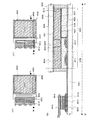
次いで、ゲート絶縁層102、及び酸化物半導体層103上にソース電極層及びドレイン電極層を形成するための導電層の積層を成膜する。
Next, a stack of conductive layers for forming a source electrode layer and a drain electrode layer is formed over the
酸化物半導体層103上に接して第1の金属層を膜厚1nm以上50nm以下で成膜し、その上に第2の金属層としてAl、Cr、Cu、Ta、Ti、Mo、Wから選ばれた元素、または上述した元素を成分とする合金か、上述した元素を組み合わせた合金等からなる導電層を積層して成膜する。
A first metal layer with a thickness of 1 nm to 50 nm is formed in contact with the
本実施の形態では、膜厚1nm以上50nm以下であり、酸化物半導体層よりも薄い錫混合層上に第1のモリブデン層と、アルミニウム層と、第2のモリブデン層とが積層された四層の積層構造とする。材料の異なるターゲットを複数設置できる多元スパッタ装置を用いて、錫のペレットを載せた第1モリブデンターゲットと、ペレットを載せていない第2モリブデンターゲットと、アルミニウムターゲットとを用いて同一チャンバーで大気に触れることなく連続成膜して四層を積層する。なお、四層のうち最も膜厚の薄く、且つ、酸化物半導体層の膜厚よりも薄い層が錫混合層である。連続成膜により、薄い錫混合層の酸化を防ぎ、高抵抗化を防いでいる。 In this embodiment, a four-layer structure in which a first molybdenum layer, an aluminum layer, and a second molybdenum layer are stacked over a tin mixed layer that has a thickness of 1 nm to 50 nm and is thinner than an oxide semiconductor layer. The laminated structure is as follows. Using a multi-source sputtering apparatus in which a plurality of targets of different materials can be installed, the first molybdenum target on which the tin pellets are placed, the second molybdenum target on which the pellets are not placed, and the aluminum target are exposed to the atmosphere in the same chamber. The four layers are stacked by continuous film formation. Note that the tin-mixed layer is the thinnest layer among the four layers and thinner than the oxide semiconductor layer. Continuous film formation prevents oxidation of the thin tin mixed layer and prevents high resistance.
本実施の形態では、ソース電極層及びドレイン電極層の積層のうち酸化物半導体層と接する層として、錫混合層を用いる例を示したが、特に限定されず、Sb、Se、Te、Pd、Ag、Ni、Cu、Pt、Auから選ばれた元素を少なくとも一つを用いる。 In this embodiment, the example in which the tin mixed layer is used as the layer in contact with the oxide semiconductor layer in the stack of the source electrode layer and the drain electrode layer is described; however, there is no particular limitation, and Sb, Se, Te, Pd, At least one element selected from Ag, Ni, Cu, Pt, and Au is used.
次いで、フォトマスクを用いてフォトリソグラフィ工程により、ソース電極層及びドレイン電極層を形成するための四層の積層を選択的にエッチングして、積層からなるソース電極層104a、105aまたはドレイン電極層104b、105bを形成する(図1(B)参照。)。なお、ソース電極層またはドレイン電極層のうち、酸化物半導体層103上に接する錫混合層が104a、104bに相当する。また、このとき酸化物半導体層103も一部がエッチングされ、溝部(凹部)を有する酸化物半導体層103となる。なお、酸化物半導体層103の材料や、ソース電極層及びドレイン電極層の材料や、エッチング条件によっては、酸化物半導体層103に溝部(凹部)が形成されない場合もある。例えば、ソース電極層及びドレイン電極層の積層のうち酸化物半導体層と接する層として、AuやPtを用いる場合、エッチングストッパーとしても機能させることができる。
Next, a four-layer stack for forming the source electrode layer and the drain electrode layer is selectively etched by a photolithography process using a photomask, so that the
次に、ゲート絶縁層102、酸化物半導体層103、ソース電極層104a、105a及びドレイン電極層104b、105bを覆い、酸化物半導体層103の一部と接する保護絶縁層107を形成する(図1(C)参照。)。保護絶縁層107は、少なくとも1nm以上の厚さとし、CVD法、スパッタリング法など、保護絶縁層107に水、水素等の不純物を混入させない方法を適宜用いて成膜することができる。ここでは、保護絶縁層107は、例えばスパッタリング法の一種である、リアクティブスパッタリング法を用いて成膜する。酸化物半導体層103の一部と接して形成される保護絶縁層107は、水分や、水素イオンや、OH−などの不純物を含まず、これらが外部から侵入することをブロックする無機絶縁層を用い、代表的には酸化珪素層、窒化酸化珪素層、窒化珪素層、酸化アルミニウム層、酸化窒化アルミニウム層又は窒化アルミニウム層、を用いることができる。
Next, the protective insulating
また、保護絶縁層107は、酸化珪素層、窒化酸化珪素層、酸化アルミニウム層又は酸化窒化アルミニウム層の上に窒化珪素層又は窒化アルミニウム層を積層する構造としてもよい。特に窒化珪素層は水分や、水素イオンや、OH−などの不純物を含まず、これらが外部から侵入することをブロックしやすいので好ましい。
The protective
保護絶縁層107の成膜時の基板温度は、室温以上300℃以下とすればよく、酸化珪素層のスパッタリング法による成膜は、希ガス(代表的にはアルゴン)雰囲気下、酸素雰囲気下、または希ガス(代表的にはアルゴン)及び酸素混合雰囲気下において行うことができる。また、ターゲットとして酸化珪素ターゲットまたは珪素ターゲットを用いることができる。例えば、珪素ターゲットを用いて、酸素及び希ガス雰囲気下でスパッタリング法により酸化珪素層を形成することができる。本実施の形態では、保護絶縁層107として、珪素ターゲットを用いて成膜する膜厚300nmの酸化珪素層を用いる。
The substrate temperature at the time of forming the protective insulating
以上の工程より、絶縁表面を有する基板である基板100上にゲート電極層101が設けられ、ゲート電極層101の上にゲート絶縁層102が設けられ、ゲート絶縁層102の上に酸化物半導体層103が設けられ、酸化物半導体層103の上に積層からなるソース電極層104a、105aまたはドレイン電極層104b、105bが設けられ、ゲート絶縁層102、酸化物半導体層103、ソース電極層104a、105a及びドレイン電極層104b、105bを覆い、酸化物半導体層103の一部と接する保護絶縁層107が設けられている、ボトムゲート型の薄膜トランジスタ150を形成することができる(図1(D)参照。)。
Through the above steps, the
図2は、本実施の形態で示した薄膜トランジスタ150の上面図である。図1(D)は、図2のX1−X2部位の断面構成を示している。図2において、Lはチャネル長を示しており、Wはチャネル幅を示している。また、Aはチャネル幅方向と平行な方向において、酸化物半導体層103がソース電極層105a及びドレイン電極層105bと重ならない領域の長さを示している。Lsはソース電極層105aとゲート電極層101が重なる領域の長さを示しており、Ldはドレイン電極層105bとゲート電極層101が重なる領域の長さを示している。
FIG. 2 is a top view of the
また必要があれば、保護絶縁層107として膜厚300nmの酸化珪素膜を形成した後に、第2の熱処理を100℃以上400℃以下の範囲内で行ってもよい。本実施の形態では、基板温度を150℃とし、10時間の加熱を行う。この第2の熱処理により、信頼性の高い薄膜トランジスタを作製することができる。
If necessary, a second heat treatment may be performed in the range of 100 ° C. to 400 ° C. after forming a silicon oxide film with a thickness of 300 nm as the protective insulating
また、第2の熱処理のタイミングは、保護絶縁層107形成直後に限定されず、その上に配線や電極(例えば画素電極など)を形成した後に行ってもよい。
The timing of the second heat treatment is not limited to immediately after the protective insulating
また、本実施の形態では、図1(D)に示すボトムゲート型の薄膜トランジスタ150の作製方法について説明したが、本実施の形態の構成はこれに限られるものではない。図3(A)に示すような、ボトムゲート構造のボトムコンタクト型(逆コプラナ型とも呼ぶ)の薄膜トランジスタ160や、図3(B)に示すような、チャネル保護層110を有するチャネル保護型(チャネルストップ型ともいう)の薄膜トランジスタ170等も同様の材料、方法を用いて形成することができる。図3(C)は、チャネルエッチ型薄膜トランジスタの他の例を示している。図3(C)に示す薄膜トランジスタ180は、ゲート電極層101が酸化物半導体層103の端部よりも外側に伸びた構造となっている。
In this embodiment, the method for manufacturing the bottom-gate
また、フォトリソグラフィ工程で用いるフォトマスク数及び工程数を削減するため、透過した光が複数の強度となる露光マスクである多階調マスクによって形成されたレジストマスクを用いてエッチング工程を行ってもよい。多階調マスクを用いて形成したレジストマスクは複数の膜厚を有する形状となり、エッチングを行うことでさらに形状を変形することができるため、異なるパターンに加工する複数のエッチング工程に用いることができる。よって、一枚の多階調マスクによって、少なくとも二種類以上の異なるパターンに対応するレジストマスクを形成することができる。よって露光マスク数を削減することができ、対応するフォトリソグラフィ工程も削減できるため、工程の簡略化が可能となる。 In order to reduce the number of photomasks used in the photolithography process and the number of processes, the etching process may be performed using a resist mask formed by a multi-tone mask that is an exposure mask in which transmitted light has a plurality of intensities. Good. A resist mask formed using a multi-tone mask has a shape with a plurality of thicknesses, and the shape can be further deformed by etching. Therefore, the resist mask can be used for a plurality of etching processes for processing into different patterns. . Therefore, a resist mask corresponding to at least two kinds of different patterns can be formed by using one multi-tone mask. Therefore, the number of exposure masks can be reduced, and the corresponding photolithography process can be reduced, so that the process can be simplified.
なお、薄膜トランジスタのチャネル長(図2中のL)は、ソース電極層105aとドレイン電極層105bとの距離で定義されるが、チャネル保護型の薄膜トランジスタのチャネル長は、キャリアの流れる方向と平行な方向のチャネル保護層の幅で定義される。
Note that the channel length (L in FIG. 2) of the thin film transistor is defined by the distance between the
(実施の形態2)
本実施の形態では、薄膜トランジスタを作製し、該薄膜トランジスタを画素部、さらには駆動回路に用いて表示機能を有する半導体装置(表示装置ともいう)を作製する場合について説明する。また、駆動回路の一部または全体の薄膜トランジスタを、画素部のトランジスタと同じ基板上に形成し、システムオンパネルを形成することができる。
(Embodiment 2)
In this embodiment, the case where a thin film transistor is manufactured and a semiconductor device having a display function (also referred to as a display device) is manufactured using the thin film transistor in a pixel portion and further in a driver circuit will be described. In addition, part or all of the thin film transistors of the driver circuit can be formed over the same substrate as the transistors in the pixel portion, so that a system-on-panel can be formed.
表示装置は表示素子を含む。表示素子としては液晶素子(液晶表示素子ともいう)、発光素子(発光表示素子ともいう)を用いることができる。発光素子は、電流または電圧によって輝度が制御される素子をその範疇に含んでおり、具体的には無機EL(Electro Luminescence)、有機EL等が含まれる。また、電子インクなど、電気的作用によりコントラストが変化する表示媒体も適用することができる。 The display device includes a display element. As the display element, a liquid crystal element (also referred to as a liquid crystal display element) or a light-emitting element (also referred to as a light-emitting display element) can be used. The light-emitting element includes, in its category, an element whose luminance is controlled by current or voltage, and specifically includes inorganic EL (Electro Luminescence), organic EL, and the like. In addition, a display medium whose contrast is changed by an electric effect, such as electronic ink, can be used.
また、表示装置は、表示素子が封止された状態にあるパネルと、該パネルにコントローラを含むIC等を実装した状態にあるモジュールとを含む。さらに表示装置は、該表示装置を作製する過程における、表示素子が完成する前の一形態に相当する素子基板に関し、該素子基板は、電流を表示素子に供給するための手段を複数の各画素に備える。素子基板は、具体的には、表示素子の画素電極のみが形成された状態であっても良いし、画素電極となる導電層を形成した後であって、エッチングして画素電極を形成する前の状態であっても良いし、あらゆる形態があてはまる。 The display device includes a panel in which the display element is sealed, and a module in which an IC including a controller is mounted on the panel. Furthermore, the display device relates to an element substrate which corresponds to one mode before the display element is completed in the process of manufacturing the display device, and the element substrate includes a unit for supplying current to the display element. Prepare for. Specifically, the element substrate may be in a state in which only the pixel electrode of the display element is formed, or after the formation of the conductive layer to be the pixel electrode and before the pixel electrode is formed by etching. It can be in any state, and all forms apply.
なお、本明細書中における表示装置とは、画像表示デバイス、表示デバイス、もしくは光源(照明装置含む)を指す。また、コネクター、例えばFPC(Flexible printed circuit)もしくはTAB(Tape Automated Bonding)テープもしくはTCP(Tape Carrier Package)が取り付けられたモジュール、TABテープやTCPの先にプリント配線板が設けられたモジュール、または表示素子にCOG(Chip On Glass)方式によりIC(集積回路)が直接実装されたモジュールも全て表示装置に含むものとする。 Note that a display device in this specification means an image display device, a display device, or a light source (including a lighting device). Also, a connector, for example, a module with a FPC (Flexible printed circuit) or TAB (Tape Automated Bonding) tape or TCP (Tape Carrier Package), a module with a printed wiring board at the end of a TAB tape or TCP, or a display It is assumed that the display device includes all modules in which an IC (integrated circuit) is directly mounted on the element by a COG (Chip On Glass) method.
本実施の形態では、本発明の一形態である半導体装置として液晶表示装置の例を示す。まず、半導体装置の一形態に相当する液晶表示パネルの外観及び断面について、図4を用いて説明する。図4(A1)(A2)は、第1の基板4001上に形成されたIn−Ga−Zn−O系層を半導体層として含む薄膜トランジスタ4010、4011、及び液晶素子4013を、第2の基板4006との間にシール材4005によって封止した、パネルの上面図であり、図4(B)は、図4(A1)(A2)のM−Nにおける断面図に相当する。
In this embodiment, an example of a liquid crystal display device is described as a semiconductor device which is one embodiment of the present invention. First, the appearance and cross section of a liquid crystal display panel, which is one embodiment of a semiconductor device, will be described with reference to FIGS. 4A1 and 4A2 illustrate
第1の基板4001上に設けられた画素部4002と、走査線駆動回路4004とを囲むようにして、シール材4005が設けられている。また画素部4002と、走査線駆動回路4004の上に第2の基板4006が設けられている。よって画素部4002と、走査線駆動回路4004とは、第1の基板4001とシール材4005と第2の基板4006とによって、液晶層4008と共に封止されている。また第1の基板4001上のシール材4005によって囲まれている領域とは異なる領域に、別途用意された基板上に単結晶半導体又は多結晶半導体で形成された信号線駆動回路4003が実装されている。
A
なお、別途形成した駆動回路の接続方法は、特に限定されるものではなく、COG法、ワイヤボンディング法、或いはTAB法などを用いることができる。図4(A1)は、COG法により信号線駆動回路4003を実装する例であり、図4(A2)は、TAB法により信号線駆動回路4003を実装する例である。
Note that a connection method of a driver circuit which is separately formed is not particularly limited, and a COG method, a wire bonding method, a TAB method, or the like can be used. 4A1 illustrates an example in which the signal
また、第1の基板4001上に設けられた画素部4002と、走査線駆動回路4004は、薄膜トランジスタを複数有しており、図4(B)では、画素部4002に含まれる薄膜トランジスタ4010と、走査線駆動回路4004に含まれる薄膜トランジスタ4011とを例示している。薄膜トランジスタ4010、4011上には絶縁層4020、4021が設けられている。
In addition, the
薄膜トランジスタ4010、4011は、実施の形態1で示した酸化物半導体層を含む薄膜トランジスタを適用することができる。なお、本実施の形態では、薄膜トランジスタ4010、4011のソース電極層またはドレイン電極層は、Cu層とタングステン層との積層であり、Cu層が酸化物半導体層と接する積層構造である。本実施の形態において、薄膜トランジスタ4010、4011はnチャネル型薄膜トランジスタである。
The thin film transistors including the oxide semiconductor layer described in Embodiment 1 can be applied to the
絶縁層4021上において、駆動回路用の薄膜トランジスタ4011の酸化物半導体層のチャネル形成領域と重なる位置に導電層4040が設けられている。導電層4040を酸化物半導体層のチャネル形成領域と重なる位置に設けることによって、BT試験前後における薄膜トランジスタ4011のしきい値電圧の変化量を低減することができる。また、駆動回路用の薄膜トランジスタ4011と重なる位置に導電層4040を設けることによって静電遮断し、ノーマリーオフの薄膜トランジスタとすることもできる。静電遮断とは外部の電場を遮蔽すること、即ち、外部の電場が内部(TFTなどの回路)に作用しないようにすることをいう。BT試験前後における薄膜トランジスタ4011のしきい値電圧の変化量を低減することができる。また、導電層4040は、電位が薄膜トランジスタ4011のゲート電極層と同じでもよいし、異なっていても良く、第2のゲート電極層として機能させることもできる。また、導電層4040の電位がGND、0V、或いはフローティング状態であってもよい。
A
また、液晶素子4013が有する画素電極層4030は、薄膜トランジスタ4010と電気的に接続されている。そして液晶素子4013の対向電極層4031は第2の基板4006上に形成されている。画素電極層4030と対向電極層4031と液晶層4008とが重なっている部分が、液晶素子4013に相当する。なお、画素電極層4030、対向電極層4031はそれぞれ配向膜として機能する絶縁層4032、4033が設けられ、絶縁層4032、4033を介して液晶層4008を挟持している。
In addition, the
なお、第1の基板4001、第2の基板4006としては、ガラス、金属(代表的にはステンレス)、セラミックス、プラスチックを用いることができる。プラスチックとしては、FRP(Fiberglass−Reinforced Plastics)板、PVF(ポリビニルフルオライド)フィルム、ポリエステルフィルムまたはアクリル樹脂フィルムを用いることができる。また、アルミニウムホイルをPVFフィルムやポリエステルフィルムで挟んだ構造のシートを用いることもできる。
Note that as the
また、4035は絶縁層を選択的にエッチングすることで得られる柱状のスペーサであり、画素電極層4030と対向電極層4031との間の距離(セルギャップ)を制御するために設けられている。なお球状のスペーサを用いていても良い。また、対向電極層4031は、薄膜トランジスタ4010と同一基板上に設けられる共通電位線と電気的に接続される。また、共通接続部を用いて、一対の基板間に配置される導電性粒子を介して対向電極層4031と共通電位線とを電気的に接続することができる。なお、導電性粒子はシール材4005に含有させる。
また、配向膜を用いないブルー相を示す液晶を用いてもよい。ブルー相は液晶相の一つであり、コレステリック液晶を昇温していくと、コレステリック相から等方相へ転移する直前に発現する相である。ブルー相は狭い温度範囲でしか発現しないため、温度範囲を改善するために5重量%以上のカイラル剤を混合させた液晶組成物を用いて液晶層4008に用いる。ブルー相を示す液晶とカイラル剤とを含む液晶組成物は、応答速度が1msec以下と短く、光学的等方性であるため配向処理が不要であり、視野角依存性が小さい。
Alternatively, a liquid crystal exhibiting a blue phase for which an alignment film is unnecessary may be used. The blue phase is one of the liquid crystal phases. When the temperature of the cholesteric liquid crystal is increased, the blue phase appears immediately before the transition from the cholesteric phase to the isotropic phase. Since the blue phase appears only in a narrow temperature range, a liquid crystal composition mixed with 5% by weight or more of a chiral agent is used for the
また、ブルー相を示す液晶を用いると、配向膜へのラビング処理も不要となるため、ラビング処理によって引き起こされる静電破壊を防止することができ、作製工程中の液晶表示装置の不良や破損を軽減することができる。よって液晶表示装置の生産性を向上させることが可能となる。特に、酸化物半導体層を用いる薄膜トランジスタは、静電気の影響により薄膜トランジスタの電気的な特性が著しく変動して設計範囲を逸脱する恐れがある。よって酸化物半導体層を用いる薄膜トランジスタを有する液晶表示装置にブルー相の液晶材料を用いることはより効果的である。 In addition, when a liquid crystal exhibiting a blue phase is used, a rubbing process to the alignment film is not necessary, so that electrostatic breakdown caused by the rubbing process can be prevented, and defects or breakage of the liquid crystal display device during the manufacturing process can be prevented. Can be reduced. Therefore, the productivity of the liquid crystal display device can be improved. In particular, in a thin film transistor using an oxide semiconductor layer, the electrical characteristics of the thin film transistor may significantly fluctuate due to the influence of static electricity and deviate from the design range. Therefore, it is more effective to use a blue phase liquid crystal material for a liquid crystal display device including a thin film transistor using an oxide semiconductor layer.
なお、本実施の形態で示す液晶表示装置は透過型液晶表示装置の例であるが、液晶表示装置は反射型液晶表示装置でも半透過型液晶表示装置でも適用できる。 Note that although the liquid crystal display device described in this embodiment is an example of a transmissive liquid crystal display device, the liquid crystal display device can be applied to a reflective liquid crystal display device or a transflective liquid crystal display device.
また、本実施の形態で示す液晶表示装置では、基板の外側(視認側)に偏光板を設け、内側に着色層、表示素子に用いる電極層という順に設ける例を示すが、偏光板は基板の内側に設けてもよい。また、偏光板と着色層の積層構造も本実施の形態に限定されず、偏光板及び着色層の材料や作製工程条件によって適宜設定すればよい。また、必要に応じてブラックマトリクスとして機能する遮光層を設けてもよい。 In the liquid crystal display device described in this embodiment, a polarizing plate is provided on the outer side (viewing side) of the substrate, a colored layer is provided on the inner side, and an electrode layer used for the display element is provided in this order. It may be provided inside. Further, the stacked structure of the polarizing plate and the colored layer is not limited to this embodiment mode, and may be set as appropriate depending on the material and manufacturing process conditions of the polarizing plate and the colored layer. Further, a light shielding layer that functions as a black matrix may be provided as necessary.
また、本実施の形態では、薄膜トランジスタ起因の表面凹凸を低減するため、及び薄膜トランジスタの信頼性を向上させるため、薄膜トランジスタを保護層や平坦化絶縁層として機能する絶縁層(絶縁層4020、絶縁層4021)で覆う構成となっている。なお、保護層は、大気中に浮遊する有機物や金属物、水蒸気などの汚染不純物の侵入を防ぐためのものであり、緻密な膜が好ましい。保護層は、スパッタ法を用いて、酸化珪素層、窒化珪素層、酸化窒化珪素層、窒化酸化珪素層、酸化アルミニウム層、窒化アルミニウム層、酸化窒化アルミニウム層、又は窒化酸化アルミニウム層の単層、又は積層で成膜すればよい。本実施の形態では保護層をスパッタ法で成膜する例を示すが、特に限定されず種々の方法で成膜すればよい。
In this embodiment, in order to reduce surface unevenness due to the thin film transistor and improve the reliability of the thin film transistor, the thin film transistor is an insulating layer functioning as a protective layer or a planarization insulating layer (the insulating
ここでは、保護層として積層構造の絶縁層4020を形成する。ここでは、絶縁層4020の一層目として、スパッタ法を用いて酸化珪素層を成膜する。保護層として酸化珪素層を用いると、ソース電極層及びドレイン電極層としてアルミニウム層を用いる場合、用いるアルミニウム層のヒロック防止に効果がある。
Here, an insulating
また、保護層の二層目として絶縁層を形成する。ここでは、絶縁層4020の二層目として、スパッタ法を用いて窒化珪素層を成膜する。保護層として窒化珪素層を用いると、ナトリウム等のイオンが半導体領域中に侵入して、TFTの電気特性を変化させることを抑制することができる。
In addition, an insulating layer is formed as a second layer of the protective layer. Here, as the second layer of the insulating
また、平坦化絶縁層として絶縁層4021を形成する。絶縁層4021としては、ポリイミド、アクリル、ベンゾシクロブテン、ポリアミド、エポキシ等の、耐熱性を有する有機材料を用いることができる。また上記有機材料の他に、低誘電率材料(low−k材料)、シロキサン系樹脂、PSG(リンガラス)、BPSG(リンボロンガラス)等を用いることができる。なお、これらの材料で形成される絶縁層を複数積層させることで、絶縁層4021を形成してもよい。
The insulating
なおシロキサン系樹脂とは、シロキサン系材料を出発材料として形成されたSi−O−Si結合を含む樹脂に相当する。シロキサン系樹脂は置換基として有機基(例えばアルキル基やアリール基)やフルオロ基を用いても良い。また、有機基はフルオロ基を有していても良い。 Note that the siloxane-based resin corresponds to a resin including a Si—O—Si bond formed using a siloxane-based material as a starting material. The siloxane-based resin may use an organic group (for example, an alkyl group or an aryl group) or a fluoro group as a substituent. The organic group may have a fluoro group.
絶縁層4021の形成法は、特に限定されず、その材料に応じて、スパッタ法、SOG法、スピンコート、ディップ、スプレー塗布、液滴吐出法(インクジェット法、スクリーン印刷、オフセット印刷等)、ドクターナイフ、ロールコーター、カーテンコーター、ナイフコーター等を用いることができる。絶縁層4021を材料液を用いて形成する場合、ベークする工程で同時に、半導体層のアニール(300℃〜400℃)を行ってもよい。絶縁層4021の焼成工程と半導体層のアニールを兼ねることで効率よく半導体装置を作製することが可能となる。
The formation method of the insulating
画素電極層4030、対向電極層4031は、酸化タングステンを含むインジウム酸化物、酸化タングステンを含むインジウム亜鉛酸化物、酸化チタンを含むインジウム酸化物、酸化チタンを含むインジウム錫酸化物、インジウム錫酸化物、インジウム亜鉛酸化物、酸化ケイ素を添加したインジウム錫酸化物などの透光性を有する導電性材料を用いることができる。
The
また、画素電極層4030、対向電極層4031として、導電性高分子(導電性ポリマーともいう)を含む導電性組成物を用いて形成することができる。導電性組成物を用いて形成した画素電極は、シート抵抗が10000Ω/□以下、波長550nmにおける透光率が70%以上であることが好ましい。また、導電性組成物に含まれる導電性高分子の抵抗率が0.1Ω・cm以下であることが好ましい。
The
導電性高分子としては、いわゆるπ電子共役系導電性高分子を用いることができる。例えば、ポリアニリンまたはその誘導体、ポリピロールまたはその誘導体、ポリチオフェンまたはその誘導体、若しくはこれらの2種以上の共重合体などがあげられる。 As the conductive polymer, a so-called π-electron conjugated conductive polymer can be used. For example, polyaniline or a derivative thereof, polypyrrole or a derivative thereof, polythiophene or a derivative thereof, or a copolymer of two or more kinds thereof can be given.
また別途形成された信号線駆動回路4003と、走査線駆動回路4004または画素部4002に与えられる各種信号及び電位は、FPC4018から供給されている。
In addition, a variety of signals and potentials are supplied to the signal
本実施の形態では、接続端子電極4015が、液晶素子4013が有する画素電極層4030と同じ導電層から形成され、端子電極4016は、薄膜トランジスタ4010、4011のソース電極層及びドレイン電極層と同じ導電層で形成されている。従って、端子電極4016は、Cu層とタングステン層との積層で形成されている。
In this embodiment, the
接続端子電極4015は、FPC4018が有する端子と、異方性導電層4019を介して電気的に接続されている。
The
また図4においては、信号線駆動回路4003を別途形成し、第1の基板4001に実装している例を示しているが、本実施の形態はこの構成に限定されない。走査線駆動回路を別途形成して実装しても良いし、信号線駆動回路の一部または走査線駆動回路の一部のみを別途形成して実装しても良い。
FIG. 4 illustrates an example in which the signal
また、必要であれば、カラーフィルタを各画素に対応して設ける。また、第1の基板4001と第2の基板4006の外側には偏光板や拡散板を設ける。また、バックライトの光源は冷陰極管やLEDにより構成されて液晶表示モジュールとなる。
If necessary, a color filter is provided for each pixel. In addition, a polarizing plate and a diffusion plate are provided outside the
液晶表示モジュールには、TN(Twisted Nematic)モード、IPS(In−Plane−Switching)モード、FFS(Fringe Field Switching)モード、MVA(Multi−domain Vertical Alignment)モード、PVA(Patterned Vertical Alignment)モード、ASM(Axially Symmetric aligned Micro−cell)モード、OCB(Optical Compensated Birefringence)モード、FLC(Ferroelectric Liquid Crystal)モード、AFLC(AntiFerroelectric Liquid Crystal)モードなどを用いることができる。 The liquid crystal display module includes a TN (Twisted Nematic) mode, an IPS (In-Plane-Switching) mode, an FFS (Fringe Field Switching) mode, an MVA (Multi-domain Vertical Alignment) mode, and a PVA (Pattern Vertical Alignment) mode. (Axial Symmetrical Aligned Micro-cell) mode, OCB (Optical Compensated Birefringence) mode, FLC (Ferroelectric Liquid Crystal) mode, AFLC (Anti-Ferroelectric Crystal) mode, etc. It is possible to have.
以上の工程により、電気特性の高い薄膜トランジスタを有する液晶表示装置を作製することができる。 Through the above process, a liquid crystal display device including a thin film transistor with high electrical characteristics can be manufactured.
本実施の形態は、実施の形態1に記載した構成と自由に組み合わせて実施することが可能である。 This embodiment mode can be implemented freely combining with the structure described in Embodiment Mode 1.
(実施の形態3)
半導体装置の一形態として電子ペーパーの例を示す。
(Embodiment 3)
An example of electronic paper will be described as an embodiment of a semiconductor device.
実施の形態1の薄膜トランジスタは、スイッチング素子と電気的に接続する素子を利用して電子インクを駆動させる電子ペーパーに用いてもよい。電子ペーパーは、電気泳動表示装置(電気泳動ディスプレイ)とも呼ばれており、紙と同じ読みやすさ、他の表示装置に比べ低消費電力、薄くて軽い形状とすることが可能という利点を有している。 The thin film transistor of Embodiment 1 may be used for electronic paper in which electronic ink is driven using an element electrically connected to a switching element. Electronic paper is also called an electrophoretic display device (electrophoretic display), and has the same readability as paper, low power consumption compared to other display devices, and the advantage that it can be made thin and light. ing.
電気泳動ディスプレイは、様々な形態が考えられ得るが、プラスの電荷を有する第1の粒子と、マイナスの電荷を有する第2の粒子とを含むマイクロカプセルが溶媒または溶質に複数分散されたものであり、マイクロカプセルに電界を印加することによって、マイクロカプセル中の粒子を互いに反対方向に移動させて一方側に集合した粒子の色のみを表示するものである。なお、第1の粒子または第2の粒子は染料を含み、電界がない場合において移動しないものである。また、第1の粒子の色と第2の粒子の色は異なるもの(無色を含む)とする。 The electrophoretic display can be considered in various forms, and a plurality of microcapsules including first particles having a positive charge and second particles having a negative charge are dispersed in a solvent or a solute. In other words, by applying an electric field to the microcapsules, the particles in the microcapsules are moved in opposite directions to display only the color of the particles assembled on one side. Note that the first particle or the second particle contains a dye and does not move in the absence of an electric field. In addition, the color of the first particles and the color of the second particles are different (including colorless).
このように、電気泳動ディスプレイは、誘電定数の高い物質が高い電界領域に移動する、いわゆる誘電泳動的効果を利用したディスプレイである。 As described above, the electrophoretic display is a display using a so-called dielectrophoretic effect in which a substance having a high dielectric constant moves to a high electric field region.
上記マイクロカプセルを溶媒中に分散させたものが電子インクと呼ばれるものであり、この電子インクはガラス、プラスチック、布、紙などの表面に印刷することができる。また、カラーフィルタや色素を有する粒子を用いることによってカラー表示も可能である。 A solution in which the above microcapsules are dispersed in a solvent is referred to as electronic ink. This electronic ink can be printed on a surface of glass, plastic, cloth, paper, or the like. Color display is also possible by using particles having color filters or pigments.
また、アクティブマトリクス基板上に適宜、二つの電極の間に挟まれるように上記マイクロカプセルを複数配置すればアクティブマトリクス型の表示装置が完成し、マイクロカプセルに電界を印加すれば表示を行うことができる。例えば、実施の形態1の薄膜トランジスタによって得られるアクティブマトリクス基板を用いることができる。 In addition, an active matrix display device can be completed by arranging a plurality of the above microcapsules so as to be appropriately sandwiched between two electrodes on an active matrix substrate, and display can be performed by applying an electric field to the microcapsules. it can. For example, an active matrix substrate obtained by the thin film transistor of Embodiment 1 can be used.
なお、マイクロカプセル中の第1の粒子および第2の粒子は、導電体材料、絶縁体材料、半導体材料、磁性材料、液晶材料、強誘電性材料、エレクトロルミネセント材料、エレクトロクロミック材料、磁気泳動材料から選ばれた一種の材料、またはこれらの複合材料を用いればよい。 Note that the first particle and the second particle in the microcapsule are a conductor material, an insulator material, a semiconductor material, a magnetic material, a liquid crystal material, a ferroelectric material, an electroluminescent material, an electrochromic material, or a magnetophoresis. A kind of material selected from the materials or a composite material thereof may be used.
図5は、半導体装置の例としてアクティブマトリクス型の電子ペーパーを示す。半導体装置に用いられる薄膜トランジスタ581としては、実施の形態1で示す薄膜トランジスタと同様に作製でき、ソース電極層またはドレイン電極層として酸化物半導体層に接する錫混合層を含む積層を有する薄膜トランジスタである。
FIG. 5 illustrates active matrix electronic paper as an example of a semiconductor device. A
図5の電子ペーパーは、ツイストボール表示方式を用いた表示装置の例である。ツイストボール表示方式とは、白と黒に塗り分けられた球形粒子を表示素子に用いる電極層である第1の電極層及び第2の電極層の間に配置し、第1の電極層及び第2の電極層に電位差を生じさせての球形粒子の向きを制御することにより、表示を行う方法である。 The electronic paper in FIG. 5 is an example of a display device using a twisting ball display system. The twist ball display method is a method in which spherical particles separately painted in white and black are arranged between a first electrode layer and a second electrode layer which are electrode layers used for a display element, and the first electrode layer and the second electrode layer are arranged. In this method, display is performed by controlling the orientation of spherical particles by generating a potential difference between the two electrode layers.
薄膜トランジスタ581はボトムゲート構造の薄膜トランジスタであり、半導体層と接する絶縁層583に覆われている。薄膜トランジスタ581のソース電極層又はドレイン電極層は第1の電極層587と、絶縁層583、585に形成する開口で接しており電気的に接続している。第1の電極層587と第2の電極層588との間には黒色領域590a及び白色領域590bを有し、周りに液体で満たされているキャビティ594を含む球形粒子589が設けられており、球形粒子589の周囲は樹脂等の充填材595で充填されている(図5参照。)。第1の電極層587が画素電極に相当し、第2の電極層588が共通電極に相当する。第2の電極層588は、薄膜トランジスタ581と同一基板上に設けられる共通電位線と電気的に接続される。共通接続部において、基板580と基板596の間に配置される導電性粒子を介して第2の電極層588と共通電位線とを電気的に接続することができる。
The
また、ツイストボールの代わりに、電気泳動素子を用いることも可能である。透明な液体と、正に帯電した白い微粒子と負に帯電した黒い微粒子とを封入した直径10μm〜200μm程度のマイクロカプセルを用いる。第1の電極層と第2の電極層との間に設けられるマイクロカプセルは、第1の電極層と第2の電極層によって、電場が与えられると、白い微粒子と、黒い微粒子が互いに逆の方向に移動し、白または黒を表示することができる。この原理を応用した表示素子が電気泳動表示素子であり、一般的に電子ペーパーとよばれている。電気泳動表示素子は、液晶表示素子に比べて反射率が高いため、補助ライトは不要であり、また消費電力が小さく、薄暗い場所でも表示部を認識することが可能である。また、表示部に電源が供給されない場合であっても、一度表示した像を保持することが可能であるため、電波発信源から表示機能付き半導体装置(単に表示装置、又は表示装置を具備する半導体装置ともいう)を遠ざけた場合であっても、表示された像を保存しておくことが可能となる。 Further, instead of the twisting ball, an electrophoretic element can be used. A microcapsule having a diameter of about 10 μm to 200 μm in which transparent liquid, positively charged white microparticles, and negatively charged black microparticles are enclosed is used. In the microcapsule provided between the first electrode layer and the second electrode layer, when an electric field is applied by the first electrode layer and the second electrode layer, the white particles and the black particles are opposite to each other. Move in the direction and can display white or black. A display element using this principle is an electrophoretic display element, and is generally called electronic paper. Since the electrophoretic display element has higher reflectance than the liquid crystal display element, an auxiliary light is unnecessary, power consumption is small, and the display portion can be recognized even in a dim place. Further, even when power is not supplied to the display portion, an image once displayed can be held; therefore, a semiconductor device with a display function from a radio wave source (simply a display device or a semiconductor having a display device) Even when the device is also moved away, the displayed image can be stored.
以上の工程により、電気特性の高い薄膜トランジスタを有する電子ペーパーを作製することができる。 Through the above steps, an electronic paper including a thin film transistor with high electrical characteristics can be manufactured.
本実施の形態は、実施の形態1に記載した構成と適宜組み合わせて実施することが可能である。 This embodiment can be implemented in appropriate combination with the structure described in Embodiment 1.
(実施の形態4)
半導体装置の一形態に相当する発光表示パネル(発光パネルともいう)の外観及び断面について、図6を用いて説明する。図6(A)は、第1の基板上に形成された薄膜トランジスタ及び発光素子を、第2の基板との間にシール材によって封止した、パネルの平面図であり、図6(B)は、図6(A)のH−Iにおける断面図に相当する。
(Embodiment 4)
The appearance and a cross section of a light-emitting display panel (also referred to as a light-emitting panel), which is one embodiment of a semiconductor device, will be described with reference to FIGS. 6A is a plan view of a panel in which a thin film transistor and a light-emitting element formed over a first substrate are sealed with a sealant between the second substrate and FIG. 6B. 6 corresponds to a cross-sectional view taken along line HI in FIG.
第1の基板4501上に設けられた画素部4502、信号線駆動回路4503a、4503b、及び走査線駆動回路4504a、4504bを囲むようにして、シール材4505が設けられている。また画素部4502、信号線駆動回路4503a、4503b、及び走査線駆動回路4504a、4504bの上に第2の基板4506が設けられている。よって画素部4502、信号線駆動回路4503a、4503b、及び走査線駆動回路4504a、4504bは、第1の基板4501とシール材4505と第2の基板4506とによって、充填材4507と共に密封されている。このように外気に曝されないように気密性が高く、脱ガスの少ない保護フィルム(貼り合わせフィルム、紫外線硬化樹脂フィルム等)やカバー材でパッケージング(封入)することが好ましい。
A
また第1の基板4501上に設けられた画素部4502、信号線駆動回路4503a、4503b、及び走査線駆動回路4504a、4504bは、薄膜トランジスタを複数有しており、図6(B)では、画素部4502に含まれる薄膜トランジスタ4510と、信号線駆動回路4503aに含まれる薄膜トランジスタ4509とを例示している。
In addition, the
薄膜トランジスタ4509、4510は、実施の形態1で示した酸化物半導体層に接する錫混合層を有する薄膜トランジスタを適用することができる。なお、薄膜トランジスタ4509、4510のソース電極層またはドレイン電極層は、錫混合層とモリブデン層との積層であり、錫混合層が酸化物半導体層と接する積層構造である。本実施の形態において、薄膜トランジスタ4509、4510はnチャネル型薄膜トランジスタである。
As the
絶縁層4544上において駆動回路用の薄膜トランジスタ4509の酸化物半導体層のチャネル形成領域と重なる位置に導電層4540が設けられている。導電層4540を少なくとも酸化物半導体層のチャネル形成領域と重なる位置に設けることによって、BT試験前後における薄膜トランジスタ4509のしきい値電圧の変化量を低減することができる。また、駆動回路用の薄膜トランジスタ4509と重なる位置に導電層4540を設けることによって静電遮蔽し、ノーマリーオフの薄膜トランジスタとすることもできる。また、導電層4540は、電位が薄膜トランジスタ4509のゲート電極層と同じでもよいし、異なっていても良く、第2のゲート電極層として機能させることもできる。また、導電層4540の電位がGND、0V、或いはフローティング状態であってもよい。
A
薄膜トランジスタ4509は、保護絶縁層としてチャネル形成領域を含む半導体層に接して絶縁層4541が形成されている。絶縁層4541は実施の形態1で示した保護絶縁層107と同様な材料及び方法で形成すればよい。また、薄膜トランジスタ起因の表面凹凸を低減するため平坦化絶縁層として機能する絶縁層4544で覆う構成となっている。ここでは、絶縁層4541として、実施の形態1に示す保護絶縁層107と同様にスパッタ法により酸化珪素層を成膜する。
In the
また、絶縁層4541上に保護絶縁層4542が形成されている。保護絶縁層4542は実施の形態1で示した保護絶縁層107と同様な材料及び方法で形成すればよい。ここでは、保護絶縁層4542として、PCVD法により窒化珪素層を成膜する。
In addition, a protective insulating
また、平坦化絶縁層として絶縁層4544を形成する。絶縁層4544としては、実施の形態2で示した絶縁層4021と同様な材料及び方法で形成すればよい。ここでは、絶縁層4544としてアクリルを用いる。
In addition, an insulating
また4511は発光素子に相当し、発光素子4511が有する画素電極である第1の電極層4517は、薄膜トランジスタ4510のソース電極層またはドレイン電極層と電気的に接続されている。なお発光素子4511の構成は、第1の電極層4517、電界発光層4512、第2の電極層4513の積層構造であるが、示した構成に限定されない。発光素子4511から取り出す光の方向などに合わせて、発光素子4511の構成は適宜変えることができる。
4511 corresponds to a light-emitting element, and a
また、絶縁層4544に代えてカラーフィルタ層を設ける構成としてもよい。フルカラー表示を行う場合、例えば発光素子4511として緑色発光素子とし、隣り合う一方の発光素子を赤色発光素子とし、もう一方の発光素子を青色発光素子とする。また、3種類の発光素子だけでなく白色素子を加えた4種類の発光素子でフルカラー表示ができる発光表示装置を作製してもよい。また、配置する複数の発光素子を全て白色発光素子として、発光素子4511上方にカラーフィルタなどを有する封止基板を配置する構成とし、フルカラー表示ができる発光表示装置を作製してもよい。白色などの単色の発光を示す材料を形成し、カラーフィルタや色変換層を組み合わせることによりフルカラー表示を行うことができる。また、フルカラー表示を行うため、赤色の発光素子、青色の発光素子、及び緑色の発光素子を画素部に用いた表示装置を作製してもよい。もちろん単色発光の表示を行ってもよい。例えば、白色発光を発光する発光素子を用いて発光表示装置を照明装置としてもよいし、他の単色発光を発光する発光素子を用いてエリアカラータイプの照明装置を形成してもよい。
Alternatively, a color filter layer may be provided instead of the insulating
隔壁4520は、有機樹脂層、無機絶縁層または有機ポリシロキサンを用いて形成する。特に感光性の材料を用い、第1の電極層4517上に開口部を形成し、その開口部の側壁が連続した曲率を持って形成される傾斜面となるように形成することが好ましい。
A
電界発光層4512は、単数の層で構成されていても、複数の層が積層されるように構成されていてもどちらでも良い。
The
発光素子4511に酸素、水素、水分、二酸化炭素等が侵入しないように、第2の電極層4513及び隔壁4520上に保護層を形成してもよい。保護層としては、窒化珪素層、窒化酸化珪素層、DLC層等を形成することができる。
A protective layer may be formed over the
また、信号線駆動回路4503a、4503b、走査線駆動回路4504a、4504b、または画素部4502に与えられる各種信号及び電位は、FPC4518a、4518bから供給されている。
In addition, a variety of signals and potentials are supplied to the signal
接続端子電極4515が、発光素子4511が有する第1の電極層4517と同じ導電層から形成され、端子電極4516は、薄膜トランジスタ4509、4510が有するソース電極層及びドレイン電極層と同じ導電層から形成されている。従って、端子電極4516は、錫混合層4514とモリブデン層との積層で形成されている。
The
接続端子電極4515は、FPC4518aが有する端子と、異方性導電層4519を介して電気的に接続されている。
The
発光素子4511からの光の取り出し方向に位置する基板である第2の基板は透光性でなければならない。その場合には、ガラス板、プラスチック板、ポリエステルフィルムまたはアクリルフィルムのような透光性を有する材料を用いる。
The second substrate which is a substrate positioned in the direction in which light is extracted from the
また、充填材4507としては窒素やアルゴンなどの不活性な気体の他に、紫外線硬化樹脂または熱硬化樹脂を用いることができ、PVC(ポリビニルクロライド)、アクリル、ポリイミド、エポキシ樹脂、シリコーン樹脂、PVB(ポリビニルブチラル)またはEVA(エチレンビニルアセテート)を用いることができる。例えば充填材として窒素を用いればよい。
In addition to inert gas such as nitrogen and argon, an ultraviolet curable resin or a thermosetting resin can be used as the
また、必要であれば、発光素子の射出面に偏光板、又は円偏光板(楕円偏光板を含む)、位相差板(λ/4板、λ/2板)、カラーフィルタなどの光学フィルムを適宜設けてもよい。また、偏光板又は円偏光板に反射防止膜を設けてもよい。例えば、表面の凹凸により反射光を拡散し、映り込みを低減できるアンチグレア処理を施すことができる。 If necessary, an optical film such as a polarizing plate, a circular polarizing plate (including an elliptical polarizing plate), a retardation plate (λ / 4 plate, λ / 2 plate), a color filter, or the like is provided on the light emitting element exit surface. You may provide suitably. Further, an antireflection film may be provided on the polarizing plate or the circularly polarizing plate. For example, anti-glare treatment can be performed that diffuses reflected light due to surface irregularities and reduces reflection.
信号線駆動回路4503a、4503b、及び走査線駆動回路4504a、4504bは、別途用意された基板上に単結晶半導体又は多結晶半導体によって形成された駆動回路で実装されていてもよい。また、信号線駆動回路のみ、或いはその一部、又は走査線駆動回路のみ、或いはその一部のみを別途形成して実装しても良く、図6の構成に限定されない。
The signal
以上の工程により、電気特性の高い薄膜トランジスタを有する発光表示装置(表示パネル)を作製することができる。 Through the above process, a light-emitting display device (display panel) including a thin film transistor with high electrical characteristics can be manufactured.
本実施の形態は、実施の形態1に記載した構成と適宜組み合わせて実施することが可能である。 This embodiment can be implemented in appropriate combination with the structure described in Embodiment 1.
(実施の形態5)
本明細書に開示する半導体装置は、さまざまな電子機器(遊技機も含む)に適用することができる。電子機器としては、例えば、テレビジョン装置(テレビ、またはテレビジョン受信機ともいう)、コンピュータ用などのモニタ、デジタルカメラ、デジタルビデオカメラ、デジタルフォトフレーム、携帯電話機(携帯電話、携帯電話装置ともいう)、携帯型ゲーム機、携帯情報端末、音響再生装置、パチンコ機などの大型ゲーム機、太陽電池などが挙げられる。
(Embodiment 5)
The semiconductor device disclosed in this specification can be applied to a variety of electronic devices (including game machines). Examples of the electronic device include a television device (also referred to as a television or a television receiver), a monitor for a computer, a digital camera, a digital video camera, a digital photo frame, a mobile phone (also referred to as a mobile phone or a mobile phone device). ), Large game machines such as portable game machines, portable information terminals, sound reproducing devices, and pachinko machines, solar batteries, and the like.
図7(A)は、携帯電話機の一例を示している。携帯電話機1100は、筐体1101に組み込まれた表示部1102の他、操作ボタン1103、外部接続ポート1104、スピーカ1105、マイク1106などを備えている。
FIG. 7A illustrates an example of a mobile phone. A
図7(A)に示す携帯電話機1100は、表示部1102を指などで触れることで、情報を入力することができる。また、電話を掛ける、或いはメールを打つなどの操作は、表示部1102を指などで触れることにより行うことができる。
A
表示部1102の画面は主として3つのモードがある。第1は、画像の表示を主とする表示モードであり、第2は、文字等の情報の入力を主とする入力モードである。第3は表示モードと入力モードの2つのモードが混合した表示+入力モードである。
There are mainly three screen modes of the
例えば、電話を掛ける、或いはメールを作成する場合は、表示部1102を文字の入力を主とする文字入力モードとし、画面に表示させた文字の入力操作を行えばよい。この場合、表示部1102の画面のほとんどにキーボードまたは番号ボタンを表示させることが好ましい。
For example, when making a phone call or creating an e-mail, the
また、携帯電話機1100内部に、ジャイロ、加速度センサ等の傾きを検出するセンサを有する検出装置を設けることで、携帯電話機1100の向き(縦か横か)を判断して、表示部1102の画面表示を自動的に切り替えるようにすることができる。
In addition, the
また、画面モードの切り替えは、表示部1102を触れること、又は筐体1101の操作ボタン1103の操作により行われる。また、表示部1102に表示される画像の種類によって切り替えるようにすることもできる。例えば、表示部に表示する画像信号が動画のデータであれば表示モード、テキストデータであれば入力モードに切り替える。
The screen mode is switched by touching the
また、入力モードにおいて、表示部1102の光センサで検出される信号を検知し、表示部1102のタッチ操作による入力が一定期間ない場合には、画面のモードを入力モードから表示モードに切り替えるように制御してもよい。
Further, in the input mode, when a signal detected by the optical sensor of the
表示部1102は、イメージセンサとして機能させることもできる。例えば、表示部1102に掌や指を触れることで、掌紋、指紋等を撮像することで、本人認証を行うことができる。また、表示部に近赤外光を発光するバックライトまたは近赤外光を発光するセンシング用光源を用いれば、指静脈、掌静脈などを撮像することもできる。
The
表示部1102には、画素のスイッチング素子として、実施の形態1に示す薄膜トランジスタを複数配置する。
In the
図7(B)も携帯型情報端末の一例である。図7(B)を一例とした携帯型情報端末は、複数の機能を備えることができる。例えば電話機能に加えて、コンピュータを内蔵し、様々なデータ処理機能を備えることもできる。 FIG. 7B is also an example of a portable information terminal. A portable information terminal whose example is illustrated in FIG. 7B can include a plurality of functions. For example, in addition to the telephone function, a computer can be built in and various data processing functions can be provided.
図7(B)に示す携帯型情報端末は、筐体2800及び筐体2801の二つの筐体で構成されている。筐体2801には、表示パネル2802、スピーカ2803、マイクロフォン2804、ポインティングデバイス2806、カメラ用レンズ2807、外部接続端子2808などを備えている。また、筐体2800には、携帯型情報端末の充電を行う太陽電池セル2810、外部メモリスロット2811などを備えている。また、アンテナは筐体2801内部に内蔵されている。
A portable information terminal illustrated in FIG. 7B includes two housings, a
また、表示パネル2802はタッチパネルを備えており、図7(B)には映像表示されている複数の操作キー2805を点線で示している。
Further, the
また、上記構成に加えて、非接触ICチップ、小型記録装置などを内蔵していてもよい。 In addition to the above structure, a non-contact IC chip, a small recording device, or the like may be incorporated.
発光装置は、表示パネル2802に用いることができ、使用形態に応じて表示の方向が適宜変化する。また、表示パネル2802と同一面上にカメラ用レンズ2807を備えているため、テレビ電話が可能である。スピーカ2803及びマイクロフォン2804は音声通話に限らず、テレビ電話、録音、再生などが可能である。さらに、筐体2800と筐体2801は、スライドし、図7(B)のように展開している状態から重なり合った状態とすることができ、携帯に適した小型化が可能である。
The light-emitting device can be used for the
外部接続端子2808はACアダプタ及びUSBケーブルなどの各種ケーブルと接続可能であり、充電及びパーソナルコンピュータなどとのデータ通信が可能である。また、外部メモリスロット2811に記録媒体を挿入し、より大量のデータ保存及び移動に対応できる。
The
また、上記機能に加えて、赤外線通信機能、テレビ受信機能などを備えたものであってもよい。 In addition to the above functions, an infrared communication function, a television reception function, or the like may be provided.
図8(A)は、テレビジョン装置の一例を示している。テレビジョン装置9600は、筐体9601に表示部9603が組み込まれている。表示部9603により、映像を表示することが可能である。また、ここでは、スタンド9605により筐体9601を支持した構成を示している。
FIG. 8A illustrates an example of a television device. In the
テレビジョン装置9600の操作は、筐体9601が備える操作スイッチや、別体のリモコン操作機9610により行うことができる。リモコン操作機9610が備える操作キー9609により、チャンネルや音量の操作を行うことができ、表示部9603に表示される映像を操作することができる。また、リモコン操作機9610に、当該リモコン操作機9610から出力する情報を表示する表示部9607を設ける構成としてもよい。
The
なお、テレビジョン装置9600は、受信機やモデムなどを備えた構成とする。受信機により一般のテレビ放送の受信を行うことができ、さらにモデムを介して有線または無線による通信ネットワークに接続することにより、一方向(送信者から受信者)または双方向(送信者と受信者間、あるいは受信者間同士など)の情報通信を行うことも可能である。
Note that the
表示部9603には、画素のスイッチング素子として、実施の形態1に示す薄膜トランジスタを複数配置する。
In the
図8(B)は、デジタルフォトフレームの一例を示している。例えば、デジタルフォトフレーム9700は、筐体9701に表示部9703が組み込まれている。表示部9703は、各種画像を表示することが可能であり、例えばデジタルカメラなどで撮影した画像データを表示させることで、通常の写真立てと同様に機能させることができる。
FIG. 8B illustrates an example of a digital photo frame. For example, a
表示部9703には、画素のスイッチング素子として、実施の形態1に示す薄膜トランジスタを複数配置する。
In the
なお、デジタルフォトフレーム9700は、操作部、外部接続用端子(USB端子、USBケーブルなどの各種ケーブルと接続可能な端子など)、記録媒体挿入部などを備える構成とする。これらの構成は、表示部と同一面に組み込まれていてもよいが、側面や裏面に備えるとデザイン性が向上するため好ましい。例えば、デジタルフォトフレームの記録媒体挿入部に、デジタルカメラで撮影した画像データを記憶したメモリを挿入して画像データを取り込み、取り込んだ画像データを表示部9703に表示させることができる。
Note that the
また、デジタルフォトフレーム9700は、無線で情報を送受信できる構成としてもよい。無線により、所望の画像データを取り込み、表示させる構成とすることもできる。
Further, the
図9は、実施の形態4を適用して形成される発光装置を、室内の照明装置3001として用いた例である。実施の形態4で示した発光装置は大面積化も可能であるため、大面積の照明装置として用いることができる。また、実施の形態4で示した発光装置は、卓上照明器具3000として用いることも可能である。なお、照明器具には天井固定型の照明器具、卓上照明器具の他にも、壁掛け型の照明器具、車内用照明、誘導灯なども含まれる。
FIG. 9 illustrates an example in which the light-emitting device formed by applying Embodiment 4 is used as an
以上のように、実施の形態1で示した薄膜トランジスタは、上記のような様々な電子機器に適用することができる。 As described above, the thin film transistor described in Embodiment 1 can be applied to various electronic devices as described above.
(実施の形態6)
本明細書に開示する半導体装置は、電子ペーパーとして適用することができる。電子ペーパーは、情報を表示するものであればあらゆる分野の電子機器に用いることが可能である。例えば、電子ペーパーを用いて、電子書籍(電子ブック)、ポスター、電車などの乗り物の車内広告、クレジットカード等の各種カードにおける表示等に適用することができる。電子機器の一例を図10に示す。
(Embodiment 6)
The semiconductor device disclosed in this specification can be applied as electronic paper. Electronic paper can be used for electronic devices in various fields as long as they display information. For example, the electronic paper can be applied to an electronic book (electronic book), a poster, an advertisement in a vehicle such as a train, and a display on various cards such as a credit card. An example of the electronic device is illustrated in FIG.
図10は、電子書籍の一例を示している。例えば、電子書籍2700は、筐体2701および筐体2703の2つの筐体で構成されている。筐体2701および筐体2703は、軸部2711により一体とされており、該軸部2711を軸として開閉動作を行うことができる。このような構成により、紙の書籍のような動作を行うことが可能となる。
FIG. 10 illustrates an example of an electronic book. For example, the
筐体2701には表示部2705が組み込まれ、筐体2703には表示部2707が組み込まれている。表示部2705および表示部2707は、続き画面を表示する構成としてもよいし、異なる画面を表示する構成としてもよい。異なる画面を表示する構成とすることで、例えば右側の表示部(図10では表示部2705)に文章を表示し、左側の表示部(図10では表示部2707)に画像を表示することができる。
A
また、図10では、筐体2701に操作部などを備えた例を示している。例えば、筐体2701において、電源2721、操作キー2723、スピーカ2725などを備えている。操作キー2723により、頁を送ることができる。なお、筐体の表示部と同一面にキーボードやポインティングデバイスなどを備える構成としてもよい。また、筐体の裏面や側面に、外部接続用端子(イヤホン端子、USB端子、またはACアダプタおよびUSBケーブルなどの各種ケーブルと接続可能な端子など)、記録媒体挿入部などを備える構成としてもよい。さらに、電子書籍2700は、電子辞書としての機能を持たせた構成としてもよい。
FIG. 10 shows an example in which the
また、電子書籍2700は、無線で情報を送受信できる構成としてもよい。無線により、電子書籍サーバから、所望の書籍データなどを購入し、ダウンロードする構成とすることも可能である。
Further, the
本実施の形態は、実施の形態1に記載した薄膜トランジスタと、または実施の形態3に記載した電子ペーパーの構成と適宜組み合わせて実施することが可能である。 This embodiment can be implemented in appropriate combination with the thin film transistor described in Embodiment 1 or the structure of the electronic paper described in Embodiment 3.
100 基板
101 ゲート電極層
102 ゲート絶縁層
103 酸化物半導体層
104a、105a ソース電極層
104b、105b ドレイン電極層
107 保護絶縁層
110 チャネル保護層
150 薄膜トランジスタ
160 薄膜トランジスタ
170 薄膜トランジスタ
180 薄膜トランジスタ
580 基板
581 薄膜トランジスタ
583 絶縁層
587 電極層
588 電極層
589 球形粒子
590a 黒色領域
590b 白色領域
594 キャビティ
595 充填材
596 基板
1100 携帯電話機
1101 筐体
1102 表示部
1103 操作ボタン
1104 外部接続ポート
1105 スピーカ
1106 マイク
2700 電子書籍
2701 筐体
2703 筐体
2705 表示部
2707 表示部
2711 軸部
2721 電源
2723 操作キー
2725 スピーカ
2800 筐体
2801 筐体
2802 表示パネル
2803 スピーカ
2804 マイクロフォン
2805 操作キー
2806 ポインティングデバイス
2807 カメラ用レンズ
2808 外部接続端子
2810 太陽電池セル
2811 外部メモリスロット
3000 卓上照明器具
3001 照明装置
4001 基板
4002 画素部
4003 信号線駆動回路
4004 走査線駆動回路
4005 シール材
4006 基板
4008 液晶層
4010 薄膜トランジスタ
4011 薄膜トランジスタ
4013 液晶素子
4015 接続端子電極
4016 端子電極
4018 FPC
4019 異方性導電層
4020 絶縁層
4021 絶縁層
4030 画素電極層
4031 対向電極層
4032 絶縁層
4040 導電層
4501 基板
4502 画素部
4503a、4503b 信号線駆動回路
4504a、4504b 走査線駆動回路
4505 シール材
4506 基板
4507 充填材
4509 薄膜トランジスタ
4510 薄膜トランジスタ
4511 発光素子
4512 電界発光層
4513 電極層
4514 錫混合層
4515 接続端子電極
4516 端子電極
4517 電極層
4518a、4518b FPC
4519 異方性導電層
4520 隔壁
4540 導電層
4541 絶縁層
4542 絶縁層
4543 保護絶縁層
4544 絶縁層
9600 テレビジョン装置
9601 筐体
9603 表示部
9605 スタンド
9607 表示部
9609 操作キー
9610 リモコン操作機
9700 デジタルフォトフレーム
9701 筐体
9703 表示部
100
4019 Anisotropic
4519 Anisotropic
Claims (5)
前記ゲート電極層上にゲート絶縁層を形成し、
前記ゲート絶縁層上に酸化物半導体層を形成し、
前記酸化物半導体層上に酸化物半導体層の構成金属元素以外の第1の金属層と、第2の金属層の積層を形成し、
前記第1の金属層、及び前記第2の金属層を選択的にエッチングして、第1の金属層と第2の金属層の積層構造のソース電極層またはドレイン電極層を形成し、
前記第1の金属層の構成元素は、Sn、Sb、Se、Te、Pd、Ag、Ni、Cu、Pt、Auから選ばれた元素の少なくとも一つである半導体装置の作製方法。 Forming a gate electrode layer over a substrate having an insulating surface;
Forming a gate insulating layer on the gate electrode layer;
Forming an oxide semiconductor layer on the gate insulating layer;
Forming a stack of a first metal layer other than the constituent metal elements of the oxide semiconductor layer and a second metal layer on the oxide semiconductor layer;
Selectively etching the first metal layer and the second metal layer to form a source electrode layer or a drain electrode layer having a stacked structure of the first metal layer and the second metal layer;
A method for manufacturing a semiconductor device, wherein the constituent element of the first metal layer is at least one element selected from Sn, Sb, Se, Te, Pd, Ag, Ni, Cu, Pt, and Au.
前記ゲート電極層上にゲート絶縁層を形成し、
前記ゲート絶縁層上に第1の金属層と、第2の金属層の積層を形成し、
前記第1の金属層、及び前記第2の金属層を選択的にエッチングして、前記第1の金属層と前記第2の金属層の積層構造のソース電極層またはドレイン電極層を形成し、
前記ソース電極層または前記ドレイン電極層上に酸化物半導体層を形成し、
前記第2の金属層の構成元素は、前記酸化物半導体層の構成金属元素以外であり、且つ、Sn、Sb、Se、Te、Pd、Ag、Ni、Cu、Pt、Auから選ばれた元素の少なくとも一つである半導体装置の作製方法。 Forming a gate electrode layer over a substrate having an insulating surface;
Forming a gate insulating layer on the gate electrode layer;
Forming a stack of a first metal layer and a second metal layer on the gate insulating layer;
Selectively etching the first metal layer and the second metal layer to form a source electrode layer or a drain electrode layer having a stacked structure of the first metal layer and the second metal layer;
Forming an oxide semiconductor layer over the source electrode layer or the drain electrode layer;
The constituent element of the second metal layer is an element selected from Sn, Sb, Se, Te, Pd, Ag, Ni, Cu, Pt, and Au other than the constituent metal element of the oxide semiconductor layer A method for manufacturing a semiconductor device which is at least one of the above.
Priority Applications (1)
| Application Number | Priority Date | Filing Date | Title |
|---|---|---|---|
| JP2010226200A JP5751792B2 (en) | 2009-10-09 | 2010-10-06 | Semiconductor device and manufacturing method thereof |
Applications Claiming Priority (3)
| Application Number | Priority Date | Filing Date | Title |
|---|---|---|---|
| JP2009235740 | 2009-10-09 | ||
| JP2009235740 | 2009-10-09 | ||
| JP2010226200A JP5751792B2 (en) | 2009-10-09 | 2010-10-06 | Semiconductor device and manufacturing method thereof |
Related Child Applications (1)
| Application Number | Title | Priority Date | Filing Date |
|---|---|---|---|
| JP2015078945A Division JP5936739B2 (en) | 2009-10-09 | 2015-04-08 | Semiconductor device |
Publications (3)
| Publication Number | Publication Date |
|---|---|
| JP2011100991A true JP2011100991A (en) | 2011-05-19 |
| JP2011100991A5 JP2011100991A5 (en) | 2013-10-31 |
| JP5751792B2 JP5751792B2 (en) | 2015-07-22 |
Family
ID=43854118
Family Applications (2)
| Application Number | Title | Priority Date | Filing Date |
|---|---|---|---|
| JP2010226200A Active JP5751792B2 (en) | 2009-10-09 | 2010-10-06 | Semiconductor device and manufacturing method thereof |
| JP2015078945A Active JP5936739B2 (en) | 2009-10-09 | 2015-04-08 | Semiconductor device |
Family Applications After (1)
| Application Number | Title | Priority Date | Filing Date |
|---|---|---|---|
| JP2015078945A Active JP5936739B2 (en) | 2009-10-09 | 2015-04-08 | Semiconductor device |
Country Status (5)
| Country | Link |
|---|---|
| US (1) | US9209310B2 (en) |
| JP (2) | JP5751792B2 (en) |
| KR (1) | KR101820973B1 (en) |
| TW (1) | TWI527218B (en) |
| WO (1) | WO2011043162A1 (en) |
Cited By (1)
| Publication number | Priority date | Publication date | Assignee | Title |
|---|---|---|---|---|
| KR101412408B1 (en) | 2012-12-17 | 2014-06-27 | 경희대학교 산학협력단 | Transparent Thin Film Transitor |
Families Citing this family (10)
| Publication number | Priority date | Publication date | Assignee | Title |
|---|---|---|---|---|
| WO2011043164A1 (en) | 2009-10-09 | 2011-04-14 | Semiconductor Energy Laboratory Co., Ltd. | Semiconductor device and method for manufacturing the semiconductor device |
| KR102066532B1 (en) * | 2009-11-06 | 2020-01-15 | 가부시키가이샤 한도오따이 에네루기 켄큐쇼 | Semiconductor device |
| WO2011055668A1 (en) * | 2009-11-06 | 2011-05-12 | Semiconductor Energy Laboratory Co., Ltd. | Semiconductor device |
| KR20190093705A (en) | 2009-11-27 | 2019-08-09 | 가부시키가이샤 한도오따이 에네루기 켄큐쇼 | Semiconductor device and method for manufacturing the same |
| KR102011259B1 (en) * | 2010-02-26 | 2019-08-16 | 가부시키가이샤 한도오따이 에네루기 켄큐쇼 | Semiconductor device |
| TWI605590B (en) | 2011-09-29 | 2017-11-11 | 半導體能源研究所股份有限公司 | Semiconductor device and method of manufacturing same |
| CN104718604B (en) * | 2012-10-23 | 2017-06-30 | 富士电机株式会社 | The manufacture method of semiconductor device |
| CN104934330A (en) * | 2015-05-08 | 2015-09-23 | 京东方科技集团股份有限公司 | Film transistor and preparation method thereof, array substrate and display panel |
| CN104882489B (en) * | 2015-06-26 | 2018-07-06 | 京东方科技集团股份有限公司 | Thin film transistor (TFT) and production method, array substrate and production method, display device |
| KR102001635B1 (en) * | 2016-02-05 | 2019-07-18 | 실리콘 디스플레이 (주) | Optical type finger print recognition sensor |
Citations (9)
| Publication number | Priority date | Publication date | Assignee | Title |
|---|---|---|---|---|
| JP2006165528A (en) * | 2004-11-10 | 2006-06-22 | Canon Inc | Image display device |
| JP2007073702A (en) * | 2005-09-06 | 2007-03-22 | Canon Inc | Semiconductor element |
| JP2007123861A (en) * | 2005-09-29 | 2007-05-17 | Semiconductor Energy Lab Co Ltd | Semiconductor device and manufacturing method thereof |
| JP2007142196A (en) * | 2005-11-18 | 2007-06-07 | Idemitsu Kosan Co Ltd | Semiconductor thin film, manufacturing method thereof, and thin film transistor |
| JP2009123957A (en) * | 2007-11-15 | 2009-06-04 | Sumitomo Chemical Co Ltd | Oxide semiconductor material, manufacturing method thereof, electronic device, and field effect transistor |
| JP2009141002A (en) * | 2007-12-04 | 2009-06-25 | Canon Inc | Oxide semiconductor element having insulating layer and display device using the same |
| JP2009194208A (en) * | 2008-02-15 | 2009-08-27 | Konica Minolta Holdings Inc | Thin film transistor and manufacturing method thereof |
| JP2009224357A (en) * | 2008-03-13 | 2009-10-01 | Rohm Co Ltd | ZnO-BASED TRANSISTOR |
| JP2009231664A (en) * | 2008-03-25 | 2009-10-08 | Idemitsu Kosan Co Ltd | Field-effect transistor, and manufacturing method thereof |
Family Cites Families (131)
| Publication number | Priority date | Publication date | Assignee | Title |
|---|---|---|---|---|
| JPS60198861A (en) | 1984-03-23 | 1985-10-08 | Fujitsu Ltd | Thin film transistor |
| JPH0244256B2 (en) | 1987-01-28 | 1990-10-03 | Kagaku Gijutsucho Mukizaishitsu Kenkyushocho | INGAZN2O5DESHIMESARERUROTSUHOSHOKEINOSOJOKOZOOJUSURUKAGOBUTSUOYOBISONOSEIZOHO |
| JPS63210023A (en) | 1987-02-24 | 1988-08-31 | Natl Inst For Res In Inorg Mater | Compound having a hexagonal layered structure represented by InGaZn↓4O↓7 and its manufacturing method |
| JPH0244258B2 (en) | 1987-02-24 | 1990-10-03 | Kagaku Gijutsucho Mukizaishitsu Kenkyushocho | INGAZN3O6DESHIMESARERUROTSUHOSHOKEINOSOJOKOZOOJUSURUKAGOBUTSUOYOBISONOSEIZOHO |
| JPH0244260B2 (en) | 1987-02-24 | 1990-10-03 | Kagaku Gijutsucho Mukizaishitsu Kenkyushocho | INGAZN5O8DESHIMESARERUROTSUHOSHOKEINOSOJOKOZOOJUSURUKAGOBUTSUOYOBISONOSEIZOHO |
| JPH0244262B2 (en) | 1987-02-27 | 1990-10-03 | Kagaku Gijutsucho Mukizaishitsu Kenkyushocho | INGAZN6O9DESHIMESARERUROTSUHOSHOKEINOSOJOKOZOOJUSURUKAGOBUTSUOYOBISONOSEIZOHO |
| JPH0244263B2 (en) | 1987-04-22 | 1990-10-03 | Kagaku Gijutsucho Mukizaishitsu Kenkyushocho | INGAZN7O10DESHIMESARERUROTSUHOSHOKEINOSOJOKOZOOJUSURUKAGOBUTSUOYOBISONOSEIZOHO |
| JPH05251705A (en) | 1992-03-04 | 1993-09-28 | Fuji Xerox Co Ltd | Thin-film transistor |
| JPH07209666A (en) * | 1994-01-12 | 1995-08-11 | Hitachi Ltd | Liquid crystal display |
| JP3479375B2 (en) | 1995-03-27 | 2003-12-15 | 科学技術振興事業団 | Metal oxide semiconductor device in which a pn junction is formed with a thin film transistor made of a metal oxide semiconductor such as cuprous oxide, and methods for manufacturing the same |
| DE69635107D1 (en) | 1995-08-03 | 2005-09-29 | Koninkl Philips Electronics Nv | SEMICONDUCTOR ARRANGEMENT WITH A TRANSPARENT CIRCUIT ELEMENT |
| JP3625598B2 (en) | 1995-12-30 | 2005-03-02 | 三星電子株式会社 | Manufacturing method of liquid crystal display device |
| KR100269521B1 (en) * | 1997-11-01 | 2000-10-16 | 구본준 | Thin film transistor and its manufacturing method |
| JP4170454B2 (en) | 1998-07-24 | 2008-10-22 | Hoya株式会社 | Article having transparent conductive oxide thin film and method for producing the same |
| JP2000150861A (en) | 1998-11-16 | 2000-05-30 | Tdk Corp | Oxide thin film |
| JP3276930B2 (en) | 1998-11-17 | 2002-04-22 | 科学技術振興事業団 | Transistor and semiconductor device |
| TW460731B (en) | 1999-09-03 | 2001-10-21 | Ind Tech Res Inst | Electrode structure and production method of wide viewing angle LCD |
| JP4089858B2 (en) | 2000-09-01 | 2008-05-28 | 国立大学法人東北大学 | Semiconductor device |
| KR20020038482A (en) | 2000-11-15 | 2002-05-23 | 모리시타 요이찌 | Thin film transistor array, method for producing the same, and display panel using the same |
| JP3997731B2 (en) | 2001-03-19 | 2007-10-24 | 富士ゼロックス株式会社 | Method for forming a crystalline semiconductor thin film on a substrate |
| JP2002289859A (en) | 2001-03-23 | 2002-10-04 | Minolta Co Ltd | Thin film transistor |
| JP4920140B2 (en) * | 2001-05-18 | 2012-04-18 | ゲットナー・ファンデーション・エルエルシー | Liquid crystal display device and manufacturing method thereof |
| JP3925839B2 (en) | 2001-09-10 | 2007-06-06 | シャープ株式会社 | Semiconductor memory device and test method thereof |
| JP4090716B2 (en) | 2001-09-10 | 2008-05-28 | 雅司 川崎 | Thin film transistor and matrix display device |
| JP4164562B2 (en) | 2002-09-11 | 2008-10-15 | 独立行政法人科学技術振興機構 | Transparent thin film field effect transistor using homologous thin film as active layer |
| WO2003040441A1 (en) | 2001-11-05 | 2003-05-15 | Japan Science And Technology Agency | Natural superlattice homologous single crystal thin film, method for preparation thereof, and device using said single crystal thin film |
| KR100980008B1 (en) * | 2002-01-02 | 2010-09-03 | 삼성전자주식회사 | Wiring structure, thin film transistor substrate using same and manufacturing method thereof |
| JP4083486B2 (en) | 2002-02-21 | 2008-04-30 | 独立行政法人科学技術振興機構 | Method for producing LnCuO (S, Se, Te) single crystal thin film |
| CN1445821A (en) | 2002-03-15 | 2003-10-01 | 三洋电机株式会社 | Forming method of ZnO film and ZnO semiconductor layer, semiconductor element and manufacturing method thereof |
| JP3933591B2 (en) | 2002-03-26 | 2007-06-20 | 淳二 城戸 | Organic electroluminescent device |
| US7339187B2 (en) | 2002-05-21 | 2008-03-04 | State Of Oregon Acting By And Through The Oregon State Board Of Higher Education On Behalf Of Oregon State University | Transistor structures |
| JP2004022625A (en) | 2002-06-13 | 2004-01-22 | Murata Mfg Co Ltd | Semiconductor device and method of manufacturing the semiconductor device |
| US7105868B2 (en) | 2002-06-24 | 2006-09-12 | Cermet, Inc. | High-electron mobility transistor with zinc oxide |
| EP1383179A2 (en) * | 2002-07-17 | 2004-01-21 | Pioneer Corporation | Organic semiconductor device |
| US7067843B2 (en) | 2002-10-11 | 2006-06-27 | E. I. Du Pont De Nemours And Company | Transparent oxide semiconductor thin film transistors |
| JP4166105B2 (en) | 2003-03-06 | 2008-10-15 | シャープ株式会社 | Semiconductor device and manufacturing method thereof |
| JP2004273732A (en) | 2003-03-07 | 2004-09-30 | Sharp Corp | Active matrix substrate and manufacturing method thereof |
| KR100456657B1 (en) * | 2003-03-11 | 2004-11-10 | 테크노세미켐 주식회사 | Etchant for making metal electrodes of TFT in FPD |
| JP4108633B2 (en) | 2003-06-20 | 2008-06-25 | シャープ株式会社 | THIN FILM TRANSISTOR, MANUFACTURING METHOD THEREOF, AND ELECTRONIC DEVICE |
| US7262463B2 (en) | 2003-07-25 | 2007-08-28 | Hewlett-Packard Development Company, L.P. | Transistor including a deposited channel region having a doped portion |
| CN102867855B (en) | 2004-03-12 | 2015-07-15 | 独立行政法人科学技术振兴机构 | Amorphous oxide and thin film transistor |
| US7297977B2 (en) | 2004-03-12 | 2007-11-20 | Hewlett-Packard Development Company, L.P. | Semiconductor device |
| US7282782B2 (en) | 2004-03-12 | 2007-10-16 | Hewlett-Packard Development Company, L.P. | Combined binary oxide semiconductor device |
| US7145174B2 (en) | 2004-03-12 | 2006-12-05 | Hewlett-Packard Development Company, Lp. | Semiconductor device |
| US7211825B2 (en) | 2004-06-14 | 2007-05-01 | Yi-Chi Shih | Indium oxide-based thin film transistors and circuits |
| JP2006100760A (en) | 2004-09-02 | 2006-04-13 | Casio Comput Co Ltd | Thin film transistor and manufacturing method thereof |
| US7285501B2 (en) | 2004-09-17 | 2007-10-23 | Hewlett-Packard Development Company, L.P. | Method of forming a solution processed device |
| US7298084B2 (en) | 2004-11-02 | 2007-11-20 | 3M Innovative Properties Company | Methods and displays utilizing integrated zinc oxide row and column drivers in conjunction with organic light emitting diodes |
| CA2585190A1 (en) | 2004-11-10 | 2006-05-18 | Canon Kabushiki Kaisha | Amorphous oxide and field effect transistor |
| CN101057333B (en) | 2004-11-10 | 2011-11-16 | 佳能株式会社 | Light emitting device |
| JP5118810B2 (en) | 2004-11-10 | 2013-01-16 | キヤノン株式会社 | Field effect transistor |
| US7829444B2 (en) | 2004-11-10 | 2010-11-09 | Canon Kabushiki Kaisha | Field effect transistor manufacturing method |
| US7453065B2 (en) | 2004-11-10 | 2008-11-18 | Canon Kabushiki Kaisha | Sensor and image pickup device |
| US7791072B2 (en) | 2004-11-10 | 2010-09-07 | Canon Kabushiki Kaisha | Display |
| US7863611B2 (en) | 2004-11-10 | 2011-01-04 | Canon Kabushiki Kaisha | Integrated circuits utilizing amorphous oxides |
| RU2358355C2 (en) | 2004-11-10 | 2009-06-10 | Кэнон Кабусики Кайся | Field transistor |
| US7579224B2 (en) | 2005-01-21 | 2009-08-25 | Semiconductor Energy Laboratory Co., Ltd. | Method for manufacturing a thin film semiconductor device |
| TWI569441B (en) | 2005-01-28 | 2017-02-01 | 半導體能源研究所股份有限公司 | Semiconductor device, electronic device, and method of manufacturing semiconductor device |
| TWI505473B (en) | 2005-01-28 | 2015-10-21 | 半導體能源研究所股份有限公司 | Semiconductor device, electronic device, and method of manufacturing semiconductor device |
| US7858451B2 (en) | 2005-02-03 | 2010-12-28 | Semiconductor Energy Laboratory Co., Ltd. | Electronic device, semiconductor device and manufacturing method thereof |
| US7948171B2 (en) | 2005-02-18 | 2011-05-24 | Semiconductor Energy Laboratory Co., Ltd. | Light emitting device |
| US20060197092A1 (en) | 2005-03-03 | 2006-09-07 | Randy Hoffman | System and method for forming conductive material on a substrate |
| US8681077B2 (en) | 2005-03-18 | 2014-03-25 | Semiconductor Energy Laboratory Co., Ltd. | Semiconductor device, and display device, driving method and electronic apparatus thereof |
| WO2006105077A2 (en) | 2005-03-28 | 2006-10-05 | Massachusetts Institute Of Technology | Low voltage thin film transistor with high-k dielectric material |
| US7645478B2 (en) | 2005-03-31 | 2010-01-12 | 3M Innovative Properties Company | Methods of making displays |
| US8300031B2 (en) | 2005-04-20 | 2012-10-30 | Semiconductor Energy Laboratory Co., Ltd. | Semiconductor device comprising transistor having gate and drain connected through a current-voltage conversion element |
| JP2006344849A (en) | 2005-06-10 | 2006-12-21 | Casio Comput Co Ltd | Thin film transistor |
| US7402506B2 (en) | 2005-06-16 | 2008-07-22 | Eastman Kodak Company | Methods of making thin film transistors comprising zinc-oxide-based semiconductor materials and transistors made thereby |
| US7691666B2 (en) | 2005-06-16 | 2010-04-06 | Eastman Kodak Company | Methods of making thin film transistors comprising zinc-oxide-based semiconductor materials and transistors made thereby |
| US7507618B2 (en) | 2005-06-27 | 2009-03-24 | 3M Innovative Properties Company | Method for making electronic devices using metal oxide nanoparticles |
| KR100711890B1 (en) | 2005-07-28 | 2007-04-25 | 삼성에스디아이 주식회사 | OLED display and manufacturing method thereof |
| JP2007059128A (en) | 2005-08-23 | 2007-03-08 | Canon Inc | Organic EL display device and manufacturing method thereof |
| JP2007073705A (en) | 2005-09-06 | 2007-03-22 | Canon Inc | Oxide semiconductor channel thin film transistor and method for manufacturing the same |
| JP4850457B2 (en) | 2005-09-06 | 2012-01-11 | キヤノン株式会社 | Thin film transistor and thin film diode |
| JP4280736B2 (en) | 2005-09-06 | 2009-06-17 | キヤノン株式会社 | Semiconductor element |
| JP5116225B2 (en) | 2005-09-06 | 2013-01-09 | キヤノン株式会社 | Manufacturing method of oxide semiconductor device |
| JP5078246B2 (en) | 2005-09-29 | 2012-11-21 | 株式会社半導体エネルギー研究所 | Semiconductor device and manufacturing method of semiconductor device |
| EP1998373A3 (en) | 2005-09-29 | 2012-10-31 | Semiconductor Energy Laboratory Co, Ltd. | Semiconductor device having oxide semiconductor layer and manufacturing method thereof |
| WO2007043696A1 (en) | 2005-10-14 | 2007-04-19 | Pioneer Corporation | Thin film semiconductor device and display |
| JP5037808B2 (en) | 2005-10-20 | 2012-10-03 | キヤノン株式会社 | Field effect transistor using amorphous oxide, and display device using the transistor |
| KR20090130089A (en) | 2005-11-15 | 2009-12-17 | 가부시키가이샤 한도오따이 에네루기 켄큐쇼 | Diodes and Active Matrix Displays |
| TWI292281B (en) | 2005-12-29 | 2008-01-01 | Ind Tech Res Inst | Pixel structure of active organic light emitting diode and method of fabricating the same |
| US7867636B2 (en) | 2006-01-11 | 2011-01-11 | Murata Manufacturing Co., Ltd. | Transparent conductive film and method for manufacturing the same |
| JP4977478B2 (en) | 2006-01-21 | 2012-07-18 | 三星電子株式会社 | ZnO film and method of manufacturing TFT using the same |
| JP5428128B2 (en) * | 2006-01-24 | 2014-02-26 | 株式会社リコー | Electronic element, current control device, arithmetic device and display device |
| US7576394B2 (en) | 2006-02-02 | 2009-08-18 | Kochi Industrial Promotion Center | Thin film transistor including low resistance conductive thin films and manufacturing method thereof |
| US7977169B2 (en) | 2006-02-15 | 2011-07-12 | Kochi Industrial Promotion Center | Semiconductor device including active layer made of zinc oxide with controlled orientations and manufacturing method thereof |
| KR20070101595A (en) | 2006-04-11 | 2007-10-17 | 삼성전자주식회사 | ZnO TFT |
| KR101206033B1 (en) | 2006-04-18 | 2012-11-28 | 삼성전자주식회사 | Fabrication method of ZnO Thin Film and ZnO Transistor, and Thin Film Transistor adopting the same |
| US20070252928A1 (en) | 2006-04-28 | 2007-11-01 | Toppan Printing Co., Ltd. | Structure, transmission type liquid crystal display, reflection type display and manufacturing method thereof |
| JP5028033B2 (en) | 2006-06-13 | 2012-09-19 | キヤノン株式会社 | Oxide semiconductor film dry etching method |
| JP4609797B2 (en) | 2006-08-09 | 2011-01-12 | Nec液晶テクノロジー株式会社 | Thin film device and manufacturing method thereof |
| JP4999400B2 (en) | 2006-08-09 | 2012-08-15 | キヤノン株式会社 | Oxide semiconductor film dry etching method |
| JP4332545B2 (en) | 2006-09-15 | 2009-09-16 | キヤノン株式会社 | Field effect transistor and manufacturing method thereof |
| JP5164357B2 (en) | 2006-09-27 | 2013-03-21 | キヤノン株式会社 | Semiconductor device and manufacturing method of semiconductor device |
| JP4274219B2 (en) | 2006-09-27 | 2009-06-03 | セイコーエプソン株式会社 | Electronic devices, organic electroluminescence devices, organic thin film semiconductor devices |
| US7622371B2 (en) | 2006-10-10 | 2009-11-24 | Hewlett-Packard Development Company, L.P. | Fused nanocrystal thin film semiconductor and method |
| KR101365673B1 (en) * | 2006-11-24 | 2014-02-21 | 삼성디스플레이 주식회사 | Thin film transistor, thin film transistor substrate including the same and menufacturing method thereof |
| US7772021B2 (en) | 2006-11-29 | 2010-08-10 | Samsung Electronics Co., Ltd. | Flat panel displays comprising a thin-film transistor having a semiconductive oxide in its channel and methods of fabricating the same for use in flat panel displays |
| JP2008140684A (en) | 2006-12-04 | 2008-06-19 | Toppan Printing Co Ltd | Color EL display and manufacturing method thereof |
| KR101303578B1 (en) | 2007-01-05 | 2013-09-09 | 삼성전자주식회사 | Etching method of thin film |
| US8207063B2 (en) | 2007-01-26 | 2012-06-26 | Eastman Kodak Company | Process for atomic layer deposition |
| JP2008235871A (en) * | 2007-02-20 | 2008-10-02 | Canon Inc | Thin film transistor forming method and display device |
| US8436349B2 (en) | 2007-02-20 | 2013-05-07 | Canon Kabushiki Kaisha | Thin-film transistor fabrication process and display device |
| JP5196870B2 (en) | 2007-05-23 | 2013-05-15 | キヤノン株式会社 | Electronic device using oxide semiconductor and method for manufacturing the same |
| WO2008105347A1 (en) | 2007-02-20 | 2008-09-04 | Canon Kabushiki Kaisha | Thin-film transistor fabrication process and display device |
| KR100851215B1 (en) | 2007-03-14 | 2008-08-07 | 삼성에스디아이 주식회사 | Thin film transistor and organic light emitting display device using same |
| US7795613B2 (en) | 2007-04-17 | 2010-09-14 | Toppan Printing Co., Ltd. | Structure with transistor |
| KR101325053B1 (en) | 2007-04-18 | 2013-11-05 | 삼성디스플레이 주식회사 | Thin film transistor substrate and manufacturing method thereof |
| KR20080094300A (en) | 2007-04-19 | 2008-10-23 | 삼성전자주식회사 | Thin film transistors and methods of manufacturing the same and flat panel displays comprising thin film transistors |
| KR101334181B1 (en) | 2007-04-20 | 2013-11-28 | 삼성전자주식회사 | Thin Film Transistor having selectively crystallized channel layer and method of manufacturing the same |
| WO2008133345A1 (en) | 2007-04-25 | 2008-11-06 | Canon Kabushiki Kaisha | Oxynitride semiconductor |
| KR101345376B1 (en) | 2007-05-29 | 2013-12-24 | 삼성전자주식회사 | Fabrication method of ZnO family Thin film transistor |
| US8786793B2 (en) | 2007-07-27 | 2014-07-22 | Semiconductor Energy Laboratory Co., Ltd. | Display device and manufacturing method thereof |
| JP5215158B2 (en) | 2007-12-17 | 2013-06-19 | 富士フイルム株式会社 | Inorganic crystalline alignment film, method for manufacturing the same, and semiconductor device |
| JP2009206388A (en) * | 2008-02-29 | 2009-09-10 | Toyama Univ | Thin film transistor, and manufacturing method thereof |
| KR100958006B1 (en) * | 2008-06-18 | 2010-05-17 | 삼성모바일디스플레이주식회사 | Thin film transistor, its manufacturing method, and flat panel display device comprising thin film transistor |
| US9666719B2 (en) * | 2008-07-31 | 2017-05-30 | Semiconductor Energy Laboratory Co., Ltd. | Semiconductor device and manufacturing method thereof |
| KR101812935B1 (en) | 2008-09-12 | 2018-01-30 | 가부시키가이샤 한도오따이 에네루기 켄큐쇼 | Display device |
| WO2010029866A1 (en) | 2008-09-12 | 2010-03-18 | Semiconductor Energy Laboratory Co., Ltd. | Display device |
| JP4623179B2 (en) | 2008-09-18 | 2011-02-02 | ソニー株式会社 | Thin film transistor and manufacturing method thereof |
| KR101911386B1 (en) | 2008-09-19 | 2018-12-19 | 가부시키가이샤 한도오따이 에네루기 켄큐쇼 | Display device |
| JP5451280B2 (en) | 2008-10-09 | 2014-03-26 | キヤノン株式会社 | Wurtzite crystal growth substrate, manufacturing method thereof, and semiconductor device |
| JP2010135771A (en) * | 2008-11-07 | 2010-06-17 | Semiconductor Energy Lab Co Ltd | Semiconductor device and method for manufacturing the same |
| TW202404099A (en) | 2008-11-07 | 2024-01-16 | 日商半導體能源研究所股份有限公司 | Semiconductor device and manufacturing method thereof |
| EP2184783B1 (en) | 2008-11-07 | 2012-10-03 | Semiconductor Energy Laboratory Co, Ltd. | Semiconductor device and method for manufacturing the same |
| TWI549198B (en) | 2008-12-26 | 2016-09-11 | 半導體能源研究所股份有限公司 | Semiconductor device and method of manufacturing same |
| JP5590877B2 (en) | 2008-12-26 | 2014-09-17 | 株式会社半導体エネルギー研究所 | Semiconductor device |
| TWI582951B (en) | 2009-08-07 | 2017-05-11 | 半導體能源研究所股份有限公司 | Semiconductor device and telephone, watch, and display device including the same |
| WO2011043218A1 (en) | 2009-10-09 | 2011-04-14 | Semiconductor Energy Laboratory Co., Ltd. | Semiconductor device and method for manufacturing the same |
| WO2011043164A1 (en) | 2009-10-09 | 2011-04-14 | Semiconductor Energy Laboratory Co., Ltd. | Semiconductor device and method for manufacturing the semiconductor device |
-
2010
- 2010-09-08 KR KR1020127009204A patent/KR101820973B1/en not_active Expired - Fee Related
- 2010-09-08 WO PCT/JP2010/065883 patent/WO2011043162A1/en not_active Ceased
- 2010-09-28 TW TW099132823A patent/TWI527218B/en active
- 2010-10-06 JP JP2010226200A patent/JP5751792B2/en active Active
- 2010-10-06 US US12/899,276 patent/US9209310B2/en not_active Expired - Fee Related
-
2015
- 2015-04-08 JP JP2015078945A patent/JP5936739B2/en active Active
Patent Citations (9)
| Publication number | Priority date | Publication date | Assignee | Title |
|---|---|---|---|---|
| JP2006165528A (en) * | 2004-11-10 | 2006-06-22 | Canon Inc | Image display device |
| JP2007073702A (en) * | 2005-09-06 | 2007-03-22 | Canon Inc | Semiconductor element |
| JP2007123861A (en) * | 2005-09-29 | 2007-05-17 | Semiconductor Energy Lab Co Ltd | Semiconductor device and manufacturing method thereof |
| JP2007142196A (en) * | 2005-11-18 | 2007-06-07 | Idemitsu Kosan Co Ltd | Semiconductor thin film, manufacturing method thereof, and thin film transistor |
| JP2009123957A (en) * | 2007-11-15 | 2009-06-04 | Sumitomo Chemical Co Ltd | Oxide semiconductor material, manufacturing method thereof, electronic device, and field effect transistor |
| JP2009141002A (en) * | 2007-12-04 | 2009-06-25 | Canon Inc | Oxide semiconductor element having insulating layer and display device using the same |
| JP2009194208A (en) * | 2008-02-15 | 2009-08-27 | Konica Minolta Holdings Inc | Thin film transistor and manufacturing method thereof |
| JP2009224357A (en) * | 2008-03-13 | 2009-10-01 | Rohm Co Ltd | ZnO-BASED TRANSISTOR |
| JP2009231664A (en) * | 2008-03-25 | 2009-10-08 | Idemitsu Kosan Co Ltd | Field-effect transistor, and manufacturing method thereof |
Cited By (1)
| Publication number | Priority date | Publication date | Assignee | Title |
|---|---|---|---|---|
| KR101412408B1 (en) | 2012-12-17 | 2014-06-27 | 경희대학교 산학협력단 | Transparent Thin Film Transitor |
Also Published As
| Publication number | Publication date |
|---|---|
| KR20120093873A (en) | 2012-08-23 |
| JP5751792B2 (en) | 2015-07-22 |
| US20110084270A1 (en) | 2011-04-14 |
| KR101820973B1 (en) | 2018-01-22 |
| TW201131765A (en) | 2011-09-16 |
| JP5936739B2 (en) | 2016-06-22 |
| WO2011043162A1 (en) | 2011-04-14 |
| TWI527218B (en) | 2016-03-21 |
| US9209310B2 (en) | 2015-12-08 |
| JP2015146451A (en) | 2015-08-13 |
Similar Documents
| Publication | Publication Date | Title |
|---|---|---|
| JP6306754B2 (en) | Method for manufacturing semiconductor device | |
| JP5663266B2 (en) | Semiconductor device | |
| JP5751792B2 (en) | Semiconductor device and manufacturing method thereof | |
| JP6802330B2 (en) | Semiconductor device | |
| JP5171917B2 (en) | Heating method and manufacturing method of semiconductor device | |
| JP2011100990A (en) | Semiconductor device and method for manufacturing the same |
Legal Events
| Date | Code | Title | Description |
|---|---|---|---|
| A521 | Request for written amendment filed |
Free format text: JAPANESE INTERMEDIATE CODE: A523 Effective date: 20130916 |
|
| A621 | Written request for application examination |
Free format text: JAPANESE INTERMEDIATE CODE: A621 Effective date: 20130916 |
|
| A131 | Notification of reasons for refusal |
Free format text: JAPANESE INTERMEDIATE CODE: A131 Effective date: 20140930 |
|
| A977 | Report on retrieval |
Free format text: JAPANESE INTERMEDIATE CODE: A971007 Effective date: 20140930 |
|
| A521 | Request for written amendment filed |
Free format text: JAPANESE INTERMEDIATE CODE: A523 Effective date: 20141112 |
|
| A02 | Decision of refusal |
Free format text: JAPANESE INTERMEDIATE CODE: A02 Effective date: 20150210 |
|
| A521 | Request for written amendment filed |
Free format text: JAPANESE INTERMEDIATE CODE: A523 Effective date: 20150408 |
|
| A911 | Transfer to examiner for re-examination before appeal (zenchi) |
Free format text: JAPANESE INTERMEDIATE CODE: A911 Effective date: 20150415 |
|
| TRDD | Decision of grant or rejection written | ||
| A01 | Written decision to grant a patent or to grant a registration (utility model) |
Free format text: JAPANESE INTERMEDIATE CODE: A01 Effective date: 20150512 |
|
| A61 | First payment of annual fees (during grant procedure) |
Free format text: JAPANESE INTERMEDIATE CODE: A61 Effective date: 20150519 |
|
| R150 | Certificate of patent or registration of utility model |
Ref document number: 5751792 Country of ref document: JP Free format text: JAPANESE INTERMEDIATE CODE: R150 |
|
| R250 | Receipt of annual fees |
Free format text: JAPANESE INTERMEDIATE CODE: R250 |
|
| R250 | Receipt of annual fees |
Free format text: JAPANESE INTERMEDIATE CODE: R250 |
|
| R250 | Receipt of annual fees |
Free format text: JAPANESE INTERMEDIATE CODE: R250 |
|
| R250 | Receipt of annual fees |
Free format text: JAPANESE INTERMEDIATE CODE: R250 |
|
| R250 | Receipt of annual fees |
Free format text: JAPANESE INTERMEDIATE CODE: R250 |
|
| R250 | Receipt of annual fees |
Free format text: JAPANESE INTERMEDIATE CODE: R250 |
|
| R250 | Receipt of annual fees |
Free format text: JAPANESE INTERMEDIATE CODE: R250 |
|
| R250 | Receipt of annual fees |
Free format text: JAPANESE INTERMEDIATE CODE: R250 |