JP2010220245A - Imaging device, camera module, electronic device, and method of manufacturing imaging device - Google Patents
Imaging device, camera module, electronic device, and method of manufacturing imaging device Download PDFInfo
- Publication number
- JP2010220245A JP2010220245A JP2010115470A JP2010115470A JP2010220245A JP 2010220245 A JP2010220245 A JP 2010220245A JP 2010115470 A JP2010115470 A JP 2010115470A JP 2010115470 A JP2010115470 A JP 2010115470A JP 2010220245 A JP2010220245 A JP 2010220245A
- Authority
- JP
- Japan
- Prior art keywords
- wiring board
- frame
- thermosetting adhesive
- imaging
- imaging device
- Prior art date
- Legal status (The legal status is an assumption and is not a legal conclusion. Google has not performed a legal analysis and makes no representation as to the accuracy of the status listed.)
- Pending
Links
- 238000003384 imaging method Methods 0.000 title claims abstract description 98
- 238000004519 manufacturing process Methods 0.000 title claims abstract description 21
- 239000000853 adhesive Substances 0.000 claims abstract description 52
- 230000001070 adhesive effect Effects 0.000 claims abstract description 52
- 229920001187 thermosetting polymer Polymers 0.000 claims abstract description 50
- 239000000758 substrate Substances 0.000 claims description 25
- 230000003287 optical effect Effects 0.000 claims description 21
- 238000005476 soldering Methods 0.000 claims description 13
- 238000010438 heat treatment Methods 0.000 description 17
- 229920005989 resin Polymers 0.000 description 10
- 239000011347 resin Substances 0.000 description 10
- 230000004308 accommodation Effects 0.000 description 8
- 238000001723 curing Methods 0.000 description 6
- 238000010586 diagram Methods 0.000 description 6
- 239000000463 material Substances 0.000 description 6
- 238000000034 method Methods 0.000 description 4
- 229910000679 solder Inorganic materials 0.000 description 3
- 230000000694 effects Effects 0.000 description 2
- 239000011521 glass Substances 0.000 description 2
- 238000013007 heat curing Methods 0.000 description 2
- 239000004973 liquid crystal related substance Substances 0.000 description 2
- 239000002184 metal Substances 0.000 description 2
- 229910052751 metal Inorganic materials 0.000 description 2
- RYGMFSIKBFXOCR-UHFFFAOYSA-N Copper Chemical compound [Cu] RYGMFSIKBFXOCR-UHFFFAOYSA-N 0.000 description 1
- 239000004642 Polyimide Substances 0.000 description 1
- 229910045601 alloy Inorganic materials 0.000 description 1
- 239000000956 alloy Substances 0.000 description 1
- 239000000919 ceramic Substances 0.000 description 1
- 229910010293 ceramic material Inorganic materials 0.000 description 1
- 239000004020 conductor Substances 0.000 description 1
- 229910052802 copper Inorganic materials 0.000 description 1
- 239000010949 copper Substances 0.000 description 1
- 230000007423 decrease Effects 0.000 description 1
- 239000004744 fabric Substances 0.000 description 1
- 238000007689 inspection Methods 0.000 description 1
- 229910000833 kovar Inorganic materials 0.000 description 1
- 229920003217 poly(methylsilsesquioxane) Polymers 0.000 description 1
- 229920001721 polyimide Polymers 0.000 description 1
- 238000005549 size reduction Methods 0.000 description 1
- 229920003002 synthetic resin Polymers 0.000 description 1
- 239000000057 synthetic resin Substances 0.000 description 1
- 239000013585 weight reducing agent Substances 0.000 description 1
Images


Landscapes
- Studio Devices (AREA)
- Solid State Image Pick-Up Elements (AREA)
- Transforming Light Signals Into Electric Signals (AREA)
Abstract
Description
本発明は撮像装置、カメラモジュール、電子機器および撮像装置の製造方法に関する。 The present invention relates to an imaging device, a camera module, an electronic apparatus, and a manufacturing method of the imaging device.
近年、撮像装置が組み込まれた携帯電話機、あるいはPDA(Personal Digital Assistants)などの電子機器が提供されている。
このような撮像装置として、配線基板と、配線基板の上に配置された枠状の枠体と、配線基板の上で枠体の内側に配置された撮像素子と、枠体上に配置された透明カバーとを備え枠体を熱硬化型接着剤を用いて配線基板に接着固定するものが提供されている(特許文献1参照)。
2. Description of the Related Art In recent years, electronic devices such as mobile phones incorporating an imaging device or PDAs (Personal Digital Assistants) have been provided.
As such an imaging device, a wiring board, a frame-like frame body arranged on the wiring board, an imaging device arranged inside the frame body on the wiring board, and a frame body There is provided a transparent cover that is bonded and fixed to a wiring board using a thermosetting adhesive (see Patent Document 1).
このような従来の撮像装置では、小型化、薄型化、軽量化を図るために、配線基板として厚さが薄く剛性の低い材料を用いると、接着の際に配線基板に反りやねじれが生じ、撮像素子のあおり、ワイヤーボンディング性の低下、配線基板のはんだ接合性の低下を招いてしまう不利がある。
本発明はこのような事情に鑑みなされたものであり、本発明の目的は、信頼性の向上、小型化、薄型化、軽量化を図る上で有利な撮像装置、カメラモジュール、電子機器および撮像装置の製造方法を提供することにある。
In such a conventional imaging device, if a thin and low-rigidity material is used as a wiring board in order to reduce the size, thickness, and weight, the wiring board warps or twists during bonding, There is a disadvantage in that the image pickup device is tilted, the wire bonding property is lowered, and the solder bonding property of the wiring board is lowered.
The present invention has been made in view of such circumstances, and an object of the present invention is to provide an imaging device, a camera module, an electronic device, and an imaging device that are advantageous in improving reliability, downsizing, thinning, and weight reduction. It is to provide a method for manufacturing an apparatus.
本発明の撮像装置は、配線基板と、配線基板の一方の面に配置された枠体と、配線基板の一方の面で枠体の内側に配置された撮像素子と、枠体上に配置された透明カバーと、を備え、配線基板と枠体は熱硬化型接着剤により取着され、配線基板に貫通孔を設けていることを特徴とする。
また、本発明のカメラモジュールは、撮影光学系を保持する鏡筒と、鏡筒に取着された基板と、鏡筒内に組み込まれ撮影光学系で結像された被写体像を撮像して撮像信号を出力する撮像装置と、基板に設けられ撮像装置から出力される撮像信号を入力して所定の信号処理を行なう信号処理部とを含んで構成されている。そして、撮像装置は、配線基板と、配線基板の一方の面に配置された枠体と、配線基板の一方の面で枠体の内側に配置された撮像素子と、枠体上に配置された透明カバーとを備え、配線基板と枠体は熱硬化型接着剤により取着され、配線基板に貫通孔を設けていることを特徴とする。
また、本発明の電子機器は、筐体と、筐体に組み込まれたカメラモジュールとを備えている。カメラモジュールは、撮影光学系を保持する鏡筒と、鏡筒に取着された基板と、鏡筒内に組み込まれ撮影光学系で結像された被写体像を撮像して撮像信号を出力する撮像装置と、基板に設けられ撮像装置から出力される撮像信号を入力して所定の信号処理を行なう信号処理部とを含んで構成されている。そして、撮像装置は、配線基板と、配線基板の一方の面に配置された枠体と、配線基板の一方の面で枠体の内側に配置された撮像素子と、枠体上に配置された透明カバーとを備え、配線基板と枠体は熱硬化型接着剤により取着され、配線基板に貫通孔を設けていることを特徴とする。
また、本発明の撮像装置の製造方法は、貫通孔が設けられた配線基板と、配線基板の一方の面に配置された枠体と、配線基板の一方の面で枠体の内側に配置された撮像素子と、枠体上に配置された透明カバーとを備え、配線基板と枠体は熱硬化型接着剤により取着された撮像装置の製造方法であって、配線基板上に熱硬化型接着剤を介在させて枠体を載置し、この状態で加熱し熱硬化型接着剤を硬化させ、貫通孔によって枠体内側の内圧の上昇を抑えるようにしたことを特徴とする。
An imaging device of the present invention is arranged on a wiring board, a frame disposed on one side of the wiring board, an imaging element arranged inside the frame on one side of the wiring board, and the frame. The wiring board and the frame are attached with a thermosetting adhesive, and a through hole is provided in the wiring board.
The camera module of the present invention captures and captures a lens barrel that holds a photographic optical system, a substrate attached to the lens barrel, and a subject image that is incorporated in the lens barrel and imaged by the photographic optical system. The image pickup apparatus is configured to include an image pickup apparatus that outputs a signal, and a signal processing unit that is provided on the substrate and receives an image pickup signal output from the image pickup apparatus and performs predetermined signal processing. And the imaging device is arranged on the wiring board, the frame arranged on one side of the wiring board, the imaging element arranged inside the frame on one side of the wiring board, and the frame The wiring board and the frame body are attached with a thermosetting adhesive, and a through hole is provided in the wiring board.
The electronic device of the present invention includes a housing and a camera module incorporated in the housing. The camera module captures a lens barrel that holds a photographic optical system, a substrate attached to the lens barrel, and a subject image that is incorporated in the lens barrel and is imaged by the photographic optical system and outputs an imaging signal. The apparatus includes a device, and a signal processing unit that inputs an imaging signal output from the imaging device and performs predetermined signal processing. And the imaging device is arranged on the wiring board, the frame arranged on one side of the wiring board, the imaging element arranged inside the frame on one side of the wiring board, and the frame The wiring board and the frame body are attached with a thermosetting adhesive, and a through hole is provided in the wiring board.
Further, the manufacturing method of the imaging device of the present invention includes a wiring board provided with a through hole, a frame body disposed on one surface of the wiring board, and one surface of the wiring board disposed inside the frame body. And a transparent cover disposed on the frame, the wiring board and the frame being attached by a thermosetting adhesive, and a method for manufacturing the imaging device, the thermosetting type on the wiring board The frame is placed with an adhesive interposed therebetween, heated in this state to cure the thermosetting adhesive, and the increase in internal pressure inside the frame is suppressed by the through hole.
本発明によれば、撮像素子を配置している収容空間と枠体の外部とが連通されているので、収容空間と枠体の外部との環境に差が発生せず、高い信頼性を得ることができる。
また、配線基板に貫通孔を設けることで、熱硬化型接着剤の加熱硬化時に収容空間における内圧の上昇を抑えることができる。
According to the present invention, since the accommodation space in which the image sensor is arranged communicates with the outside of the frame, there is no difference in the environment between the accommodation space and the outside of the frame, and high reliability is obtained. be able to.
Further, by providing the through hole in the wiring board, it is possible to suppress an increase in internal pressure in the accommodation space when the thermosetting adhesive is heated and cured.
(第1の実施の形態)
次に本発明の第1の実施の形態について図面を参照して説明する。
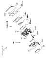
図1(A)、(B)はカメラモジュールが組み込まれた電子機器である携帯電話機10の一例を示す外観図である。
図1に示すように携帯電話機10は、ヒンジ部12によって揺動可能に連結された第1、第2の筐体14、16を有している。
第1の筐体14の内面には液晶表示パネル1402が設けられ、第2の筐体16の内面にはテンキーや機能キーなどの操作スイッチ1602が設けられている。
カメラモジュール20は、第1の筐体14の基端部に組み込まれ、カメラモジュール20で撮像した画像は液晶表示パネル1402に表示されるように構成されている。
(First embodiment)
Next, a first embodiment of the present invention will be described with reference to the drawings.
1A and 1B are external views illustrating an example of a
As shown in FIG. 1, the
A liquid
The
図2、図3はカメラモジュール20の分解斜視図、図4はカメラモジュール20の断面図である。
図2乃至図4に示すように、カメラモジュール20は、鏡筒22、撮像装置24、基板26などを含んで構成されている。
鏡筒22は、撮影光学系23を保持するものであり、撮影光学系23の光軸に沿った両側箇所に前端と後端とを有し、撮影光学系23を構成し最も前方に位置する光学部材28(本実施の形態ではレンズカバー)が鏡筒22の前端に露出して配置されている。
鏡筒22は矩形板状を呈し、鏡筒22の中央には前後方向に貫通する、言い換えると、前記撮影光学系23の光軸に沿って延在する収容空間が設けられている。
鏡筒22は、シャッタ支持用ハウジング30と、前鏡筒32と、後鏡筒34とが前記撮影光学系23の光軸方向に沿って重ね合わされて構成されている。
シャッタ支持用ハウジング30の中央には、前記撮影光学系23の光路の開口を開閉する不図示のシャッタおよびシャッタの駆動手段が設けられ、シャッタ支持用ハウジング30は、前鏡筒32のボス3202に対してねじ3002により結合されている。
図中、符号3004は、上述のシャッタの駆動手段を制御するためのフレキシブル基板を示している。
2 and 3 are exploded perspective views of the
As shown in FIGS. 2 to 4, the
The
The
The
In the center of the
In the figure,
撮像装置24は、撮影光学系23で結像された被写体像を撮像して撮像信号を出力するものであり、図2、図3に示すように、基板26上に設けられ、基板26とともに後鏡筒34の後端に取着されて配設される。
基板26は、撮像装置23から出力される撮像信号を入力して所定の信号処理を行なう信号処理部を有している。
The
The
図5(A)は撮像装置24の平面図、(B)は(A)のBB線断面図、(C)は(A)のCC線断面図、(D)は(A)のD矢視図である。
撮像装置24は、配線基板36と、枠体38と、撮像素子40と、透明カバー42とを含んで構成され、配線基板36の上に枠体38が配置され、配線基板36の上で枠体38の内側に撮像素子40が配置され、枠体38上に透明カバー42が配置されている。
5A is a plan view of the
The
撮像素子40は、撮影光学系23で結像された被写体像を撮像して撮像信号を生成するものであり、CCDやCMOSセンサ、あるいは公知のセンサを用いることができる。
撮像素子40は、矩形板状を呈し、その厚さ方向の一方に上面が、他方に下面が位置し、上面の中央には上面の輪郭よりも小さい寸法の矩形状の撮像面が形成され、撮像面を囲む矩形枠状の上面には撮像信号などを取り出すための配線用の複数の電極が形成されている。
The
The
配線基板36は、撮像素子40の下面の輪郭よりも大きな面積を有し、その上面に撮像素子40の下面が重ね合わされて熱硬化型接着剤2により接着されている。
配線基板36の上面には、導電材料からなる複数の電極(不図示)と、それら電極に接続された配線パターン(不図示)とが形成されている。
また、図5(D)に示すように配線基板36の下面には、前記配線パターンに接続され、基板26に半田付けで接続される複数の半田付けランド3604が形成されている。
配線基板36としては、ポリイミドをベースとしたフレキシブル配線基板や、ガラスクロスを用いた薄型有機基板を用いることができる。
図5(A)、(B)、(C)に示すように、撮像素子40の電極と配線基板36の電極とは、ワイヤー4がボンディングされることによって電気的に接続されている。
また、撮像素子40の下面に臨む配線基板36の箇所には1つまたは複数の貫通孔3602が形成されている。
なお、配線基板36の上面に設けられた複数の電極に対向する下面に銅パターンなどの硬い層を設けると、後述する前記電極に対するワイヤーボンディング性の向上を図る上で有利となる。
The
A plurality of electrodes (not shown) made of a conductive material and a wiring pattern (not shown) connected to the electrodes are formed on the upper surface of the
Further, as shown in FIG. 5D, a plurality of
As the
As shown in FIGS. 5A, 5 </ b> B, and 5 </ b> C, the electrode of the
In addition, one or a plurality of through
It should be noted that providing a hard layer such as a copper pattern on the lower surface facing the plurality of electrodes provided on the upper surface of the
枠体38は、撮像素子40をその内側に収容できるように撮像素子40よりも大きい輪郭の収容空間Sを有する矩形枠状を呈し、本実施の形態では、配線基板36と枠体38とが同一の輪郭で形成されている。
枠体38の厚さ方向の一方に上面が、他方に下面が位置し、撮像素子40の外側を覆うように枠体38の下面が配線基板36の上面に重ね合わされて熱硬化型接着剤2により接着されている。
なお、熱硬化型接着剤2は、貫通孔3602と収容空間Sとが連通するような形状と量で設けられている。
また、本実施の形態では、図5(D)に示すように、配線基板36の半田付けランド部3604が、撮像素子40および枠体38が取着される面とは反対側に位置する配線基板36の面に設けられ、半田付け用ランド部3604は枠体38の輪郭3610の範囲に配置されている。
枠体38は、配線基板36よりも小さい熱膨張率を有し、かつ、配線基板36よりも大きい剛性を有する材料で形成されている。
例えば、枠体38の線膨張係数は、配線基板36の線膨張係数の1/2以下である。
枠体38の剛性は、枠体38と配線基板36とが熱硬化型接着剤2で結合された状態で、配線基板36に反りやねじれが生じようとしても枠体38が抵抗し、それら反りやねじれといった変形を阻止する程度の差を配線基板36との間に有している。
枠体38の材料としては、例えば、セラミック、あるいは、金属を用いることができ、金属としては42−alloy、コバールなどを採用可能である。
The
The upper surface is located on one side in the thickness direction of the
The
Further, in the present embodiment, as shown in FIG. 5D, the wiring in which the
The
For example, the linear expansion coefficient of the
The rigidity of the
As a material of the
配線基板36および枠体38の具体例として、例えば、次のものを例示することができる。
配線基板36は、線膨張係数32×10−6、弾性率3.2GPaのフレキシブル配線基板とし、枠体38は、線膨張係数7.2×10⁻⁶、弾性率270GPaのセラミック材料とすることができる。
As specific examples of the
The
透明カバー42は、収容空間Sを閉塞可能な大きさの矩形板状に形成され、枠体38の上面に重ね合わされて熱硬化型接着剤2により接着され、これにより収容空間S内の撮像素子40が封止されている。
透明カバー42の材料としては、撮像素子40の撮像面に対して光を透過可能なものであればよく、透明なガラスや合成樹脂を用いることができる。
The
The material of the
次に、製造方法について2つの例を挙げて説明する。
図6は撮像装置24の第1の製造工程を示す説明図である。
図6(A)に示すように、まず、配線基板36の上面で、撮像素子40と枠体38に対応する箇所に熱硬化型接着剤2を塗布する(樹脂塗布)。
次に、図6(B)に示すように、撮像素子40を配線基板36の上面に位置決めして載置する(ダイボンディング)。
次に、図6(C)に示すように、枠体38を配線基板36の上面に位置決めして載置する(枠搭載)。
次に、図6(D)に示すように、加熱室H(あるいは加熱炉やオーブンなど)(図7参照)において、配線基板36の上面に撮像素子40と枠体38が載置された状態で加熱を行い熱硬化型接着剤2を熱硬化させ、配線基板36の上面に撮像素子40と枠体38を接着固定する(樹脂硬化)。
次に、図6(E)に示すように、加熱室Hから取り出し、配線基板36の上面の電極と撮像素子40の上面の電極との間をワイヤー4を用いて電気的に接続する(ワイヤーボンディング)。
次に、図6(F)に示すように、枠体38の上面に熱硬化型接着剤2を塗布する(樹脂塗布)。
次に、図6(G)に示すように、枠体38の上面に透明カバー42を載置する(透明蓋体搭載)。
次に、図6(H)に示すように、加熱室Hにおいて、枠体38の上面に透明カバー42が載置された状態で加熱を行い熱硬化型接着剤2を熱硬化させ、枠体38と透明カバー42を接着固定する(樹脂硬化)。
次に、加熱室Hから取り出し、図6(I)に示すように撮像装置24が完成する(完成)。
Next, the manufacturing method will be described with two examples.
FIG. 6 is an explanatory diagram showing a first manufacturing process of the
As shown in FIG. 6A, first, the
Next, as shown in FIG. 6B, the
Next, as shown in FIG. 6C, the
Next, as shown in FIG. 6D, the
Next, as shown in FIG. 6 (E), it is taken out from the heating chamber H and electrically connected between the electrode on the upper surface of the
Next, as shown in FIG. 6F, the
Next, as shown in FIG. 6G, the
Next, as shown in FIG. 6 (H), in the heating chamber H, heating is performed with the
Next, it is taken out from the heating chamber H, and the
次に、図7を参照して本実施の形態の作用効果について説明する。
図7は配線基板36に枠体38および撮像素子40が熱硬化型接着剤2によって接着固定される際の原理を説明する図であり、図6(D)の樹脂硬化の工程とその前後の状態を示している。
図7(A)に示すように、加熱硬化前の状態では配線基板36の上面に枠体38および撮像素子40が熱硬化型接着剤2を介して載置されている。
図7(B−1)に示すように、加熱の前半においては、熱硬化型接着剤2が未だ十分に加熱されていないため、未硬化である。
一方、前記加熱によって、配線基板36および枠体38の双方がそれぞれの熱膨張率に比例して膨張するが、枠体38は、配線基板36よりも小さい熱膨張率を有していることから、配線基板36の膨張は枠体38の膨張よりも大きなものとなっている。
図7(B−2)に示すように、加熱の後半においては、配線基板36および枠体38が膨張した状態のままで熱硬化型接着剤2が加熱硬化され、配線基板36の上面に枠体38および撮像素子40が固定される。
そして、図7(C)に示すように、加熱硬化後、温度が下がると、配線基板36および枠体38の双方がそれぞれの熱膨張率に比例して収縮しようとするが、枠体38は、配線基板36よりも小さい熱膨張率を有し、かつ、枠体38は配線基板36よりも大きい剛性を有していることから、配線基板36はその熱膨張率に比例して収縮できず、配線基板36の周囲が熱硬化型接着剤2を介して枠体38に引っ張られ、配線基板36には引っ張り応力が作用している状態となる。
したがって、この引っ張り応力によって配線基板36に反りやねじれが生じようとしても枠体38が抵抗し、それら反りやねじれといった変形が阻止され、配線基板36は平坦な状態に維持される。
したがって、本実施の形態によれば、撮像装置24の配線基板36として厚さが薄く剛性の低い材料を用いたとしても、配線基板36に反りやねじれが生じず、配線基板36の平坦性が得られる。
そのため、撮像素子40のあおり低減、ワイヤーボンディング性の向上の確保、配線基板36と基板26とのはんだ接合性の向上を図る上で有利となり、撮像装置24の信頼性の向上、小型化、薄型化、軽量化を図る上で有利となる。
Next, the effect of this Embodiment is demonstrated with reference to FIG.
FIG. 7 is a diagram for explaining the principle when the
As shown in FIG. 7A, the
As shown in FIG. 7 (B-1), in the first half of heating, the
On the other hand, both the
As shown in FIG. 7B-2, in the second half of heating, the
Then, as shown in FIG. 7C, when the temperature decreases after heat curing, both the
Therefore, even if the
Therefore, according to the present embodiment, even if a thin and low-rigidity material is used for the
Therefore, it is advantageous in reducing the tilt of the
また、本実施の形態では、配線基板36に枠体38と撮像素子40とを接着する際に熱硬化型接着剤2を用いたので、一回の加熱によって配線基板36に枠体38と撮像素子40を同時に結合でき、キュア工程を共通化することが可能となるので、タクト低減・工数削減が可能となる。
また、本実施の形態では、配線基板36に貫通孔3602を設けることで、撮像素子40を配置している収容空間Sと枠体38の外部とが連通されているので、収容空間Sと、枠体38の外部との環境に差が発生せず、高い信頼性を得る上で有利となる。なお、収容空間Sと枠体38の外部とを連通する貫通孔を枠体38に設けた場合には枠体38の剛性低下を招くが、本実施の形態では、枠体38に貫通孔を設ける必要がないので枠体38の剛性を確保する上で有利となる。
また、配線基板36に貫通孔3602を設けることで、熱硬化型接着剤2の加熱硬化時に内圧の上昇を抑えることが出来るため、透明カバー42を枠体38に接着固定する工程において、熱硬化型接着剤2を使用する上で有利となる。
また、本実施の形態では、配線基板36の半田付けランド部3604が、配線基板36の下面において枠体38の輪郭3810の範囲に配置されており、言い換えると、配線基板36の半田付けランド部3604を枠体38の下面に集中して配置されているので、半田付けランド部3604は枠体38に倣うため平面度の確保が容易となり、安定した半田付けを行うことができ半田付け性の向上を図る上で有利となる。
また、半田付けランド部3604は平坦性とともに高剛性を得ているため、接触・非接触を問わず電気チェッカーでの検査を行なう上で有利となる。
Further, in the present embodiment, since the
Further, in the present embodiment, by providing the through
Further, by providing the through-
In the present embodiment, the soldering
Further, since the
次に、撮像装置24の第2の製造工程について説明する。
図8は撮像装置24の第2の製造工程を示す説明図である。
図8(A)に示すように、まず、配線基板36の上面で、撮像素子40に対応する箇所に熱硬化型接着剤2を塗布する(樹脂塗布)。
次に、図8(B)に示すように、撮像素子40を配線基板36の上面に位置決めして載置する(ダイボンディング)。
次に、図8(C)に示すように、加熱室H(図7参照)において、配線基板36の上面に撮像素子40が載置された状態で加熱を行い熱硬化型接着剤2を熱硬化させ、配線基板36の上面に撮像素子40を接着固定する(樹脂硬化)。
次に、図8(D)に示すように、加熱室Hから取り出し、配線基板36の上面の電極と撮像素子40の上面の電極との間をワイヤー4を用いて電気的に接続する(ワイヤーボンディング)。
次に、図8(E)に示すように、まず、配線基板36の上面で、枠体38に対応する箇所に熱硬化型接着剤2を塗布する(樹脂塗布)。
次に、図8(F)に示すように、枠体38を配線基板36の上面に位置決めして載置する(枠搭載)。
次に、図8(G)に示すように、枠体38の上面に熱硬化型接着剤2を塗布する(樹脂塗布)。
次に、図8(H)に示すように、枠体38の上面に透明カバー42を載置する(透明蓋体搭載)。
次に、図8(I)に示すように、加熱室Hにおいて、配線基板36の上面に枠体38が載置され、かつ、枠体38の上面に透明カバー42が載置された状態で加熱を行い熱硬化型接着剤2を熱硬化させ、配線基板36の上面に枠体38を接着固定するとともに、枠体38に透明カバー42を接着固定する(樹脂硬化)。
次に、加熱室Hから取り出し、図8(J)に示すように撮像装置24が完成する(完成)。
Next, a second manufacturing process of the
FIG. 8 is an explanatory diagram showing a second manufacturing process of the
As shown in FIG. 8A, first, the
Next, as shown in FIG. 8B, the
Next, as shown in FIG. 8C, in the heating chamber H (see FIG. 7), heating is performed with the
Next, as shown in FIG. 8D, the electrode is taken out from the heating chamber H and electrically connected between the electrode on the upper surface of the
Next, as shown in FIG. 8 (E), first, the
Next, as shown in FIG. 8F, the
Next, as shown in FIG. 8G, the
Next, as shown in FIG. 8H, the
Next, as shown in FIG. 8I, in the heating chamber H, the
Next, it is taken out from the heating chamber H, and the
このような第2の製造工程によって製作された撮像装置24においても第1の製造工程によって製作された撮像装置24と同様の効果が奏される。
なお、第1の製造工程では、枠体38が配線基板36に接着固定された後で、枠体38の内側でワイヤーボンディングを行なうため、撮像素子40と枠体38の間のスペースを確保する必要がある。
これに対して、第2の製造工程では、ワイヤーボンディング(図8(D))の後に枠体38を配線基板36に接着固定(図8(I))しているため、撮像素子40と枠体38の間のスペースを第1の製造工程よりも縮小でき、言い換えると、ワイヤーボンディングの2ndボンディング点(撮像素子40の電極)と枠体38の内壁間の距離を低減することが可能であり、これにより枠体38の小型化、ひいては、撮像装置24の小型化を図る上で有利となる。
また、第2の製造工程では、透明カバー42を枠体38に接着固定する接着剤として、配線基板36に枠体38を接着固定する熱硬化型接着剤2と同一のものを用いたので、図8(I)において、それらの熱硬化型接着剤2を一度に硬化でき、したがって、枠体38や透明カバー42に加わる応力を緩和することが可能であり、信頼性を確保する上で有利となる。
The
In the first manufacturing process, after the
On the other hand, in the second manufacturing process, the
In the second manufacturing process, the same adhesive as the
なお、本実施の形態では、配線基板36と枠体38とが同一の輪郭である場合について説明したが、配線基板36の形状は枠体38よりも大きいものであってよく、その場合には、枠体38が取着された範囲内において配線基板36の平面性を確保することが可能となる。
また、本実施の形態では、配線基板36に半田付けランド部3604を設け、この半田付けランド部3604を基板24に半田付けすることで、撮像装置24の撮像素子40で生成される撮像信号などを基板26に供給する場合について説明したが、本発明はこれに限定されるものではない。例えば、半田付けランド部3604を設ける代わりに、配線基板36から帯状に延出する引き出し部を設けるとともに、この引き出し部に接続コネクタを設け、この接続コネクタを介して配線基板36から基板26に撮像信号などを供給するようにしてもよい。
また、実施の形態では、電子機器が携帯電話機10である場合について説明したが、本発明は、例えば、PDA、ノート型パーソナルコンピュータなどの携帯情報端末、あるいは、デジタルスチルカメラ、ビデオカメラなどの種々のカメラ装置に広く適用可能である。
In the present embodiment, the case where the
Further, in the present embodiment, the soldering
In the embodiment, the case where the electronic device is the
2……熱硬化型接着剤、10……携帯電話機、20……カメラモジュール、24……撮
像装置、36……配線基板、38……枠体、40……撮像素子、42……透明カバー。
2 ... Thermosetting adhesive, 10 ... Mobile phone, 20 ... Camera module, 24 ... Imaging device, 36 ... Wiring board, 38 ... Frame, 40 ... Imaging device, 42 ... Transparent cover .
Claims (11)
前記配線基板の一方の面に配置された枠体と、
前記配線基板の前記一方の面で前記枠体の内側に配置された撮像素子と、
前記枠体上に配置された透明カバーとを備え、
前記配線基板と前記枠体は熱硬化型接着剤により取着され、
前記配線基板に貫通孔を設けている
ことを特徴とする撮像装置。 A wiring board;
A frame disposed on one surface of the wiring board;
An image sensor disposed inside the frame on the one surface of the wiring board;
A transparent cover disposed on the frame,
The wiring board and the frame are attached by a thermosetting adhesive,
A through-hole is provided in the wiring board.
ことを特徴とする請求項1記載の撮像装置。 The imaging device according to claim 1, wherein the through hole is formed in a portion of the wiring board that faces a lower surface of the imaging element.
ことを特徴とする請求項1記載の撮像装置。 The imaging apparatus according to claim 1, wherein the wiring board, the imaging element, the frame, and the transparent cover are each attached by a thermosetting adhesive.
前記貫通孔と前記枠体の内側に有する空間とが連通するように前記配線基板と前記撮像素子を取着するための前記熱硬化型接着剤が設けられている
ことを特徴とする請求項3記載の撮像装置。 The through hole is formed in a portion facing the lower surface of the imaging element in the wiring board,
The thermosetting adhesive for attaching the wiring board and the imaging element is provided so that the through hole and a space inside the frame communicate with each other. The imaging device described.
ことを特徴とする請求項1記載の撮像装置。 A soldering land portion is provided on the other surface of the wiring board, and the soldering land portion is disposed in a range in which the outline of the frame is projected in a direction perpendicular to the other surface. The imaging device according to claim 1.
ことを特徴とする請求項1記載の撮像装置。 The imaging device according to claim 1, wherein the imaging element and the wiring board are electrically connected by a wire.
前記撮像装置は、配線基板と、前記配線基板の一方の面に配置された枠体と、前記配線基板の前記一方の面で前記枠体の内側に配置された撮像素子と、前記枠体上に配置された透明カバーとを備え、
前記配線基板と前記枠体は熱硬化型接着剤により取着され、
前記配線基板に貫通孔を設けている
ことを特徴とするカメラモジュール。 An imaging device that captures an image of a subject that is incorporated in the lens barrel and imaged by the imaging optical system, and that outputs an imaging signal, a lens barrel that holds the imaging optical system, a substrate attached to the lens barrel, and And a signal processing unit that is provided on the substrate and receives an imaging signal output from the imaging device and performs predetermined signal processing,
The imaging device includes a wiring board, a frame disposed on one surface of the wiring board, an imaging element disposed on the inner side of the frame on the one surface of the wiring board, and the frame And a transparent cover arranged on the
The wiring board and the frame are attached by a thermosetting adhesive,
A camera module, wherein a through hole is provided in the wiring board.
前記カメラモジュールは、撮影光学系を保持する鏡筒と、前記鏡筒に取着された基板と、前記鏡筒内に組み込まれ前記撮影光学系で結像された被写体像を撮像して撮像信号を出力する撮像装置と、前記基板に設けられ前記撮像装置から出力される撮像信号を入力して所定の信号処理を行なう信号処理部とを含んで構成され、
前記撮像装置は、配線基板と、前記配線基板の一方の面に配置された枠体と、前記配線基板の前記一方の面で前記枠体の内側に配置された撮像素子と、前記枠体上に配置された透明カバーとを備え、
前記配線基板と前記枠体は熱硬化型接着剤により取着され、
前記配線基板に貫通孔を設けている
ことを特徴とする電子機器。 An electronic device comprising a housing and a camera module incorporated in the housing,
The camera module captures an image signal obtained by imaging a lens barrel that holds a photographic optical system, a substrate attached to the lens barrel, and a subject image that is incorporated in the lens barrel and imaged by the photographic optical system. And a signal processing unit that is provided on the substrate and receives an imaging signal output from the imaging device and performs predetermined signal processing,
The imaging device includes a wiring board, a frame disposed on one surface of the wiring board, an imaging element disposed on the inner side of the frame on the one surface of the wiring board, and the frame And a transparent cover arranged on the
The wiring board and the frame are attached by a thermosetting adhesive,
An electronic device, wherein a through hole is provided in the wiring board.
前記配線基板の一方の面に配置された枠体と、
前記配線基板の前記一方の面で前記枠体の内側に配置された撮像素子と、
前記枠体上に配置された透明カバーとを備え、
前記配線基板と前記枠体は熱硬化型接着剤により取着された撮像装置の製造方法であって、
前記配線基板上に前記熱硬化型接着剤を介在させて前記枠体を載置し、この状態で加熱し前記熱硬化型接着剤を硬化させ、
前記貫通孔によって前記枠体内側の内圧の上昇を抑えるようにした
ことを特徴とする撮像装置の製造方法。 A wiring board provided with a through hole;
A frame disposed on one surface of the wiring board;
An image sensor disposed inside the frame on the one surface of the wiring board;
A transparent cover disposed on the frame,
The wiring board and the frame are manufacturing methods of an imaging device attached with a thermosetting adhesive,
The frame body is placed on the wiring board with the thermosetting adhesive interposed therebetween, heated in this state to cure the thermosetting adhesive,
An increase in internal pressure inside the frame body is suppressed by the through-hole.
ことを特徴とする請求項9記載の撮像装置の製造方法。 When the frame is attached on the wiring board by curing the thermosetting adhesive, the imaging element is attached on the wiring board with the thermosetting adhesive, and then the imaging element is attached. And the electrode on the wiring board are connected by wire bonding, and then the transparent cover is placed on the frame with a thermosetting adhesive interposed therebetween, and the thermosetting adhesive is heated in this state. The method of manufacturing an imaging apparatus according to claim 9, wherein the transparent cover is attached to the frame body by curing.
ことを特徴とする請求項9記載の撮像装置の製造方法。 Before attaching the frame body on the wiring board by curing the thermosetting adhesive, the imaging element is attached on the wiring board with a thermosetting adhesive, and then the imaging element and the The electrode on the wiring board is connected by wire bonding, and then the frame body is attached. At the same time, the transparent cover is placed on the frame body with a thermosetting adhesive interposed therebetween, and heated. The method of manufacturing an imaging apparatus according to claim 9, wherein the thermosetting adhesive is cured to attach the transparent cover to the frame.
Priority Applications (1)
| Application Number | Priority Date | Filing Date | Title |
|---|---|---|---|
| JP2010115470A JP2010220245A (en) | 2010-05-19 | 2010-05-19 | Imaging device, camera module, electronic device, and method of manufacturing imaging device |
Applications Claiming Priority (1)
| Application Number | Priority Date | Filing Date | Title |
|---|---|---|---|
| JP2010115470A JP2010220245A (en) | 2010-05-19 | 2010-05-19 | Imaging device, camera module, electronic device, and method of manufacturing imaging device |
Related Parent Applications (1)
| Application Number | Title | Priority Date | Filing Date |
|---|---|---|---|
| JP2006025779A Division JP2007208045A (en) | 2006-02-02 | 2006-02-02 | Imaging device, camera module, electronic device, and manufacturing method of imaging device |
Publications (1)
| Publication Number | Publication Date |
|---|---|
| JP2010220245A true JP2010220245A (en) | 2010-09-30 |
Family
ID=42978499
Family Applications (1)
| Application Number | Title | Priority Date | Filing Date |
|---|---|---|---|
| JP2010115470A Pending JP2010220245A (en) | 2010-05-19 | 2010-05-19 | Imaging device, camera module, electronic device, and method of manufacturing imaging device |
Country Status (1)
| Country | Link |
|---|---|
| JP (1) | JP2010220245A (en) |
Cited By (3)
| Publication number | Priority date | Publication date | Assignee | Title |
|---|---|---|---|---|
| JP2018088555A (en) * | 2012-04-27 | 2018-06-07 | キヤノン株式会社 | Electronic component and electronic module, and method of manufacturing the same |
| US10720394B2 (en) | 2015-11-19 | 2020-07-21 | Kyocera Corporation | Electronic component mounting board and electronic device |
| US11483935B2 (en) | 2020-02-10 | 2022-10-25 | Samsung Electronics Co., Ltd. | PCB structure and electronic device including the same |
Citations (3)
| Publication number | Priority date | Publication date | Assignee | Title |
|---|---|---|---|---|
| JP2004327531A (en) * | 2003-04-22 | 2004-11-18 | Mitsubishi Electric Corp | Imaging apparatus |
| JP2005026426A (en) * | 2003-07-01 | 2005-01-27 | Matsushita Electric Ind Co Ltd | Solid-state imaging device and manufacturing method thereof |
| JP2005286028A (en) * | 2004-03-29 | 2005-10-13 | Sharp Corp | Solid-state imaging device package, manufacturing method thereof semiconductor package, and camera module |
-
2010
- 2010-05-19 JP JP2010115470A patent/JP2010220245A/en active Pending
Patent Citations (3)
| Publication number | Priority date | Publication date | Assignee | Title |
|---|---|---|---|---|
| JP2004327531A (en) * | 2003-04-22 | 2004-11-18 | Mitsubishi Electric Corp | Imaging apparatus |
| JP2005026426A (en) * | 2003-07-01 | 2005-01-27 | Matsushita Electric Ind Co Ltd | Solid-state imaging device and manufacturing method thereof |
| JP2005286028A (en) * | 2004-03-29 | 2005-10-13 | Sharp Corp | Solid-state imaging device package, manufacturing method thereof semiconductor package, and camera module |
Cited By (3)
| Publication number | Priority date | Publication date | Assignee | Title |
|---|---|---|---|---|
| JP2018088555A (en) * | 2012-04-27 | 2018-06-07 | キヤノン株式会社 | Electronic component and electronic module, and method of manufacturing the same |
| US10720394B2 (en) | 2015-11-19 | 2020-07-21 | Kyocera Corporation | Electronic component mounting board and electronic device |
| US11483935B2 (en) | 2020-02-10 | 2022-10-25 | Samsung Electronics Co., Ltd. | PCB structure and electronic device including the same |
Similar Documents
| Publication | Publication Date | Title |
|---|---|---|
| JP2007208045A (en) | Imaging device, camera module, electronic device, and manufacturing method of imaging device | |
| CN108322632B (en) | Camera module, electronic device and camera module manufacturing method | |
| JP3607160B2 (en) | Imaging device | |
| JP4276678B2 (en) | Imaging device | |
| CN101170105A (en) | Optical device module and its manufacturing method, and optical device unit and its manufacturing method | |
| JP5117967B2 (en) | Electronic equipment and electronic equipment with imaging function | |
| JP2007274624A (en) | Camera module | |
| CN109981842A (en) | Display module, electronic device and manufacturing method of display module | |
| JP2013005047A (en) | Image pickup device and electronic apparatus using the same | |
| JP2011101228A (en) | Ceramic package and camera module | |
| JP2010263020A (en) | Optical device module | |
| TW201008259A (en) | Assembly for image sensing chip and assembling method thereof | |
| JPWO2007096992A1 (en) | Imaging device and portable terminal device | |
| CN103081105B (en) | Image pick-up device, image pickup model and camera | |
| JP2008148253A (en) | Camera module, and imaging apparatus and assembling method thereof | |
| JP2010220245A (en) | Imaging device, camera module, electronic device, and method of manufacturing imaging device | |
| KR101661660B1 (en) | Camera module | |
| JP2005295050A (en) | Camera module | |
| KR20220068970A (en) | Camera module | |
| JP3839019B2 (en) | Imaging device | |
| JP2015088498A (en) | Solid image pickup device and electronic camera | |
| KR20060104962A (en) | Device for camera module | |
| JP6149502B2 (en) | Imaging unit and imaging apparatus | |
| JP3821831B2 (en) | Imaging device | |
| KR100966967B1 (en) | Camera module and manufacturing method |
Legal Events
| Date | Code | Title | Description |
|---|---|---|---|
| A977 | Report on retrieval |
Free format text: JAPANESE INTERMEDIATE CODE: A971007 Effective date: 20120113 |
|
| A131 | Notification of reasons for refusal |
Free format text: JAPANESE INTERMEDIATE CODE: A131 Effective date: 20120117 |
|
| A521 | Request for written amendment filed |
Free format text: JAPANESE INTERMEDIATE CODE: A523 Effective date: 20120305 |
|
| A131 | Notification of reasons for refusal |
Free format text: JAPANESE INTERMEDIATE CODE: A131 Effective date: 20120710 |
|
| A02 | Decision of refusal |
Free format text: JAPANESE INTERMEDIATE CODE: A02 Effective date: 20121106 |