JP2009295556A - Discharge lamp device - Google Patents
Discharge lamp device Download PDFInfo
- Publication number
- JP2009295556A JP2009295556A JP2008150954A JP2008150954A JP2009295556A JP 2009295556 A JP2009295556 A JP 2009295556A JP 2008150954 A JP2008150954 A JP 2008150954A JP 2008150954 A JP2008150954 A JP 2008150954A JP 2009295556 A JP2009295556 A JP 2009295556A
- Authority
- JP
- Japan
- Prior art keywords
- circuit
- current
- detection circuit
- transformer
- voltage
- Prior art date
- Legal status (The legal status is an assumption and is not a legal conclusion. Google has not performed a legal analysis and makes no representation as to the accuracy of the status listed.)
- Pending
Links
- 238000001514 detection method Methods 0.000 claims abstract description 120
- 238000012935 Averaging Methods 0.000 claims abstract description 59
- 238000006243 chemical reaction Methods 0.000 claims abstract description 31
- 239000007789 gas Substances 0.000 description 61
- 238000010586 diagram Methods 0.000 description 22
- 239000011521 glass Substances 0.000 description 13
- 239000003990 capacitor Substances 0.000 description 12
- 229910052756 noble gas Inorganic materials 0.000 description 8
- 230000003252 repetitive effect Effects 0.000 description 6
- QSHDDOUJBYECFT-UHFFFAOYSA-N mercury Chemical compound [Hg] QSHDDOUJBYECFT-UHFFFAOYSA-N 0.000 description 5
- 229910052753 mercury Inorganic materials 0.000 description 5
- 238000000034 method Methods 0.000 description 5
- 239000000463 material Substances 0.000 description 4
- 238000007789 sealing Methods 0.000 description 4
- 229910052743 krypton Inorganic materials 0.000 description 3
- XKRFYHLGVUSROY-UHFFFAOYSA-N Argon Chemical compound [Ar] XKRFYHLGVUSROY-UHFFFAOYSA-N 0.000 description 2
- 229910052782 aluminium Inorganic materials 0.000 description 2
- XAGFODPZIPBFFR-UHFFFAOYSA-N aluminium Chemical compound [Al] XAGFODPZIPBFFR-UHFFFAOYSA-N 0.000 description 2
- 229910052786 argon Inorganic materials 0.000 description 2
- 239000000460 chlorine Substances 0.000 description 2
- 239000004020 conductor Substances 0.000 description 2
- 238000005286 illumination Methods 0.000 description 2
- 238000003780 insertion Methods 0.000 description 2
- 230000037431 insertion Effects 0.000 description 2
- DNNSSWSSYDEUBZ-UHFFFAOYSA-N krypton atom Chemical compound [Kr] DNNSSWSSYDEUBZ-UHFFFAOYSA-N 0.000 description 2
- 239000004973 liquid crystal related substance Substances 0.000 description 2
- 230000003071 parasitic effect Effects 0.000 description 2
- 229910052724 xenon Inorganic materials 0.000 description 2
- ZAMOUSCENKQFHK-UHFFFAOYSA-N Chlorine atom Chemical compound [Cl] ZAMOUSCENKQFHK-UHFFFAOYSA-N 0.000 description 1
- OAICVXFJPJFONN-UHFFFAOYSA-N Phosphorus Chemical compound [P] OAICVXFJPJFONN-UHFFFAOYSA-N 0.000 description 1
- VYPSYNLAJGMNEJ-UHFFFAOYSA-N Silicium dioxide Chemical compound O=[Si]=O VYPSYNLAJGMNEJ-UHFFFAOYSA-N 0.000 description 1
- 230000002159 abnormal effect Effects 0.000 description 1
- 230000004888 barrier function Effects 0.000 description 1
- 229910052801 chlorine Inorganic materials 0.000 description 1
- 230000000694 effects Effects 0.000 description 1
- 238000003912 environmental pollution Methods 0.000 description 1
- 238000000605 extraction Methods 0.000 description 1
- 229910052736 halogen Inorganic materials 0.000 description 1
- 150000002367 halogens Chemical class 0.000 description 1
- 229910052734 helium Inorganic materials 0.000 description 1
- 238000009413 insulation Methods 0.000 description 1
- 229910052751 metal Inorganic materials 0.000 description 1
- 239000002184 metal Substances 0.000 description 1
- 230000010355 oscillation Effects 0.000 description 1
- 230000005855 radiation Effects 0.000 description 1
- 229910052761 rare earth metal Inorganic materials 0.000 description 1
- 150000002910 rare earth metals Chemical class 0.000 description 1
- 238000007650 screen-printing Methods 0.000 description 1
- 239000005394 sealing glass Substances 0.000 description 1
- FHNFHKCVQCLJFQ-UHFFFAOYSA-N xenon atom Chemical compound [Xe] FHNFHKCVQCLJFQ-UHFFFAOYSA-N 0.000 description 1
Images


Classifications
-
- H—ELECTRICITY
- H05—ELECTRIC TECHNIQUES NOT OTHERWISE PROVIDED FOR
- H05B—ELECTRIC HEATING; ELECTRIC LIGHT SOURCES NOT OTHERWISE PROVIDED FOR; CIRCUIT ARRANGEMENTS FOR ELECTRIC LIGHT SOURCES, IN GENERAL
- H05B41/00—Circuit arrangements or apparatus for igniting or operating discharge lamps
- H05B41/14—Circuit arrangements
- H05B41/24—Circuit arrangements in which the lamp is fed by high frequency AC, or with separate oscillator frequency
-
- H—ELECTRICITY
- H05—ELECTRIC TECHNIQUES NOT OTHERWISE PROVIDED FOR
- H05B—ELECTRIC HEATING; ELECTRIC LIGHT SOURCES NOT OTHERWISE PROVIDED FOR; CIRCUIT ARRANGEMENTS FOR ELECTRIC LIGHT SOURCES, IN GENERAL
- H05B41/00—Circuit arrangements or apparatus for igniting or operating discharge lamps
- H05B41/14—Circuit arrangements
- H05B41/26—Circuit arrangements in which the lamp is fed by power derived from DC by means of a converter, e.g. by high-voltage DC
- H05B41/28—Circuit arrangements in which the lamp is fed by power derived from DC by means of a converter, e.g. by high-voltage DC using static converters
- H05B41/282—Circuit arrangements in which the lamp is fed by power derived from DC by means of a converter, e.g. by high-voltage DC using static converters with semiconductor devices
- H05B41/285—Arrangements for protecting lamps or circuits against abnormal operating conditions
-
- Y—GENERAL TAGGING OF NEW TECHNOLOGICAL DEVELOPMENTS; GENERAL TAGGING OF CROSS-SECTIONAL TECHNOLOGIES SPANNING OVER SEVERAL SECTIONS OF THE IPC; TECHNICAL SUBJECTS COVERED BY FORMER USPC CROSS-REFERENCE ART COLLECTIONS [XRACs] AND DIGESTS
- Y02—TECHNOLOGIES OR APPLICATIONS FOR MITIGATION OR ADAPTATION AGAINST CLIMATE CHANGE
- Y02B—CLIMATE CHANGE MITIGATION TECHNOLOGIES RELATED TO BUILDINGS, e.g. HOUSING, HOUSE APPLIANCES OR RELATED END-USER APPLICATIONS
- Y02B20/00—Energy efficient lighting technologies, e.g. halogen lamps or gas discharge lamps
Landscapes
- Circuit Arrangements For Discharge Lamps (AREA)
- Inverter Devices (AREA)
Abstract
【課題】希ガス蛍光ランプ等を使用した放電ランプ装置において、無負荷時と点灯時を確実に峻別し検知すること。
【解決手段】第1スイッチ素子と第2スイッチ素子を交互に動作させて交流電圧に出力する交流変換回路2と、前記交流電圧を昇圧するトランス3の2次側に希ガス蛍光ランプ4を備えた放電ランプ装置において、第1スイッチ素子のオン時に流れる第1電流経路と第2スイッチ素子のオン時に流れる第2電流経路とが重なると共に、第1電流経路と第2電流経路を流れる電流が互いに逆方向である電流経路に接続された電流波形検出回路51と、第1スイッチ素子のオン期間を含み第2スイッチ素子のオン期間を含まない略半周期間、電流波形検出回路の検出電流を通過させるスイッチ回路52と、スイッチ回路を通過した電流を平均化する平均化回路53と、平均化回路の出力値を基準値と比較する比較回路54とからなる無負荷検知回路5を設けたことを特徴とする。
【選択図】図1
In a discharge lamp device using a rare gas fluorescent lamp or the like, it is possible to reliably distinguish and detect when there is no load and when it is lit.
An AC conversion circuit 2 that alternately operates a first switch element and a second switch element to output an AC voltage, and a rare gas fluorescent lamp 4 on a secondary side of a transformer 3 that boosts the AC voltage. In the discharge lamp device described above, the first current path that flows when the first switch element is on and the second current path that flows when the second switch element are on overlap, and the currents that flow through the first current path and the second current path mutually The current waveform detection circuit 51 connected to the current path in the reverse direction and the detection current of the current waveform detection circuit are allowed to pass for approximately half a period including the ON period of the first switch element but not the ON period of the second switch element. A no-load detection circuit comprising a switch circuit 52, an averaging circuit 53 that averages the current that has passed through the switch circuit, and a comparison circuit 54 that compares the output value of the averaging circuit with a reference value. 5, characterized in that the provided.
[Selection] Figure 1
Description
本発明は、放電ランプ装置に係わり、特に、放電ランプとして希ガス蛍光ランプを用いた、液晶ディスプレイパネルのバックライト光源や照明用光源等に用いられる放電ランプ装置に関する。 The present invention relates to a discharge lamp device, and more particularly to a discharge lamp device that uses a rare gas fluorescent lamp as a discharge lamp and is used for a backlight light source, an illumination light source, and the like of a liquid crystal display panel.
従来、液晶ディスプレイパネルのバックライト光源や照明用光源として、冷陰極蛍光ランプや熱陰極蛍光ランプが多く用いられている。これらのランプは、内部に微量の水銀が封入されており、放電により励起された水銀から発生する紫外線により蛍光体を発光させるものであり、高輝度で、かつ効率的な発光が得られる点で優れている。 Conventionally, cold cathode fluorescent lamps and hot cathode fluorescent lamps are often used as backlight sources and illumination light sources of liquid crystal display panels. These lamps contain a very small amount of mercury inside, and emit phosphors by ultraviolet rays generated from mercury excited by discharge, so that high-luminance and efficient light emission can be obtained. Are better.
しかし、近年、環境汚染の防止の観点から、水銀を含まない新しい光源が望まれている。水銀を含まない蛍光ランプとしては、ガラス管の外面に帯状の複数本の電極を配設し、これらの電極に、例えば、トランスで昇圧された高周波の高電圧を印加して点灯する希ガス蛍光ランプが提案されている。 However, in recent years, a new light source that does not contain mercury is desired from the viewpoint of preventing environmental pollution. As a fluorescent lamp that does not contain mercury, a plurality of strip-shaped electrodes are arranged on the outer surface of a glass tube, and a high-frequency high voltage boosted by a transformer, for example, is applied to these electrodes to turn on the rare gas fluorescence. A lamp has been proposed.
ところで、希ガス蛍光ランプは、何等かの事情で配線が外れたり、発光管の破損でガスリークが生じ、点灯ができなくなるような、いわゆる無負荷状態になることも想定しておかなければならない。無負荷状態になると、回路中の寄生容量、寄生インダクタンスによる共振で高電圧が生じ、装置内の高周波電源が破損したり、装置内の回路の絶縁部を破壊するような異常事態が引き起こされるおそれがある。そのため、このような無負荷状態を迅速に検知して装置を停止させる等の処置が必要である。 By the way, it is necessary to assume that the rare gas fluorescent lamp is in a so-called no-load state in which the wiring is disconnected for some reason or the arc tube is broken to cause a gas leak and cannot be turned on. When no load is applied, high voltage is generated due to resonance caused by parasitic capacitance and inductance in the circuit, and the high-frequency power supply in the device may be damaged, or an abnormal situation may occur in which the circuit insulation in the device is destroyed. There is. Therefore, it is necessary to take such measures as quickly detecting such a no-load state and stopping the apparatus.
特許文献1には、出力トランスの2次側に希ガス蛍光ランプを接続し、出力トランスの2次側に流れる電流を検出して、無負荷状態を検出する放電ランプ点灯装置が記載されている。しかし、特許文献1に記載の無負荷検知手段は、希ガス蛍光ランプのハーネス、トランス等の浮遊容量を流れる高周波振動電流により、無負荷時を点灯時として誤検知しやすい問題がある。そこで、特許文献2には、無負荷時に浮遊容量を流れる高周波電流により、無負荷検知が妨げられることを防ぐために、無負荷検知手段に高周波電流バイパス手段を付加した放電ランプ点灯装置が記載されている。より具体的には、無負荷検知手段の電流検出部分に対して、コンデンサまたはコンデンサ及び抵抗器の直列回路を並列接続して、無負荷時に流れる高周波電流を分路させる構成が示されている。
図18は、特許文献2に記載されているような従来技術に係る放電ランプ装置の回路構成を示す図である。
同図において、直流電源101から出力される直流電圧は、交流変換回路102に入力される。交流変換回路102は、スイッチング素子Q11、Q12、Q21、Q22、ダイオードD11、D12、D21、D22からなり、フルブリッジ回路を構成する。スイッチング素子Q11、Q22と、スイッチング素子Q21、Q12は、各々直列に接続され、それらの両端に直流電源1が接続される。スイッチング素子Q11、Q21はハイサイド側に配置され、スイッチング素子Q22、Q12はローサイド側に配置される。ダイオードD11、D12、D21、D22は、スイッチング素子Q11、Q12、Q21、Q22に対して各々個別に並列接続される。方向は低電位側から高電位側を順方向とする。スイッチング素子Q11、Q12、Q21、Q22には、スイッチング素子駆動回路21から出力される信号S1、S1、S2、S2が各々入力され、同信号がハイレベルの場合にオンとなり、ローレベルの場合にオフとなるように動作する。トランス103の1次側両端は、交流変換回路102のスイッチング素子Q11、Q21の接続点とスイッチング素子Q22、Q12の接続点に接続され、トランス103の2次側両端には、希ガス蛍光ランプ104と無負荷検知回路105の電流波形検出回路106とからなる直列回路が接続される。
FIG. 18 is a diagram showing a circuit configuration of a discharge lamp device according to the prior art as described in
In the figure, the DC voltage output from the
図19は、図18に示した無負荷検知回路105の具体的構成を示す回路図である。
同図において、電流波形検出回路106は抵抗Rsからなり、点灯時または無負荷時に流れる電流に比例する電流波形信号を出力する。電流波形信号は、抵抗R1、コンデンサC1によるローパスフィルターからなる高周波バイパス回路107へ入力される。高周波バイパス回路107からの出力信号は、ダイオードD1からなる整流回路108により半波整流され、抵抗R2、コンデンサC2からなる平均化回路109へ入力される。平均化回路109で平均化された信号は、比較回路110に入力される。比較回路110に入力された入力信号は、抵抗R3、R4の直列回路へ入力され、抵抗R3とR4で分圧された電圧がトランジスタQ1のベース、エミッタ間に入力される。ベース、エミッタ間電圧が約0.6Vを上回ると、トランジスタQ1がオンになり、無負荷検知信号をハイレベルからローレベルへ変化させる。
FIG. 19 is a circuit diagram showing a specific configuration of no-load detection circuit 105 shown in FIG.
In the figure, a current waveform detection circuit 106 comprises a resistor Rs, and outputs a current waveform signal proportional to the current that flows during lighting or no load. The current waveform signal is input to a high-frequency bypass circuit 107 formed of a low-pass filter including a resistor R1 and a capacitor C1. The output signal from the high frequency bypass circuit 107 is half-wave rectified by a rectifier circuit 108 formed of a diode D1, and is input to an averaging circuit 109 formed of a resistor R2 and a capacitor C2. The signal averaged by the averaging circuit 109 is input to the comparison circuit 110. The input signal input to the comparison circuit 110 is input to a series circuit of resistors R3 and R4, and the voltage divided by the resistors R3 and R4 is input between the base and emitter of the transistor Q1. When the base-emitter voltage exceeds about 0.6 V, the transistor Q1 is turned on, and the no-load detection signal is changed from the high level to the low level.
図20(a)は、図18に示した放電ランプ装置における、希ガス蛍光ランプ104の点灯時における、無負荷検知回路105の平均化回路109に入力される信号波形を示す図である。同信号波形は、整流回路108により半波整流されるので、マイナス成分はカットされ、周期Tで時間平均を行うと、平均値は正である一定以上の大きさを持つ。図20(b)は、図18に示した放電ランプ装置の、無負荷時における、無負荷検知回路105の平均化回路109に入力される入力信号の信号波形を示す図である。同信号波形は整流回路108により半波整流されるので、マイナス成分はカットされ、周期Tで時間平均を行うと、平均値はある一定以上の大きさを持つ。
しかし、特許文献2に記載の無負荷検知手段は、ランプ電流と高周波振動電流の周波数成分の差が小さい場合は、無負荷時と点灯時の区別が困難であり、誤検知の可能性がある。そのため、誤検知を回避しようすると、ランプ電流と高周波振動電流の周波数の差を大きく保つために、希ガス蛍光ランプの放電に関わる静電容量と、ハーネスやトランス等の浮遊容量との大きさの関係に制約を設ける必要がある。しかし、これではハーネスの長さや希ガス放電ランプの大きさ等を自由に決めることが出来ないという問題がある。また、希ガス放電ランプやハーネスの近くに導体が設置される等、設計時においては想定し得ない条件下で使用されると、浮遊容量の大きさが変化し、誤検知を防ぐことが困難になるという問題がある。
However, the no-load detection means described in
本発明の目的は、上記の問題点に鑑みて、光源として希ガス蛍光ランプを使用したような場合において、無負荷時と点灯時を確実に峻別して検知することのできる放電ランプ装置を提供することにある。 In view of the above-described problems, an object of the present invention is to provide a discharge lamp device capable of reliably distinguishing between no-load and lighting when a rare gas fluorescent lamp is used as a light source. There is to do.
本発明は、上記の課題を解決するために、次のような手段を採用した。 第1の手段は、一方または一方の組の第1のスイッチング素子と他方または他方の組の第2のスイッチング素子を交互にスイッチング動作させて直流電圧を交流電圧に変換させる交流変換回路と、該交流変換回路からの交流電圧を昇圧するトランスと、該トランスの2次側に接続された希ガス蛍光ランプを備えた放電ランプ装置において、前記第1のスイッチング素子のオン期間を含み前記第2のスイッチング素子のオン期間を含まない前記交流電圧の略半周期間流れる電流を検出する手段と、前記検出された電流を平均化する平均化回路と、該平均化回路の出力値を基準値と比較する比較回路と、からなる無負荷検知回路を設けたことを特徴とする放電ランプ装置である。
第2の手段は、一方または一方の組の第1のスイッチング素子と他方または他方の組の第2のスイッチング素子を交互にスイッチング動作させて直流電圧を交流電圧に変換させる交流変換回路と、該交流変換回路からの交流電圧を昇圧するトランスと、該トランスの2次側に接続された希ガス蛍光ランプを備えた放電ランプ装置において、第1のスイッチング素子がオンの時に流れる第1の電流経路と第2のスイッチング素子がオンの時に流れる第2の電流経路とが重なると共に、前記第1の電流経路と前記第2の電流経路を流れる電流が互いに逆方向である電流経路に直列に接続された電流波形検出回路と、前記第1のスイッチング素子のオン期間を含み前記第2のスイッチング素子のオン期間を含まない前記交流電圧の略半周期間、前記電流波形検出回路で検出された電流波形信号を通過させるスイッチ回路と、該スイッチ回路を通過した電流波形信号を平均化する平均化回路と、該平均化回路の出力値を基準値と比較する比較回路と、からなる無負荷検知回路を設けたことを特徴とする放電ランプ装置である。
第3の手段は、第2の手段において、前記無負荷検知回路の電流波形検出回路を、前記トランスの2次側に接続したことを特徴とする放電ランプ装置である。
第4の手段は、一方または一方の組の第1のスイッチング素子と他方または他方の組の第2のスイッチング素子を交互にスイッチング動作させて直流電圧を交流電圧に変換させる交流変換回路と、該交流変換回路からの交流電圧を昇圧するトランスと、該トランスの2次側に接続された希ガス蛍光ランプを備えた放電ランプ装置において、第1のスイッチング素子がオンの時に流れる第1の電流経路と第2のスイッチング素子がオンの時に流れる第2の電流経路とが重ならない電流経路に直列に接続された電流波形検出回路と、前記電流波形検出回路で検出された電流波形信号を平均化する平均化回路と、該平均化回路の出力値を基準値と比較する比較回路と、からなる無負荷検知回路を設けたことを特徴とする放電ランプ装置である。
第5の手段は、一方または一方の組の第1のスイッチング素子と他方または他方の組の第2のスイッチング素子を交互にスイッチング動作させて直流電圧を交流電圧に変換させる交流変換回路と、該交流変換回路からの交流電圧を昇圧するトランスと、該トランスの2次側に接続された希ガス蛍光ランプを備えた放電ランプ装置において、第1のスイッチング素子がオンの時に流れる第1の電流経路と第2のスイッチング素子がオンの時に流れる第2の電流経路とが重なると共に、前記第1の電流経路と前記第2の電流経路を流れる電流が互いに同方向である電流経路に直列に接続された電流波形検出回路と、前記電流波形検出回路で検出された電流波形信号を平均化する平均化回路と、該平均化回路の出力値を基準値と比較する比較回路と、からなる無負荷検知回路を設けたことを特徴とする放電ランプ装置である。
第6の手段は、第1の手段ないし第5の手段のいずれか1つの手段において、前記希ガス蛍光ランプに代えて紫外線を照射するエキシマランプを用いたことを特徴とする放電ランプ装置である。
The present invention employs the following means in order to solve the above problems. The first means includes an AC conversion circuit that alternately switches one or one set of first switching elements and the other or other set of second switching elements to convert a DC voltage into an AC voltage; and In a discharge lamp apparatus comprising a transformer for boosting an AC voltage from an AC conversion circuit and a rare gas fluorescent lamp connected to a secondary side of the transformer, the second switching element includes an ON period of the first switching element. Means for detecting a current flowing for approximately half a cycle of the AC voltage not including an ON period of the switching element, an averaging circuit for averaging the detected current, and comparing an output value of the averaging circuit with a reference value And a no-load detection circuit comprising a comparison circuit.
The second means includes an AC conversion circuit that alternately switches one or one set of first switching elements and the other or the other set of second switching elements to convert a DC voltage into an AC voltage; and A first current path that flows when a first switching element is turned on in a discharge lamp device including a transformer that boosts an AC voltage from an AC conversion circuit and a rare gas fluorescent lamp connected to a secondary side of the transformer And the second current path that flows when the second switching element is turned on, and the current flowing through the first current path and the second current path are connected in series to current paths that are in opposite directions. A current waveform detection circuit, and an approximately half cycle of the AC voltage including an ON period of the first switching element and not including an ON period of the second switching element, A switch circuit that passes the current waveform signal detected by the current waveform detection circuit, an averaging circuit that averages the current waveform signal that has passed through the switch circuit, and a comparison that compares the output value of the averaging circuit with a reference value And a no-load detection circuit comprising a circuit.
A third means is the discharge lamp device according to the second means, wherein the current waveform detection circuit of the no-load detection circuit is connected to the secondary side of the transformer.
The fourth means includes an AC conversion circuit that alternately switches one or one set of first switching elements and the other or other set of second switching elements to convert a DC voltage into an AC voltage; and A first current path that flows when a first switching element is turned on in a discharge lamp device including a transformer that boosts an AC voltage from an AC conversion circuit and a rare gas fluorescent lamp connected to a secondary side of the transformer And a current waveform detection circuit connected in series to a current path that does not overlap with a second current path that flows when the second switching element is on, and a current waveform signal detected by the current waveform detection circuit is averaged A discharge lamp device comprising a no-load detection circuit comprising an averaging circuit and a comparison circuit that compares an output value of the averaging circuit with a reference value.
The fifth means includes an AC conversion circuit that alternately switches one or one set of first switching elements and the other or the other set of second switching elements to convert a DC voltage into an AC voltage; and A first current path that flows when a first switching element is turned on in a discharge lamp device including a transformer that boosts an AC voltage from an AC conversion circuit and a rare gas fluorescent lamp connected to a secondary side of the transformer And the second current path that flows when the second switching element is turned on, and the currents that flow through the first current path and the second current path are connected in series to the current paths that are in the same direction. A current waveform detection circuit, an averaging circuit that averages current waveform signals detected by the current waveform detection circuit, and a comparison circuit that compares an output value of the averaging circuit with a reference value; Providing the no-load detecting circuit consisting of a discharge lamp device according to claim.
A sixth means is a discharge lamp device characterized in that, in any one of the first means to the fifth means, an excimer lamp that irradiates ultraviolet rays is used instead of the rare gas fluorescent lamp. .
本発明によれば、光源として希ガス蛍光ランプからなる放電ランプを使用したような場合において、無負荷時と点灯時を確実に峻別して検知することができ、従来の無負荷状態の誤検知を無くすることができる。 According to the present invention, when a discharge lamp composed of a rare gas fluorescent lamp is used as a light source, it is possible to reliably distinguish between no-load and on-light, and the conventional false detection of no-load state Can be eliminated.
本発明の第1の実施形態を図1ないし図5を用いて説明する。
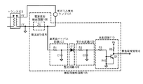
図1は、本実施形態の発明に係る放電ランプ装置の回路構成を示す図である。
同図において、1は直流電源、2は交流変換回路、21はスイッチング素子駆動回路、22はRSフリップフロップ、3はトランス、4は希ガス蛍光ランプ、5は無負荷検知回路、51はトランス3の2次側を流れる電流を検出する電流波形検出回路、52はスイッチ回路、53は平均化回路、54は比較回路である。
A first embodiment of the present invention will be described with reference to FIGS.
FIG. 1 is a diagram showing a circuit configuration of a discharge lamp device according to the invention of this embodiment.
In the figure, 1 is a DC power supply, 2 is an AC conversion circuit, 21 is a switching element drive circuit, 22 is an RS flip-flop, 3 is a transformer, 4 is a rare gas fluorescent lamp, 5 is a no-load detection circuit, and 51 is a transformer 3. , A current waveform detection circuit for detecting a current flowing through the secondary side, 52 a switch circuit, 53 an averaging circuit, and 54 a comparison circuit.
図2は、図1に示した希ガス蛍光ランプ4の構成を示す図であり、図2(a)は、希ガス蛍光ランプの管軸方向に直交する切断面から見た断面図、図2(b)は、希ガス蛍光ランプの斜視図である。
これらの図に示すように、希ガス蛍光ランプ4は、例えば、ガラス管41にて密閉状に構成された直管状の外囲器であって、その内面には希土類蛍光体、ハロリン酸塩蛍光体等の蛍光体よりなる蛍光物質42が形成されている。ガラス管41の封着構造はガラス管41の端部にディスク状の封着ガラス板を封着して構成されているが、例えば、単にガラス管41を加熱しながら縮径加工し溶断するいわゆるトップシールによって構成することもできる。外部電極43、44は、例えば、アルミニウムテープを幅1mmに切断したものが、ガラス管41の外表面における希ガス蛍光ランプの中心軸を挟んだ対向位置に貼り付けられている。また、外部電極43、44は、例えば、導電性ペーストをスクリーン印刷し、焼付けて形成したものであってもよい。なお、このガラス管41の密閉空間には水銀等の金属蒸気を含まないHe、Ar、Xe、Krのいずれか1種類以上を主成分とする希ガスが所定量封入されている。易始動部位45は、導電性物質もしくは易電子放射物質よりなり、放電開始を容易にするために、ガラス管41の内部に少なくとも1箇所配置される。放電は易始動部位45を起点に発生し、そこから連鎖的に希ガス蛍光ランプ全体に広がる。通常は、ガラス管41の端部等に設けられ、点灯中における光取出効率に影響を与えないようにする。
FIG. 2 is a diagram showing the configuration of the rare
As shown in these drawings, the rare
図3は、希ガス蛍光ランプ4の等価回路を示す図である。
同図に示すように、希ガス蛍光ランプ4は、ガラス管41の静電容量Cgと、放電のインピーダンスpが直列に接続され、放電空間の静電容量Cdが放電のインピーダンスpと並列に接続された形で表される。静電容量Csはハーネスやトランス等の浮遊容量である。このように、希ガス蛍光ランプ4は、ガラス管41の静電容量を介して放電する、容量性の負荷である。無負荷時は、放電のインピーダンスpは無限大になるので、希ガス蛍光ランプ4はコンデンサと等価とみなせる。
FIG. 3 is a diagram showing an equivalent circuit of the rare
As shown in the figure, in the rare
次に、図1に戻り、本実施形態の放電ランプ装置の回路構成を詳しく説明する。
同図において、直流電源1から出力される直流電圧は、交流変換回路2に入力される。交流変換回路2は、スイッチング素子Q11、Q12、Q21、Q22、ダイオードD11、D12、D21、D22からなり、フルブリッジ回路を構成する。スイッチング素子Q11、Q22と、スイッチング素子Q21、Q12は、各々直列に接続され、それらの両端に直流電源1が接続される。スイッチング素子Q11、Q21はハイサイド側に配置され、スイッチング素子Q22、Q12はローサイド側に配置される。ダイオードD11〜D22は、各々スイッチング素子Q11〜Q22の寄生ダイオード、または別に付加したものであり、スイッチング素子Q11、Q12、Q21、Q22に対して、各々個別に並列接続される。方向は低電位側から高電位側を順方向とする。スイッチング素子Q11、Q12、Q21、Q22には、スイッチング素子駆動回路21から出力される信号S1、S1、S2、S2が各々入力され、同信号がハイレベルの場合にオンとなり、ローレベルの場合にオフとなるように動作する。トランス3の1次側両端には、交流変換回路2のスイッチング素子Q11、Q22の接続点とスイッチング素子Q21、Q12の接続点に接続され、トランス3の2次側両端には、希ガス蛍光ランプ4と無負荷検知回路5の電流波形検出回路51とからなる直列回路が接続される。無負荷検知回路5から出力された無負荷検知信号は、スイッチング素子駆動回路21に入力される。
Next, returning to FIG. 1, the circuit configuration of the discharge lamp device of the present embodiment will be described in detail.
In the figure, the DC voltage output from the
同図において、スイッチング素子Q11、Q12を第1のスイッチング素子とし、スイッチング素子Q21、Q22を第2のスイッチング素子とする。また、第1のスイッチング素子Q11、Q12がオンの時に電流が流れる経路を第1の電流経路とし、具体的には、直流電源1の高電位側から、スイッチング素子Q11、トランス3の1次側、スイッチング素子Q12、直流電源1の低電位側までを周回する経路と、トランス3の2次側の高電位端子(以下、HV端子という)から、希ガス蛍光ランプ4、無負荷検知回路5の電流波形検出回路51、トランス3の低電位端子(以下、LV端子という)までを周回する経路とする。また、第2のスイッチング素子Q21、Q22がオンの時に電流が流れる経路を第2の電流経路とし、具体的には、直流電源1の高電位側から、スイッチング素子Q21、トランス3の1次側、スイッチング素子Q22、直流電源1の低電位側までを周回する経路と、トランス3の2次側のLV端子から、無負荷検知回路5の電流波形検出回路51、希ガス蛍光ランプ4、トランス3の2次側のHV端子までを周回する経路とする。
In the figure, switching elements Q11 and Q12 are first switching elements, and switching elements Q21 and Q22 are second switching elements. Further, a path through which a current flows when the first switching elements Q11 and Q12 are on is defined as a first current path. Specifically, from the high potential side of the
ここで、無負荷検知回路5の電流波形検出回路51は、第1の電流経路と第2の電流経路が重なり、かつ第1のスイッチング素子がオンになって最初に流れる電流の方向と、第2のスイッチング素子がオンになって最初に流れる電流の方向とが互いに逆となる経路内であればどこに設けても良い。 Here, the current waveform detection circuit 51 of the no-load detection circuit 5 includes a first current path and a second current path that overlap each other and the first switching element is turned on, As long as it is in the path | route where the direction of the electric current which flows initially when the switching element of 2 is turned on mutually reverses, you may provide.
図4は、図1に示した無負荷検知回路5の具体的構成を示す回路図である。
同図において、電流波形検出回路51は抵抗Rsからなり、電流に比例した大きさの電流波形信号を出力する。電流経路が接地できない場合は抵抗Rsの代わりにカレントトランスを用いても良い。電流波形信号はスイッチ回路52に入力される。スイッチ回路52に入力される入力信号は、一端が直流電圧Vaに接続された抵抗R1、R2の直列回路の他端へ接続される。抵抗R1とR2の接続点は、スイッチAS1の一端へ接続される。ここでは、単電源入力のアナログスイッチを用いるため、電流波形信号のゼロ点をR2×Va/(R1+R2)とし、振動波形が正の範囲に収まるように調節されている。ただし、R1、R2≫Rsとする。スイッチAS1には制御信号として図1に示したRSフリップフロップ22からスイッチ回路制御信号が入力され、スイッチ回路制御信号がハイレベルの場合に導通状態となり、ローレベルの場合に非導通状態となる。スイッチ回路52の出力信号は、平均化回路53へ入力される。平均化回路53に入力される入力信号は、一端が接地されたコンデンサC1の他端に入力され、平均化される。平均化された信号は、比較回路54へ入力される。比較回路54は、オペアンプOP1,抵抗R3〜R11、トランジスタQ1、直流電圧Vaから構成される。比較回路54へ入力された信号は、スイッチ回路52でシフトしたゼロ点を元に戻すための差動増幅回路へ入力される。差動増幅回路は、抵抗R3、R4、R7、R8とオペアンプから構成され、R3=R7、R4=R8の関係である。差動増幅回路のプラス入力側(R3側)には、コンデンサC1で平均化された信号が入力され、マイナス入力側(R7側)には、電圧Vaを抵抗R5、R6により分圧した大きさの電圧が入力される。ここで、R5=R1、R6=R2とすることにより、電圧Vaの大きさが変化しても、電流波形信号のゼロ点をシフトする大きさと元に戻す大きさが同じになるので、電圧Vaのバラツキをキャンセルすることができる。差動増幅回路の出力信号、すなわちオペアンプOP1の出力信号は、抵抗R9、R10の直列回路へ入力され、抵抗R9とR10で分圧された電圧がトランジスタQ1のベース、エミッタ間に入力される。ベース、エミッタ間電圧が約0.6Vを上回ると、トランジスタQ1がオンになり、無負荷検知信号をハイレベルからローレベルに変化させる。図1において、無負荷検知信号がローレベルの時は、スイッチング素子駆動回路21の発振を持続するように働き、無負荷検知信号がハイレベルの場合は、スイッチング素子駆動回路21の発振を停止するように働く。
FIG. 4 is a circuit diagram showing a specific configuration of the no-load detection circuit 5 shown in FIG.
In the figure, a current waveform detection circuit 51 is composed of a resistor Rs and outputs a current waveform signal having a magnitude proportional to the current. If the current path cannot be grounded, a current transformer may be used instead of the resistor Rs. The current waveform signal is input to the switch circuit 52. The input signal input to the switch circuit 52 is connected to the other end of the series circuit of the resistors R1 and R2 having one end connected to the DC voltage Va. A connection point between the resistors R1 and R2 is connected to one end of the switch AS1. Here, since an analog switch with a single power supply is used, the zero point of the current waveform signal is set to R2 × Va / (R1 + R2), and the vibration waveform is adjusted so as to be within a positive range. However, R1, R2 >> Rs. A switch circuit control signal is input to the switch AS1 from the RS flip-flop 22 shown in FIG. 1 as a control signal. When the switch circuit control signal is at a high level, the switch AS1 is turned on, and when the switch circuit control signal is at a low level, the switch AS1 is turned off. The output signal of the switch circuit 52 is input to the averaging circuit 53. The input signal input to the averaging circuit 53 is input to the other end of the capacitor C1 whose one end is grounded and averaged. The averaged signal is input to the comparison circuit 54. The comparison circuit 54 includes an operational amplifier OP1, resistors R3 to R11, a transistor Q1, and a DC voltage Va. The signal input to the comparison circuit 54 is input to a differential amplifier circuit for restoring the zero point shifted by the switch circuit 52. The differential amplifier circuit includes resistors R3, R4, R7, and R8 and an operational amplifier, and has a relationship of R3 = R7 and R4 = R8. A signal averaged by the capacitor C1 is input to the positive input side (R3 side) of the differential amplifier circuit, and the voltage Va is divided by the resistors R5 and R6 on the negative input side (R7 side). Is input. Here, by setting R5 = R1 and R6 = R2, even if the magnitude of the voltage Va changes, the magnitude of shifting the zero point of the current waveform signal is the same as the magnitude of returning the voltage Va, so the voltage Va This variation can be canceled. An output signal of the differential amplifier circuit, that is, an output signal of the operational amplifier OP1 is input to a series circuit of resistors R9 and R10, and a voltage divided by the resistors R9 and R10 is input between the base and emitter of the transistor Q1. When the base-emitter voltage exceeds about 0.6 V, the transistor Q1 is turned on, and the no-load detection signal is changed from the high level to the low level. In FIG. 1, when the no-load detection signal is at a low level, the switching element drive circuit 21 is kept oscillating. When the no-load detection signal is at a high level, the oscillation of the switching element drive circuit 21 is stopped. To work.
図5は、図1に示した放電ランプ装置の回路動作を説明するためのタイミングチャートである。
同図において、信号S1は、パルス幅tonのハイレベル信号が周期Tで繰り返される、繰り返し信号である。信号S2もパルス幅ton、周期Tの繰り返し信号であり、信号S1に対して位相が180°ずれて出力される。スイッチ回路制御信号は、信号S1がハイレベルになってから、信号S2がハイレベルになるまでの間がハイレベルで、信号S2がハイレベルになってから、信号S1がハイレベルになるまでの間がローレベルとなる信号である。希ガス蛍光ランプ4のランプ電圧波形は、信号S1がハイレベルになると負から正に極性反転し、信号S2がハイレベルになると正から負に極性反転する。ここで、電流波形検出回路51によって検出される電流波形信号は、第1、第2の電流経路を流れる電流に比例する信号である。電流波形信号がスイッチ回路52によって制御され平均化回路53に入力される入力信号は、スイッチ回路制御信号がハイレベルの間だけを抜き出した電流波形信号に相当する。なお、本実施形態では、スイッチ回路制御信号は、信号S1がハイレベルになってから、信号S2がハイレベルになるまでの間がハイレベルで、信号S2がハイレベルになってから、信号S1がハイレベルになるまでの間がハイレベルになるように制御されているが、スイッチ回路制御信号のオン期間は、信号S1のオン期間を全て含む、凡そ半周期(T/2)の期間であれば、これに限定する必要は無い。
FIG. 5 is a timing chart for explaining the circuit operation of the discharge lamp device shown in FIG.
In the figure, a signal S1 is a repetitive signal in which a high level signal having a pulse width ton is repeated in a cycle T. The signal S2 is also a repetitive signal having a pulse width ton and a period T, and is output with a phase shifted by 180 ° with respect to the signal S1. The switch circuit control signal is high level from the time when the signal S1 becomes high level to the time when the signal S2 becomes high level, and after the signal S2 becomes high level until the signal S1 becomes high level. It is a signal that becomes a low level. The lamp voltage waveform of the rare
次に、本発明の第2の実施形態を図6ないし図8を用いて説明する。
図6は、本実施形態の発明に係る放電ランプ装置の回路構成を示す図である。なお、同図において、無負荷検知回路6の構成および回路への挿入位置以外は、図1に示した同符号の構成に対応するので説明は省略する。
同図において、スイッチング素子Q11、Q12を第1のスイッチング素子とし、スイッチング素子Q21、Q22を第2のスイッチング素子とする。第1のスイッチング素子Q11、Q12がオンの時に電流が流れる経路を第1の電流経路とし、具体的には、直流電源1の高電位側から、スイッチング素子Q11、トランス3の1次側、スイッチング素子Q12、無負荷検知回路6の電流波形検出回路61、直流電源1の低電位側までを周回する経路と、トランス3の2次側のHV端子から、希ガス蛍光ランプ4、トランス3のLV端子までを周回する経路とする。また、第2のスイッチング素子Q21、Q22がオンの時に電流が流れる経路を第2の電流経路とし、具体的には、直流電源1の高電位側から、スイッチング素子Q21、トランス3の1次側、スイッチング素子Q22、直流電源1の低電位側までを周回する経路と、トランス3の2次側のLV端子から、希ガス蛍光ランプ4、トランス3の2次側のHV端子までを周回する経路とする。
Next, a second embodiment of the present invention will be described with reference to FIGS.
FIG. 6 is a diagram showing a circuit configuration of the discharge lamp device according to the invention of the present embodiment. In the figure, the configuration other than the configuration of the no-load detection circuit 6 and the insertion position in the circuit corresponds to the configuration of the same symbol shown in FIG.
In the figure, switching elements Q11 and Q12 are first switching elements, and switching elements Q21 and Q22 are second switching elements. A path through which current flows when the first switching elements Q11 and Q12 are on is defined as a first current path. Specifically, from the high potential side of the
同図において、無負荷検知回路6の電流波形検出回路61は、第1の電流経路に設けられているが、第1の電流経路と第2の電流経路が互いに重ならない経路内であればどこでも良い。 In the figure, the current waveform detection circuit 61 of the no-load detection circuit 6 is provided in the first current path. However, the current waveform detection circuit 61 is provided anywhere in the path where the first current path and the second current path do not overlap each other. good.
図7は、図6に示した無負荷検知回路6の具体的構成を示す回路図である。
同図において、電流波形検出回路61は抵抗Rsからなり、電流に比例した大きさの電流波形信号を出力する。電流経路が接地できない場合は抵抗Rsの代わりにカレントトランスを用いても良い。電流波形検出回路61からの出力信号は、抵抗R1、コンデンサC1からなる平均化回路62に入力され、平均化される。平均化回路62からの出力信号は、比較回路63に入力される。比較回路63に入力された入力信号は、抵抗R2、R3の直列回路へ入力され、抵抗R2とR3で分圧された電圧がトランジスタQ1のベース、エミッタ間に入力される。ベース、エミッタ間電圧が約0.6Vを上回ると、トランジスタQ1がオンになり、無負荷検知信号をハイレベルからローレベルへ変化させる。
FIG. 7 is a circuit diagram showing a specific configuration of the no-load detection circuit 6 shown in FIG.
In the figure, a current waveform detection circuit 61 is composed of a resistor Rs and outputs a current waveform signal having a magnitude proportional to the current. If the current path cannot be grounded, a current transformer may be used instead of the resistor Rs. The output signal from the current waveform detection circuit 61 is input to an averaging circuit 62 composed of a resistor R1 and a capacitor C1, and is averaged. An output signal from the averaging circuit 62 is input to the comparison circuit 63. The input signal input to the comparison circuit 63 is input to the series circuit of the resistors R2 and R3, and the voltage divided by the resistors R2 and R3 is input between the base and emitter of the transistor Q1. When the base-emitter voltage exceeds about 0.6 V, the transistor Q1 is turned on, and the no-load detection signal is changed from the high level to the low level.
図8は、図6に示した放電ランプ装置の回路動作を説明するためのタイミングチャートである。
同図において、信号S1は、パルス幅tonのハイレベル信号が周期Tで繰り返される、繰り返し信号である。信号S2もパルス幅ton、周期Tの繰り返し信号であり、信号S1に対して位相が180°ずれて出力される。ランプ電圧波形は、信号S1がハイレベルになると負から正に極性反転し、信号S2がハイレベルになると正から負に極性反転する。ここで、電流波形検出回路61によって検出される電流波形信号は、第1または第2の電流経路の何れか一方の電流に比例する信号である。
FIG. 8 is a timing chart for explaining the circuit operation of the discharge lamp device shown in FIG.
In the figure, a signal S1 is a repetitive signal in which a high level signal having a pulse width ton is repeated in a cycle T. The signal S2 is also a repetitive signal having a pulse width ton and a period T, and is output with a phase shifted by 180 ° with respect to the signal S1. The ramp voltage waveform reverses in polarity from negative to positive when the signal S1 goes high, and reverses in polarity from positive to negative when the signal S2 goes high. Here, the current waveform signal detected by the current waveform detection circuit 61 is a signal proportional to the current in one of the first and second current paths.
次に、本発明の第3の実施形態を図9および図10を用いて説明する。
図9は、本実施形態の発明に係る放電ランプ装置の回路構成を示す図である。なお、同図において、無負荷検知回路7の構成および回路への挿入位置以外は、図1に示した同符号の構成に対応するので説明を省略する。また、無負荷検知回路7の具体的構成は、図7において説明した回路図と同様であるので説明を省略する。
同図において、スイッチング素子Q11、Q12を第1のスイッチング素子とし、スイッチング素子Q21、Q22を第2のスイッチング素子とする。また、第1のスイッチング素子Q11、Q12がオンの時に電流が流れる経路を第1の電流経路とし、具体的には、直流電源1の高電位側から、スイッチング素子Q11、トランス3の1次側、スイッチング素子Q12、無負荷検知回路7の電流波形検出回路71、直流電源1の低電位側までを周回する経路と、トランス3の2次側のHV端子から、希ガス蛍光ランプ4、トランス3のLV端子までを周回する経路とする。また、第2のスイッチング素子Q21、Q22がオンの時に電流が流れる経路を第2の電流経路とし、具体的には、直流電源1の高電位側から、スイッチング素子Q21、トランス3の1次側、スイッチング素子Q22、無負荷検知回路7の電流波形検出回路71、直流電源1の低電位側までを周回する経路と、トランス3の2次側のLV端子から、希ガス蛍光ランプ4、トランス3の2次側のHV端子までを周回する経路とする。
Next, a third embodiment of the present invention will be described with reference to FIGS.
FIG. 9 is a diagram showing a circuit configuration of the discharge lamp device according to the invention of the present embodiment. In the figure, the configuration other than the configuration of the no-load detection circuit 7 and the insertion position in the circuit corresponds to the configuration of the same reference numeral shown in FIG. The specific configuration of the no-load detection circuit 7 is the same as the circuit diagram described in FIG.
In the figure, switching elements Q11 and Q12 are first switching elements, and switching elements Q21 and Q22 are second switching elements. Further, a path through which a current flows when the first switching elements Q11 and Q12 are on is defined as a first current path. Specifically, from the high potential side of the
同図において、無負荷検知回路7の電流波形検出回路71は、第1の電流経路と第2の電流経路が重なり、かつ、第1のスイッチング素子がオンになって最初に流れる電流の方向と、第2のスイッチング素子がオンになって最初に流れる電流の方向が互いに同じとなる経路内であれば、どこでも良い。 In the figure, the current waveform detection circuit 71 of the no-load detection circuit 7 includes a first current path and a second current path that overlap each other, and the first switching element is turned on and the direction of the current that flows first. As long as it is in a path in which the directions of the first flowing currents are the same with each other when the second switching element is turned on, it may be anywhere.
図10は、図9に示した放電ランプ装置の回路動作を説明するためのタイミングチャートである。
同図において、信号S1は、パルス幅tonのハイレベル信号が周期Tで繰り返される、繰り返し信号である。信号S2もパルス幅ton、周期Tの繰り返し信号であり、信号S1に対して位相が180°ずれて出力される。ランプ電圧波形は、信号S1がハイレベルになると負から正に極性反転し、信号S2がハイレベルになると正から負に極性反転する。ここで、電流波形検出回路71によって検出される電流波形信号は、第1、第2の電流経路を流れる電流に比例する信号である。
FIG. 10 is a timing chart for explaining the circuit operation of the discharge lamp device shown in FIG.
In the figure, a signal S1 is a repetitive signal in which a high level signal having a pulse width ton is repeated in a cycle T. The signal S2 is also a repetitive signal having a pulse width ton and a period T, and is output with a phase shifted by 180 ° with respect to the signal S1. The ramp voltage waveform reverses in polarity from negative to positive when the signal S1 goes high, and reverses in polarity from positive to negative when the signal S2 goes high. Here, the current waveform signal detected by the current waveform detection circuit 71 is a signal proportional to the current flowing through the first and second current paths.
次に、第1ないし第3の実施形態の発明に係る放電ランプ装置における、希ガス蛍光ランプ4の点灯時および無負荷時における各部の電流波形について説明する。
図11(a)は、第1ないし第3の実施形態の発明に係る放電ランプ装置における、希ガス蛍光ランプ4の点灯時におけるトランス3の2次側に流れる電流波形を示す図である。
図11(b)は、第1ないし第3の実施形態の発明に係る放電ランプ装置における、希ガス蛍光ランプ4の無負荷時におけるトランス3の2次側に流れる電流波形を示す図である。
Next, in the discharge lamp device according to the inventions of the first to third embodiments, the current waveform of each part when the rare
FIG. 11A is a diagram showing a waveform of a current flowing on the secondary side of the transformer 3 when the rare
FIG. 11B is a diagram showing a waveform of a current flowing on the secondary side of the transformer 3 when the rare
図12(a)は、第1の実施形態(または第2の実施形態)の発明に係る放電ランプ装置の、希ガス蛍光ランプ4の点灯時における、無負荷検知回路5の平均化回路53(または無負荷検知回路6の平均化回路62)に入力される入力信号の波形を示す図であり、周期Tで波形の時間平均を行うと、平均値はある一定以上の大きさを持つ。なお、ゼロ点をシフトしている場合は、シフトした大きさを差し引いて考える。
図12(b)は、第1の実施形態(または第2の実施形態)の発明に係る放電ランプ装置の無負荷時における、無負荷検知回路5の平均化回路53(または無負荷検知回路6の平均化回路62)に入力される入力信号の波形を示す図であり、無負荷時に流れる振動電流は、希ガス蛍光ランプ4の静電容量や浮遊容量を流れる振動電流である。直流成分は含まれていない。そのため、周期Tで波形の時間平均を行なうと、平均値は略0になる。なお、ゼロ点をシフトしている場合は、シフトした大きさを差し引いて考える。
FIG. 12A shows an averaging circuit 53 of the no-load detection circuit 5 (when the noble
FIG. 12B shows an averaging circuit 53 (or no-load detection circuit 6) of the no-load detection circuit 5 when the discharge lamp device according to the first embodiment (or the second embodiment) is not loaded. The oscillating current that flows during no load is the oscillating current that flows through the capacitance and stray capacitance of the noble
図13(a)は、第3の実施形態の発明に係る放電ランプ装置の、希ガス蛍光ランプ4の点灯時における、無負荷検知回路7の平均化回路72に入力される入力信号の波形を示す図であり、周期Tで波形の時間平均を行うと、平均値はある一定以上の大きさを持つ。なお、
図13(b)は、第3の実施形態の発明に係る放電ランプ装置の無負荷時における、無負荷検知回路7の平均化回路72に入力される入力信号の波形を示す図である。無負荷時に流れる振動電流は、希ガス蛍光ランプ4の静電容量や浮遊容量を流れる振動電流であり、直流成分は含まれていない。そのため、周期Tで波形の時間平均を行なうと、平均値は略0になる。
FIG. 13A shows the waveform of the input signal input to the averaging circuit 72 of the no-load detection circuit 7 when the rare
FIG. 13B is a diagram showing a waveform of an input signal inputted to the averaging circuit 72 of the no-load detection circuit 7 when the discharge lamp device according to the third embodiment of the invention is not loaded. The oscillating current that flows when there is no load is the oscillating current that flows through the capacitance and stray capacitance of the rare
上記のごとく、第1の実施形態(または第2の実施形態)の発明に係る放電ランプ装置によれば、図12(a)に示すように、点灯時の無負荷検知回路5の平均化回路53(または無負荷検知回路6の平均化回路62)の出力はある一定以上の大きさを持ち、一方、図12(b)に示すように、無負荷時の無負荷検知回路5の平均化回路53(または無負荷時の無負荷検知回路6の平均化回路62)の出力は略0になる。この平均化回路5(または平均化回路6)の出力を測定することにより、点灯状態にあるか、無負荷状態にあるかを知ることができる。点灯時と無負荷時における平均化回路5(または平均化回路6)の出力差は大きく、区別は容易であり、また、浮遊容量等の大きさが変化し、振動電流波形の周波数が変化しても、無負荷時の積分値は略0であり、不点灯検知の正確性に影響を及ぼさない。 As described above, according to the discharge lamp device according to the invention of the first embodiment (or the second embodiment), as shown in FIG. 12A, the averaging circuit of the no-load detection circuit 5 at the time of lighting. 53 (or the averaging circuit 62 of the no-load detection circuit 6) has a certain magnitude or more, while the average of the no-load detection circuit 5 at no load is obtained as shown in FIG. The output of the circuit 53 (or the averaging circuit 62 of the no-load detection circuit 6 at no load) becomes substantially zero. By measuring the output of the averaging circuit 5 (or the averaging circuit 6), it is possible to know whether it is in the lighting state or in the no-load state. The output difference of the averaging circuit 5 (or the averaging circuit 6) when lighting and no load is large and easy to distinguish, and the size of the stray capacitance etc. changes and the frequency of the oscillating current waveform changes. However, the integrated value at the time of no load is substantially 0, and does not affect the accuracy of non-lighting detection.
また、上記のごとく、第3の実施形態の発明に係る放電ランプ装置によれば、図13(a)に示すように、点灯時の無負荷検知回路7の平均化回路72の出力はある一定以上の大きさを持ち、一方、図13(b)に示すように、無負荷時の無負荷検知回路7の平均化回路72の出力は略0になる。この平均化回路7の出力を測定することにより、点灯状態にあるか、無負荷状態にあるかを知ることができる。点灯時と無負荷時における平均化回路72の出力差は大きく、区別は容易であり、また、浮遊容量等の大きさが変化し、振動電流波形の周波数が変化しても、無負荷時の積分値は略0であり、不点灯検知の正確性に影響を及ぼさない。 Further, as described above, according to the discharge lamp device according to the invention of the third embodiment, as shown in FIG. 13A, the output of the averaging circuit 72 of the no-load detection circuit 7 during lighting is constant. On the other hand, as shown in FIG. 13B, the output of the averaging circuit 72 of the no-load detection circuit 7 at no load is substantially zero. By measuring the output of the averaging circuit 7, it is possible to know whether it is in a lighting state or in a no-load state. The output difference of the averaging circuit 72 during lighting and no load is large and easy to distinguish, and even when the size of the stray capacitance changes and the frequency of the oscillating current waveform changes, The integral value is approximately 0, and does not affect the accuracy of the non-lighting detection.
図14は、第1ないし第3の各実施形態の発明に係る放電ランプ装置の平均化回路における点灯時の時間平均値に対する無負荷時の時間平均値の相対値と、図18に示した従来技術に係る放電ランプ装置の平均化回路における、点灯時の時間平均値に対する無負荷時の時間平均値の相対値と、を示した表である。
同図に示すように、各実施形態の発明に係る放電ランプ装置においては、何れも相対値は9%台であり、点灯時と無負荷時の差は90%以上あるので、バラツキに対する許容範囲は大きい。また、浮遊容量の大きさが変化しても無負荷時の積分値の大きさに殆ど影響を及ぼさないので、点灯時と無負荷時の差が縮まることは無い。このことは、図12(a)と図12(b)、または図13(a)に示す平均化回路に入力される入力信号波形を対比観察することによっても明らかである。一方、従来技術に係る放電ランプ装置においては、相対値は65.3%であり、点灯時と無負荷時の差は約35%であるので、バラツキに対する許容範囲は小さい。また、浮遊容量等の大きさが変化すると、無負荷時の電流波形が変わり、積分値が変化するので、点灯時と無負荷時の差が縮まるおそれがある。このことは、図20(a)と図20(b)に示す平均化回路に入力される入力信号波形を対比観察することによっても明らかである。
FIG. 14 shows the relative value of the time average value during no load with respect to the time average value during lighting in the averaging circuit of the discharge lamp device according to the invention of each of the first to third embodiments, and the prior art shown in FIG. It is the table | surface which showed the relative value of the time average value at the time of no load with respect to the time average value at the time of lighting in the averaging circuit of the discharge lamp apparatus which concerns on a technique.
As shown in the figure, in the discharge lamp devices according to the embodiments of the present invention, the relative value is 9%, and the difference between lighting and no load is 90% or more. Is big. In addition, even if the size of the stray capacitance changes, there is almost no effect on the size of the integrated value when there is no load, so that the difference between lighting and no load is not reduced. This is also clear by comparing and observing the input signal waveform input to the averaging circuit shown in FIG. 12 (a) and FIG. 12 (b) or FIG. 13 (a). On the other hand, in the discharge lamp device according to the prior art, the relative value is 65.3%, and the difference between lighting and no load is about 35%, so the tolerance for variation is small. Further, when the magnitude of the stray capacitance or the like changes, the current waveform at the time of no load changes and the integrated value changes, so that the difference between lighting and no load may be reduced. This is also clear by comparing and observing the input signal waveform input to the averaging circuit shown in FIGS. 20 (a) and 20 (b).
なお、第1ないし第3の実施形態においては、交流変換回路2をフルブリッジ方式で構成したが、これに限定されず、交流変換回路2をプッシュプル方式で構成してもよい。
図15は、交流変換回路2をプッシュプル方式で構成し、無負荷検知回路が省略されて示されている放電ランプ装置の回路構成を示す図である。
同図において、ここでは、一方のスイッチング素子Q1を第1のスイッチング素子とし、他方のスイッチング素子Q2を第2のスイッチング素子とする。第1の電流経路は、第1のスイッチング素子Q1がオンの時に電流が流れる経路であり、この電流は、直流電源1の高電位側から、トランス3、スイッチング素子Q1、直流電源1の低電位側までを周回とする経路と、トランス3の2次側のHV端子から、希ガス蛍光ランプ4、トランス3の2次側のLV端子までを周回とする経路を流れる。第2の電流経路は、第2のスイッチング素子Q2がオンの時に電流が流れる経路であり、この電流は、直流電源1の高電位側から、トランス3、スイッチング素子Q2、直流電源1の低電位側までを周回とする経路と、トランス3の2次側のLV端子から、希ガス蛍光ランプ4、トランス3の2次側のHV端子までを周回とする経路を流れる。
In the first to third embodiments, the
FIG. 15 is a diagram illustrating a circuit configuration of a discharge lamp device in which the
In the figure, here, one switching element Q1 is a first switching element, and the other switching element Q2 is a second switching element. The first current path is a path through which a current flows when the first switching element Q1 is turned on. This current flows from the high potential side of the
また、交流変換回路2をハーフブリッジ方式で構成してもよい。
図16は、交流変換回路2をハーフブリッジ方式で構成し、無負荷検知回路が省略されて示されている放電ランプ装置の回路構成を示す図である。
同図において、ここでは、一方のスイッチング素子Q1を第1のスイッチング素子とし、他方のスイッチング素子Q2を第2のスイッチング素子とする。第1の電流経路は、第1のスイッチング素子Q1がオンの時に電流が流れる経路であり、この電流は、コンデンサC1の高電位側から、スイッチング素子Q1、トランス3、コンデンサC1の低電位側までを周回とする経路と、トランス3の2次側のHV端子から、希ガス蛍光ランプ4、トランス3の2次側のLV端子までを周回とする経路を流れる。第2の電流経路は、第2のスイッチング素子Q2がオンの時に電流が流れる経路であり、この電流は、コンデンサC2の高電位側から、トランス3の1次側、スイッチング素子Q2、コンデンサC2の低電位側までを周回とする経路と、トランス3の2次側のLV端子から、希ガス蛍光ランプ4、トランス3の2次側のHV端子までを周回とする経路を流れる。
Moreover, you may comprise the alternating
FIG. 16 is a diagram illustrating a circuit configuration of a discharge lamp device in which the
In the figure, here, one switching element Q1 is a first switching element, and the other switching element Q2 is a second switching element. The first current path is a path through which a current flows when the first switching element Q1 is on. This current flows from the high potential side of the capacitor C1 to the low potential side of the switching element Q1, the transformer 3, and the capacitor C1. And a path that goes around from the secondary HV terminal of the transformer 3 to the rare
図15および図16において、第1の実施形態の放電ランプ装置における無負荷検知回路5に相当する無負荷検知回路が挿入される箇所は、第1の電流経路と第2の電流経路が重なり、かつ、第1のスイッチング素子がオンになって最初に流れる電流と、第2のスイッチング素子がオンになって最初に流れる電流の方向が互いに逆となる経路内であれば、どこに設けても良い。また、第2の実施形態の放電ランプ装置における無負荷検知回路6に相当する無負荷検知回路が挿入される箇所は、第1の電流経路と第2の電流経路で互いに重ならない経路内であればどこでも良い。さらに、第3の実施形態の放電ランプ装置における無負荷検知回路7に相当する無負荷検知回路が挿入される箇所は、第1の電流経路と第2の電流経路が重なり、かつ、第1のスイッチング素子がオンになって最初に流れる電流と、第2のスイッチング素子がオンになって最初に流れる電流の方向が互いに同じとなる経路内であれば、どこに設けても良い。 In FIG. 15 and FIG. 16, the first current path and the second current path overlap at a place where a no-load detection circuit corresponding to the no-load detection circuit 5 in the discharge lamp device of the first embodiment is inserted. In addition, the first current flowing when the first switching element is turned on and the first current flowing when the second switching element is turned on may be provided anywhere as long as the directions are opposite to each other. . In addition, a place where a no-load detection circuit corresponding to the no-load detection circuit 6 in the discharge lamp device of the second embodiment is inserted may be in a path where the first current path and the second current path do not overlap each other. Anywhere. Furthermore, in the place where the no-load detection circuit corresponding to the no-load detection circuit 7 in the discharge lamp device of the third embodiment is inserted, the first current path and the second current path overlap, and the first It may be provided anywhere as long as the current flowing first after the switching element is turned on and the current flowing first after the second switching element is turned on are in the same path.
なお、本発明の放電ランプ装置は、希ガス蛍光ランプに代えて、エキシマランプにも適用可能である。
図17は、エキシマランプの一例を示す概略断面図である。同図に示すように、このエキシマランプは、円筒外部放射型のもので、放電容器46は石英ガラス等の誘電体で構成されている。放電容器46は、円筒状をした外壁461と、その内側に筒軸を共通にした円筒状の内壁462と、この外壁461と内壁462とを両端で封止する封止壁463、464からなり、これらの各壁で囲まれた円筒状の領域が放電空間Sとなる。外壁461の表面に密着して網状の第1の電極47が設けられ、内壁462の筒軸側の表面に密着してアルミニウム等からなる第2の電極48が密着して設けられている。これらの第1、第2電極間には高周波電源8が接続される。高周波電源8により第1の電極47と第2の電極48との間に高周波電圧が印加されると、放電空間S内には誘電体バリア放電による直径0.02〜0.2mm程度の多数のマイクロプラズマが発生する。これにより放電空間S内にエキシマが生成され、エキシマ光が放出される。このエキシマ光は、外壁461を透過し第1の電極47の網目を通って外部に放射される。放電空間S内に封入される放電ガスとしては、希ガスまたは希ガスとハロゲンガスとの混合ガスが用いられるが、放電ガスの種類を変えることによって、それぞれ発光中心波長が異なるエキシマ光を放射させることができる。放電ガスとして、キセノン(Xe)、クリプトン(Kr)、アルゴン(Ar)等の希ガスを用いた場合には、それぞれ172nm、146nm、126nmの発光中心波長をもつエキシマ光を得ることができる。また、クリプトン(Kr)と塩素(Cl)ガスとの混合ガスを用いた場合には、発光中心波長が222nmのエキシマ光が得られる。
The discharge lamp device of the present invention can also be applied to an excimer lamp instead of the rare gas fluorescent lamp.
FIG. 17 is a schematic cross-sectional view showing an example of an excimer lamp. As shown in the figure, this excimer lamp is of a cylindrical external radiation type, and the
1 直流電源
2 交流変換回路
21 スイッチング素子駆動回路
22 RSフリップフロップ
3 トランス
4 希ガス蛍光ランプ
41 ガラス管
42 蛍光物質
43,44 外部電極
45 易始動部位
46 放電容器
461 外壁
462 内壁
463、464 封止壁
47 第1の電極
48 第2の電極
5 無負荷検知回路
51 電流波形検出回路
52 スイッチ回路
53 平均化回路
54 比較回路
6 無負荷検知回路
61 電流波形検出回路
62 平均化回路
63 比較回路
7 無負荷検知回路
71 電流波形検出回路
72 平均化回路
73 比較回路
8 高周波電源
Q11、Q12、Q21、Q22 スイッチング素子
D11、D12、D21、D22 ダイオード
DESCRIPTION OF
61 Current waveform detection circuit 62 Averaging circuit 63 Comparison circuit 7 No load detection circuit 71 Current waveform detection circuit 72 Averaging circuit 73 Comparison circuit 8 High frequency power supplies Q11, Q12, Q21, Q22 Switching elements D11, D12, D21, D22 Diodes
Claims (6)
前記第1のスイッチング素子のオン期間を含み前記第2のスイッチング素子のオン期間を含まない前記交流電圧の略半周期間流れる電流を検出する手段と、前記検出された電流を平均化する平均化回路と、該平均化回路の出力値を基準値と比較する比較回路と、からなる無負荷検知回路を設けたことを特徴とする放電ランプ装置。 An alternating current conversion circuit for converting a direct current voltage into an alternating current voltage by alternately switching one or one set of first switching elements and the other or the other set of second switching elements; and alternating current from the alternating current conversion circuit In a discharge lamp device comprising a transformer for boosting voltage and a rare gas fluorescent lamp connected to the secondary side of the transformer,
Means for detecting a current flowing during a substantially half cycle of the AC voltage including an ON period of the first switching element and not including an ON period of the second switching element; and an averaging circuit for averaging the detected current And a no-load detection circuit comprising a comparison circuit that compares the output value of the averaging circuit with a reference value.
第1のスイッチング素子がオンの時に流れる第1の電流経路と第2のスイッチング素子がオンの時に流れる第2の電流経路とが重なると共に、前記第1の電流経路と前記第2の電流経路を流れる電流が互いに逆方向である電流経路に直列に接続された電流波形検出回路と、前記第1のスイッチング素子のオン期間を含み前記第2のスイッチング素子のオン期間を含まない前記交流電圧の略半周期間、前記電流波形検出回路で検出された電流波形信号を通過させるスイッチ回路と、該スイッチ回路を通過した電流波形信号を平均化する平均化回路と、該平均化回路の出力値を基準値と比較する比較回路と、からなる無負荷検知回路を設けたことを特徴とする放電ランプ装置。 An alternating current conversion circuit for converting a direct current voltage into an alternating current voltage by alternately switching one or one set of first switching elements and the other or the other set of second switching elements; and alternating current from the alternating current conversion circuit In a discharge lamp device comprising a transformer for boosting voltage and a rare gas fluorescent lamp connected to the secondary side of the transformer,
The first current path that flows when the first switching element is on and the second current path that flows when the second switching element are on overlap, and the first current path and the second current path are A current waveform detection circuit connected in series to current paths in which flowing currents are in opposite directions, and an abbreviation of the AC voltage that includes the ON period of the first switching element and does not include the ON period of the second switching element. A switch circuit that passes the current waveform signal detected by the current waveform detection circuit for a half cycle, an averaging circuit that averages the current waveform signal that has passed through the switch circuit, and an output value of the averaging circuit as a reference value A discharge lamp device comprising a comparison circuit for comparing with a no-load detection circuit.
第1のスイッチング素子がオンの時に流れる第1の電流経路と第2のスイッチング素子がオンの時に流れる第2の電流経路とが重ならない電流経路に直列に接続された電流波形検出回路と、前記電流波形検出回路で検出された電流波形信号を平均化する平均化回路と、該平均化回路の出力値を基準値と比較する比較回路と、からなる無負荷検知回路を設けたことを特徴とする放電ランプ装置。 An alternating current conversion circuit for converting a direct current voltage into an alternating current voltage by alternately switching one or one set of first switching elements and the other or the other set of second switching elements; and alternating current from the alternating current conversion circuit In a discharge lamp device comprising a transformer for boosting voltage and a rare gas fluorescent lamp connected to the secondary side of the transformer,
A current waveform detection circuit connected in series to a current path that does not overlap a first current path that flows when the first switching element is on and a second current path that flows when the second switching element is on; A no-load detection circuit comprising an averaging circuit that averages current waveform signals detected by the current waveform detection circuit, and a comparison circuit that compares an output value of the averaging circuit with a reference value is provided. Discharge lamp device.
第1のスイッチング素子がオンの時に流れる第1の電流経路と第2のスイッチング素子がオンの時に流れる第2の電流経路とが重なると共に、前記第1の電流経路と前記第2の電流経路を流れる電流が互いに同方向である電流経路に直列に接続された電流波形検出回路と、前記電流波形検出回路で検出された電流波形信号を平均化する平均化回路と、該平均化回路の出力値を基準値と比較する比較回路と、からなる無負荷検知回路を設けたことを特徴とする放電ランプ装置。 An alternating current conversion circuit for converting a direct current voltage into an alternating current voltage by alternately switching one or one set of first switching elements and the other or the other set of second switching elements; and alternating current from the alternating current conversion circuit In a discharge lamp device comprising a transformer for boosting voltage and a rare gas fluorescent lamp connected to the secondary side of the transformer,
The first current path that flows when the first switching element is on and the second current path that flows when the second switching element are on overlap, and the first current path and the second current path are A current waveform detection circuit connected in series to current paths in which flowing currents are in the same direction, an averaging circuit that averages the current waveform signals detected by the current waveform detection circuit, and an output value of the averaging circuit A discharge lamp device comprising a no-load detection circuit comprising a comparison circuit for comparing the voltage with a reference value.
Priority Applications (2)
| Application Number | Priority Date | Filing Date | Title |
|---|---|---|---|
| JP2008150954A JP2009295556A (en) | 2008-06-09 | 2008-06-09 | Discharge lamp device |
| KR1020090030279A KR20090127802A (en) | 2008-06-09 | 2009-04-08 | Discharge lamp device |
Applications Claiming Priority (1)
| Application Number | Priority Date | Filing Date | Title |
|---|---|---|---|
| JP2008150954A JP2009295556A (en) | 2008-06-09 | 2008-06-09 | Discharge lamp device |
Publications (1)
| Publication Number | Publication Date |
|---|---|
| JP2009295556A true JP2009295556A (en) | 2009-12-17 |
Family
ID=41543543
Family Applications (1)
| Application Number | Title | Priority Date | Filing Date |
|---|---|---|---|
| JP2008150954A Pending JP2009295556A (en) | 2008-06-09 | 2008-06-09 | Discharge lamp device |
Country Status (2)
| Country | Link |
|---|---|
| JP (1) | JP2009295556A (en) |
| KR (1) | KR20090127802A (en) |
Cited By (2)
| Publication number | Priority date | Publication date | Assignee | Title |
|---|---|---|---|---|
| JP2021052491A (en) * | 2019-09-25 | 2021-04-01 | 東芝ライテック株式会社 | Electric power supply device |
| JP2022041626A (en) * | 2020-09-01 | 2022-03-11 | ウシオ電機株式会社 | Light source device, lighting circuit, driving method |
Families Citing this family (2)
| Publication number | Priority date | Publication date | Assignee | Title |
|---|---|---|---|---|
| US10804691B2 (en) * | 2018-03-06 | 2020-10-13 | Texas Instruments Incorporated | Circuit providing reverse current protection for high-side driver |
| JP7043139B2 (en) * | 2018-06-25 | 2022-03-29 | エイブリック株式会社 | Backflow prevention circuit and power supply circuit |
Citations (7)
| Publication number | Priority date | Publication date | Assignee | Title |
|---|---|---|---|---|
| JPH03124231A (en) * | 1989-10-04 | 1991-05-27 | Hitachi Ltd | Multiplex dc power supply |
| JPH07143740A (en) * | 1993-11-12 | 1995-06-02 | Hitachi Ltd | Power supply circuit |
| JPH07274492A (en) * | 1994-03-28 | 1995-10-20 | Nippondenso Co Ltd | Dc-dc converter having fail safe function |
| JP2003347085A (en) * | 2002-05-29 | 2003-12-05 | West Electric Co Ltd | Lighting circuit for cold cathode discharge tube and illuminating device using the same |
| JP2006302563A (en) * | 2005-04-18 | 2006-11-02 | Harison Toshiba Lighting Corp | Discharge lamp lighting device |
| JP2007336636A (en) * | 2006-06-13 | 2007-12-27 | Mitsumi Electric Co Ltd | Multiple-output dc-dc converter |
| JP2008109815A (en) * | 2006-10-27 | 2008-05-08 | Daihen Corp | High-frequency power supply unit |
-
2008
- 2008-06-09 JP JP2008150954A patent/JP2009295556A/en active Pending
-
2009
- 2009-04-08 KR KR1020090030279A patent/KR20090127802A/en not_active Application Discontinuation
Patent Citations (7)
| Publication number | Priority date | Publication date | Assignee | Title |
|---|---|---|---|---|
| JPH03124231A (en) * | 1989-10-04 | 1991-05-27 | Hitachi Ltd | Multiplex dc power supply |
| JPH07143740A (en) * | 1993-11-12 | 1995-06-02 | Hitachi Ltd | Power supply circuit |
| JPH07274492A (en) * | 1994-03-28 | 1995-10-20 | Nippondenso Co Ltd | Dc-dc converter having fail safe function |
| JP2003347085A (en) * | 2002-05-29 | 2003-12-05 | West Electric Co Ltd | Lighting circuit for cold cathode discharge tube and illuminating device using the same |
| JP2006302563A (en) * | 2005-04-18 | 2006-11-02 | Harison Toshiba Lighting Corp | Discharge lamp lighting device |
| JP2007336636A (en) * | 2006-06-13 | 2007-12-27 | Mitsumi Electric Co Ltd | Multiple-output dc-dc converter |
| JP2008109815A (en) * | 2006-10-27 | 2008-05-08 | Daihen Corp | High-frequency power supply unit |
Cited By (4)
| Publication number | Priority date | Publication date | Assignee | Title |
|---|---|---|---|---|
| JP2021052491A (en) * | 2019-09-25 | 2021-04-01 | 東芝ライテック株式会社 | Electric power supply device |
| JP7331582B2 (en) | 2019-09-25 | 2023-08-23 | 東芝ライテック株式会社 | power supply |
| JP2022041626A (en) * | 2020-09-01 | 2022-03-11 | ウシオ電機株式会社 | Light source device, lighting circuit, driving method |
| JP7449474B2 (en) | 2020-09-01 | 2024-03-14 | ウシオ電機株式会社 | Light source device, lighting circuit, driving method |
Also Published As
| Publication number | Publication date |
|---|---|
| KR20090127802A (en) | 2009-12-14 |
Similar Documents
| Publication | Publication Date | Title |
|---|---|---|
| JP4118941B2 (en) | Dielectric barrier discharge lamp lighting device and method for detecting the number of lighting of dielectric barrier discharge lamp | |
| JP2009295556A (en) | Discharge lamp device | |
| WO2003009649A1 (en) | Dielectric barrier discharge lamp operating device | |
| WO2005104631A1 (en) | Lighting system | |
| JP2003100482A (en) | Dielectric barrier discharge lamp lighting device | |
| US7429829B2 (en) | Discharge lamp lighting circuit with an open protection circuit | |
| WO2008029445A1 (en) | Discharge lamp lighting apparatus | |
| JP2005174909A (en) | Backlight unit | |
| US7271547B2 (en) | High-pressure discharge lamp having a pulse starting device, and operating method for a high pressure discharge lamp | |
| US7109666B2 (en) | Lighting device for a dielectric barrier discharge lamp | |
| JP2006012660A (en) | Discharge lamp lighting circuit | |
| JP2002134293A (en) | Back light equipment | |
| JP2009009721A (en) | Discharge lamp lighting device | |
| KR101181142B1 (en) | Lighting apparatus for rare gas fluorescent lamp | |
| JP3988341B2 (en) | Noble gas fluorescent lamp lighting device | |
| JP4690296B2 (en) | Discharge lamp lighting device | |
| JP2003077691A (en) | High pressure discharge lamp lighting device and floodlight device | |
| EP1635622A1 (en) | Electric discharge lamp operating device | |
| JP2007265897A (en) | Inverter circuit for discharge tube | |
| JP2008091313A (en) | Lighting system, and protection method of hot-cathode fluorescent tube | |
| KR20060050232A (en) | Method and apparatus for driving a discharge lamp in a floating configuration | |
| JP2006134837A (en) | Discharge lamp driving device and liquid crystal display | |
| JP4703626B2 (en) | Discharge lamp lighting device | |
| CN101161038A (en) | Device and method for driving a high-pressure discharge lamp | |
| JP2003217886A (en) | Discharge lamp lighting device and image reading device built-in device |
Legal Events
| Date | Code | Title | Description |
|---|---|---|---|
| A621 | Written request for application examination |
Free format text: JAPANESE INTERMEDIATE CODE: A621 Effective date: 20110317 |
|
| A977 | Report on retrieval |
Free format text: JAPANESE INTERMEDIATE CODE: A971007 Effective date: 20120820 |
|
| A131 | Notification of reasons for refusal |
Free format text: JAPANESE INTERMEDIATE CODE: A131 Effective date: 20120919 |
|
| A02 | Decision of refusal |
Free format text: JAPANESE INTERMEDIATE CODE: A02 Effective date: 20130529 |