JP2009135195A - Light emitting device - Google Patents
Light emitting device Download PDFInfo
- Publication number
- JP2009135195A JP2009135195A JP2007308814A JP2007308814A JP2009135195A JP 2009135195 A JP2009135195 A JP 2009135195A JP 2007308814 A JP2007308814 A JP 2007308814A JP 2007308814 A JP2007308814 A JP 2007308814A JP 2009135195 A JP2009135195 A JP 2009135195A
- Authority
- JP
- Japan
- Prior art keywords
- solder
- light emitting
- emitting device
- cup member
- pattern
- Prior art date
- Legal status (The legal status is an assumption and is not a legal conclusion. Google has not performed a legal analysis and makes no representation as to the accuracy of the status listed.)
- Granted
Links
Images


Classifications
-
- H10W90/754—
Landscapes
- Led Device Packages (AREA)
Abstract
Description
本発明は、基板上に発光ダイオード(以下、LEDと記す。)チップなどの発光素子を配置した発光装置に関する。 The present invention relates to a light emitting device in which a light emitting element such as a light emitting diode (hereinafter referred to as LED) chip is arranged on a substrate.
LEDを用いた表示装置や照明器具は、光取り出し効率の向上や、LED素子を封止する際に用いる樹脂の溜め(硬化前の樹脂液の溜め)を目的として、カップ形状が良く使われる。例を挙げると、特許文献1,2に開示された技術が挙げられる。
For display devices and lighting fixtures using LEDs, cup shapes are often used for the purpose of improving the light extraction efficiency and storing the resin used to seal the LED elements (reserving the resin liquid before curing). For example, the techniques disclosed in
図1は、特許文献1の実施例に記載された照明装置を示す図である。この照明装置は、回路基板1上に絶縁層2が設けられ、この絶縁層2上に配線3が設けられ、この配線3を設けた部分にLEDチップ5が実装され、LEDチップ5を囲むようにカップ形状を持った基台4が接合され、さらに基台4の開口にカバー6を設けた構成になっている。
FIG. 1 is a diagram illustrating an illuminating device described in an embodiment of Patent Document 1. In FIG. In this lighting device, an
図2は、特許文献2の実施例に記載された照明装置を示す図である。この照明装置は、絶縁基体8に配線層7が設けられ、上側の配線層7にLEDチップ9が実装され、該LEDチップ9の上側電極が他の配線層7に導電性ワイヤ10で接続され、LEDチップ9の周囲に枠体11を配置した構成になっている。
しかしながら、特許文献1,2に開示された従来技術には、次のような問題がある。
特許文献1には、基台4の材質について特に記載は無いが、配線3の直上に設置されていることから絶縁層と考えられる。また、基台4の固定方法についても特に記載はない。一般的には接着剤などを用いると考えられる。その場合、接合部の信頼性に不安が生じる。また、接着剤の塗布、硬化など、工程が煩雑になり、生産性が低い。
However, the conventional techniques disclosed in
In Patent Document 1, although there is no particular description about the material of the
また、特許文献2の実施例において、絶縁基体8はセラミックグリーンシート積層法により作られている。枠体11は金属製であり、LEDチップ9からの光を反射し、効率良く光を外部へ取り出す目的で嵌着されている。ベースとなる絶縁基体8と、LED収納部を形成する絶縁基体8は、焼成により強固に接合することができるが、枠体11は嵌め込まれただけであり、振動などにより欠落する恐れがある。また、嵌め込み構造を作る必要があるため、生産性も良いとは言えない。
Moreover, in the Example of
本発明は、前記事情に鑑みてなされ、容易に製造することができ、接着剤などの従来方法による固定よりも信頼性の高い固定方式によりカップ部材を固定し得るLEDチップなどの発光素子を用いる発光装置の提供を目的とする。 The present invention is made in view of the above circumstances, and uses a light emitting element such as an LED chip that can be easily manufactured and can fix a cup member by a fixing method that is more reliable than fixing by a conventional method such as an adhesive. An object is to provide a light-emitting device.
前記目的を達成するため、本発明は、基板上に少なくとも1つ以上の発光素子が配置され、該発光素子の周囲の基板上に半田パターンが形成され、該半田パターン上にカップ部材が半田により固定されていることを特徴とする発光装置を提供する。 In order to achieve the above object, according to the present invention, at least one light emitting element is disposed on a substrate, a solder pattern is formed on a substrate around the light emitting element, and a cup member is formed on the solder pattern by soldering. Provided is a light-emitting device that is fixed.
また本発明は、基板上に少なくとも1つ以上の発光素子が配置され、発光素子を囲むように基板上に半田パターンが形成され、前記半田パターンの少なくとも1箇所に切欠があり、前記切欠の少なくとも1つに、少なくとも1本の配線パターンが通り、前記半田パターン上にカップ部材が半田により固定されていることを特徴とする発光装置を提供する。 According to the present invention, at least one light emitting element is disposed on the substrate, a solder pattern is formed on the substrate so as to surround the light emitting element, and there is a notch in at least one position of the solder pattern. One is a light-emitting device characterized in that at least one wiring pattern passes and a cup member is fixed on the solder pattern by solder.
また本発明は、基板上に少なくとも1つ以上の発光素子が配置され、発光素子を囲むように基板上に半田パターンが形成され、前記半田パターンの少なくとも1箇所に切り欠きがあり、前記切り欠きの少なくとも1つに、少なくとも1本の配線パターンが通り、前記配線パターンの少なくとも一部に絶縁層があり、前記半田パターン上にカップ部材が半田により固定されていることを特徴とする発光装置を提供する。 According to the present invention, at least one light emitting element is disposed on the substrate, a solder pattern is formed on the substrate so as to surround the light emitting element, and there is a notch in at least one portion of the solder pattern. A light emitting device, wherein at least one wiring pattern passes through at least one of the wiring patterns, an insulating layer is provided on at least a part of the wiring pattern, and a cup member is fixed on the solder pattern by solder. provide.
前記発光装置において、切欠が等角度に配置され、分割された半田パターンが同形をなしていることが好ましい。 In the light emitting device, it is preferable that the notches are arranged at an equal angle and the divided solder patterns have the same shape.
また本発明は、基板上に少なくとも1つ以上の発光素子が配置され、基板上に半田パターンがあり、配線パターンの少なくとも一部が絶縁層でカバーされ、少なくとも一部が前記絶縁層上にかかるように半田パターンが形成され、前記半田パターン上にカップ部材が半田で固定されていることを特徴とする発光装置を提供する。 In the present invention, at least one light emitting element is disposed on a substrate, a solder pattern is provided on the substrate, at least a part of the wiring pattern is covered with an insulating layer, and at least a part is over the insulating layer. Thus, a light emitting device is provided in which a solder pattern is formed and a cup member is fixed on the solder pattern with solder.
本発明の発光装置において、半田パターンに半田溜が設けられていることが好ましい。 In the light emitting device of the present invention, it is preferable that a solder reservoir is provided in the solder pattern.
本発明の発光装置において、カップ部材が半田付けされている半田パターンが、カップ部材より発光素子側に突出して設けられていることが好ましい。 In the light emitting device of the present invention, it is preferable that the solder pattern to which the cup member is soldered is provided so as to protrude from the cup member to the light emitting element side.
本発明の発光装置において、線状の部材を曲げ、両端を密接させ、カップ部材を構成してもよい。 In the light-emitting device of the present invention, the cup member may be configured by bending a linear member and bringing both ends into close contact.
本発明の発光装置において、カップ部材内部に透光性樹脂を充填したことが好ましい。
また、この透光性樹脂に光拡散物、又は蛍光体が入っている構成としてもよい。
In the light emitting device of the present invention, it is preferable that a translucent resin is filled in the cup member.
Moreover, it is good also as a structure by which the light diffusing material or fluorescent substance is contained in this translucent resin.
本発明の発光装置は、半田によりカップ部材を固定しているので、接着剤などの従来方法による固定方法よりも信頼性が高くなる。
本発明の発光装置は、半田によりカップ部材を固定しているので、外力による変形が小さくなり、カップ部材内部の構造物への影響が小さくなる。
本発明の発光装置は、半田によりカップ部材を固定しているので、他の電子部品と同時に半田ペースト印刷・リフロー実装することが可能になり、カップ固定のための特別な工程・設備を省くことができる。このことにより、発光装置の生産性を向上させることができる。
また、半田パターンに切欠を設け、そこに配線を通す構成としたので、カップ固定用半田パターンは配線パターンと同時に印刷やエッチング等により形成することができ、カップ構造形成用の特別な設備や工程は不要である。このことにより、発光装置の生産性をあげることができる。
また、半田パターンの切欠を等角度に設けることで、カップ部材にかかる半田の表面張力が均等になり、カップ部材の接合位置が正確になる。
また、切欠により分割された個々の半田パターンを同形とすることで、カップ部材にかかる半田の表面張力が均等になり、カップ部材の接合位置が正確になる。
また、半田パターンに半田溜を設けたことによって、この半田溜に余分な半田を逃がすことができ、カップ部材の接合位置が正確になる。
また、カップ固定用の半田パターンと配線パターンとを異なる層にしているため、カップ固定用の半田パターンを自由に設計でき、カップ部材を強固に接合することができる。
また、少なくとも一部が前記絶縁層上にかかるように半田パターンを形成することで、半田がカップ部材の内側の壁に曲面を形成し、発光素子からの光を効率良く外部へ反射させることができる。
また、線状の部材を曲げ、両端を密接させてカップ部材を形成することで、製造コストを下げることができる。
In the light emitting device of the present invention, since the cup member is fixed by solder, the reliability is higher than the fixing method by a conventional method such as an adhesive.
In the light emitting device of the present invention, since the cup member is fixed by solder, deformation due to external force is reduced, and the influence on the structure inside the cup member is reduced.
In the light emitting device of the present invention, the cup member is fixed by solder, so that it is possible to perform solder paste printing and reflow mounting simultaneously with other electronic components, and a special process and equipment for fixing the cup can be omitted. Can do. As a result, the productivity of the light emitting device can be improved.
In addition, since the notch is provided in the solder pattern and the wiring is passed therethrough, the solder pattern for fixing the cup can be formed simultaneously with the wiring pattern by printing, etching or the like, and special equipment and processes for forming the cup structure. Is unnecessary. Thus, productivity of the light emitting device can be increased.
Moreover, by providing the notches in the solder pattern at equal angles, the surface tension of the solder applied to the cup member becomes uniform, and the joining position of the cup member becomes accurate.
Further, by making the individual solder patterns divided by the notches into the same shape, the surface tension of the solder applied to the cup member becomes uniform, and the joining position of the cup member becomes accurate.
Further, by providing a solder reservoir in the solder pattern, excess solder can be released to the solder reservoir, and the joining position of the cup member becomes accurate.
Further, since the solder pattern for fixing the cup and the wiring pattern are formed in different layers, the solder pattern for fixing the cup can be freely designed, and the cup member can be firmly joined.
In addition, by forming a solder pattern so that at least a part is on the insulating layer, the solder forms a curved surface on the inner wall of the cup member, and can efficiently reflect light from the light emitting element to the outside. it can.
Moreover, a manufacturing cost can be lowered | hung by bending a linear member and making both ends closely_contact | adhere and forming a cup member.
以下、図面を参照して本発明の実施形態を説明する。
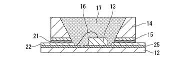
図3は、本発明の発光装置の第1実施形態を示す断面図である。図中、符号12は基板、13はLEDチップ、14はカップ部材、15は半田である。
Hereinafter, embodiments of the present invention will be described with reference to the drawings.
FIG. 3 is a cross-sectional view showing the first embodiment of the light-emitting device of the present invention. In the figure,
本実施形態では、基板12にLEDチップ13を実装し、そのLEDチップ13を囲むようにカップ部材14を半田15により基板12上に固定した構成になっている。このカップ部材14は、LEDチップ13を中心にして環状をなし、LEDチップ13から周囲に発した光を前方(図3においては上方)に向けて反射させる、斜めに広がった反射面を有している。
In this embodiment, the
半田固定は、金属同士の接続に用いられる接合方法で、非常に高い信頼性を有している。半田固定は、部材を固定する方法として一般的であるが、LEDチップ13を用いた照明器具におけるカップ部材14の固定では、配線との絶縁性確保の点から一般的には行われていない。しかし、絶縁性を保つ工夫をして半田固定を行えば、接着剤などと比較して、外部環境の影響をほとんど受けない、などの半田固定の長所を生かしたカップ部材14の固定を行うことができる。
Solder fixing is a joining method used for connecting metals, and has very high reliability. Solder fixing is a general method for fixing the member, but fixing of the
図4は、本発明の発光装置の第2実施形態を示す断面図である。本実施形態の発光装置は、図3に示す前記第1実施形態の発光装置と同様の構成要素を備え、さらに、カップ部材4の開口内に、LEDチップ13及び電気的接続用のワイヤ16を封止する透光性樹脂17を充填した構成になっている。
FIG. 4 is a cross-sectional view showing a second embodiment of the light-emitting device of the present invention. The light emitting device of this embodiment includes the same components as the light emitting device of the first embodiment shown in FIG. 3, and further, the
半田15により基板12上にカップ部材14を固定した場合、外力による変形も非常に小さいので、図4のようにカップ部材14内部に樹脂17が充填されている場合、LEDチップ13やワイヤ16への影響を小さくすることができる。
When the
本発明の発光装置において、カップ部材14の材質は特に限定するものではないが、LEDチップ13の光を反射させることを考えると金属製のものが望ましく、半田15の接合性も合わせて考えると、半田15がのりやすいようにニッケルめっき等をしてあることが望ましい。金属製ではなくても、たとえば樹脂製やセラミックス製のカップ部材に半田付けするための金属パットを取り付けた構造としてもよい。
In the light emitting device of the present invention, the material of the
また、カップ部材14の固定を半田によって行うことにより、他の電子製品と同時に、半田ペースト印刷・リフロー実装することが可能になり、カップ部材固定のための特別な工程・設備を省くことができる。このことにより、発光装置の生産性を向上させることができる。
Further, by fixing the
図5〜図7は、本発明において使用するカップ部材のさまざまな形状を示したものである。
図5は、基板18上に円環状(又は円筒状)のカップ部材19Aを半田で固定した場合を示す。
図6は、基板18上に四角環状(又は四角筒状)のカップ部材19Bを半田で固定した場合を示す。
図7は、基板18上に中空星形状のカップ部材19Cを半田で固定した場合を示す。
このようにカップ部材の形状は特に限定されるものではない。
5 to 7 show various shapes of the cup member used in the present invention.
FIG. 5 shows a case where an annular (or cylindrical)
FIG. 6 shows a case where a square annular (or square cylindrical)
FIG. 7 shows a case where a hollow star-shaped
Thus, the shape of the cup member is not particularly limited.
図8及び図9は、本発明の発光装置の第3実施形態を示す図である。本実施形態では、基板18上にカップ部材19Aを半田で固定する場合に、カップ部材19Aの下に電気配線20を通した構成になっている。この電気配線20の上には絶縁層22が形成されており、カップ部材14によりショートを起こさないようになっている。電気配線20が通る部分のカップ部材固定用の半田パターン21は、図9のように切れている。このような構造を採ることにより、カップ部材内部のLEDチップに電源を供給することができる。
8 and 9 are views showing a third embodiment of the light-emitting device of the present invention. In the present embodiment, when the
また、カップ固定用の半田パターン21は、電気配線パターンと同時に印刷やエッチングなどにより形成することができるので、カップ構造形成用の特別な設備や工程は不要である。このことにより、発光装置の生産性を上げることができる。
Further, since the
図10は、本発明の発光装置の第4実施形態を示す要部平面図である。本実施形態では、半田パターン21の2箇所に切欠23を入れた場合(a)、及び3箇所に切欠23を入れた場合(b)である。このように、半田パターン21において等角度に2つ又は3つの切欠23を入れることによって、カップ部材19Aを半田付けする際に、カップ部材19Aにかかる半田の表面張力が均等になり、カップ部材19Aを正確な場所に固定することができるようになる。
FIG. 10 is a plan view of a principal part showing a fourth embodiment of the light emitting device of the present invention. In this embodiment, it is a case where the
半田パターン21の形状は特に制限されるものではないが、前記と同じ理由により、切欠23により分割された個々の半田パターン21が同形となるような形状、例えば、円形とすることが望ましい。半田パターン21に入れる切欠23の数も特に限定されるものではない。
The shape of the
図11は、本発明の発光装置の第5実施形態を示す要部平面図である。本実施形態では、半田パターン21に半田溜24を設けている。半田溜24があると、余分な半田は半田溜24に逃げるので、カップ部材19Aを正確な場所に固定することができる。
FIG. 11 is a plan view of a principal part showing a fifth embodiment of the light-emitting device of the present invention. In the present embodiment, a
図12は、本発明の発光装置の第6実施形態を示す断面図である。本実施形態の発光装置は、基板12上に電気配線20となる回路パターン25を設け、この回路パターン25のうち、LEDチップ13実装位置とその近傍以外の回路パターン25上に絶縁層22を設け、この絶縁層22上にカップ部材固定用の半田パターン21を設け、この半田パターン21上にカップ部材14を半田15で固定し、このカップ部材14のカップ内に露出した一方の回路パターン25上にLEDチップ13を実装し、ワイヤ16で他方の回路パターン25と電気的に接続した構成になっている。
FIG. 12 is a cross-sectional view showing a sixth embodiment of the light-emitting device of the present invention. In the light emitting device of this embodiment, a
本実施形態では、カップ部材固定用の半田パターン21に切れ目が入らないため、より強固にカップ部材14を固定することができる。本実施形態の場合、カップ部材固定用の半田パターン21と回路パターン25は同一の層ではないため、印刷回数が増えるが、カップ固定用の半田パターン21を自由に設計でき、カップ部材14を強固に接合することができる。
In this embodiment, since no break is made in the
図13は、本発明の発光装置の第7実施形態を示す断面図である。本実施形態の発光装置は、図12に示す前記第6実施形態と同様の構成要素を備えて構成され、カップ部材14のカップ内側に向けて半田パターン21をはみ出させ、カップ部材14のカップ内側面に半田15を盛り上がらせたことを特徴としている。本実施形態によれば、カップ部材14の内側面に半田15により曲面が形成され、より効率的にLEDチップ13からの光を前面に反射させることができる。
FIG. 13 is a cross-sectional view showing a seventh embodiment of the light-emitting device of the present invention. The light emitting device of this embodiment is configured to include the same components as those of the sixth embodiment shown in FIG. 12, and the
図14は、本発明の発光装置の第8実施形態を示す断面図である。本実施形態の発光装置は、図12に示す前記第6実施形態とほぼ同様の構成要素を備えて構成され、カップ部材14に代えて、断面が円の線材26を曲げたものを用いたことを特徴としている。本実施形態では、半田パターン21、及び半田量を調節することにより、線材26の側面に曲面を形成することができ、より効率的にLEDチップ13からの光を前面に反射させることができる。また、カップ部材14に代えて線材26を用いていることにより、簡便かつ、低コストにカップ構造を形成することができる。
FIG. 14 is a cross-sectional view showing an eighth embodiment of the light-emitting device of the present invention. The light emitting device of the present embodiment is configured to include substantially the same components as those of the sixth embodiment shown in FIG. 12, and uses a
図15は、本発明の発光装置の第9実施形態を示す断面図である。本実施形態の発光装置は、図12に示す前記第6実施形態とほぼ同様の構成要素を備えて構成され、カップ部材14のカップに透光性樹脂17を充填した構成になっている。この樹脂17による封止構造は、前記いずれのカップ構造にも適用することができる。この透光性樹脂17には、光を拡散させる物や、波長を変換する蛍光体などが入っていても良い。
FIG. 15 is a sectional view showing a ninth embodiment of the light emitting device of the present invention. The light emitting device of the present embodiment is configured to include substantially the same components as those of the sixth embodiment shown in FIG. 12, and has a configuration in which the cup of the
12…基板、13…LEDチップ、14…カップ部材、15…半田、16…ワイヤ、17…透光性樹脂、18…基板、19A〜19C…カップ部材、20…電気配線、21…半田パターン、22…絶縁層、23…切欠、24…半田溜、25…回路パターン、26…線材。
DESCRIPTION OF
Claims (11)
Priority Applications (1)
| Application Number | Priority Date | Filing Date | Title |
|---|---|---|---|
| JP2007308814A JP5049757B2 (en) | 2007-11-29 | 2007-11-29 | Light emitting device |
Applications Claiming Priority (1)
| Application Number | Priority Date | Filing Date | Title |
|---|---|---|---|
| JP2007308814A JP5049757B2 (en) | 2007-11-29 | 2007-11-29 | Light emitting device |
Publications (2)
| Publication Number | Publication Date |
|---|---|
| JP2009135195A true JP2009135195A (en) | 2009-06-18 |
| JP5049757B2 JP5049757B2 (en) | 2012-10-17 |
Family
ID=40866842
Family Applications (1)
| Application Number | Title | Priority Date | Filing Date |
|---|---|---|---|
| JP2007308814A Expired - Fee Related JP5049757B2 (en) | 2007-11-29 | 2007-11-29 | Light emitting device |
Country Status (1)
| Country | Link |
|---|---|
| JP (1) | JP5049757B2 (en) |
Cited By (2)
| Publication number | Priority date | Publication date | Assignee | Title |
|---|---|---|---|---|
| KR20170000499A (en) * | 2015-06-24 | 2017-01-03 | 최종현 | Uv led package and the manufacturing method thereof |
| EP3382025A1 (en) | 2009-06-04 | 2018-10-03 | Toyota Jidosha Kabushiki Kaisha | Gene capable of increasing protein content in seed, and method for utilization thereof |
Citations (7)
| Publication number | Priority date | Publication date | Assignee | Title |
|---|---|---|---|---|
| JP2004039725A (en) * | 2002-07-01 | 2004-02-05 | Topcon Corp | Semiconductor laser device |
| JP2005129354A (en) * | 2003-10-23 | 2005-05-19 | Toshiba Lighting & Technology Corp | LED lighting device |
| JP2005183558A (en) * | 2003-12-18 | 2005-07-07 | Hitachi Ltd | Optical component mounting package and manufacturing method thereof |
| JP2006186297A (en) * | 2004-12-03 | 2006-07-13 | Toshiba Corp | Semiconductor light emitting device and manufacturing method thereof |
| JP2006332320A (en) * | 2005-05-26 | 2006-12-07 | Ngk Spark Plug Co Ltd | Wiring board for mounting light emitting element |
| JP2007227738A (en) * | 2006-02-24 | 2007-09-06 | Kyocera Corp | WIRING BOARD FOR LIGHT EMITTING ELEMENT AND LIGHT EMITTING DEVICE |
| JP2007281146A (en) * | 2006-04-05 | 2007-10-25 | Sharp Corp | Semiconductor light emitting device |
-
2007
- 2007-11-29 JP JP2007308814A patent/JP5049757B2/en not_active Expired - Fee Related
Patent Citations (7)
| Publication number | Priority date | Publication date | Assignee | Title |
|---|---|---|---|---|
| JP2004039725A (en) * | 2002-07-01 | 2004-02-05 | Topcon Corp | Semiconductor laser device |
| JP2005129354A (en) * | 2003-10-23 | 2005-05-19 | Toshiba Lighting & Technology Corp | LED lighting device |
| JP2005183558A (en) * | 2003-12-18 | 2005-07-07 | Hitachi Ltd | Optical component mounting package and manufacturing method thereof |
| JP2006186297A (en) * | 2004-12-03 | 2006-07-13 | Toshiba Corp | Semiconductor light emitting device and manufacturing method thereof |
| JP2006332320A (en) * | 2005-05-26 | 2006-12-07 | Ngk Spark Plug Co Ltd | Wiring board for mounting light emitting element |
| JP2007227738A (en) * | 2006-02-24 | 2007-09-06 | Kyocera Corp | WIRING BOARD FOR LIGHT EMITTING ELEMENT AND LIGHT EMITTING DEVICE |
| JP2007281146A (en) * | 2006-04-05 | 2007-10-25 | Sharp Corp | Semiconductor light emitting device |
Cited By (5)
| Publication number | Priority date | Publication date | Assignee | Title |
|---|---|---|---|---|
| EP3382025A1 (en) | 2009-06-04 | 2018-10-03 | Toyota Jidosha Kabushiki Kaisha | Gene capable of increasing protein content in seed, and method for utilization thereof |
| EP3382023A1 (en) | 2009-06-04 | 2018-10-03 | Toyota Jidosha Kabushiki Kaisha | Gene capable of increasing protein content in seed, and method for utilization thereof |
| EP3382024A1 (en) | 2009-06-04 | 2018-10-03 | Toyota Jidosha Kabushiki Kaisha | Gene capable of increasing protein content in seed, and method for utilization thereof |
| KR20170000499A (en) * | 2015-06-24 | 2017-01-03 | 최종현 | Uv led package and the manufacturing method thereof |
| KR101715789B1 (en) | 2015-06-24 | 2017-03-13 | 최종현 | Uv led package and the manufacturing method thereof |
Also Published As
| Publication number | Publication date |
|---|---|
| JP5049757B2 (en) | 2012-10-17 |
Similar Documents
| Publication | Publication Date | Title |
|---|---|---|
| JP3956965B2 (en) | Chip component type light emitting device and wiring board therefor | |
| US20110157897A1 (en) | Light Emitting Diode Module and Method for Making the Same | |
| US20130037845A1 (en) | Lead frame, and light emitting diode module having the same | |
| JP2008258617A (en) | LED package with metal PCB | |
| JP2015023219A (en) | LED light emitting device and manufacturing method of LED light emitting device | |
| JP5683922B2 (en) | Lamp, lighting device, and method of manufacturing lamp | |
| JP2020161697A (en) | Semiconductor light emitting device | |
| JP2010098181A (en) | Led light-emitting device | |
| JP5049757B2 (en) | Light emitting device | |
| JP2010045167A (en) | Semiconductor device | |
| JP6206266B2 (en) | LIGHT EMITTING MODULE FOR VEHICLE, LIGHTING DEVICE FOR VEHICLE, AND VEHICLE LIGHT | |
| JP4831958B2 (en) | Surface mount type LED | |
| JP5156138B2 (en) | Lamp and lighting device | |
| WO2010067701A1 (en) | Light-emitting device, light-emitting device module, and light-emitting device manufacturing method | |
| JP2006190888A (en) | Surface mount type LED | |
| JP5534423B2 (en) | Solid state light emitting device and lighting device | |
| CN101447534B (en) | Light-emitting diode and method of making the same | |
| JP4453004B2 (en) | Wiring board for mounting light-emitting elements | |
| JP2016039183A (en) | Method for manufacturing lighting apparatus and lighting apparatus | |
| JP2016018990A (en) | Package structure and method of manufacturing the same and mounting member | |
| JP6390899B2 (en) | VEHICLE LIGHTING DEVICE AND VEHICLE LIGHT | |
| JP2010287749A (en) | Luminescent body and lighting fixture | |
| JP2007201104A (en) | Light emitting device | |
| JP6650480B2 (en) | Light emitting device module | |
| KR100583161B1 (en) | Light emitting diode package |
Legal Events
| Date | Code | Title | Description |
|---|---|---|---|
| A621 | Written request for application examination |
Free format text: JAPANESE INTERMEDIATE CODE: A621 Effective date: 20100607 |
|
| A977 | Report on retrieval |
Free format text: JAPANESE INTERMEDIATE CODE: A971007 Effective date: 20120329 |
|
| A131 | Notification of reasons for refusal |
Free format text: JAPANESE INTERMEDIATE CODE: A131 Effective date: 20120403 |
|
| A521 | Request for written amendment filed |
Free format text: JAPANESE INTERMEDIATE CODE: A523 Effective date: 20120604 |
|
| TRDD | Decision of grant or rejection written | ||
| A01 | Written decision to grant a patent or to grant a registration (utility model) |
Free format text: JAPANESE INTERMEDIATE CODE: A01 Effective date: 20120626 |
|
| A01 | Written decision to grant a patent or to grant a registration (utility model) |
Free format text: JAPANESE INTERMEDIATE CODE: A01 |
|
| A61 | First payment of annual fees (during grant procedure) |
Free format text: JAPANESE INTERMEDIATE CODE: A61 Effective date: 20120723 |
|
| FPAY | Renewal fee payment (event date is renewal date of database) |
Free format text: PAYMENT UNTIL: 20150727 Year of fee payment: 3 |
|
| R250 | Receipt of annual fees |
Free format text: JAPANESE INTERMEDIATE CODE: R250 |
|
| R250 | Receipt of annual fees |
Free format text: JAPANESE INTERMEDIATE CODE: R250 |
|
| LAPS | Cancellation because of no payment of annual fees |