JP2008286963A - Display device and driving method of display device - Google Patents
Display device and driving method of display device Download PDFInfo
- Publication number
- JP2008286963A JP2008286963A JP2007131210A JP2007131210A JP2008286963A JP 2008286963 A JP2008286963 A JP 2008286963A JP 2007131210 A JP2007131210 A JP 2007131210A JP 2007131210 A JP2007131210 A JP 2007131210A JP 2008286963 A JP2008286963 A JP 2008286963A
- Authority
- JP
- Japan
- Prior art keywords
- signal
- amplitude
- voltage system
- display device
- transistor
- Prior art date
- Legal status (The legal status is an assumption and is not a legal conclusion. Google has not performed a legal analysis and makes no representation as to the accuracy of the status listed.)
- Pending
Links
Images


Landscapes
- Control Of Indicators Other Than Cathode Ray Tubes (AREA)
- Control Of El Displays (AREA)
- Shift Register Type Memory (AREA)
Abstract
【課題】本発明は、表示装置及び表示装置の駆動方法に関し、例えばポリシリコンTFTを用いた有機EL素子によるアクティブマトリックス型のディスプレイ装置に適用して、消費電力、周辺回路の面積の増大を有効に回避して、従来に比して走査線に出力する駆動信号の精度を向上する。
【解決手段】本発明は、画素の駆動に適した第3の電圧系の振幅より小さな第2の電圧系の振幅で選択信号を生成した後、第3の電圧系の振幅に変換し、この第3の電圧系の振幅による選択信号を基準にして第3の電圧系の振幅による垂直イネーブル信号を処理して駆動信号を生成する。
【選択図】 図1The present invention relates to a display device and a driving method of the display device, and is applied to, for example, an active matrix display device using an organic EL element using a polysilicon TFT to effectively increase power consumption and area of a peripheral circuit. Therefore, the accuracy of the drive signal output to the scanning line is improved as compared with the conventional case.
The present invention generates a selection signal with an amplitude of a second voltage system smaller than an amplitude of a third voltage system suitable for driving a pixel, and then converts the selection signal into an amplitude of a third voltage system. Based on the selection signal based on the amplitude of the third voltage system, the vertical enable signal based on the amplitude of the third voltage system is processed to generate a drive signal.
[Selection] Figure 1
Description
本発明は、表示装置及び表示装置の駆動方法に関し、例えばポリシリコンTFT(Thin Film Transistor)を用いた有機EL(Electro Luminescence)素子によるアクティブマトリックス型のディスプレイ装置に適用することができる。本発明は、画素の駆動に適した第3の電圧系の振幅より小さな第2の電圧系の振幅で選択信号を生成した後、第3の電圧系の振幅に変換し、この第3の電圧系の振幅による選択信号を基準にして第3の電圧系の振幅による垂直イネーブル信号を処理して駆動信号を生成することにより、消費電力、周辺回路の面積の増大を有効に回避して、従来に比して走査線に出力する駆動信号の精度を向上する。 The present invention relates to a display device and a display device driving method, and can be applied to an active matrix display device using an organic EL (Electro Luminescence) element using, for example, a polysilicon TFT (Thin Film Transistor). In the present invention, after the selection signal is generated with the amplitude of the second voltage system smaller than the amplitude of the third voltage system suitable for driving the pixel, the selection signal is converted into the amplitude of the third voltage system, and this third voltage is converted. By generating a drive signal by processing the vertical enable signal based on the amplitude of the third voltage system on the basis of the selection signal based on the system amplitude, it is possible to effectively avoid an increase in power consumption and area of the peripheral circuit. Compared with the above, the accuracy of the drive signal output to the scanning line is improved.
従来、ポリシリコンを用いたアクティブマトリックス型のディスプレイ装置では、ガラス基板等による絶縁基板上にマトリックス状に画素を配置して表示部が形成され、この絶縁基板上、表示部の周囲に、表示部を駆動する垂直駆動回路、水平駆動回路等が設けられる。 2. Description of the Related Art Conventionally, in an active matrix display device using polysilicon, a display unit is formed by arranging pixels in a matrix on an insulating substrate such as a glass substrate, and the display unit is formed around the display unit on the insulating substrate. Are provided with a vertical drive circuit, a horizontal drive circuit, and the like.
ここで図15は、この種のディスプレイ装置を示すブロック図である。このディスプレイ装置1において、表示部2は、例えば有機EL素子による電流駆動型の発光素子を有する画素3がマトリックス状に配置されて形成される。表示部2は、このマトリックス状に配置した画素3に対して、走査線VSCAN1(1)〜VSCAN1(4)がライン単位で水平方向に設けられ、また走査線VSCAN1(1)〜VSCAN1(4)と直交するように信号線SIG(1)〜SIG(3)が列毎に設けられる。なおこの図15では、3×4個の画素により表示部2を形成した場合を示す。また実際のディスプレイ装置では、各画素3の構成に応じて、1つの画素3に複数の走査線が設けられるが、この図15の例では、1つの画素3に1つの走査線VSCAN1(1)〜VSCAN1(4)が設けられている場合を示す。
FIG. 15 is a block diagram showing this type of display device. In the
Hスキャン回路4は、水平駆動回路であり、各画素3の階調を示す画像データD1を入力し、この画像データD1を所定のクロックHCKにより順次ラッチして各信号線SIG(1)〜SIG(3)に振り分ける。さらにHスキャン回路4は、この振り分けた画像データD1をアナログディジタル変換処理し、対応する信号線SIG(1)〜SIG(3)に接続された画素3の階調を時分割により示す駆動信号を各信号線SIG(1)〜SIG(3)に出力する。
The
Vスキャン回路5は、垂直駆動回路に設けられ、各画素3の動作を制御する駆動信号S2(1)〜S2(4)を生成して走査線VSCAN1(1)〜VSCAN1(4)に出力する。より具体的に、Vスキャン回路5は、図16に示すように、所定の基準パルスである垂直同期信号に同期した垂直スタートパルスVST(図16(A))を、垂直クロックVCK(図16(B))により順次転送し、走査線VSCAN1(1)〜VSCAN1(4)毎に、走査線VSCAN1(1)〜VSCAN1(4)を順次選択する選択信号S1(1)〜S1(4)(図16(D1)〜(D4))を生成する。Vスキャン回路5は、この選択信号S1(1)〜S1(4)を基準にして垂直イネーブル信号VEN(図16(C))を処理することにより、走査線VSCAN1(1)〜VSCAN1(4)毎に、各走査線VSCAN1(1)〜VSCAN1(4)に接続された画素3の動作を制御する駆動信号S2(1)〜S2(4)(図16(E1)〜(E4))を生成する。なおここで垂直イネーブル信号VEN(図16(C))は、各駆動信号S2(1)〜S2(4)において信号レベルの切り換わるタイミングを設定する基準信号であり、この図16の例では垂直イネーブル信号VEN(図16(C))をそれぞれ選択信号S1(1)〜S1(4)により選択して駆動信号S2(1)〜S2(4)(図16(E1)〜(E4))を生成する。
The
ここでこの種のディスプレイ装置1では、垂直スタートパルスVST、垂直クロックVCK、垂直イネーブル信号VENが3〔V〕以下の振幅でVスキャン回路5に入力される。これに対してポリシリコンの回路は、数V〜10数Vの駆動電圧が必要であり、有機EL素子の駆動には、さらに大きな振幅が必要になる。そこでVスキャン回路5は、垂直スタートパルスVST、垂直クロックVCK、垂直イネーブル信号VENから各走査線VSCAN1(1)〜VSCAN1(4)の駆動信号S2(1)〜S2(4)(図16(E1)〜(E4))を生成する際に、レベル変換回路を用いて、これら垂直スタートパルスVST、垂直クロックVCK、垂直イネーブル信号VEN等の振幅、駆動信号S2(1)〜S2(4)の振幅を補正する。
In this type of
図17は、Vスキャン回路5の具体的構成を示すブロック図である。このVスキャン回路5は、例えばHレベル及びLレベルが3〔V〕及び0〔V〕の振幅で垂直スタートパルスVST、垂直クロックVCK、垂直イネーブル信号VENを入力する。なお以下において、このVスキャン回路5の入力信号の振幅を第1の電圧系の振幅と呼び、符号Iにより示す。
FIG. 17 is a block diagram showing a specific configuration of the
Vスキャン回路5において、レベル変換回路(L/S)6〜8は、これら垂直スタートパルスVST、垂直クロックVCK、垂直イネーブル信号VENの振幅を、ポリシリコンの回路の駆動に適し、かつ有機EL素子の駆動に適した振幅より小さな、例えばHレベル及びLレベルが10〔V〕及び0〔V〕の振幅に補正する。なお以下において、このポリシリコンの回路の駆動に適し、かつ有機EL素子の駆動に適した振幅より小さな振幅を第2の電圧系の振幅と呼び、符号IIにより示す。
In the
シフトレジスタ(S/R)10(1)〜10(4)は、レベル変換回路6から出力される垂直スタートパルスVSTを、レベル変換回路7から出力される垂直クロックVCKにより順次転送し、Hレベル及びLレベルが10〔V〕及び0〔V〕の選択信号S1(1)〜S1(4)を生成する。
The shift registers (S / R) 10 (1) to 10 (4) sequentially transfer the vertical start pulse VST output from the
論理回路11(1)〜11(4)は、この選択信号S1(1)〜S1(4)を基準にして垂直イネーブル信号VEN(図16(C))を論理演算処理することにより、走査線VSCAN1(1)〜VSCAN1(4)毎に、Hレベル及びLレベルが10〔V〕及び0〔V〕の駆動信号S2(1)〜S2(4)を生成する。より具体的に、論理回路11(1)〜11(4)は、図16について上述した例ではアンド回路により構成され、レベル変換回路7から出力される垂直イネーブル信号VENと、各選択信号S1(1)〜S1(4)との論理積をそれぞれ計算して駆動信号S2(1)〜S2(4)を生成する。
The logic circuits 11 (1) to 11 (4) perform a logical operation process on the vertical enable signal VEN (FIG. 16C) based on the selection signals S1 (1) to S1 (4), thereby scanning lines. For each of VSCAN1 (1) to VSCAN1 (4), drive signals S2 (1) to S2 (4) having H level and L level of 10 [V] and 0 [V] are generated. More specifically, the logic circuits 11 (1) to 11 (4) are configured by AND circuits in the example described above with reference to FIG. 16, and the vertical enable signal VEN output from the
なお駆動信号には、近接する走査線に出力する駆動信号等に応じて波形を切り換える場合、インターレース方式により奇数フィールドと偶数フィールドとで波形を切り換える場合等もあり、このような場合、論理回路11(1)〜11(4)は、さらに複雑な論理演算処理を実行して駆動信号S2(1)〜S2(4)を生成する。 The drive signal may be switched in accordance with a drive signal or the like output to an adjacent scanning line, or may be switched between an odd field and an even field by an interlace method. In such a case, the logic circuit 11 (1) to 11 (4) execute further complicated logical operation processing to generate drive signals S2 (1) to S2 (4).
レベル変換回路(L/S)12(1)〜12(4)は、論理回路11(1)〜11(4)から出力される駆動信号S2(1)〜S2(4)の振幅を、有機EL素子の駆動に適した例えばHレベル及びLレベルが15〔V〕及び−5〔V〕の振幅に変換して出力する。なお以下において、この有機EL素子の駆動に適した振幅を第3の電圧系の振幅と呼び、符号III により示す。バッファ回路13(1)〜13(4)は、レベル変換回路(L/S)12(1)〜12(4)から出力される駆動信号S2(1)〜S2(4)により各走査線VSCAN1(1)〜VSCAN1(4)を駆動する。 The level conversion circuits (L / S) 12 (1) to 12 (4) use the amplitudes of the drive signals S2 (1) to S2 (4) output from the logic circuits 11 (1) to 11 (4) as an organic signal. For example, H level and L level suitable for driving the EL element are converted into amplitudes of 15 [V] and −5 [V] and output. In the following, the amplitude suitable for driving the organic EL element is referred to as the amplitude of the third voltage system, and is denoted by reference numeral III. The buffer circuits 13 (1) to 13 (4) are connected to the scanning lines VSCAN 1 by the drive signals S 2 (1) to S 2 (4) output from the level conversion circuits (L / S) 12 (1) to 12 (4). (1) to VSCAN1 (4) are driven.
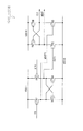
図18は、レベル変換回路6〜8の構成を示す接続図である。レベル変換回路6〜8は、いわゆるカレントミラー型のレベル変換回路であり、第2の電圧系IIのHレベルに対応する正側電源VDDIIにそれぞれドレインを接続したPチャンネル型のトランジスタTR1及びTR2によるカレントミラー回路が設けられ、これらトランジスタTR1及びTR2のソースに、それぞれNチャンネル型のトランジスタTR3及びTR4のドレインが接続される。これらトランジスタTR3及びTR4は、それぞれゲートが正側電源VDDIIに接続され、図19(A)に示すように、第1の電圧系Iの振幅による入力信号IN、入力信号INの反転信号XINがソースに入力される。なおトランジスタTR4のソースは、反転信号XINの入力に代えて、一定電圧の基準電圧REFに設定される場合もあり、この基準電圧REFは、入力信号INのHレベル及びLレベルの略平均の電圧に設定される。
FIG. 18 is a connection diagram showing the configuration of the level conversion circuits 6-8. The
これによりレベル変換回路6〜8は、第1の電圧系Iにより入力される垂直スタートパルスVST、垂直クロックVCK、又は垂直イネーブル信号VENによる入力信号INに応じてトランジスタTR3、TR4が相補的にオンオフ動作し、トランジスタTR3、TR4のドレイン電圧を第2の電圧系IIの振幅で変化させる。レベル変換回路6〜8は、トランジスタTR3のドレイン電圧をバッファ回路15を介して出力し、これにより第1の電圧系Iの振幅による入力信号INを第2の電圧系IIの振幅により出力する。なおこの図19において、電圧VSSIIは、第2の電圧系IIのLレベルに対応する負側電源の電圧であり、図18の例ではグランドレベルである。
As a result, in the
なおレベル変換回路6〜8には、種々の回路構成を適用することができる。図20は、図18との対比により他の回路構成によるレベル変換回路を示す接続図である。この図20のレベル変換回路17は、図18のレベル変換回路と同様のカレントミラー型のレベル変換回路であり、正側電源VDDIIにそれぞれドレインを接続したPチャンネル型のトランジスタTR1及びTR2によるカレントミラー回路が設けられ、これらトランジスタTR1及びTR2のソースに、それぞれNチャンネル型のトランジスタTR3及びTR4のドレインが接続される。ここでこれらトランジスタTR3及びTR4は、それぞれ第1の電圧系Iの振幅による入力信号IN、入力信号INの反転信号XINがソースに入力され、トランジスタTR3のドレイン電圧がバッファ回路15を介して出力される。
Various circuit configurations can be applied to the
レベル変換回路17は、それぞれソース接地型のトランジスタTR5及びTR6のゲートに反転信号XIN及び入力信号INが入力されると共に、これらトランジスタTR5及びTR6のドレインが、トランジスタTR3及びTR4のゲートに接続され、これによりトランジスタTR5及びTR6を介して反転信号XIN及び入力信号INがトランジスタTR3及びTR4に入力される。なおこれらトランジスタTR5及びTR6は、ゲートを接地したトランジスタTR7及びTR8をそれぞれ介してドレインが負側電源VDDII(この図20ではグランドレベル)に接続される。
In the
またトランジスタTR3及びTR4とゲート及びソースを共通に接続したトランジスタTR9、TR10のドレインが、これらトランジスタTR5及びTR6のドレインに接続される。これによりこのレベル変換回路17は、十分な帰還利得によりトランジスタTR3、TR4をオンオフ動作させて、第1の電圧系Iによる入力信号INを第2の電圧系IIにより出力する。なおこの図20のレベル変換回路17のタイムチャートは、図18のレベル変換回路のタイムチャートと同一に、図19で表される。
The drains of the transistors TR9 and TR10, whose gates and sources are connected in common with the transistors TR3 and TR4, are connected to the drains of the transistors TR5 and TR6. As a result, the
これに対して第2の電圧系IIを第3の電圧系III に変換するレベル変換回路12(1)〜12(4)は、走査線VSCAN1(1)〜VSCAN1(4)毎に設けられることから、Vスキャン回路5に設けられる数が多くなる。従って図18、図20等により示すカレントミラー型のレベル変換回路を適用したのでは、ディスプレイ装置の消費電力が著しく増大することになる。
On the other hand, level conversion circuits 12 (1) to 12 (4) for converting the second voltage system II to the third voltage system III are provided for each of the scanning lines VSCAN1 (1) to VSCAN1 (4). Therefore, the number provided in the
そこで例えば図21に示すように、これらのレベル変換回路12(1)〜12(4)には、いわゆるラッチ型のレベル変換回路が適用される。すなわちこれらのレベル変換回路12(1)〜12(4)は、第2の電圧系IIのHレベルに対応する正側電源VDDIIにそれぞれドレインを接続したトランジスタTR1及びTR2のゲートに、図22((A))により示す第2の電圧系IIの振幅による入力信号IN及び入力信号INの反転信号XINを入力する。ここでこれらトランジスタTR1及びTR2は、それぞれトランジスタTR3及びTR4を介して、第3の電圧系III のLレベルに対応する負側電源VSSIII にソースが接続され、これらトランジスタTR3及びTR4は、相互にゲート及びドレインが接続される。これによりレベル変換回路12(1)〜12(4)は、図22(B)により示すように、第2の電圧系IIによる入力信号IN及び反転入力信号XINに応じて相補的にオンオフ動作し、第2の電圧系IIのHレベルと第3の電圧系III のLレベルとの間でトランジスタTR3及びTR4のドレイン電圧を切り換え、このドレイン電圧による出力信号OUT1、XOUT1をトランジスタTR5及びTR6に出力する。 Therefore, for example, as shown in FIG. 21, a so-called latch type level conversion circuit is applied to the level conversion circuits 12 (1) to 12 (4). That is, these level conversion circuits 12 (1) to 12 (4) are connected to the gates of the transistors TR1 and TR2 whose drains are respectively connected to the positive power supply VDDII corresponding to the H level of the second voltage system II. The input signal IN and the inverted signal XIN of the input signal IN with the amplitude of the second voltage system II indicated by (A)) are input. Here, the sources of these transistors TR1 and TR2 are connected to the negative power source VSSIII corresponding to the L level of the third voltage system III via the transistors TR3 and TR4, respectively, and these transistors TR3 and TR4 are mutually gated. And the drain are connected. As a result, the level conversion circuits 12 (1) to 12 (4) are complementarily turned on and off according to the input signal IN and the inverted input signal XIN by the second voltage system II, as shown in FIG. The drain voltages of the transistors TR3 and TR4 are switched between the H level of the second voltage system II and the L level of the third voltage system III, and output signals OUT1 and XOUT1 based on the drain voltages are output to the transistors TR5 and TR6. To do.
トランジスタTR5及びTR6は、第3の電圧系III の負側電源VSSIII にソースが接続され、ゲートにそれぞれ出力信号OUT1、XOUT1を入力する。これらトランジスタTR5及びTR6は、それぞれトランジスタTR7及びTR8を介して、第3の電圧系III のHレベルに対応する正側電源VDDIII にゲートが接続され、これらトランジスタTR7及びTR8は、相互にゲート及びドレインが接続される。これによりレベル変換回路12(1)〜12(4)は、図22(C)により示すように、第2の電圧系IIの振幅による入力信号IN及び反転入力信号XINに応じて、第3の電圧系III のHレベルとLレベルとの間でトランジスタTR5及びTR6のドレイン電圧を切り換え、このドレイン電圧による出力信号OUT2、XOUT2を出力する。
The sources of the transistors TR5 and TR6 are connected to the negative power source VSSIII of the third voltage system III, and the output signals OUT1 and XOUT1 are input to the gates, respectively. The gates of these transistors TR5 and TR6 are connected to the positive power supply VDDIII corresponding to the H level of the third voltage system III via the transistors TR7 and TR8, respectively. Is connected. As a result, the level conversion circuits 12 (1) to 12 (4) allow the
この種のVスキャン回路では、図17との対比により図23に示すように、垂直クロックVCKの振幅を補正するレベル変換回路7を省略する構成もあり、この構成のVスキャン回路18では、シフトレジスタ10(1)〜10(4)に代えて、図24に示すSRラッチ回路構成のシフトレジスタ19(1)〜19(4)により垂直スタートパルスVSTを順次転送する。
In this type of V scan circuit, as shown in FIG. 23 in comparison with FIG. 17, there is also a configuration in which the
すなわちシフトレジスタ19(1)〜19(4)は(図24)、バッファ回路21を介して出力信号OUT(S2(1)〜S2(4))をそれぞれ出力するようにして、シフトレジスタ19(1)〜19(4)の入力信号IN(図25(B))とバッファ回路21の入力信号との論理和信号がオア回路22で生成される。シフトレジスタ19(1)〜19(4)は、インバータ23、ソース接地型のトランジスタTR1を介して、この論理和信号がトランジスタTR2のソースに入力される。ここでこのトランジスタTR2は、第2の電圧系IIの正側電源VDDIIにドレインが接続され、この正側電源VDDIIにドレインを接続して論理和信号をゲートに入力するトランジスタTR3のソースがゲートに接続される。またトランジスタTR2は、論理和信号をゲートに入力して垂直クロックVCKの反転信号XVCK(図25(A))をソースに入力するトランジスタTR4のドレインがゲートに接続され、ダイオード接続のトランジスタTR5を介して垂直クロックVCKがソースに入力される。
That is, the shift registers 19 (1) to 19 (4) (FIG. 24) output the output signals OUT (S 2 (1) to S 2 (4)) via the
シフトレジスタ19(1)〜19(4)は、このダイオード接続のトランジスタTR5に対して、トランジスタTR6がカレントミラー回路構成により接続され、このトランジスタTR6のソースにクロックVCKの反転信号XVCKが入力される。またこのトランジスタTR6のドレインがトランジスタTR7のソースに接続される。またこのトランジスタTR7のゲートに、トランジスタTR2と同様にトランジスタTR8を介して論理和信号が入力され、トランジスタTR2とは逆に、トランジスタTR9を介してクロックVCKが入力される。 In the shift registers 19 (1) to 19 (4), the transistor TR6 is connected to the diode-connected transistor TR5 in a current mirror circuit configuration, and the inverted signal XVCK of the clock VCK is input to the source of the transistor TR6. . The drain of the transistor TR6 is connected to the source of the transistor TR7. Similarly to the transistor TR2, a logical sum signal is input to the gate of the transistor TR7 via the transistor TR8. On the contrary to the transistor TR2, the clock VCK is input via the transistor TR9.
シフトレジスタ19(1)〜19(4)は、このトランジスタTR7のソースがトランジスタTR10により第2の電圧系IIの電源電圧VDDIIにプルアップされ、このトランジスタTR7のソース電圧が、インバータ24、バッファ回路21を介して出力される。これによりシフトレジスタ19(1)〜19(4)は、図25(A)〜(C)に示すように、第2の電圧系による垂直スタートパルスVSTを、第1の電圧系Iによる垂直クロックVCK、垂直クロックVCKの反転信号XVCKにより順次転送して第2の電圧系の振幅により出力する。なお図17及び図23との対比により図26に示すように、シフトレジスタに代えて、デコーダ26により選択信号S1(1)〜S1(4)を生成する場合もある。
In the shift registers 19 (1) to 19 (4), the source of the transistor TR7 is pulled up to the power supply voltage VDDII of the second voltage system II by the transistor TR10, and the source voltage of the transistor TR7 is supplied to the
この種の有機EL素子を用いたディスプレイ装置に関しては、例えばUSP5,684,365、特開平8−234683号公報等に種々の工夫が提案されている。 With regard to a display device using this type of organic EL element, various devices have been proposed in, for example, USP 5,684,365, Japanese Patent Laid-Open No. 8-234683, and the like.
ところでこれら図17、図23、図26によるVスキャン回路では、走査線VSCAN1(1)〜VSCAN1(4)毎に、第2の電圧系IIの振幅を第3の電圧系III の振幅に変換するレベル変換回路12(1)〜12(4)が設けられる。これに対してポリシリコン回路によるラッチ型のレベル変換回路では、回路間で遅延時間がばらつき、これにより回路間でタイミングのばらつきが大きい欠点がある。これによりこれら図17、図23、図26によるVスキャン回路では、各走査線VSCAN1(1)〜VSCAN1(4)の駆動信号S1(1)〜S1(4)間でタイミングがばらつき、このタイミングのばらつきが表示画像に種々に影響を与える問題がある。 By the way, in the V scan circuits shown in FIGS. 17, 23 and 26, the amplitude of the second voltage system II is converted into the amplitude of the third voltage system III for each of the scanning lines VSCAN1 (1) to VSCAN1 (4). Level conversion circuits 12 (1) to 12 (4) are provided. On the other hand, the latch type level conversion circuit using the polysilicon circuit has a drawback that the delay time varies among the circuits, and thus the timing varies greatly among the circuits. As a result, in the V scan circuits according to FIGS. 17, 23, and 26, the timing varies between the drive signals S1 (1) to S1 (4) of the scan lines VSCAN1 (1) to VSCAN1 (4). There is a problem that variations affect the displayed image in various ways.
この問題を解決する1つの方法として、図21について上述したラッチ型のレベル変換回路12(1)〜12(4)に代えて、回路間でタイミングのばらつきが小さい図18、図20について上述したカレントミラー型のレベル変換回路を適用することが考えられる。しかしながらこの方法では、消費電力が著しく増大する欠点がある。 As one method for solving this problem, instead of the latch-type level conversion circuits 12 (1) to 12 (4) described above with reference to FIG. 21, the timing variation between circuits is small as described above with reference to FIGS. It is conceivable to apply a current mirror type level conversion circuit. However, this method has a drawback that the power consumption is remarkably increased.
また周辺回路を含めた全体を第3の電圧系III で動作させる方法も考えられるが、この方法の場合も消費電力が著しく増大する。またこの方法では、トランジスタの大きさが大きくなり、周辺回路の面積が増加する欠点もある。
本発明は以上の点を考慮してなされたもので、消費電力、周辺回路の面積の増大を有効に回避して、従来に比して走査線に出力する駆動信号の精度を向上させることができる表示装置及び表示装置の駆動方法を提案しようとするものである。 The present invention has been made in consideration of the above points, and can effectively avoid an increase in power consumption and the area of peripheral circuits, and can improve the accuracy of a drive signal output to a scanning line as compared with the prior art. The present invention is intended to propose a display device that can be used and a method for driving the display device.
上記の課題を解決するため請求項1の発明は、画素をマトリックス状に配置して形成された表示部の走査線に、垂直駆動回路から駆動信号を出力して前記画素を駆動することにより、前記表示部で所望の画像を表示する表示装置に適用して、前記垂直駆動回路は、基準パルスを処理して、前記画素の駆動に適した第3の電圧系の振幅より小さな第2の電圧系の振幅により、前記走査線毎に、前記走査線を順次選択する選択信号を生成する選択信号生成回路と、前記走査線毎に、前記第2の電圧系の振幅による前記選択信号を前記第3の電圧系の振幅に変換する走査線毎のレベル変換回路と、前記走査線毎に、前記走査線毎のレベル変換回路の出力信号をそれぞれ基準にして、前記駆動信号において信号レベルの切り換わるタイミングを設定する前記第3の電圧系の振幅による垂直イネーブル信号を処理することにより、前記第3の電圧系により前記駆動信号を生成する走査線毎の駆動信号生成回路とを備えるようにする。
In order to solve the above-mentioned problem, the invention of
また請求項8の発明は、画素をマトリックス状に配置して形成された表示部の走査線に、垂直駆動回路から駆動信号を出力して前記画素を駆動することにより、前記表示部で所望の画像を表示する表示装置の駆動方法に適用して、基準パルスを処理して、前記画素の駆動に適した第3の電圧系の振幅より小さな第2の電圧系の振幅により、前記走査線毎に、前記走査線を順次選択する選択信号を生成する選択信号生成のステップと、前記走査線毎に、前記第2の電圧系の振幅による前記選択信号を前記第3の電圧系の振幅に変換する走査線毎のレベル変換のステップと、前記走査線毎に、前記走査線毎のレベル変換のステップによる出力信号をそれぞれ基準にして、前記駆動信号において信号レベルの切り換わるタイミングを設定する前記第3の電圧系の振幅による垂直イネーブル信号を処理することにより、前記第3の電圧系により前記駆動信号を生成する走査線毎の駆動信号生成のステップとを有するようにする。 According to an eighth aspect of the present invention, a desired signal is output from the display unit by driving the pixel by outputting a drive signal from a vertical drive circuit to a scanning line of the display unit formed by arranging pixels in a matrix. Applying to the driving method of the display device for displaying an image, the reference pulse is processed, and the amplitude of the second voltage system smaller than the amplitude of the third voltage system suitable for driving the pixel is used for each scanning line. In addition, a selection signal generation step for generating a selection signal for sequentially selecting the scanning lines, and the selection signal based on the amplitude of the second voltage system is converted into the amplitude of the third voltage system for each scanning line. The timing for switching the signal level in the drive signal is set for each scanning line with reference to the output signal from the level conversion step for each scanning line and the level conversion step for each scanning line. By by the amplitude of the voltage system processes the vertical enable signal, to have a driving signal generation step in each scan line to generate the drive signal by said third voltage system.
請求項1又は請求項8の構成によれば、駆動信号において信号レベルの切り換わるタイミングを設定する垂直イネーブル信号を第3の電圧系の振幅で各走査線に対して共通に供給することができる。従って走査線毎に、レベル変換回路を設ける場合の、走査線間の駆動信号のタイミングのばらつきを防止することができ、これにより従来に比して走査線に出力する駆動信号の精度を向上させることができる。また基準パルスにあっては、第2の電圧系の振幅で選択信号を生成し、その後、第3の電圧系の振幅に変換することから、全体を第3の電圧系の振幅で処理する場合のような消費電力、周辺回路の面積の増大を有効に回避することができる。 According to the configuration of the first or eighth aspect, the vertical enable signal for setting the timing of switching the signal level in the drive signal can be commonly supplied to each scanning line with the amplitude of the third voltage system. . Therefore, when the level conversion circuit is provided for each scanning line, it is possible to prevent the variation in the timing of the driving signal between the scanning lines, thereby improving the accuracy of the driving signal output to the scanning line as compared with the conventional case. be able to. In the case of the reference pulse, since the selection signal is generated with the amplitude of the second voltage system and then converted into the amplitude of the third voltage system, the whole is processed with the amplitude of the third voltage system. Such an increase in power consumption and the area of the peripheral circuit can be effectively avoided.
本発明によれば、消費電力、周辺回路の面積の増大を有効に回避して、従来に比して走査線に出力する駆動信号の精度を向上させることができる。 According to the present invention, it is possible to effectively avoid an increase in power consumption and the area of the peripheral circuit, and to improve the accuracy of the drive signal output to the scanning line as compared with the prior art.
以下、適宜図面を参照しながら本発明の実施例を詳述する。 Hereinafter, embodiments of the present invention will be described in detail with reference to the drawings as appropriate.
(1)実施例の構成
図2は、本発明の実施例1のディスプレイ装置に適用される画素の構成を示す接続図である。この実施例のディスプレイ装置は、透明絶縁基板であるガラス基板上に、ポリシリコンTFT等により表示部、水平駆動回路、垂直駆動回路が一体に形成される。この実施例のディスプレイ装置は、画素33をマトリックス状に配置して表示部が形成され、この表示部の周囲、ガラス基板上に水平駆動回路及び垂直駆動回路が設けられる。
(1) Configuration of Embodiment FIG. 2 is a connection diagram illustrating a configuration of a pixel applied to the display device of
各画素33は、電流駆動型の発光素子である有機EL素子34と、この有機EL素子34を駆動する各画素33の駆動回路(以下、画素回路と呼ぶ)とで形成される。
Each pixel 33 is formed by an
画素33は、有機EL素子34のカソードが所定の負側電源VSS2に接続される。画素回路は、トランジスタTR3のソースに有機EL素子34のアノードが接続され、走査線VSCAN2により供給される駆動信号S22によりオンオフ動作するPチャンネル型のトランジスタTR2を介して、このトランジスタTR3のドレインが正側電源VDD1に接続される。これにより画素33は、この駆動信号S22により有機EL素子34の発光、非発光を制御して、トランジスタTR3のゲートソース間電圧に応じた電流で有機EL素子34を駆動する。
In the pixel 33, the cathode of the
画素回路は、このトランジスタTR3のゲート及びソースに、信号レベル保持用コンデンサCsの両端が接続される。さらに画素回路は、走査線VSCAN1により供給される駆動信号S21によりオンオフ動作するトランジスタTR1を介して、このトランジスタTR3のゲートが信号線SIGに接続される。これにより画素回路は、駆動信号S21によりトランジスタTR1をオンオフ制御して信号レベル保持用コンデンサCsの一端の電圧を信号線SIGの電位Vsigに設定し、有機EL素子34の発光輝度を設定する。
In the pixel circuit, both ends of a signal level holding capacitor Cs are connected to the gate and source of the transistor TR3. Further, in the pixel circuit, the gate of the transistor TR3 is connected to the signal line SIG via the transistor TR1 that is turned on and off by the drive signal S21 supplied by the scanning line VSCAN1. As a result, the pixel circuit controls the transistor TR1 to be turned on / off by the drive signal S21, sets the voltage at one end of the signal level holding capacitor Cs to the potential Vsig of the signal line SIG, and sets the emission luminance of the
さらに画素回路は、走査線VSCAN4により供給される駆動信号S24によりオンオフ動作するトランジスタTR5を介して、トランジスタTR3のゲートが所定の固定電位Vofsに接続され、また走査線VSCAN3により供給される駆動信号S23によりオンオフ動作するトランジスタTR4を介して、このトランジスタTR3のソースが所定の固定電位Viniに接続される。画素回路は、走査線VSCAN1〜VSCAN4によるこれらトランジスタTR1、TR2、TR4、TR5のオンオフ制御により、トランジスタT3におけるしきい値電圧、移動度のばらつきを補正し、有機EL素子34の発光、非発光を制御する。なおこの図2において、Ceは、有機EL素子34の容量である。またトランジスタTR1、TR3〜TR5はNチャンネル型のトランジスタである。
Further, in the pixel circuit, the gate of the transistor TR3 is connected to a predetermined fixed potential Vofs via the transistor TR5 that is turned on / off by the drive signal S24 supplied by the scan line VSCAN4, and the drive signal S23 supplied by the scan line VSCAN3. Thus, the source of the transistor TR3 is connected to a predetermined fixed potential Vini via the transistor TR4 that is turned on / off. The pixel circuit corrects variations in threshold voltage and mobility in the transistor T3 by on / off control of these transistors TR1, TR2, TR4, and TR5 by the scanning lines VSCAN1 to VSCAN4, and emits or does not emit light from the
すなわち図3に示すように、画素回路は、時点t1〜t2の間、トランジスタTR1、TR4、TR5がオフ状態に設定され、またトランジスタTR2がオン状態に設定され、これにより信号レベル保持用コンデンサCsの端子間電圧に応じたソース電流により有機EL素子34を駆動して有機EL素子34を発光させる(図3(A)〜(D)、(E)〜(G))。
That is, as shown in FIG. 3, in the pixel circuit, the transistors TR1, TR4, and TR5 are set in the off state and the transistor TR2 is set in the on state between the time points t1 and t2, thereby the signal level holding capacitor Cs. The
また時点t2で駆動信号S22によりトランジスタTR2がオフ状態に切り換わると、画素回路は、有機EL素子34を介して蓄積電荷が徐々に放電することにより、トランジスタTR3のゲート電圧Vg、ソース電圧Vsが徐々に低下する。またこの蓄積電荷の放電によりやがて有機EL素子34のアノード電位が低下し、有機EL素子34の端子間電圧がしきい値電圧まで立ち下がると、有機EL素子34を介した蓄積電荷の放電が中止し、ゲート電圧Vg、ソース電圧Vsの低下が停止すると共に、有機EL素子34の発光が停止する。
Further, when the transistor TR2 is turned off by the drive signal S22 at the time t2, the pixel circuit gradually discharges the accumulated charge through the
画素回路は、有機EL素子34の発光を停止した後の所定の時点t3で、駆動信号S23、S24によりトランジスタTR4及びTR5がオン状態に設定され、これにより信号レベル保持用コンデンサCsの両端がそれぞれ固定電位Vofs及びViniに設定される。なおここで固定電位Vofsは、固定電位ViniにトランジスタTR3のしきい値電圧Vthを加算した電圧より大きな電圧に設定される。また固定電位Viniは、有機EL素子34のカソード電位Vss1に有機EL素子34のしきい値電圧を加算した電圧より十分に低い電圧に設定される。
In the pixel circuit, at a predetermined time t3 after the light emission of the
その後、画素回路は、駆動信号S23によりトランジスタTR4がオフ状態に設定され、続いて駆動信号S22によりトランジスタTR2がオン状態に設定される。ここでこの状態では、トランジスタTR2、TR3を介して、信号レベル保持用コンデンサCsのトランジスタTR4側端に正側電源VDD1から充電電流が流れ、このトランジスタTR4側端の電圧が徐々に上昇する。またこの電圧の上昇により信号レベル保持用コンデンサCsの両端電圧がトランジスタTR3のしきい値電圧Vthとなると、トランジスタTR3がオフ状態に切り換わることにより、このトランジスタTR2、TR3を介した正側電源VDD1による充電が停止する。これにより画素33は、信号レベル保持用コンデンサCsにトランジスタTR3のしきい値電圧Vthをセットし、その後、この信号レベル保持用コンデンサCsに信号線SIGの電位Vsigをセットすることにより、トランジスタTR3のしきい値電圧Vthのばらつきによる発光輝度のばらつきを補正する。なおこのばらつき補正に係るしきい値電圧の事前のセットを図3ではVth補正により示す。 Thereafter, in the pixel circuit, the transistor TR4 is set to an off state by the drive signal S23, and then the transistor TR2 is set to an on state by the drive signal S22. Here, in this state, a charging current flows from the positive power supply VDD1 to the transistor TR4 side end of the signal level holding capacitor Cs via the transistors TR2 and TR3, and the voltage at the transistor TR4 side end gradually increases. Further, when the voltage across the signal level holding capacitor Cs becomes the threshold voltage Vth of the transistor TR3 due to this voltage rise, the transistor TR3 is switched to the OFF state, so that the positive power supply VDD1 via the transistors TR2 and TR3 is switched. Will stop charging. As a result, the pixel 33 sets the threshold voltage Vth of the transistor TR3 in the signal level holding capacitor Cs, and then sets the potential Vsig of the signal line SIG in the signal level holding capacitor Cs. Variations in emission luminance due to variations in threshold voltage Vth are corrected. A prior set of threshold voltages for this variation correction is shown by Vth correction in FIG.
画素回路は、続いて駆動信号S22、S24によりトランジスタTR2、TR5がオフ状態に切り換えられ、続いて駆動信号S21によりトランジスタTR1がオン状態に切り換えられる。これにより画素回路は、信号線SIGの信号レベルVsigが信号レベル保持用コンデンサCsにセットされ、信号レベル保持用コンデンサCsに事前にセットされたトランジスタTR3のしきい値電圧Vthにより補正されて各画素33の階調が信号レベル保持用コンデンサCsに書き込まれる。 In the pixel circuit, the transistors TR2 and TR5 are subsequently turned off by the drive signals S22 and S24, and the transistor TR1 is subsequently turned on by the drive signal S21. As a result, the pixel circuit sets the signal level Vsig of the signal line SIG in the signal level holding capacitor Cs, and corrects it by the threshold voltage Vth of the transistor TR3 set in advance in the signal level holding capacitor Cs. 33 gradations are written in the signal level holding capacitor Cs.
ここで有機EL素子34の発光輝度に対応する信号レベルVdataに固定電位Vofsを加算した電位Vdata+Vofsを信号線SIGの信号レベルVsigとすると、トランジスタTR1をオン状態に切り換えると、信号レベル保持用コンデンサCsのトランジスタTR1側電位は、電圧Vdataだけ上昇し、この状態で有機EL素子34には、Ids=β/2・(Vdata)2で表される電流が流れる。なおここでβは、トランジスタTR3の移動度μ、ゲート酸化膜の単位容量Cox、ゲート長Lを用いてβ=μ・(W/L)・Coxで表される。
Here, assuming that the signal level Vsig obtained by adding the fixed potential Vofs to the signal level Vdata corresponding to the light emission luminance of the
続いて画素回路は、信号線SIGを信号レベル保持用コンデンサCsの一端に接続したままの状態で、駆動信号S22によりトランジスタTR2がオン状態に設定されてトランジスタTR3が正側電源VDD1に接続され、一定時間Tの経過後、トランジスタTR1がオフ状態に設定される。ここで信号線SIGを信号レベル保持用コンデンサCsに一端を接続したままの状態で、トランジスタTR3を電源VDD1に接続すると、トランジスタTR3には信号レベル保持用コンデンサの端子間電圧によるゲートソース間電圧に応じたソース電流が流れ、このソース電流により信号レベル保持用コンデンサCsのソース側端充電されて、電圧が徐々に上昇することになる。またこのソース側端電圧の上昇速度は、トランジスタTR3の移動度が大きな場合程、速くなる。これに対して有機EL素子34をトランジスタTR3により駆動する場合、トランジスタTR3の移動度が大きい程、有機EL素子34の駆動電流が大きくなり、発光輝度が増大することになる。
Subsequently, the pixel circuit keeps the signal line SIG connected to one end of the signal level holding capacitor Cs, the transistor TR2 is turned on by the drive signal S22, and the transistor TR3 is connected to the positive power source VDD1, After a certain time T has elapsed, the transistor TR1 is set to an off state. Here, when the transistor TR3 is connected to the power supply VDD1 with one end of the signal line SIG being connected to the signal level holding capacitor Cs, the transistor TR3 has a gate-source voltage based on the voltage between the terminals of the signal level holding capacitor. A corresponding source current flows, and the source side end of the signal level holding capacitor Cs is charged by this source current, so that the voltage gradually increases. Further, the rising speed of the source side end voltage becomes faster as the mobility of the transistor TR3 is larger. On the other hand, when the
これにより画素回路は、所定期間Tの間、信号線SIGを信号レベル保持用コンデンサCsの一端に接続したままの状態で、トランジスタTR3を電源VDD1に接続することにより、トランジスタTR3の移動度に応じて変化する有機EL素子34の駆動電流の分だけ、信号レベル保持用コンデンサCsの端子間電圧を補正し、移動度のばらつきによる発光輝度のばらつきを補正する。
Thus, the pixel circuit connects the transistor TR3 to the power supply VDD1 in a state where the signal line SIG is connected to one end of the signal level holding capacitor Cs for a predetermined period T, and thus according to the mobility of the transistor TR3. The voltage between the terminals of the signal level holding capacitor Cs is corrected by an amount corresponding to the drive current of the
なおここでこの移動度の補正時に有機EL素子34に流れる電流Idsは、Ids=β/2・(1/Vdata+β/2・T/C)2で表される。なおここでCは、信号レベル保持用コンデンサCsの容量と、有機EL素子34の容量Ceとの和の容量である。従って期間Tを適切に設定することにより、トランジスタTR3の移動度のばらつきを補正することができる。
Here, the current Ids flowing through the
しかして画素回路は、この期間Tの後、駆動信号S21によりトランジスタTR1がオフ状態に切り換えられると、信号レベル保持用コンデンサCsに保持された端子間電圧に応じた駆動電流により有機EL素子34が発光を開始することになる。
Accordingly, after the period T, when the transistor TR1 is switched off by the drive signal S21 after this period T, the
この実施例のディスプレイ装置では、この画素33に接続された4本の走査線VSCAN1〜VSCAN4毎に、それぞれVスキャン回路が設けられ、各Vスキャン回路で対応する走査線VSCAN1〜VSCAN4の駆動信号S21〜S24を生成する。しかして図2、図3について上述したように、このディスプレイ装置では、信号線SIGを信号レベル保持用コンデンサCsの一端に接続したままの状態で、一定期間Tの間、トランジスタTR3を電源VDD1に接続してトランジスタTR3の移動度のばらつきを補正していることから、この期間Tが、ライン間でばらついたのでは、画質が著しく劣化することになる。またこの期間Tのばらつきは、トランジスタTR1、トランジスタTR2のオンオフ制御に係る駆動信号S21、S22におけるタイミングのばらつきにより発生することになる。 In the display device of this embodiment, a V scan circuit is provided for each of the four scan lines VSCAN1 to VSCAN4 connected to the pixel 33, and the drive signal S21 of the scan lines VSCAN1 to VSCAN4 corresponding to each V scan circuit is provided. ~ S24 are generated. Thus, as described above with reference to FIGS. 2 and 3, in this display device, the transistor TR3 is set to the power supply VDD1 for a certain period T while the signal line SIG is connected to one end of the signal level holding capacitor Cs. Since the connection is used to correct the variation in mobility of the transistor TR3, if the period T varies from line to line, the image quality significantly deteriorates. In addition, the variation in the period T is caused by the variation in timing in the drive signals S21 and S22 related to the on / off control of the transistors TR1 and TR2.
そこでこの実施例では、駆動信号S21〜S24をそれぞれ生成する4つのVスキャン回路が垂直駆動回路に設けられ、これらのうちの少なくともこれら移動度の補正に関係する駆動信号S21、S22が図1のVスキャン回路36により生成される。なお他の駆動信号S23、S24については、これら駆動信号S21、S22のVスキャン回路と同一に構成してもよく、従来例について上述した何れかのVスキャン回路により構成してもよい。
Therefore, in this embodiment, four V scan circuits for generating the drive signals S21 to S24 are provided in the vertical drive circuit, and at least the drive signals S21 and S22 related to the correction of the mobility are shown in FIG. It is generated by the
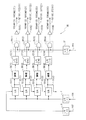
このVスキャン回路36は、レベル変換回路6、7により、第1の電圧系Iの振幅による垂直スタートパルスVST、垂直クロックVCKを第2の電圧系IIの振幅に変換し、シフトレジスタ(S/R)10(1)〜10(4)により、この垂直スタートパルスVSTを垂直クロックVCKで順次転送し、これにより第2の電圧系IIによる選択信号S1(1)〜S1(4)を生成する。
The
Vスキャン回路36は、それぞれ第2の電圧系IIで動作する第1の論理回路38(1)〜38(4)を介して、選択信号S1(1)〜S1(4)をレベル変換回路12(1)〜12(4)に入力して第3の電圧系III の振幅に変換する。なおここでこのレベル変換回路12(1)〜12(4)には、消費電力が少ない図21について上述したレベル変換回路が適用される。
The
Vスキャン回路36は、レベル変換回路37を介して、第1の電圧系Iの振幅による垂直イネーブル信号VENを、第3の電圧系III の振幅に補正する。Vスキャン回路36は、第3の電圧系III で動作する第2の論理回路39(1)〜39(4)に、この第3の電圧系III による垂直イネーブル信号VENを入力し、またレベル変換回路12(1)〜12(4)の出力信号をそれぞれ入力する。Vスキャン回路36は、それぞれ第1の論理回路38(1)〜38(4)、対応する第2の論理回路39(1)〜39(4)による論理演算により、駆動信号S21(1)〜S21(4)、S22(1)〜S22(4)を生成し、論理回路39(1)〜39(4)から出力される駆動信号をインバータ13(1)〜13(4)を介して出力する。
The
なお例えば駆動信号S22のように、単に選択信号S2とイネーブル信号VENとの簡単な論理積によって求めることが可能な駆動信号については、必要に応じて第1の論理回路38(1)〜38(4)を省略してもよい。 For example, a drive signal that can be obtained by a simple logical product of the selection signal S2 and the enable signal VEN, such as the drive signal S22, can be set to the first logic circuits 38 (1) to 38 ( 4) may be omitted.
これに対して水平駆動回路は、図15について上述した水平駆動回路と同一に構成される。 On the other hand, the horizontal drive circuit has the same configuration as the horizontal drive circuit described above with reference to FIG.
(2)実施例の動作
以上の構成において、この実施例のディスプレイ装置では(図15参照)、マトリックス状に画素33を配置して形成された表示部の周囲に設けられ水平駆動回路により、表示部の信号線SIGに各画素33の階調を示す駆動信号Vsigが出力される。またこの駆動信号Vsigの出力に応動して、表示部の周囲に設けられた垂直駆動回路により駆動信号S21〜S24が生成され、この駆動信号S21〜S24により各画素に信号線SIGの信号レベルが設定されると共に、各画素33の動作が制御され、これにより信号線SIGの信号レベルにより各画素33に設けられた有機EL素子34が発光する。これによりこのディスプレイ装置では、所望の画像を表示部2で表示することが可能となる。
(2) Operation of Embodiment In the above configuration, in the display device of this embodiment (see FIG. 15), display is performed by a horizontal drive circuit provided around a display portion formed by arranging pixels 33 in a matrix. The drive signal Vsig indicating the gradation of each pixel 33 is output to the signal line SIG of the part. In response to the output of the drive signal Vsig, drive signals S21 to S24 are generated by a vertical drive circuit provided around the display unit, and the signal level of the signal line SIG is set to each pixel by the drive signals S21 to S24. At the same time, the operation of each pixel 33 is controlled, whereby the
また各画素33では(図2及び図3)、垂直駆動回路による駆動信号S21〜S24によりトランジスタTR1、TR2、TR4、TR5がオンオフ動作し、トランジスタTR4、TR5がオン状態に設定されて信号レベル保持用コンデンサCsの両端電位がそれぞれ所定の固定電位Vofs、Viniに設定された後、垂直駆動回路による駆動信号S23により、信号レベル保持用コンデンサCsのソース側端が固定電位Viniより切り離されると共に、トランジスタTR3が電源VDD1に接続され、これにより信号レベル保持用コンデンサCsの両端電位差がトランジスタTR3のしきい値電圧Vthに設定されて、トランジスタTR3のしきい値電圧Vthのばらつきによる発光輝度のばらつきが防止される。 In each pixel 33 (FIGS. 2 and 3), the transistors TR1, TR2, TR4, and TR5 are turned on and off by the drive signals S21 to S24 from the vertical drive circuit, and the transistors TR4 and TR5 are set to the on state to maintain the signal level. After both end potentials of the capacitor Cs are set to predetermined fixed potentials Vofs and Vini, respectively, the source side end of the signal level holding capacitor Cs is separated from the fixed potential Vini by the drive signal S23 from the vertical drive circuit, and the transistor TR3 is connected to the power supply VDD1, thereby the potential difference between both ends of the signal level holding capacitor Cs is set to the threshold voltage Vth of the transistor TR3, thereby preventing variations in light emission luminance due to variations in the threshold voltage Vth of the transistor TR3. Is done.
その後、画素33は、信号レベル保持用コンデンサCsのゲート側端が信号線SIGに接続され、信号レベル保持用コンデンサCsに信号線SIGの電位Vsigがセットされ、このセットされた電圧に応じた駆動電流で有機EL素子34が発光する。
Thereafter, in the pixel 33, the gate side end of the signal level holding capacitor Cs is connected to the signal line SIG, and the potential Vsig of the signal line SIG is set to the signal level holding capacitor Cs, and driving according to the set voltage is performed. The
画素33は、この信号レベル保持用コンデンサCsに信号線SIGの電位Vsigをセットする際に、信号レベル保持用コンデンサCsのゲート側端を信号線SIGに接続した状態で、一定期間Tの間、トランジスタTR3が電源VDD1に接続され、これによりトランジスタTR3の移動度に応じて信号レベル保持用コンデンサCsの両端電位差を補正した後、この信号レベル保持用コンデンサCsの一端が信号線SIGの信号レベルVsigに設定される。これにより画素33は、トランジスタTR3の移動度のばらつきによる発光輝度のばらつきが防止される。 When setting the potential Vsig of the signal line SIG to the signal level holding capacitor Cs, the pixel 33 is connected to the signal line SIG at the gate side end of the signal level holding capacitor Cs for a certain period T. After the transistor TR3 is connected to the power supply VDD1, thereby correcting the potential difference between both ends of the signal level holding capacitor Cs according to the mobility of the transistor TR3, one end of the signal level holding capacitor Cs is connected to the signal level Vsig of the signal line SIG. Set to As a result, the pixel 33 can be prevented from having variations in emission luminance due to variations in mobility of the transistor TR3.
しかしながらこのように一定期間Tの間、信号レベル保持用コンデンサCsのゲート側端を信号線SIGに接続した状態で、トランジスタTR3を電源VDD1に接続してトランジスタTR3の移動度ばらつきを補正する場合に、この期間Tが各走査線VSCAN1(1)〜VSCAN1(4)でばらついたのでは、画質が劣化することになる。これに対して垂直駆動回路において各走査線VSCAN1(1)〜VSCAN1(4)の駆動信号を生成する従来構成によるVスキャン回路では、走査線VSCAN1(1)〜VSCAN1(4)毎に、第2の電圧系IIによる振幅を第3の電圧系III による振幅に補正するレベル変換回路12(1)〜12(4)が設けられ(図17、図23、図26)、これらレベル変換回路12(1)〜12(4)では、回路間で出力信号におけるタイミングのばらつきが大きい欠点がある。 However, when the transistor TR3 is connected to the power supply VDD1 and the mobility variation of the transistor TR3 is corrected with the gate side end of the signal level holding capacitor Cs connected to the signal line SIG for a certain period T as described above. If the period T varies between the scanning lines VSCAN1 (1) to VSCAN1 (4), the image quality deteriorates. On the other hand, in the V scan circuit according to the conventional configuration that generates the drive signals for the scan lines VSCAN1 (1) to VSCAN1 (4) in the vertical drive circuit, the second scan line VSCAN1 (1) to VSCAN1 (4) Level conversion circuits 12 (1) to 12 (4) for correcting the amplitude of the voltage system II to the amplitude of the third voltage system III are provided (FIGS. 17, 23, and 26). In 1) to 12 (4), there is a disadvantage that the timing variation in the output signal is large between circuits.
従って画素33の駆動信号S21〜S24のうちの、移動度の補正に係る期間Tを決定する駆動信号S21、S22を従来構成によるVスキャン回路で構成したのでは、この期間Tがライン間でばらつくことになり、その結果、ライン間で発光輝度がばらつくようになる。 Therefore, if the drive signals S21 and S22 for determining the period T relating to the mobility correction among the drive signals S21 to S24 of the pixel 33 are configured by the V scan circuit of the conventional configuration, the period T varies between lines. As a result, the light emission luminance varies between the lines.
そこでこの実施例では、少なくとも移動度の補正に係る期間Tを決定する駆動信号S21、S22のVスキャン回路は(図1)、垂直スタートパルスVST、垂直クロックVCKをポリシリコンTFTの駆動に適し、かつ有機EL素子の駆動に適した第3の電圧系III より振幅の小さな第2の電圧系IIで処理し、その処理結果の出力信号と駆動信号S21〜S24において信号レベルの切り換わるタイミングを設定する垂直イネーブル信号VENとを第3の電圧系III の振幅に補正した後、駆動信号S21、S22を生成する。 Therefore, in this embodiment, the V scan circuit of the drive signals S21 and S22 for determining at least the period T related to the mobility correction (FIG. 1) is suitable for driving the polysilicon TFT with the vertical start pulse VST and the vertical clock VCK. In addition, the processing is performed by the second voltage system II having a smaller amplitude than the third voltage system III suitable for driving the organic EL element, and the output signal of the processing result and the timing at which the signal level is switched in the drive signals S21 to S24 are set. After the vertical enable signal VEN to be corrected to the amplitude of the third voltage system III, drive signals S21 and S22 are generated.
この場合、各走査線の系統には、1つのレベル変換回路37により振幅が補正された垂直イネーブル信号VENが供給されることにより、走査線間における駆動信号S21、S22のタイミングのばらつきを有効に回避することができる。従ってディスプレイ装置では、移動度を補正する期間Tのライン間のばらつきを有効に回避して、高い歩留まりで、高画質の画像を表示することができる。
In this case, the vertical enable signal VEN whose amplitude is corrected by one
特に、この移動度のばらつきの補正に係る駆動信号S21、S22のタイミングのばらつきを防止できることにより、走査線間における移動度補正のばらつきを有効に回避することができ、一段と高画質のディスプレイ装置を得ることができる。 In particular, the variation in timing of the drive signals S21 and S22 relating to the correction of the mobility variation can be prevented, so that the mobility correction variation between the scanning lines can be effectively avoided, and a display device with higher image quality can be obtained. Obtainable.
またさらにこの実施例では、選択信号S1(1)〜S1(4)を、有機EL素子の駆動に適した第3の電圧系の振幅に比して小さな、第2の電圧系で処理していることにより、全体を第3の電圧系の振幅で処理する場合に比して、格段的に消費電力、周辺回路の面積の増大を有効に回避することができる。 In this embodiment, the selection signals S1 (1) to S1 (4) are processed by the second voltage system which is smaller than the amplitude of the third voltage system suitable for driving the organic EL element. As a result, the power consumption and the increase in the area of the peripheral circuit can be effectively avoided as compared with the case where the whole is processed with the amplitude of the third voltage system.
(3)実施例の効果
以上の構成によれば、画素の駆動に適した第3の電圧系の振幅より小さな第2の電圧系の振幅で選択信号を生成した後、第3の電圧系の振幅に変換し、この第3の電圧系の振幅による選択信号を基準にして第3の電圧系の振幅による垂直イネーブル信号を処理して駆動信号を生成することにより、消費電力、周辺回路の面積の増大を有効に回避して、従来に比して走査線に出力する駆動信号の精度を向上させることができる。
(3) Effects of the embodiment According to the above configuration, after the selection signal is generated with the amplitude of the second voltage system smaller than the amplitude of the third voltage system suitable for driving the pixel, the third voltage system By converting the signal into amplitude and processing the vertical enable signal based on the amplitude of the third voltage system on the basis of the selection signal based on the amplitude of the third voltage system to generate the drive signal, the power consumption, the area of the peripheral circuit Therefore, the accuracy of the drive signal output to the scanning line can be improved as compared with the conventional case.
また第2の電圧系の振幅より小さな第1の電圧系の振幅による基準パルスである垂直スタートパルスの振幅を第2の電圧系の振幅に変換した後、順次転送して第2の電圧系の振幅による選択信号を生成することにより、この垂直スタートパルスを生成する前段の回路ブロックを汎用の集積回路技術により作成することができる。 In addition, after converting the amplitude of the vertical start pulse, which is a reference pulse based on the amplitude of the first voltage system smaller than the amplitude of the second voltage system, into the amplitude of the second voltage system, it is sequentially transferred to the second voltage system. By generating the selection signal based on the amplitude, the previous circuit block for generating the vertical start pulse can be created by a general-purpose integrated circuit technique.
また少なくともトランジスタの移動度のばらつきによる発光輝度のばらつきを補正する一定期間の駆動信号の生成に適用して、この駆動信号の精度を向上させることにより、移動度のばらつき補正を精度良く実行することができ、高い画質により所望の画像を表示することができる。 In addition, it can be applied to the generation of a drive signal for a fixed period that corrects at least the variation in light emission luminance due to the variation in the mobility of the transistor, and the accuracy of the drive signal is improved so that the mobility variation can be corrected with high accuracy. The desired image can be displayed with high image quality.
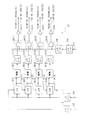
図4は、図1及び図23との対比により、本発明の実施例2のディスプレイ装置に適用されるVスキャン回路を示すブロック図である。この実施例のディスプレイ装置は、図1について上述したVスキャン回路36に代えて、この図4に示すVスキャン回路46が適用される点を除いて、実施例1のディスプレイ装置と同一に構成される。
FIG. 4 is a block diagram showing a V scan circuit applied to the display device according to the second embodiment of the present invention in comparison with FIGS. The display device of this embodiment is configured in the same way as the display device of the first embodiment except that the
このVスキャン回路46は、シフトレジスタ10(1)〜10(4)に代えて、図24について上述したSRラッチ回路構成のシフトレジスタ19(1)〜19(4)により垂直スタートパルスVSTを順次転送する。
In this
この実施例のように、SRラッチ回路構成のシフトレジスタにより垂直スタートパルスVSTを転送して選択信号を生成する場合についても、実施例1と同様の効果を得ることができる。 As in this embodiment, the same effect as that of the first embodiment can be obtained when the vertical start pulse VST is transferred by the shift register having the SR latch circuit configuration to generate the selection signal.
図5は、図1及び図26との対比により、本発明の実施例3のディスプレイ装置に適用されるVスキャン回路を示すブロック図である。この実施例のディスプレイ装置は、図1について上述したVスキャン回路36に代えて、この図4に示すVスキャン回路47が適用される点を除いて、実施例1のディスプレイ装置と同一に構成される。
FIG. 5 is a block diagram showing a V scan circuit applied to the display device according to the third embodiment of the present invention, in comparison with FIGS. 1 and 26. The display device of this embodiment is configured in the same way as the display device of the first embodiment except that the
このVスキャン回路46は、シフトレジスタ10(1)〜10(4)に代えて、デコーダ26により選択信号S1(1)〜S1(4)を生成する。
The
この実施例のように、デコーダにより選択信号を生成する場合についても、実施例1と同様の効果を得ることができる。 As in this embodiment, when the selection signal is generated by the decoder, the same effect as in the first embodiment can be obtained.
図6は、図3との対比により、本発明の実施例4のディスプレイ装置に適用される駆動信号の説明に供するタイムチャートである。この実施例では、移動度を補正する期間Tの終端を決定する駆動信号S21において、信号レベルが徐々に立ち下がるように設定され、これにより信号線SIGに設定された信号レベルVsigが高い場合程、速い時点で、トランジスタTR1がオフ動作するように設定される。この実施例のディスプレイ装置は、この駆動信号S21に関する構成が異なる点を除いて、上述の実施例のディスプレイ装置と同一に構成される。 FIG. 6 is a time chart for explaining drive signals applied to the display device according to the fourth embodiment of the present invention in comparison with FIG. In this embodiment, in the drive signal S21 for determining the end of the period T for correcting the mobility, the signal level is set to gradually fall, and as a result, the signal level Vsig set to the signal line SIG is higher. The transistor TR1 is set to be turned off at a fast time. The display device of this embodiment is configured in the same manner as the display device of the above-described embodiment except that the configuration relating to the drive signal S21 is different.
すなわち実施例1について上述した移動度を補正する期間Tにおいて、トランジスタTR3に流れる電流Idsは、トランジスタTR3のゲートソース間電圧に応じて変化することにより、信号線SIGの信号レベルVsigが高い場合程、すなわち有機EL素子34を高い輝度レベルで発光させる場合程、大きな電流が流れることになる。従って有機EL素子34を高い輝度レベルで発光させる場合程、短い時間で移動度のばらつきを補正できることになる。
That is, in the period T for correcting the mobility described in the first embodiment, the current Ids flowing through the transistor TR3 changes according to the voltage between the gate and the source of the transistor TR3, so that the signal level Sig of the signal line SIG is higher. That is, as the
これによりこの実施例では、移動度を補正する期間Tの終端を決定する駆動信号S21において、信号レベルが徐々に立ち下がるように設定し、有機EL素子34を高い輝度レベルで発光させる場合程、速くトランジスタTR1をオフ動作させ、移動度のばらつきを補正する期間を短くする。このように有機EL素子34を高い輝度レベルで発光させる場合程、移動度のばらつきを補正する期間を短くすれば、一段と画質を向上し、ユニフォーミティーを向上させることができる。なおこの図6では、時間の経過によりほぼ直線的に信号レベルが低下するように駆動信号S21を生成する場合を示しているが、実際上、指数関数的に信号レベルを立ち下げて、適切に移動度のばらつきを補正することができる。
Accordingly, in this embodiment, the drive signal S21 for determining the end of the period T for correcting the mobility is set so that the signal level gradually falls, and the
この実施例では、この駆動信号S21に対応するように、立ち下がり側の信号レベルが徐々に立ち下がるように、所定の信号発生回路で第1の電圧系Iの振幅による垂直イネーブル信号VENが生成される。またアナログ信号処理回路構成の増幅回路により、この電圧系Iの振幅によるイネーブル信号VENを増幅し、第3の電圧系の振幅によるイネーブル信号VENを生成する。この実施例では、この増幅回路がレベル変換回路として機能する。 In this embodiment, the vertical enable signal VEN is generated with the amplitude of the first voltage system I by a predetermined signal generation circuit so that the signal level on the falling side gradually falls so as to correspond to the drive signal S21. Is done. Also, the enable signal VEN having the amplitude of the voltage system I is amplified by the amplifier circuit having the analog signal processing circuit configuration, and the enable signal VEN having the amplitude of the third voltage system is generated. In this embodiment, this amplifier circuit functions as a level conversion circuit.
この実施例では、図1、図4、又は図5のVスキャン回路において、レベル変換回路37が省略され、直接、第3の電圧系の振幅による垂直イネーブル信号VENを論理回路39(1)〜39(4)に入力する。またこの論理回路39(1)〜39(4)をアナログ信号処理回路により構成して、選択信号S1(1)〜S1(4)によりそれぞれ第3の電圧系の振幅によるイネーブル信号VENを選択して駆動信号S21(1)〜S21(4)を生成する。
In this embodiment, in the V scan circuit of FIG. 1, FIG. 4, or FIG. 5, the
なお移動度のばらつきを補正する期間Tの開始時点を定義する駆動信号S22については、上述の実施例と同様に生成する。 The drive signal S22 that defines the start point of the period T for correcting the mobility variation is generated in the same manner as in the above-described embodiment.
この実施例によれば、駆動信号の信号レベルを徐々に立ち下げて、有機EL素子を高い輝度レベルで発光させる場合程、移動度のばらつきを補正する期間を短くして画質を向上する場合にあっても、上述の実施例と同様の効果を得ることができる。 According to this embodiment, when the signal level of the drive signal is gradually lowered and the organic EL element emits light at a higher luminance level, the period for correcting the variation in mobility is shortened to improve the image quality. Even if it exists, the effect similar to the above-mentioned Example can be acquired.
図7は、図2との対比により、本発明の実施例5のディスプレイ装置に適用される画素の構成を示す接続図であり、図8は、この画素53の動作の説明に供するタイムチャートである。
FIG. 7 is a connection diagram illustrating a configuration of a pixel applied to the display device according to the fifth exemplary embodiment of the present invention in comparison with FIG. 2, and FIG. 8 is a time chart for explaining the operation of the
この実施例の画素53は、有機EL素子34を電源VDD1に接続するトランジスタTR2(図2参照)が省略され、電源VDD1の電位を直接制御して、有機EL素子34の発光、非発光が制御される(図8(B)、(D)〜(F))。また信号レベル保持用コンデンサCsを固定電位Viniに接続するトランジスタTR4が省略され、有機EL素子34を介した放電により信号レベル保持用コンデンサCsの有機EL素子34側端の電圧を十分に低い電圧に立ち上げ、トランジスタTR3のしきい値電圧Vthを信号レベル保持用コンデンサCsにセットする(図8(C)、(D)〜(F))。またしきい値電圧Vthを信号レベル保持用コンデンサCsにセットした後も、トランジスタTR3のドレイン電圧を立ち上げたままに保持し、トランジスタTR1のオンオフ制御のみによりトランジスタTR1の移動度のばらつきを補正し、さらには信号線SIGの信号レベルVsigを信号レベル保持用コンデンサCsにセットする(図8(A)、(D)〜(F))。
In the
この画素53の構成に対応して、この実施例の垂直駆動回路は、少なくともトランジスタTR1を駆動する駆動信号S21(1)〜S21(4)が、図1、図4、又は図5のVスキャン回路で生成される。
Corresponding to the configuration of the
この実施例によれば、一段と簡易な構成により画素を構成して、上述の実施例と同様の効果を得ることができる。 According to this embodiment, the pixel can be configured with a simpler configuration, and the same effect as in the above-described embodiment can be obtained.
図9は、図2との対比により、本発明の実施例6のディスプレイ装置に適用される画素の構成を示す接続図であり、図10は、この画素54の動作の説明に供するタイムチャートである。この画素54は、Pチャンネル型トランジスタTR3のソースが正側電源VDD1に接続され、駆動信号S22によりオンオフ動作するトランジスタTR2を介して、このトランジスタTR3のソースが有機EL素子34に接続される。これによりこの画素54は、駆動信号S22によるトランジスタTR2のオンオフ制御により、有機EL素子34の発光、非発光を制御し(図10(B)、(E)〜(G))、さらにはトランジスタTR3のゲートソース間電圧に応じた駆動電流により有機EL素子34を駆動する。
FIG. 9 is a connection diagram illustrating a configuration of a pixel applied to the display device according to the sixth embodiment of the present invention in comparison with FIG. 2, and FIG. 10 is a time chart for explaining the operation of the
またこの有機EL素子34を駆動するトランジスタTR3は、所定のコンデンサCc、信号レベル保持用コンデンサCsの直列回路がゲート及び正側電源VDD1間に設けられ、駆動信号S24によりオンオフ動作するトランジスタTR5を介して、この直列回路の接続中点が固定電位Vofsに接続され、また駆動信号S23によりオンオフ動作するトランジスタTR4によりゲートドレインが短絡される。また駆動信号S21によりオンオフ動作して信号レベル保持用コンデンサCsのコンデンサCc側端を信号線SIGに接続するトランジスタTR1が設けられる。
The transistor TR3 for driving the
画素54は、駆動信号S22によりトランジスタTR2をオフ状態に切り換えて有機EL素子34の発光を停止すると、図10(G)において準備により示すように、一定の期間経過後、駆動信号S24によりトランジスタTR5がオン状態に切り換えられ、信号レベル保持用コンデンサCsのコンデンサCc側端が固定電位Vofsに設定される(図10(D)及び(E))。また駆動信号S22によりトランジスタTR2がオン状態に切り換えられると共に、駆動信号S23によりトランジスタTR4がオン状態に切り換えられ、有機EL素子34を介してコンデンサCsの蓄積電荷を放電し、トランジスタTR3のゲート電圧が立ち下げられる(図10(B)、(C)及び(F))。
When the
画素54は、続いて駆動信号S22によりトランジスタTR2がオフ状態に切り換えられ、これによりトランジスタTR3を介して正側電源VDD1によりコンデンサCcのトランジスタTR3側端が充電され、トランジスタTR3のゲート電圧Vgが徐々に上昇する(図10(B)及び(F))。ここでこのゲート電圧Vgの上昇により、トランジスタTR3のゲート電圧Vgが、正側電源VDD1の電位よりトランジスタTR3のしきい値電圧Vthだけ立ち下がった電圧となると、トランジスタTR3がオフ状態となり、トランジスタTR3を介したコンデンサCcの充電が停止し、これによりゲート電圧Vgの上昇が停止する。これにより画素54は、コンデンサCcにトランジスタTR3のしきい値電圧Vthに対応する電圧をセットし、トランジスタTR3のしきい値電圧Vthのばらつきによる発光輝度のばらつきを防止する。
In the
続いて画素54は、駆動信号S23、S24によりトランジスタTR4、TR5がオフ状態に設定される。その後、画素54は、駆動信号S21によりトランジスタTR1がオン状態に切り換えられ、信号レベル保持用コンデンサCsのコンデンサCc側端の電位が信号線SIGの電位Vsigに設定される。但し、信号線SIGの電位Vsigは、Vofs+Vdataである。これによりトランジスタTR3のゲート電圧Vgは、信号線SIGの電位Vsigに対してコンデンサCcにセットされたしきい値電圧Vthの分だけバイアスされた電圧となり、トランジスタTR3のゲートソース間電圧は、信号線SIGのVsigをしきい値電圧Vthで補正した電圧に設定される。
Subsequently, in the
続いて画素54は、信号レベル保持用コンデンサCsを信号線SIGに接続した状態で、一定期間Tの間、駆動信号S23によりトランジスタTR3がオン状態に切り換えられ、これによりトランジスタTR3を介したコンデンサCcの充電によりトランジスタTR3の移動度が補正される。またその後、駆動信号S23、S21によりトランジスタTR4、TR1が順次オフ状態に切り換えられた後、駆動信号S22によりトランジスタTR2がオン状態に切り換えられて有機EL素子34の駆動が開始される。
Subsequently, in the state where the signal level holding capacitor Cs is connected to the signal line SIG, in the
これによりこの実施例では、移動度のばらつきを補正する駆動信号S23でタイミングがばらつくと、走査線間で移動度のばらつき補正にばらつきが発生し、画質が劣化することになる。そこでこの実施例では、少なくともこの移動度のばらつき補正に係る駆動信号S23が図1、図4、又は図5のVスキャン回路で生成される。 As a result, in this embodiment, if the timing varies with the drive signal S23 for correcting the mobility variation, the mobility variation correction varies between the scanning lines, and the image quality deteriorates. Therefore, in this embodiment, at least the drive signal S23 related to the mobility variation correction is generated by the V scan circuit of FIG. 1, FIG. 4, or FIG.
この実施例によれば、Pチャンネル型トランジスタTR3により有機EL素子34を駆動する場合でも、上述の実施例と同様の効果を得ることができる。
According to this embodiment, even when the
図11は、図1との対比により、本発明の実施例7のディスプレイ装置に適用されるVスキャン回路を示すブロック図である。この実施例のディスプレイ装置は、上述した各実施例のVスキャン回路に代えて、この図11に示すVスキャン回路66が適用される点を除いて、上述の各実施例のディスプレイ装置と同一に構成される。
FIG. 11 is a block diagram showing a V scan circuit applied to the display device according to the seventh embodiment of the present invention in comparison with FIG. The display device of this embodiment is the same as the display device of each embodiment described above except that the
ここでこのVスキャン回路66は、直接、第2の電圧系により垂直スタートパルスVST、垂直クロックVCKが入力される点を除いて、実施例1のVスキャン回路36と同一に構成される。
Here, the
この実施例のように、第2の電圧系により垂直スタートパルスVST、垂直クロックVCKを入力するようにしても、上述の実施例と同様の効果を得ることができる。 Even if the vertical start pulse VST and the vertical clock VCK are input by the second voltage system as in this embodiment, the same effect as in the above-described embodiment can be obtained.
図12は、図1との対比により、本発明の実施例8のディスプレイ装置に適用されるVスキャン回路を示すブロック図である。この実施例のディスプレイ装置は、上述した各実施例のVスキャン回路に代えて、この図12に示すVスキャン回路67が適用される点を除いて、上述の各実施例のディスプレイ装置と同一に構成される。
FIG. 12 is a block diagram showing a V scan circuit applied to the display device according to the eighth embodiment of the present invention in comparison with FIG. The display device of this embodiment is the same as the display device of each embodiment described above except that the
ここでこのVスキャン回路67は、第1の電圧系によるイネーブル信号VENをレベル変換回路37Aにより第2の電圧系の振幅に変換した後、続くレベル変換回路37Bにより第3の電圧系の振幅に変換する。
Here, the
この実施例のようにイネーブル信号を第2の電圧系の振幅に変換した後、第3の電圧系の振幅に変換するようにして、上述の実施例と同様の効果を得ることができる。 As in this embodiment, after the enable signal is converted into the amplitude of the second voltage system, it is converted into the amplitude of the third voltage system, and the same effect as in the above-described embodiment can be obtained.
図13は、図1との対比により、本発明の実施例9のディスプレイ装置に適用されるVスキャン回路を示すブロック図である。この実施例のディスプレイ装置は、上述した各実施例のVスキャン回路に代えて、この図13に示すVスキャン回路68が適用される点を除いて、上述の各実施例のディスプレイ装置と同一に構成される。
FIG. 13 is a block diagram showing a V-scan circuit applied to the display device according to the ninth embodiment of the present invention in comparison with FIG. The display device of this embodiment is the same as the display device of each embodiment described above except that the
ここでこのVスキャン回路69は、論理回路39(1)〜39(4)をグループ化し、各グループ毎にバッファ69(1)、69(2)を介してイネーブル信号VENを論理回路39(1)〜39(4)を入力する。なおこの場合、図13との対比により図14に示すように、バッファ69(1)、69(2)の出力ラインを接続するようにしてもよい。
Here, the
この実施例のように論理回路をグループ化して駆動するようにしても、上述の実施例と同様の効果を得ることができる。 Even if the logic circuits are grouped and driven as in this embodiment, the same effects as in the above-described embodiment can be obtained.
なお上述の実施例においては、トランジスタTR1及びTR2の制御に係る駆動信号等をそれぞれ図1等に示すVスキャン回路で構成する場合について述べたが、本発明はこれに限らず、実用上十分に駆動信号の精度の劣化を許容できる場合には、何れかの駆動信号のVスキャン回路にのみに本発明を適用するようにしてもよい。 In the above-described embodiment, the case where the drive signals and the like related to the control of the transistors TR1 and TR2 are each configured by the V scan circuit shown in FIG. 1 and the like has been described. If the deterioration of the accuracy of the drive signal can be tolerated, the present invention may be applied only to the V scan circuit of any drive signal.
また上述の実施例では、垂直同期信号に同期した垂直スタートパルスを基準パルスに適用してVスキャン回路で処理する場合について述べたが、本発明はこれに限らず、走査線の駆動信号の生成基準である各種基準パルスを処理して駆動信号を生成するVスキャン回路に広く適用することができる。 In the above-described embodiment, the case where the vertical start pulse synchronized with the vertical synchronization signal is applied to the reference pulse and processed by the V scan circuit has been described. However, the present invention is not limited to this, and the generation of the scanning line drive signal is performed. The present invention can be widely applied to a V scan circuit that processes various reference pulses as a reference to generate a drive signal.
なお上述の実施例においては、各種の画素回路により画素を構成する場合について述べたが、本発明はこれに限らず、上述した以外の各種の画素回路により画素を構成する場合にも広く適用することができる。 In the above-described embodiments, the case where the pixel is configured by various pixel circuits has been described. However, the present invention is not limited to this, and the present invention is widely applied to the case where the pixel is configured by various pixel circuits other than those described above. be able to.
また上述の実施例においては、本発明を有機EL素子によるディスプレイ装置に適用する場合について述べたが、本発明はこれに限らず、電流駆動型の種々の発光素子によるディスプレイ装置、さらには液晶等のディスプレイ装置にも広く適用することができる。 In the above-described embodiments, the case where the present invention is applied to a display device using an organic EL element has been described. However, the present invention is not limited thereto, and the display device includes various current-driven light emitting elements, and further includes a liquid crystal display. The present invention can be widely applied to other display devices.
本発明は、例えばポリシリコンTFT(Thin Film Transistor)を用いた有機EL(Electro Luminescence)素子によるアクティブマトリックス型のディスプレイ装置に適用することができる。 The present invention can be applied to an active matrix display device using an organic EL (Electro Luminescence) element using, for example, a polysilicon TFT (Thin Film Transistor).
1……ディスプレイ装置、2……表示部、3、33、53、54……画素、4……Hスキャン回路、5、18、36、46、47、66、67、68、69……Vスキャン回路、6、7、8、12(1)〜12(4)、37、37A、37B……レベル変換回路、10(1)〜10(4)、19(1)〜19(4)……シフトレジスタ、11(1)〜11(4)、38(1)〜38(4)、39(1)〜39(4)……論理回路、26……デコーダ、TR1〜TR10……トランジスタ、Cc、Cs……コンデンサ
DESCRIPTION OF
Claims (8)
前記垂直駆動回路は、
基準パルスを処理して、前記画素の駆動に適した第3の電圧系の振幅より小さな第2の電圧系の振幅により、前記走査線毎に、前記走査線を順次選択する選択信号を生成する選択信号生成回路と、
前記走査線毎に、前記第2の電圧系の振幅による前記選択信号を前記第3の電圧系の振幅に変換する走査線毎のレベル変換回路と、
前記走査線毎に、前記走査線毎のレベル変換回路の出力信号をそれぞれ基準にして、前記駆動信号において信号レベルの切り換わるタイミングを設定する前記第3の電圧系の振幅による垂直イネーブル信号を処理することにより、前記第3の電圧系により前記駆動信号を生成する走査線毎の駆動信号生成回路とを備える
ことを特徴とする表示装置。 In a display device that displays a desired image on the display unit by driving the pixel by outputting a drive signal from a vertical drive circuit to a scanning line of the display unit formed by arranging pixels in a matrix.
The vertical drive circuit includes:
A reference pulse is processed to generate a selection signal for sequentially selecting the scanning lines for each scanning line with the amplitude of the second voltage system smaller than the amplitude of the third voltage system suitable for driving the pixels. A selection signal generation circuit;
A level conversion circuit for each scanning line for converting the selection signal based on the amplitude of the second voltage system into the amplitude of the third voltage system for each scanning line;
For each scanning line, the vertical enable signal based on the amplitude of the third voltage system for setting the timing of switching the signal level in the drive signal is processed with reference to the output signal of the level conversion circuit for each scanning line. Thus, a display device comprising: a drive signal generation circuit for each scanning line that generates the drive signal by the third voltage system.
前記第2の電圧系の振幅より小さな第1の電圧系の振幅による前記基準パルスの振幅を、前記第2の電圧系の振幅に変換する基準パルスのレベル変換回路と、
前記第2の電圧系による基準パルスを順次転送して前記第2の電圧系の振幅による前記選択信号を生成するシフトレジスタとを有する
ことを特徴とする請求項1に記載の表示装置。 The selection signal generation circuit includes:
A reference pulse level conversion circuit that converts the amplitude of the reference pulse with the amplitude of the first voltage system smaller than the amplitude of the second voltage system into the amplitude of the second voltage system;
The display device according to claim 1, further comprising: a shift register that sequentially transfers reference pulses based on the second voltage system to generate the selection signal based on the amplitude of the second voltage system.
前記第2の電圧系の振幅より小さな第1の電圧系の振幅による前記基準パルスの振幅を、前記第2の電圧系の振幅に変換する基準パルスのレベル変換回路と、
前記第2の電圧系による基準パルスと垂直クロックとを処理して、前記第2の電圧系の振幅による前記選択信号を生成するデコーダとを有する
ことを特徴とする請求項1に記載の表示装置。 The selection signal generation circuit includes:
A reference pulse level conversion circuit that converts the amplitude of the reference pulse with the amplitude of the first voltage system smaller than the amplitude of the second voltage system into the amplitude of the second voltage system;
The display device according to claim 1, further comprising: a decoder that processes a reference pulse and a vertical clock generated by the second voltage system to generate the selection signal based on an amplitude of the second voltage system. .
ことを特徴とする請求項1に記載の表示装置。 The display device according to claim 1, wherein the reference pulse is a vertical start pulse synchronized with a vertical synchronization signal.
ことを特徴とする請求項1に記載の表示装置。 A vertical enable signal level converting circuit for converting the amplitude of the vertical enable signal from the amplitude of the first voltage system smaller than the amplitude of the second voltage system to the amplitude of the third voltage system; The display device according to claim 1.
前記垂直イネーブル信号を第1の電圧系の振幅で入力して前記第2の電圧系の振幅に変換した後、前記第2の電圧系の振幅の前記垂直イネーブル信号を前記第3の電圧系の振幅に変換する
ことを特徴とする請求項5に記載の表示装置。 The level conversion circuit for the vertical enable signal includes:
After the vertical enable signal is inputted with the amplitude of the first voltage system and converted into the amplitude of the second voltage system, the vertical enable signal having the amplitude of the second voltage system is converted to the third voltage system. The display device according to claim 5, wherein the display device converts the amplitude.
電流駆動型の発光素子と、
信号レベル保持用のコンデンサと、
前記信号レベル保持用のコンデンサの端子間電圧に応じて前記発光素子を駆動する駆動用トランジスタと、
前記信号レベル保持用のコンデンサの一端を信号線に接続することにより、前記信号線の電位に前記一端の電位を設定する信号線用のトランジスタとを有し、
一定期間、前記駆動用トランジスタにより前記信号線用のコンデンサの端子間電圧を変化させることにより、前記駆動用トランジスタの移動度のばらつきを補正した後、前記信号レベル保持用のコンデンサの端子間電圧に応じた電流で前記発光素子を発光させ、
前記駆動信号が、
前記信号線用のトランジスタ及び又は前記駆動用のトランジスタを駆動する信号である
ことを特徴とする請求項1に記載の表示装置。 The pixel is
A current-driven light emitting device;
A capacitor for holding the signal level;
A driving transistor for driving the light emitting element in accordance with a voltage across terminals of the signal level holding capacitor;
A signal line transistor for setting the potential of the one end to the potential of the signal line by connecting one end of the signal level holding capacitor to the signal line;
After correcting the variation in mobility of the driving transistor by changing the voltage between the terminals of the signal line capacitor by the driving transistor for a certain period, the voltage between the terminals of the signal level holding capacitor is corrected. The light emitting element is caused to emit light with a corresponding current,
The drive signal is
The display device according to claim 1, wherein the display device is a signal for driving the transistor for the signal line and / or the transistor for driving.
基準パルスを処理して、前記画素の駆動に適した第3の電圧系の振幅より小さな第2の電圧系の振幅により、前記走査線毎に、前記走査線を順次選択する選択信号を生成する選択信号生成のステップと、
前記走査線毎に、前記第2の電圧系の振幅による前記選択信号を前記第3の電圧系の振幅に変換する走査線毎のレベル変換のステップと、
前記走査線毎に、前記走査線毎のレベル変換のステップによる出力信号をそれぞれ基準にして、前記駆動信号において信号レベルの切り換わるタイミングを設定する前記第3の電圧系の振幅による垂直イネーブル信号を処理することにより、前記第3の電圧系により前記駆動信号を生成する走査線毎の駆動信号生成のステップとを有する
ことを特徴とする表示装置の駆動方法。
Driving a display device that displays a desired image on the display unit by driving the pixel by outputting a drive signal from a vertical drive circuit to a scanning line of the display unit formed by arranging pixels in a matrix. In the method
A reference pulse is processed to generate a selection signal for sequentially selecting the scanning lines for each scanning line with the amplitude of the second voltage system smaller than the amplitude of the third voltage system suitable for driving the pixels. A step of generating a selection signal;
A level conversion step for each scanning line for converting the selection signal based on the amplitude of the second voltage system into the amplitude of the third voltage system for each scanning line;
For each scanning line, a vertical enable signal based on the amplitude of the third voltage system that sets a timing for switching the signal level in the drive signal with reference to an output signal from the level conversion step for each scanning line. And a step of generating a drive signal for each scanning line for generating the drive signal by the third voltage system by processing. A method for driving a display device, comprising:
Priority Applications (1)
| Application Number | Priority Date | Filing Date | Title |
|---|---|---|---|
| JP2007131210A JP2008286963A (en) | 2007-05-17 | 2007-05-17 | Display device and driving method of display device |
Applications Claiming Priority (1)
| Application Number | Priority Date | Filing Date | Title |
|---|---|---|---|
| JP2007131210A JP2008286963A (en) | 2007-05-17 | 2007-05-17 | Display device and driving method of display device |
Publications (2)
| Publication Number | Publication Date |
|---|---|
| JP2008286963A true JP2008286963A (en) | 2008-11-27 |
| JP2008286963A5 JP2008286963A5 (en) | 2010-06-24 |
Family
ID=40146754
Family Applications (1)
| Application Number | Title | Priority Date | Filing Date |
|---|---|---|---|
| JP2007131210A Pending JP2008286963A (en) | 2007-05-17 | 2007-05-17 | Display device and driving method of display device |
Country Status (1)
| Country | Link |
|---|---|
| JP (1) | JP2008286963A (en) |
Cited By (2)
| Publication number | Priority date | Publication date | Assignee | Title |
|---|---|---|---|---|
| JP2009115840A (en) * | 2007-11-01 | 2009-05-28 | Toshiba Matsushita Display Technology Co Ltd | Active matrix display device and method for driving same |
| CN101908310A (en) * | 2009-06-04 | 2010-12-08 | 索尼公司 | Pixel selection control method, driving circuit, display device and electronic equipment |
Citations (8)
| Publication number | Priority date | Publication date | Assignee | Title |
|---|---|---|---|---|
| JPH09154087A (en) * | 1995-09-28 | 1997-06-10 | Toshiba Electron Eng Corp | Display control device and display control method |
| JP2002514320A (en) * | 1997-04-23 | 2002-05-14 | サーノフ コーポレイション | Active matrix light emitting diode pixel structure and method |
| JP2002351415A (en) * | 2001-05-24 | 2002-12-06 | Seiko Epson Corp | Scan drive circuit, display device, electro-optical device, and scan drive method |
| JP2003186438A (en) * | 2001-12-19 | 2003-07-04 | Hitachi Ltd | Image display device |
| JP2006031032A (en) * | 1999-01-08 | 2006-02-02 | Semiconductor Energy Lab Co Ltd | Semiconductor display device and driving circuit therefor |
| JP2006284798A (en) * | 2005-03-31 | 2006-10-19 | Sanyo Electric Co Ltd | Display device and driving method of display device |
| JP2007034000A (en) * | 2005-07-28 | 2007-02-08 | Sony Corp | Display device |
| JP2007101900A (en) * | 2005-10-04 | 2007-04-19 | Sanyo Electric Co Ltd | Display device |
-
2007
- 2007-05-17 JP JP2007131210A patent/JP2008286963A/en active Pending
Patent Citations (8)
| Publication number | Priority date | Publication date | Assignee | Title |
|---|---|---|---|---|
| JPH09154087A (en) * | 1995-09-28 | 1997-06-10 | Toshiba Electron Eng Corp | Display control device and display control method |
| JP2002514320A (en) * | 1997-04-23 | 2002-05-14 | サーノフ コーポレイション | Active matrix light emitting diode pixel structure and method |
| JP2006031032A (en) * | 1999-01-08 | 2006-02-02 | Semiconductor Energy Lab Co Ltd | Semiconductor display device and driving circuit therefor |
| JP2002351415A (en) * | 2001-05-24 | 2002-12-06 | Seiko Epson Corp | Scan drive circuit, display device, electro-optical device, and scan drive method |
| JP2003186438A (en) * | 2001-12-19 | 2003-07-04 | Hitachi Ltd | Image display device |
| JP2006284798A (en) * | 2005-03-31 | 2006-10-19 | Sanyo Electric Co Ltd | Display device and driving method of display device |
| JP2007034000A (en) * | 2005-07-28 | 2007-02-08 | Sony Corp | Display device |
| JP2007101900A (en) * | 2005-10-04 | 2007-04-19 | Sanyo Electric Co Ltd | Display device |
Cited By (8)
| Publication number | Priority date | Publication date | Assignee | Title |
|---|---|---|---|---|
| JP2009115840A (en) * | 2007-11-01 | 2009-05-28 | Toshiba Matsushita Display Technology Co Ltd | Active matrix display device and method for driving same |
| CN101908310A (en) * | 2009-06-04 | 2010-12-08 | 索尼公司 | Pixel selection control method, driving circuit, display device and electronic equipment |
| CN101908310B (en) * | 2009-06-04 | 2013-05-15 | 索尼公司 | Pixel selection control method, driving circuit, display apparatus, and electronic instrument |
| US8922462B2 (en) | 2009-06-04 | 2014-12-30 | Sony Corporation | Pixel selection control method, driving circuit, display apparatus, and electronic instrument |
| US9171502B2 (en) | 2009-06-04 | 2015-10-27 | Sony Corporation | Pixel selection control method, driving circuit, display apparatus and electronic instrument |
| US9305490B2 (en) | 2009-06-04 | 2016-04-05 | Sony Corporation | Pixel selection control method, driving circuit, display apparatus and electronic instrument |
| US9576534B2 (en) | 2009-06-04 | 2017-02-21 | Sony Corporation | Pixel selection control method, driving circuit, display apparatus and electronic instrument |
| US9990884B2 (en) | 2009-06-04 | 2018-06-05 | Sony Corporation | Pixel selection control method, driving circuit, display apparatus and electronic instrument |
Similar Documents
| Publication | Publication Date | Title |
|---|---|---|
| US11830438B2 (en) | Display device | |
| KR102597752B1 (en) | Organic Light Emitting Display | |
| JP3800050B2 (en) | Display device drive circuit | |
| JP4915195B2 (en) | Display device | |
| JP4826598B2 (en) | Image display device and driving method of image display device | |
| JP5726325B2 (en) | Display device and driving method thereof | |
| US20200090590A1 (en) | Display device and method of driving display device | |
| JP2011135523A (en) | Drive circuit and display device | |
| KR20090028429A (en) | Display device and driving method | |
| KR20190048735A (en) | Display panel | |
| US8659522B2 (en) | Display apparatus having a threshold voltage and mobility correcting period and method of driving the same | |
| JP2011150270A (en) | Drive circuit and display device | |
| US8610647B2 (en) | Image display apparatus and method of driving the image display apparatus | |
| JP2010276783A (en) | Active matrix type display | |
| JP5678730B2 (en) | Inverter circuit and display device | |
| JP5532301B2 (en) | Driving circuit and display device | |
| JP2008286963A (en) | Display device and driving method of display device | |
| JP2008197279A (en) | Active matrix display device | |
| US12236862B2 (en) | Display device and method for driving same | |
| JP4915194B2 (en) | Display device | |
| JP5637046B2 (en) | Inverter circuit and display device | |
| JP5589904B2 (en) | Inverter circuit and display device | |
| JP2008122498A (en) | Display panel drive circuit, display device, and pixel circuit drive method | |
| JP5589903B2 (en) | Inverter circuit and display device | |
| JP5454919B2 (en) | Logic circuit and display device |
Legal Events
| Date | Code | Title | Description |
|---|---|---|---|
| A521 | Request for written amendment filed |
Free format text: JAPANESE INTERMEDIATE CODE: A523 Effective date: 20090127 |
|
| RD03 | Notification of appointment of power of attorney |
Free format text: JAPANESE INTERMEDIATE CODE: A7423 Effective date: 20090331 |
|
| RD04 | Notification of resignation of power of attorney |
Free format text: JAPANESE INTERMEDIATE CODE: A7424 Effective date: 20090403 |
|
| A521 | Request for written amendment filed |
Free format text: JAPANESE INTERMEDIATE CODE: A523 Effective date: 20100510 |
|
| A621 | Written request for application examination |
Free format text: JAPANESE INTERMEDIATE CODE: A621 Effective date: 20100510 |
|
| A977 | Report on retrieval |
Free format text: JAPANESE INTERMEDIATE CODE: A971007 Effective date: 20120316 |
|
| A131 | Notification of reasons for refusal |
Free format text: JAPANESE INTERMEDIATE CODE: A131 Effective date: 20120321 |
|
| A521 | Request for written amendment filed |
Free format text: JAPANESE INTERMEDIATE CODE: A523 Effective date: 20120515 |
|
| A131 | Notification of reasons for refusal |
Free format text: JAPANESE INTERMEDIATE CODE: A131 Effective date: 20120605 |
|
| A02 | Decision of refusal |
Free format text: JAPANESE INTERMEDIATE CODE: A02 Effective date: 20121225 |