JP2008243934A - Semiconductor substrate, method for manufacturing the same, and ultraviolet light emitting device - Google Patents
Semiconductor substrate, method for manufacturing the same, and ultraviolet light emitting device Download PDFInfo
- Publication number
- JP2008243934A JP2008243934A JP2007079117A JP2007079117A JP2008243934A JP 2008243934 A JP2008243934 A JP 2008243934A JP 2007079117 A JP2007079117 A JP 2007079117A JP 2007079117 A JP2007079117 A JP 2007079117A JP 2008243934 A JP2008243934 A JP 2008243934A
- Authority
- JP
- Japan
- Prior art keywords
- semiconductor layer
- base material
- semiconductor substrate
- semiconductor
- substrate
- Prior art date
- Legal status (The legal status is an assumption and is not a legal conclusion. Google has not performed a legal analysis and makes no representation as to the accuracy of the status listed.)
- Pending
Links
- 239000004065 semiconductor Substances 0.000 title claims abstract description 218
- 239000000758 substrate Substances 0.000 title claims abstract description 91
- 238000000034 method Methods 0.000 title claims abstract description 59
- 238000004519 manufacturing process Methods 0.000 title claims abstract description 28
- 239000000463 material Substances 0.000 claims abstract description 62
- 239000010948 rhodium Substances 0.000 claims abstract description 51
- 150000004767 nitrides Chemical class 0.000 claims abstract description 34
- MHOVAHRLVXNVSD-UHFFFAOYSA-N rhodium atom Chemical compound [Rh] MHOVAHRLVXNVSD-UHFFFAOYSA-N 0.000 claims abstract description 31
- 229910052703 rhodium Inorganic materials 0.000 claims abstract description 30
- 230000015572 biosynthetic process Effects 0.000 claims description 34
- 239000010409 thin film Substances 0.000 claims description 17
- 238000005498 polishing Methods 0.000 claims description 12
- 239000000126 substance Substances 0.000 claims description 11
- 239000013078 crystal Substances 0.000 claims description 10
- 238000004544 sputter deposition Methods 0.000 claims description 5
- 229910052782 aluminium Inorganic materials 0.000 claims description 2
- 229910052733 gallium Inorganic materials 0.000 claims description 2
- 229910052738 indium Inorganic materials 0.000 claims description 2
- 238000006243 chemical reaction Methods 0.000 abstract description 20
- 238000002310 reflectometry Methods 0.000 abstract description 13
- 230000017525 heat dissipation Effects 0.000 abstract description 9
- 229910052751 metal Inorganic materials 0.000 abstract description 9
- 239000002184 metal Substances 0.000 abstract description 9
- PMHQVHHXPFUNSP-UHFFFAOYSA-M copper(1+);methylsulfanylmethane;bromide Chemical compound Br[Cu].CSC PMHQVHHXPFUNSP-UHFFFAOYSA-M 0.000 description 31
- 238000002128 reflection high energy electron diffraction Methods 0.000 description 12
- 229910052594 sapphire Inorganic materials 0.000 description 11
- 239000010980 sapphire Substances 0.000 description 11
- 238000004549 pulsed laser deposition Methods 0.000 description 10
- JMASRVWKEDWRBT-UHFFFAOYSA-N Gallium nitride Chemical compound [Ga]#N JMASRVWKEDWRBT-UHFFFAOYSA-N 0.000 description 8
- 229910002601 GaN Inorganic materials 0.000 description 7
- 238000000026 X-ray photoelectron spectrum Methods 0.000 description 6
- 238000010438 heat treatment Methods 0.000 description 6
- 230000003287 optical effect Effects 0.000 description 6
- 238000004833 X-ray photoelectron spectroscopy Methods 0.000 description 5
- 125000004429 atom Chemical group 0.000 description 5
- 238000000605 extraction Methods 0.000 description 5
- 125000005842 heteroatom Chemical group 0.000 description 5
- 238000010406 interfacial reaction Methods 0.000 description 5
- OKTJSMMVPCPJKN-UHFFFAOYSA-N Carbon Chemical compound [C] OKTJSMMVPCPJKN-UHFFFAOYSA-N 0.000 description 4
- QVGXLLKOCUKJST-UHFFFAOYSA-N atomic oxygen Chemical compound [O] QVGXLLKOCUKJST-UHFFFAOYSA-N 0.000 description 4
- 229910052799 carbon Inorganic materials 0.000 description 4
- 229910052760 oxygen Inorganic materials 0.000 description 4
- 239000001301 oxygen Substances 0.000 description 4
- 238000007741 pulsed electron deposition Methods 0.000 description 4
- BQCADISMDOOEFD-UHFFFAOYSA-N Silver Chemical compound [Ag] BQCADISMDOOEFD-UHFFFAOYSA-N 0.000 description 3
- 238000004458 analytical method Methods 0.000 description 3
- 229910052709 silver Inorganic materials 0.000 description 3
- 239000004332 silver Substances 0.000 description 3
- RYGMFSIKBFXOCR-UHFFFAOYSA-N Copper Chemical compound [Cu] RYGMFSIKBFXOCR-UHFFFAOYSA-N 0.000 description 2
- 238000011109 contamination Methods 0.000 description 2
- 238000007796 conventional method Methods 0.000 description 2
- 229910052802 copper Inorganic materials 0.000 description 2
- 239000010949 copper Substances 0.000 description 2
- 229910003460 diamond Inorganic materials 0.000 description 2
- 239000010432 diamond Substances 0.000 description 2
- 238000009792 diffusion process Methods 0.000 description 2
- 238000001451 molecular beam epitaxy Methods 0.000 description 2
- 238000001579 optical reflectometry Methods 0.000 description 2
- 239000002245 particle Substances 0.000 description 2
- 238000012545 processing Methods 0.000 description 2
- 229910052710 silicon Inorganic materials 0.000 description 2
- 239000010703 silicon Substances 0.000 description 2
- 239000002002 slurry Substances 0.000 description 2
- PIGFYZPCRLYGLF-UHFFFAOYSA-N Aluminum nitride Chemical compound [Al]#N PIGFYZPCRLYGLF-UHFFFAOYSA-N 0.000 description 1
- 238000005229 chemical vapour deposition Methods 0.000 description 1
- 150000001875 compounds Chemical class 0.000 description 1
- 239000004020 conductor Substances 0.000 description 1
- 230000003247 decreasing effect Effects 0.000 description 1
- 238000000151 deposition Methods 0.000 description 1
- 230000000694 effects Effects 0.000 description 1
- 238000009713 electroplating Methods 0.000 description 1
- 239000011521 glass Substances 0.000 description 1
- 239000011810 insulating material Substances 0.000 description 1
- 238000005259 measurement Methods 0.000 description 1
- 239000000203 mixture Substances 0.000 description 1
- 238000012986 modification Methods 0.000 description 1
- 230000004048 modification Effects 0.000 description 1
- 239000012299 nitrogen atmosphere Substances 0.000 description 1
- 239000003960 organic solvent Substances 0.000 description 1
- 238000009304 pastoral farming Methods 0.000 description 1
Images


Landscapes
- Led Devices (AREA)
Abstract
【課題】熱放散が良好でかつ紫外光等の短波長領域の光に対する基材の反射性を向上することができ、III族窒化物の半導体層と金属の基材との間に界面反応層が形成されない高品質な半導体基板とその製造方法を提供する。
【解決手段】ロジウムからなる基材2と、基材2の表面にIII族窒化物からなる半導体層3とを備えたことを特徴とする。
【選択図】図1An interface reaction layer between a group III nitride semiconductor layer and a metal substrate, which has good heat dissipation and can improve the reflectivity of the substrate with respect to light in a short wavelength region such as ultraviolet light. Provided is a high-quality semiconductor substrate in which no is formed and a method for manufacturing the same.
A base material 2 made of rhodium and a semiconductor layer 3 made of a group III nitride on the surface of the base material 2 are provided.
[Selection] Figure 1
Description
この発明は、半導体基板とその製造方法および紫外線発光装置に関するものである。 The present invention relates to a semiconductor substrate, a manufacturing method thereof, and an ultraviolet light emitting device.
近年、短波長の光学素子として、ガリウム窒化物(GaN)、アルミニウム窒化物(AlN)、およびこれらの化合物が注目されている。従来から、これらのIII族窒化物の半導体層を成長させるための基材としてサファイアが広く用いられている。サファイアは化学的な安定性が高いという利点があるが、一方で熱伝導率が低いという課題があり、基材上に形成した光学素子等の半導体素子の性能を低下させる要因となっている。
このため、III族窒化物の半導体層を成長させる基材として、熱伝導率の高い金属等を用いて熱放散を改善し、基材上の半導体素子の性能を改善できる半導体基板が知られている。このような半導体基板としては、サファイア基板上に形成した半導体層をレーザリフトオフ法により剥離させ、銅やシリコン等の高熱伝導率の基材上に移設するものが知られている。(例えば、非特許文献1参照)。
In recent years, gallium nitride (GaN), aluminum nitride (AlN), and compounds thereof have attracted attention as short-wavelength optical elements. Conventionally, sapphire has been widely used as a base material for growing these group III nitride semiconductor layers. Sapphire has the advantage of high chemical stability, but on the other hand, there is a problem that the thermal conductivity is low, which is a factor that degrades the performance of semiconductor elements such as optical elements formed on a substrate.
For this reason, as a base material for growing a group III nitride semiconductor layer, a semiconductor substrate is known which can improve heat dissipation by using a metal having high thermal conductivity and improve the performance of a semiconductor element on the base material. Yes. As such a semiconductor substrate, one in which a semiconductor layer formed on a sapphire substrate is peeled off by a laser lift-off method and transferred onto a high thermal conductivity base material such as copper or silicon is known. (For example, refer nonpatent literature 1).
また、近年、基材上に形成した光学素子の光取り出し効率を向上させることが望まれている。上述の非特許文献1では、光反射性の高い銀(Ag)の基材上に光学素子を形成することで、光学素子から基材側に発せられる光を反射させ、光取り出し効率の向上を図っている。
しかし、上述の非特許文献1では、サファイア基板上に形成した半導体層を剥離させ、別の基材上に移設する工程を必要とするため、製造工程が複雑で製造が困難であるだけでなく、歩留まりが著しく低下する。このため、金属の基材上に、III族窒化物の半導体層を直接成長させる技術が要望されている。
However, in the above-mentioned Non-Patent
しかしながら、例えば、MOCVD法等の従来の技術を用いて金属の基材上にIII族窒化物の半導体層を形成した場合、III族窒化物と金属の基材との間で深刻な界面反応が生じ、半導体素子の性能が著しく低下するという課題がある。
また、光学素子の光取り出し効率を向上させるために基材としてAgを用いた場合、可視光領域における光反射性は良好であるが、紫外光等の短波長領域における光反射性が著しく低下するという課題がある。
However, for example, when a group III nitride semiconductor layer is formed on a metal substrate using a conventional technique such as MOCVD, a serious interface reaction occurs between the group III nitride and the metal substrate. As a result, there is a problem in that the performance of the semiconductor element is significantly reduced.
In addition, when Ag is used as the base material in order to improve the light extraction efficiency of the optical element, the light reflectivity in the visible light region is good, but the light reflectivity in the short wavelength region such as ultraviolet light is significantly reduced. There is a problem.
そこで、この発明は、熱放散が良好でかつ紫外光等の短波長領域の光に対する基材の反射性を向上することができ、III族窒化物の半導体層と金属の基材との間に界面反応層が形成されない高品質な半導体基板とその製造方法を提供するものである。 Therefore, the present invention has good heat dissipation and can improve the reflectivity of the substrate with respect to light in a short wavelength region such as ultraviolet light, and between the group III nitride semiconductor layer and the metal substrate. The present invention provides a high-quality semiconductor substrate on which no interface reaction layer is formed and a method for manufacturing the same.
上記の課題を解決するために、本発明の半導体基板は、ロジウムからなる基材と、前記基材の表面にIII族窒化物からなる半導体層とを備えたことを特徴とする。
このように構成することで、サファイア等と比較して熱伝導性に優れ、銀(Ag)等と比較して紫外線等の短波長の光に対する反射性に優れたロジウム(Rh)上にIII族窒化物の半導体層が形成される。
したがって、半導体基板の熱放散をサファイア等の基材を用いた場合よりも大幅に向上させることができるだけでなく、紫外線等の短波長の光に対する基材の反射性をAg等の基材を用いた場合よりも大幅に向上させることができる。また、基材上に形成された半導体層を用いて基材上に半導体素子を形成することができる。
In order to solve the above problems, a semiconductor substrate of the present invention is characterized by comprising a base material made of rhodium and a semiconductor layer made of a group III nitride on the surface of the base material.
By comprising in this way, it is excellent in heat conductivity compared with sapphire etc., and is group III on rhodium (Rh) excellent in reflectivity with respect to light of short wavelengths, such as ultraviolet rays, compared with silver (Ag) etc. A nitride semiconductor layer is formed.
Therefore, the heat dissipation of the semiconductor substrate can be greatly improved as compared with the case where a base material such as sapphire is used, and the base material such as Ag is used for the reflectivity of the base material with respect to short wavelength light such as ultraviolet rays. This can be significantly improved over the previous case. Moreover, a semiconductor element can be formed on a base material using the semiconductor layer formed on the base material.
また、本発明の半導体基板は、表面にロジウム薄膜が形成された基材と、前記ロジウム薄膜の表面にIII族窒化物からなる半導体層とを備えたことを特徴とする。
このように構成することで、サファイア等と比較して熱伝導性に優れ、銀(Ag)等と比較して紫外線等の短波長の光に対する反射性に優れたロジウム(Rh)上にIII族窒化物の半導体層が形成される。
したがって、半導体基板の熱放散をサファイア等の基材を用いた場合よりも大幅に向上させることができるだけでなく、紫外線等の短波長の光に対する基材の反射性をAg等の基材を用いた場合よりも大幅に向上させることができる。また、基材上に形成された半導体層を用いて基材上に半導体素子を形成することができる。
The semiconductor substrate of the present invention includes a base material having a rhodium thin film formed on a surface thereof, and a semiconductor layer made of a group III nitride on the surface of the rhodium thin film.
By comprising in this way, it is excellent in thermal conductivity compared with sapphire etc., and is compared with silver (Ag) etc. on rhodium (Rh) excellent in the reflectivity with respect to short wavelength light, such as an ultraviolet-ray, group III A nitride semiconductor layer is formed.
Therefore, not only can the heat dissipation of the semiconductor substrate be significantly improved compared to the case of using a base material such as sapphire, but also the base material such as Ag is used for the reflectivity of the base material with respect to short wavelength light such as ultraviolet rays. It can be greatly improved than if it were. Moreover, a semiconductor element can be formed on a base material using the semiconductor layer formed on the base material.
また、本発明の半導体基板は、前記III族窒化物は、少なくともIn、Ga、Alのいずれかを含んで構成され、下記化学式(I)によって表されることを特徴とする。
InXGaYAl1−X−YN(0≦X≦1、0≦Y≦1、0≦X+Y≦1)…(I)
このように構成することで、熱伝導性に優れ、紫外線等の短波長の光に対する反射性に優れた基材上に、化学式(I)によって表されるIII族窒化物の半導体層を用いて紫外線発光素子等の半導体素子を形成することができる。
The semiconductor substrate of the present invention is characterized in that the group III nitride includes at least one of In, Ga, and Al and is represented by the following chemical formula (I).
In X Ga Y Al 1-X -Y N (0 ≦ X ≦ 1,0 ≦ Y ≦ 1,0 ≦ X + Y ≦ 1) ... (I)
By comprising in this way, the group III nitride semiconductor layer represented by the chemical formula (I) is used on the base material having excellent thermal conductivity and excellent reflectivity for short wavelength light such as ultraviolet rays. A semiconductor element such as an ultraviolet light emitting element can be formed.
また、本発明の半導体基板は、前記III族窒化物の結晶構造が単結晶であることを特徴とする。
このように構成することで、半導体層の半導体特性を向上させることができる。
The semiconductor substrate of the present invention is characterized in that the group III nitride has a single crystal crystal structure.
With this configuration, the semiconductor characteristics of the semiconductor layer can be improved.
また、本発明の半導体基板は、前記半導体層はロジウムの(111)面に形成されていることを特徴とする。
このように構成することで、III族窒化物のエピタキシャル成長に適した面に半導体層を形成し、半導体層の品質を向上させることができる。
The semiconductor substrate of the present invention is characterized in that the semiconductor layer is formed on a (111) surface of rhodium.
By comprising in this way, a semiconductor layer can be formed in the surface suitable for the epitaxial growth of a group III nitride, and the quality of a semiconductor layer can be improved.
また、本発明の半導体基板の製造方法は、ロジウムからなる基材の表面に、PLD法、PED法、スパッタリング法のいずれかを用い、350℃以上かつ550℃以下の温度範囲でIII族窒化物の半導体層を形成する工程を有することを特徴とする。
このように製造することで、高いエネルギーで半導体層の材料を蒸発させ、従来のMOCVD法等と比較して低い温度範囲である350℃以上かつ550℃以下の温度範囲で基材上にIII族窒化物の半導体層を成長させることができる。これにより、半導体層と基材との間での界面反応を防止し、半導体層と基材との間に界面反応層が形成されることを防止できる。したがって、熱伝導性に優れ、紫外線等の短波長の光に対する反射性に優れた基材上に、界面反応層のない高品質な半導体層を形成することができる。
The method for producing a semiconductor substrate of the present invention uses a PLD method, a PED method, or a sputtering method on the surface of a substrate made of rhodium, and a group III nitride in a temperature range of 350 ° C. or more and 550 ° C. or less. A step of forming a semiconductor layer.
By manufacturing in this way, the material of the semiconductor layer is evaporated with high energy, and the group III is formed on the substrate at a temperature range of 350 ° C. or more and 550 ° C. or less which is a low temperature range compared with the conventional MOCVD method or the like. A nitride semiconductor layer can be grown. Thereby, the interface reaction between the semiconductor layer and the substrate can be prevented, and the interface reaction layer can be prevented from being formed between the semiconductor layer and the substrate. Therefore, a high-quality semiconductor layer having no interface reaction layer can be formed on a base material that has excellent thermal conductivity and excellent reflectivity for short-wavelength light such as ultraviolet rays.
また、本発明の半導体基板の製造方法は、基材上に形成されたロジウム薄膜の表面に、PLD法、PED法、スパッタリング法のいずれかを用い、350℃以上かつ550℃以下の温度範囲でIII族窒化物の半導体層を形成する工程を有することを特徴とする。
このように製造することで、高いエネルギーで半導体層の材料を蒸発させ、従来のMOCVD法等と比較して低い温度範囲である350℃以上かつ550℃以下の温度範囲でロジウム薄膜上にIII族窒化物の半導体層を成長させることができる。これにより、半導体層とロジウム薄膜との間での界面反応を防止し、半導体層とロジウム薄膜との間に界面反応層が形成されることを防止できる。したがって、熱伝導性に優れ、紫外線等の短波長の光に対する反射性に優れたロジウム薄膜上に、界面反応層のない高品質な半導体層を形成することができる。
Moreover, the manufacturing method of the semiconductor substrate of the present invention uses any one of the PLD method, the PED method, and the sputtering method on the surface of the rhodium thin film formed on the base material in a temperature range of 350 ° C. or more and 550 ° C. or less. And a step of forming a group III nitride semiconductor layer.
By manufacturing in this way, the material of the semiconductor layer is evaporated with high energy, and the group III is formed on the rhodium thin film at a temperature range of 350 ° C. or more and 550 ° C. or less which is a low temperature range compared with the conventional MOCVD method or the like. A nitride semiconductor layer can be grown. Thereby, the interfacial reaction between the semiconductor layer and the rhodium thin film can be prevented, and the formation of the interfacial reaction layer between the semiconductor layer and the rhodium thin film can be prevented. Therefore, a high-quality semiconductor layer having no interface reaction layer can be formed on a rhodium thin film having excellent thermal conductivity and excellent reflectivity for light having a short wavelength such as ultraviolet rays.
また、本発明の半導体基板の製造方法は、前記半導体層を形成する工程の前に、前記基材の前記半導体層の形成面を平坦化する平坦化工程を有することを特徴とする。
このように製造することで、基材の半導体層の形成面に均一に半導体層を成長させることができる。これにより、半導体層の品質を向上させることができる。
In addition, the method for manufacturing a semiconductor substrate of the present invention includes a planarization step of planarizing a formation surface of the semiconductor layer of the base material before the step of forming the semiconductor layer.
By manufacturing in this way, the semiconductor layer can be uniformly grown on the surface of the base material on which the semiconductor layer is formed. Thereby, the quality of the semiconductor layer can be improved.
また、本発明の半導体基板の製造方法は、前記半導体層を形成する工程の前に、前記ロジウム薄膜の前記半導体層の形成面を平坦化する平坦化工程を有することを特徴とする。
このように製造することで、ロジウム薄膜の半導体層の形成面に均一に半導体層を成長させることができる。これにより、半導体層の品質を向上させることができる。
In addition, the method for manufacturing a semiconductor substrate of the present invention includes a planarization step of planarizing a formation surface of the semiconductor layer of the rhodium thin film before the step of forming the semiconductor layer.
By manufacturing in this way, the semiconductor layer can be uniformly grown on the formation surface of the semiconductor layer of the rhodium thin film. Thereby, the quality of the semiconductor layer can be improved.
また、本発明の半導体基板の製造方法は、前記平坦化工程は、機械研磨あるいは機械化学研磨によって前記形成面を研磨する工程と、前記基材を超高真空チャンバー中で熱処理を行う工程とを有することを特徴とする。
このように製造することで、半導体層の形成面を原子レベルまで平坦化することができる。これにより、半導体層の形成面をIII族窒化物のエピタキシャル成長に適した状態とし、半導体層の品質をより向上させることができる。
In the method for producing a semiconductor substrate of the present invention, the planarization step includes a step of polishing the formation surface by mechanical polishing or mechanical chemical polishing, and a step of heat-treating the base material in an ultra-high vacuum chamber. It is characterized by having.
By manufacturing in this way, the formation surface of the semiconductor layer can be planarized to the atomic level. Thereby, the formation surface of the semiconductor layer can be brought into a state suitable for the epitaxial growth of the group III nitride, and the quality of the semiconductor layer can be further improved.
また、本発明の半導体基板の製造方法は、前記半導体層の形成面はロジウムの(111)面であることを特徴とする。
このように製造することで、III族窒化物のエピタキシャル成長に適した面に半導体層を形成し、半導体層の品質を向上させることができる。
The method for producing a semiconductor substrate of the present invention is characterized in that the formation surface of the semiconductor layer is a rhodium (111) surface.
By manufacturing in this way, the semiconductor layer can be formed on the surface suitable for the epitaxial growth of the group III nitride, and the quality of the semiconductor layer can be improved.
また、本発明の紫外線発光装置は、前記半導体基板を備え、前記半導体層により紫外線発光素子が形成されていることを特徴とする。
このように構成することで、紫外線発光素子によって基材側に発せられた紫外光をロジウムの基材あるいは薄膜の表面によって反射させ、紫外線発光装置の紫外線の取り出し効率を向上させることができる。また、ロジウムの基材または薄膜によって半導体層の熱放散を促進し、紫外線発光素子の性能が低下することを防止することができる。
In addition, the ultraviolet light emitting device of the present invention includes the semiconductor substrate, and an ultraviolet light emitting element is formed by the semiconductor layer.
With this configuration, the ultraviolet light emitted to the substrate side by the ultraviolet light emitting element can be reflected by the surface of the rhodium substrate or the thin film, and the ultraviolet light extraction efficiency of the ultraviolet light emitting device can be improved. Further, the heat dissipation of the semiconductor layer can be promoted by the rhodium base material or thin film, and the performance of the ultraviolet light emitting element can be prevented from being deteriorated.
また、本発明の紫外線発光装置は、前記紫外線発光素子は、前記半導体層が複数積層されて形成されていることを特徴とする。
このように構成することで、用途に合わせて半導体層の組成を最適化し、紫外線発光素子の性能を向上させることができる。
In the ultraviolet light emitting device of the present invention, the ultraviolet light emitting element is formed by stacking a plurality of the semiconductor layers.
By comprising in this way, the composition of a semiconductor layer can be optimized according to a use, and the performance of an ultraviolet light emitting element can be improved.
本発明によれば、半導体基板の熱放散をサファイア等の基材を用いた場合よりも大幅に向上させることができるだけでなく、紫外線等の短波長の光に対する基材の反射性をAg等の基材を用いた場合よりも大幅に向上させることができる。 According to the present invention, not only can the heat dissipation of the semiconductor substrate be significantly improved as compared with the case where a base material such as sapphire is used, but also the reflectivity of the base material for short wavelength light such as ultraviolet rays can be improved. This can be significantly improved as compared with the case where a substrate is used.
次に、本発明の実施形態を図面に基づいて説明する。
〔半導体基板〕
図1に示すように、半導体基板1は、ロジウム(Rh)によって形成された基材2上に、半導体層3を備えて構成されている。半導体層3は下記の化学式(I)によって表される単結晶III族窒化物によって形成されている。
InXGaYAl1−X−YN(0≦X≦1、0≦Y≦1、0≦X+Y≦1)…(I)
本実施形態において、半導体層3はAlN(上記の化学式(I)においてX=0、Y=0の場合)によって形成されている。
Next, embodiments of the present invention will be described with reference to the drawings.
[Semiconductor substrate]
As shown in FIG. 1, the
In X Ga Y Al 1-X -Y N (0 ≦ X ≦ 1,0 ≦ Y ≦ 1,0 ≦ X + Y ≦ 1) ... (I)
In the present embodiment, the
次に、本実施形態の作用について説明する。
半導体基板1の基材2を構成するRhの熱伝導率は約150W/mkである。したがって、熱伝導率が約33W/mkであるサファイアと比較して熱伝導性に優れているので、半導体基板1の熱放散を従来よりも大幅に向上させることができる。
Next, the operation of this embodiment will be described.
The thermal conductivity of Rh constituting the
また、図2に示すように、例えば、波長が約300nmの短波長の光に対する反射率は、Rhが約70%であるのに対し、Agは約15%に低下する。このように、Agと比較して、紫外線等の短波長の光に対する反射性に優れたRhによって基材2が形成されているので、基材2の紫外線等の短波長の光に対する反射率をAg等の基材を用いた場合よりも大幅に向上させることができる。
Further, as shown in FIG. 2, for example, the reflectivity for light having a short wavelength of about 300 nm is about 70% for Rh, whereas Ag is about 15%. Thus, since the
また、基材2上に化学式(I)によって表されるIII族窒化物であるAlNやGaN等、紫外線発光ダイオードの半導体層として機能する半導体層3を形成し、後述するように、半導体層3を用いて紫外線発光素子を形成することができる。また、半導体層3は単結晶のAlNによって形成されているので、非単結晶の半導体層を形成した場合と比較して半導体層3の半導体特性を向上させることができる。
Further, a
〔半導体基板の製造方法〕
次に、本実施形態の半導体基板1の製造方法について説明する。
(基材平坦化工程)
図1に示すように、まず、単結晶のRhによって形成された基材2の(111)面を半導体層3の形成面4とし、機械研磨あるいは機械化学研磨によって研磨する。機械研磨あるいは機械化学研磨においては、例えば、粒径が約3μmのダイアモンドスラリーを用いて15分研磨した後、粒径が約0.5μmのダイアモンドスラリーを用いて15分研磨する。次いで、研磨された半導体層3の形成面4を、例えば、有機溶剤等によって洗浄する。これにより、半導体層3の形成面4は鏡面研磨された状態となり、AlNのエピタキシャル成長に適した状態となる。
[Method of manufacturing a semiconductor substrate]
Next, the manufacturing method of the
(Substrate flattening process)
As shown in FIG. 1, first, the (111) plane of the
次いで、研磨された基材2を超高真空のPLD(Pulsed Laser Deposition)チャンバー内に移動させ、バックグラウンド圧力が、例えば、約6×10⁻¹⁰Torr、温度が約800℃の状態で熱処理する。このとき、半導体層3の形成面4の酸素および炭素を、単色のAl−Kα(1486.7eV)のX線源を用いたXPS(X-ray Photoelectron Spectroscopy:X線光電子分光)法により測定した。
Next, the
その結果、図3および図4に示すように、熱処理の温度を上昇させるにしたがって、半導体層3の形成面4の汚染として検出される酸素O1s(図3参照)および炭素C1s(図4参照)のXPSスペクトルの頂点の起伏はなだらかになり、約800℃以上でほぼ起伏のない平坦なものとなった。このとき、基材2の酸素(O)および炭素(C)の表面濃度は、それぞれ約2.7%および約2.2%まで減少した。したがって、上述のように、約800℃以上の温度で基材2を熱処理することで、半導体層3の形成面4の汚染を十分に除去し、清浄な形成面4を得ることができる。
As a result, as shown in FIGS. 3 and 4, as the temperature of the heat treatment is increased, oxygen O1s (see FIG. 3) and carbon C1s (see FIG. 4) detected as contamination of the
また、熱処理中に半導体層3の形成面4をRHEED(Reflection High Energy Electron Diffraction:反射高速電子線回折)法により解析したところ、形成面4の原子レベルでの凹凸を表すドット状やリング状の回折パターンが観測され、熱処理温度の上昇に伴って徐々に平坦な表面を表す縞状の回折パターンへと変遷していった。したがって、上述のように熱処理することで、基材2の半導体層3の形成面4を原子レベルまで平坦化することができる。
Further, when the
(半導体層形成工程)
次に、熱処理によって温度が約800℃以上まで上昇した基材2を約450℃の温度まで冷却した後、原子レベルまで平坦化された半導体層3の形成面4にPLD法によってAlNをエピタキシャル成長させ、基材2上に約450℃の温度で半導体層3を直接形成する。まず、焼結したAlNのターゲット(99.99%)を、上述のPLDチャンバー内で、例えば、波長約248nm、周波数約20nsのKrFエキシマレーザにより、約1.0×10⁻²Torrの圧力の窒素雰囲気下で蒸発させる。そして、基材2の半導体層3の形成面4にAlNを蒸着させ、約20nmの厚さの半導体層3を形成する。ここで、KrFエキシマレーザのエネルギー密度および繰り返し周波数は、それぞれ約3.0J/cm2および約30Hzである。
(Semiconductor layer forming process)
Next, after the
このように、半導体層3の形成にPLD法を採用することで、AlNのターゲットを蒸発させ、元素を高い運動エネルギーで供給することができる。したがって、例えば、約350℃以上かつ550℃以下の温度で基材2の半導体層3の形成面4にAlNを成長させることができる。
Thus, by employing the PLD method for forming the
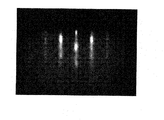
次に、上述のように約450℃の温度で形成した半導体層3をRHEED法により解析したところ、図5に示すように、明瞭なスポット状の回折パターンが観測された。この結果は、基材2の半導体層3の形成面4であるRh(111)面上にAlN(0001)がエピタキシャル成長したことを示している。
Next, when the
また、このRHEED法により得られた回折パターンから、面内のエピタキシャル関係は、格子不整合度が15.7%となるAlN[11−20]//Rh[1−10]であることが導かれる。このように、Rhの六角形の結晶構造上にAlNの六角形の結晶構造が重なって形成されることで、界面エネルギーを低下させて界面反応を防止し、界面反応層が形成されることを防止することができる。 Further, from the diffraction pattern obtained by this RHEED method, it is derived that the in-plane epitaxial relationship is AlN [11-20] // Rh [1-10] with a lattice mismatch degree of 15.7%. It is burned. In this way, the hexagonal crystal structure of AlN is formed on the hexagonal crystal structure of Rh, so that the interfacial reaction is prevented by lowering the interfacial energy and the interfacial reaction layer is formed. Can be prevented.
次に、半導体層3の表面をGIXR(Grazing Incidence X-ray Reflectively:X線反射率)法により解析し、図6に示す結果を得た。この解析結果に論理的フィッティングを掛けたところ、界面反応層が存在しないことを示す結果が得られた。すなわち、この結果は基材2と半導体層3との間に急峻なヘテロ界面を得ることができたことを示している。これは、上述のRHEED法により得られた結果を裏付けるものである。
Next, the surface of the
次に、半導体層3の表面をEBSD(Electron Back Scattering Diffraction:電子線後方散乱回折)法により解析し、図7に示すAlN{11−24}EBSD極点図を得た。この結果は、面内のエピタキシャル関係がAlN[11−20]//Rh[1−10]であることであることを示している。これは、上述のRHEED法の結果を裏付けるものである。また、図7はAlNに30°回転ドメインが存在しない高品質のエピタキシャルな半導体層3が形成されていることを示している。
Next, the surface of the
次に、半導体層3の表面をXPS法により解析したところ、図8に示すようにRh3dピークは観測されず、半導体層3の表面へのRh原子の拡散は見られなかった。この結果は、上述の製造方法によって界面層が生じることなく、高品質の半導体層3が形成されたことを示している。
Next, when the surface of the
一方、上述の方法により形成された半導体層3と比較するため、従来のMOCVD(Metal Organic Chemical Vapor Deposition:有機金属気相成長)法、MBE(Molecular Beam Epitaxy:分子線エピタキシー)法等を想定し、約750℃の温度で基材2の半導体層3の形成面4上にAlNを成長させて半導体層を形成した。そして、形成した半導体層をRHEED法により解析したところ、図9に示すように、リング状のパターンが観測された。この結果は、基材2上に多結晶のAlNが形成されたことを示している。
On the other hand, for comparison with the
また、上述の750℃の温度で形成した半導体層の表面をGIXR法により解析し、図10に示す結果を得た。この測定結果に論理的フィッティングを施したところ、約12nmの界面反応層が存在することを示す結果が得られた。
次いで、650℃の温度で同様に半導体層を形成し、RHEEDにより解析したところ、図5に示すようなスポット状のパターンの上に、図9に示すようなリング状のパターンが重なったパターンが観測された。この結果は、基材2上の半導体層に依然として多結晶のAlNが存在するが、(0001)構造が優位になり始めていることを示している。
Further, the surface of the semiconductor layer formed at the temperature of 750 ° C. was analyzed by the GIXR method, and the result shown in FIG. 10 was obtained. When logical fitting was applied to this measurement result, a result indicating that an interface reaction layer of about 12 nm was present was obtained.
Next, when a semiconductor layer was similarly formed at a temperature of 650 ° C. and analyzed by RHEED, a pattern in which a ring-shaped pattern as shown in FIG. 9 was superimposed on a spot-shaped pattern as shown in FIG. Observed. This result shows that the polycrystalline layer of AlN still exists in the semiconductor layer on the
次いで、350℃および550℃の温度で同様に半導体層を形成し、RHEED法により解析したところ、図5に示すように、明瞭なスポット状のパターンが観測された。この結果は、450℃の温度で半導体層3を形成した場合と同様に、基材2の半導体層の形成面であるRh(111)面上にAlN(0001)がエピタキシャル成長したことを示している。さらに、350℃よりも低い温度で同様に半導体層を形成しRHEED法により解析したところ、図9に示すようなリング状のパターンが測定された。この結果は、350℃よりも低い温度では、基材2上の半導体層は多結晶のAlNによって形成されることを示している。
Next, when semiconductor layers were similarly formed at temperatures of 350 ° C. and 550 ° C. and analyzed by the RHEED method, a clear spot-like pattern was observed as shown in FIG. This result shows that AlN (0001) was epitaxially grown on the Rh (111) surface, which is the formation surface of the semiconductor layer of the
また、上述のように、350℃、450℃、550℃、650℃および750℃の温度で形成した半導体層をそれぞれGIXR法により解析し、それぞれ論理的フィッティングを掛けることにより、図11に示す結果を得た。図11は、約350℃以上かつ550℃以下の温度範囲では、基材2と半導体層との間に界面反応層が形成されることを防止でき、界面反応層が存在しない急峻なヘテロ界面が形成されることを示している。また、550℃よりも高い温度範囲では基材2と半導体層との間に界面反応層が形成されることを示している。
In addition, as described above, the results shown in FIG. 11 are obtained by analyzing the semiconductor layers formed at temperatures of 350 ° C., 450 ° C., 550 ° C., 650 ° C., and 750 ° C. using the GIXR method and applying logical fittings, respectively. Got. FIG. 11 shows that in the temperature range of about 350 ° C. or more and 550 ° C. or less, an interface reaction layer can be prevented from being formed between the
さらに、これらの異なる温度によって形成された半導体層の表面をXPS法により解析し、図12に示す結果を得た。図12に示すように、650℃および750℃の温度で形成された半導体層ではRh3dピークが観測された。このときのRhの表面濃度の推定値はそれぞれ0.1%および0.6%であった。この結果は、基材2と半導体層との間の界面反応により、半導体層にRh原子が拡散したことを示している。
Furthermore, the surface of the semiconductor layer formed at these different temperatures was analyzed by the XPS method, and the results shown in FIG. 12 were obtained. As shown in FIG. 12, Rh3d peaks were observed in the semiconductor layers formed at temperatures of 650 ° C. and 750 ° C. The estimated values of the surface concentration of Rh at this time were 0.1% and 0.6%, respectively. This result shows that Rh atoms diffused into the semiconductor layer due to the interfacial reaction between the
一方、550℃以下の温度ではRh3dピークは観測されず、半導体層表面へのRh原子の拡散は見られなかった。この結果は、550℃以下の温度で半導体層を形成することで、基材と半導体層との間での界面反応を防止し、界面反応層が形成されることを防止でき、基材2と半導体層との間に急峻なヘテロ界面が形成されることを示している。 On the other hand, no Rh3d peak was observed at a temperature of 550 ° C. or lower, and no diffusion of Rh atoms to the semiconductor layer surface was observed. As a result, by forming the semiconductor layer at a temperature of 550 ° C. or less, the interface reaction between the base material and the semiconductor layer can be prevented, and the formation of the interface reaction layer can be prevented. It shows that a steep hetero interface is formed with the semiconductor layer.
また、上述のように450℃の温度で形成した半導体層3を、450℃、550℃、650℃、および750℃の温度で熱処理し、それぞれGIXR法により解析し、論理的フィッティングを掛けることにより、図13に示す結果を得た。図13に示すように、半導体層3が熱処理によって550℃よりも高い温度になっても、基材2と半導体層3との間に界面反応層が形成されることはなく、急峻なヘテロ界面を維持することができる。
Further, the
さらに、これらの熱処理した半導体層3の表面をXPS法により解析し、図14に示す結果を得た。図14に示すように、Rh3dピークは観測されず、約450℃、すなわち350℃以上かつ550℃以下の温度範囲で形成された半導体層は、550℃よりも高い温度での熱処理によっても、Rh原子が半導体層の表面に拡散することがないことを示している。
Furthermore, the surface of these heat-treated
以上説明したように、本実施形態の半導体基板の製造方法によれば、PLD法を用い、350℃以上かつ550℃以下の温度範囲でAlNの半導体層3を形成することで、半導体層3と基材2との間での界面反応を防止し、半導体層3と基材2との間に界面反応層が形成されることを防止できる。したがって、熱伝導性に優れ、紫外線等の短波長の光に対する反射性に優れたRhの基材2上に、界面反応層のない高品質なAlNの半導体層3を形成することができる。
As described above, according to the method for manufacturing a semiconductor substrate of the present embodiment, by using the PLD method, the
また、半導体層3を形成する工程の前に、基材2の半導体層3の形成面4を原子レベルまで平坦化することで、半導体層3の形成面4にAlNの半導体層3をエピタキシャル成長させることができる。これにより、半導体層3の品質を向上させることができる。
また、形成した半導体層3を550℃よりも高い温度で熱処理しても、急峻なヘテロ界面を維持することができ、Rh原子が半導体層3の表面に拡散することがないので、半導体層3上に、さらにGaN等のIII族窒化物の半導体層をエピタキシャル成長させることができる。
In addition, the
Further, even if the formed
〔紫外線発光装置〕
次に、本実施形態の紫外線発光装置について説明する。
図15に示すように、紫外線発光装置10は、上述した半導体基板1の半導体層3上にGaNからなる第二の半導体層5を備えている。AlNからなる半導体層3、GaNからなる半導体層5、および図示しない配線等により、基材2上に紫外線発光素子6が形成されている。
[Ultraviolet light emitting device]
Next, the ultraviolet light emitting device of this embodiment will be described.
As shown in FIG. 15, the ultraviolet
また、本実施形態の別の紫外線発光装置20は、図16に示すように、支持基板7上に上述したRhからなる基材2およびAlNからなる半導体層3が形成され、半導体層3上にGaNからなる第二の半導体層5を備えている。また、図15に示す紫外線発光装置10と同様に、AlNからなる半導体層3、GaNからなる半導体層5、および図示しない配線等により、基材2上に紫外線発光素子6が形成されている。支持基板7としては、例えば、ガラス等の絶縁材料、金属等の導電材料、シリコン等の半導体材料等を用いることができる。
In addition, as shown in FIG. 16, another ultraviolet
上述のように、紫外線発光素子6は紫外線等の短波長の光に対する反射率の高いRhからなる基材2上に形成されているので、紫外線発光素子6によって基材2側に発せられた紫外光を基材2の表面で反射させ、紫外線発光装置10,20の紫外線の取り出し効率を向上させることができる。また、サファイア等の従来の基材と比較して熱伝導率の高いRhからなる基材2によって半導体層3の熱放散を促進し、半導体層3の温度上昇により紫外線発光素子6の性能が低下することを防止することができる。
As described above, since the ultraviolet
尚、この発明は上述した実施の形態に限られるものではなく、本発明の趣旨を逸脱しない範囲で種々変形して実施することができる。例えば、上述の実施形態で説明した半導体基板では、ロジウムからなる基材上に半導体層を形成する場合について説明したが、例えば、金属等の支持基材上にロジウム薄膜を形成し、ロジウム薄膜上に半導体層を形成してもよい。これにより、上述の実施形態と同様の効果が得られる。 The present invention is not limited to the above-described embodiment, and various modifications can be made without departing from the spirit of the present invention. For example, in the semiconductor substrate described in the above-described embodiment, the case where the semiconductor layer is formed on the base material made of rhodium has been described. For example, a rhodium thin film is formed on a support base material such as metal, and the rhodium thin film is formed. A semiconductor layer may be formed. Thereby, the same effect as the above-mentioned embodiment is acquired.
また、基材上に350℃以上かつ550℃以下の温度でIII族窒化物の半導体層をエピタキシャル成長させる方法として、PLD法以外の方法を用いてもよい。PLD法以外の方法としては、PED(Pulsed Electron Deposition:パルス電子線堆積)法またはスパッタリング法等、高いエネルギーでIII族窒化物を蒸着させる方法を用いることで、上述の温度範囲で基材上にIII族窒化物の半導体層をエピタキシャル成長させることができる。 Further, as a method for epitaxially growing a group III nitride semiconductor layer on the substrate at a temperature of 350 ° C. or higher and 550 ° C. or lower, a method other than the PLD method may be used. As a method other than the PLD method, a method of depositing a group III nitride with high energy, such as a PED (Pulsed Electron Deposition) method or a sputtering method, is used on the substrate in the above temperature range. A group III nitride semiconductor layer can be epitaxially grown.
1 半導体基板
2 基材
3 半導体層
4 形成面
5 半導体層
6 紫外線発光素子
10 紫外線発光装置
20 紫外線発光装置
DESCRIPTION OF
Claims (13)
InXGaYAl1−X−YN(0≦X≦1、0≦Y≦1、0≦X+Y≦1)…(I) The semiconductor substrate according to claim 1, wherein the group III nitride includes at least one of In, Ga, and Al and is represented by the following chemical formula (I).
In X Ga Y Al 1-X -Y N (0 ≦ X ≦ 1,0 ≦ Y ≦ 1,0 ≦ X + Y ≦ 1) ... (I)
Priority Applications (1)
| Application Number | Priority Date | Filing Date | Title |
|---|---|---|---|
| JP2007079117A JP2008243934A (en) | 2007-03-26 | 2007-03-26 | Semiconductor substrate, method for manufacturing the same, and ultraviolet light emitting device |
Applications Claiming Priority (1)
| Application Number | Priority Date | Filing Date | Title |
|---|---|---|---|
| JP2007079117A JP2008243934A (en) | 2007-03-26 | 2007-03-26 | Semiconductor substrate, method for manufacturing the same, and ultraviolet light emitting device |
Publications (1)
| Publication Number | Publication Date |
|---|---|
| JP2008243934A true JP2008243934A (en) | 2008-10-09 |
Family
ID=39914950
Family Applications (1)
| Application Number | Title | Priority Date | Filing Date |
|---|---|---|---|
| JP2007079117A Pending JP2008243934A (en) | 2007-03-26 | 2007-03-26 | Semiconductor substrate, method for manufacturing the same, and ultraviolet light emitting device |
Country Status (1)
| Country | Link |
|---|---|
| JP (1) | JP2008243934A (en) |
Citations (8)
| Publication number | Priority date | Publication date | Assignee | Title |
|---|---|---|---|---|
| JPH11260835A (en) * | 1997-07-11 | 1999-09-24 | Tdk Corp | Substrates for electronic devices |
| JP2001284266A (en) * | 2000-03-31 | 2001-10-12 | Toyoda Gosei Co Ltd | Method of manufacturing group III nitride compound semiconductor and group III nitride compound semiconductor device |
| JP2004063834A (en) * | 2002-07-30 | 2004-02-26 | Japan Science & Technology Corp | Method for forming single crystal thin film on electromagnetic steel substrate, and single-crystal thin-film device therefor |
| JP2004269313A (en) * | 2003-03-07 | 2004-09-30 | Hitachi Cable Ltd | Manufacturing method of gallium nitride crystal substrate |
| JP2005332877A (en) * | 2004-05-18 | 2005-12-02 | Rohm Co Ltd | Light emitting diode element and its manufacturing method |
| JP2006190963A (en) * | 2004-12-30 | 2006-07-20 | Ind Technol Res Inst | Light emitting diode and structure thereof |
| JP2006253500A (en) * | 2005-03-11 | 2006-09-21 | Kanagawa Acad Of Sci & Technol | Method for removing oxygen from solid surface, crystal growth method, semiconductor manufacturing method, and semiconductor device |
| JP2006260578A (en) * | 2006-03-23 | 2006-09-28 | Nissan Motor Co Ltd | Device for monitoring periphery of vehicle |
-
2007
- 2007-03-26 JP JP2007079117A patent/JP2008243934A/en active Pending
Patent Citations (8)
| Publication number | Priority date | Publication date | Assignee | Title |
|---|---|---|---|---|
| JPH11260835A (en) * | 1997-07-11 | 1999-09-24 | Tdk Corp | Substrates for electronic devices |
| JP2001284266A (en) * | 2000-03-31 | 2001-10-12 | Toyoda Gosei Co Ltd | Method of manufacturing group III nitride compound semiconductor and group III nitride compound semiconductor device |
| JP2004063834A (en) * | 2002-07-30 | 2004-02-26 | Japan Science & Technology Corp | Method for forming single crystal thin film on electromagnetic steel substrate, and single-crystal thin-film device therefor |
| JP2004269313A (en) * | 2003-03-07 | 2004-09-30 | Hitachi Cable Ltd | Manufacturing method of gallium nitride crystal substrate |
| JP2005332877A (en) * | 2004-05-18 | 2005-12-02 | Rohm Co Ltd | Light emitting diode element and its manufacturing method |
| JP2006190963A (en) * | 2004-12-30 | 2006-07-20 | Ind Technol Res Inst | Light emitting diode and structure thereof |
| JP2006253500A (en) * | 2005-03-11 | 2006-09-21 | Kanagawa Acad Of Sci & Technol | Method for removing oxygen from solid surface, crystal growth method, semiconductor manufacturing method, and semiconductor device |
| JP2006260578A (en) * | 2006-03-23 | 2006-09-28 | Nissan Motor Co Ltd | Device for monitoring periphery of vehicle |
Similar Documents
| Publication | Publication Date | Title |
|---|---|---|
| US8101498B2 (en) | Bonded intermediate substrate and method of making same | |
| US7732301B1 (en) | Bonded intermediate substrate and method of making same | |
| JP5312797B2 (en) | Method for producing optoelectronic substrate | |
| TWI477666B (en) | Method for preparing epitaxial structure with microstructure | |
| TWI426620B (en) | Method for producing group III-V nitride semiconductor and method for manufacturing light-emitting element | |
| US20110117726A1 (en) | Bonded intermediate substrate and method of making same | |
| JP2003249453A (en) | Manufacturing method for gallium nitride substrate | |
| FR2908925A1 (en) | METHOD FOR INTEGRATING A III-N TYPE COMPONENT, SUCH AS GAS, ON A NOMINAL SILICON (001) SUBSTRATE | |
| JP4996448B2 (en) | Method for creating a semiconductor substrate | |
| TWI458672B (en) | Epitaxial structure with microstructure | |
| CN112151645A (en) | Preparation of large-angle oblique-cutting sapphire substrate AlN, light-emitting diode and preparation method thereof | |
| CN103378235B (en) | Light-emitting diode | |
| JP2014031300A (en) | Gallium oxide substrate and manufacturing method of the same | |
| TW201241876A (en) | A epitaxialstructure and method for making the same | |
| US11162188B2 (en) | Method for producing a crystalline layer in a III-N compound by van der Waals epitaxy from graphene | |
| WO2006057422A1 (en) | Semiconductor multilayer substrate, method for producing same and light-emitting device | |
| KR100959290B1 (en) | Nitride semiconductor and manufacturing method thereof | |
| JP5439526B2 (en) | Group III nitride semiconductor and substrate for group III nitride semiconductor growth | |
| CN108231545A (en) | It is grown in InN nano-pillar epitaxial wafers on copper foil substrate and preparation method thereof | |
| JP2009221083A (en) | Group iii nitride semiconductor and method for manufacturing the same | |
| JP2008053372A (en) | Manufacturing method of semiconductor device | |
| JP2008243934A (en) | Semiconductor substrate, method for manufacturing the same, and ultraviolet light emitting device | |
| JP4786587B2 (en) | Group III nitride semiconductor and method for manufacturing the same, substrate for manufacturing group III nitride semiconductor | |
| JP2007123858A (en) | Method for producing group 3-5 nitride semiconductor | |
| JP2010251743A (en) | Group III nitride semiconductor growth substrate, group III nitride semiconductor free-standing substrate, group III nitride semiconductor device, and methods of manufacturing the same |
Legal Events
| Date | Code | Title | Description |
|---|---|---|---|
| A621 | Written request for application examination |
Free format text: JAPANESE INTERMEDIATE CODE: A621 Effective date: 20100203 |
|
| A977 | Report on retrieval |
Free format text: JAPANESE INTERMEDIATE CODE: A971007 Effective date: 20110921 |
|
| A131 | Notification of reasons for refusal |
Free format text: JAPANESE INTERMEDIATE CODE: A131 Effective date: 20120131 |
|
| A02 | Decision of refusal |
Free format text: JAPANESE INTERMEDIATE CODE: A02 Effective date: 20120605 |