JP2008153685A - Manufacturing method of semiconductor device - Google Patents
Manufacturing method of semiconductor device Download PDFInfo
- Publication number
- JP2008153685A JP2008153685A JP2008023939A JP2008023939A JP2008153685A JP 2008153685 A JP2008153685 A JP 2008153685A JP 2008023939 A JP2008023939 A JP 2008023939A JP 2008023939 A JP2008023939 A JP 2008023939A JP 2008153685 A JP2008153685 A JP 2008153685A
- Authority
- JP
- Japan
- Prior art keywords
- trench
- groove
- trench groove
- semiconductor substrate
- manufacturing
- Prior art date
- Legal status (The legal status is an assumption and is not a legal conclusion. Google has not performed a legal analysis and makes no representation as to the accuracy of the status listed.)
- Pending
Links
Images


Classifications
-
- H—ELECTRICITY
- H10—SEMICONDUCTOR DEVICES; ELECTRIC SOLID-STATE DEVICES NOT OTHERWISE PROVIDED FOR
- H10D—INORGANIC ELECTRIC SEMICONDUCTOR DEVICES
- H10D62/00—Semiconductor bodies, or regions thereof, of devices having potential barriers
- H10D62/10—Shapes, relative sizes or dispositions of the regions of the semiconductor bodies; Shapes of the semiconductor bodies
- H10D62/13—Semiconductor regions connected to electrodes carrying current to be rectified, amplified or switched, e.g. source or drain regions
- H10D62/149—Source or drain regions of field-effect devices
- H10D62/151—Source or drain regions of field-effect devices of IGFETs
-
- H—ELECTRICITY
- H10—SEMICONDUCTOR DEVICES; ELECTRIC SOLID-STATE DEVICES NOT OTHERWISE PROVIDED FOR
- H10D—INORGANIC ELECTRIC SEMICONDUCTOR DEVICES
- H10D30/00—Field-effect transistors [FET]
- H10D30/01—Manufacture or treatment
- H10D30/021—Manufacture or treatment of FETs having insulated gates [IGFET]
- H10D30/0221—Manufacture or treatment of FETs having insulated gates [IGFET] having asymmetry in the channel direction, e.g. lateral high-voltage MISFETs having drain offset region or extended-drain MOSFETs [EDMOS]
-
- H—ELECTRICITY
- H10—SEMICONDUCTOR DEVICES; ELECTRIC SOLID-STATE DEVICES NOT OTHERWISE PROVIDED FOR
- H10D—INORGANIC ELECTRIC SEMICONDUCTOR DEVICES
- H10D30/00—Field-effect transistors [FET]
- H10D30/60—Insulated-gate field-effect transistors [IGFET]
- H10D30/601—Insulated-gate field-effect transistors [IGFET] having lightly-doped drain or source extensions, e.g. LDD IGFETs or DDD IGFETs
- H10D30/603—Insulated-gate field-effect transistors [IGFET] having lightly-doped drain or source extensions, e.g. LDD IGFETs or DDD IGFETs having asymmetry in the channel direction, e.g. lateral high-voltage MISFETs having drain offset region or extended drain IGFETs [EDMOS]
-
- H—ELECTRICITY
- H10—SEMICONDUCTOR DEVICES; ELECTRIC SOLID-STATE DEVICES NOT OTHERWISE PROVIDED FOR
- H10D—INORGANIC ELECTRIC SEMICONDUCTOR DEVICES
- H10D62/00—Semiconductor bodies, or regions thereof, of devices having potential barriers
- H10D62/10—Shapes, relative sizes or dispositions of the regions of the semiconductor bodies; Shapes of the semiconductor bodies
- H10D62/113—Isolations within a component, i.e. internal isolations
- H10D62/115—Dielectric isolations, e.g. air gaps
- H10D62/116—Dielectric isolations, e.g. air gaps adjoining the input or output regions of field-effect devices, e.g. adjoining source or drain regions
-
- H—ELECTRICITY
- H10—SEMICONDUCTOR DEVICES; ELECTRIC SOLID-STATE DEVICES NOT OTHERWISE PROVIDED FOR
- H10D—INORGANIC ELECTRIC SEMICONDUCTOR DEVICES
- H10D62/00—Semiconductor bodies, or regions thereof, of devices having potential barriers
- H10D62/10—Shapes, relative sizes or dispositions of the regions of the semiconductor bodies; Shapes of the semiconductor bodies
- H10D62/13—Semiconductor regions connected to electrodes carrying current to be rectified, amplified or switched, e.g. source or drain regions
- H10D62/149—Source or drain regions of field-effect devices
- H10D62/151—Source or drain regions of field-effect devices of IGFETs
- H10D62/156—Drain regions of DMOS transistors
-
- H10P30/222—
Landscapes
- Insulated Gate Type Field-Effect Transistor (AREA)
Abstract
【課題】 トレンチ溝の周囲にオフセットドレイン領域を有する横型高耐圧トレンチMOSFETを製造するため、トレンチ溝の周囲に最適な濃度の不純物を注入し、また幅の広いトレンチ溝内を酸化膜で埋めること。
【解決手段】 トレンチ溝2の周囲にオフセットドレイン領域3を形成するにあたり、トレンチ内面にドープドポリシリコン膜24を形成し、ドライブおこないトレンチ溝の側面および底面に拡散する。その後、ドープドポリシリコン膜24を熱酸化する。その後トレンチ溝内を酸化膜で埋めるにあたり、熱酸化によりトレンチ溝2内を酸化物4で埋めるか、熱酸化によりトレンチ溝内に酸化膜を生成して溝を狭めた後、残った溝を酸化物の堆積により埋める。あるいは、複数のトレンチ溝を形成し、それらの中を酸化物で埋めると共に、トレンチ間の基板部分を熱酸化して酸化膜に変える。
【選択図】 図1To manufacture a lateral high breakdown voltage trench MOSFET having an offset drain region around a trench groove, an impurity having an optimum concentration is implanted around the trench groove, and the wide trench groove is filled with an oxide film. .
In forming an offset drain region 3 around a trench groove 2, a doped polysilicon film 24 is formed on the inner surface of the trench and is driven and diffused on the side and bottom surfaces of the trench groove. Thereafter, the doped polysilicon film 24 is thermally oxidized. Then, when filling the trench groove with an oxide film, the trench groove 2 is filled with oxide 4 by thermal oxidation, or an oxide film is formed in the trench groove by thermal oxidation to narrow the groove, and the remaining groove is oxidized. It is buried by the accumulation of things. Alternatively, a plurality of trench grooves are formed and filled with oxide, and the substrate portion between the trenches is thermally oxidized to be changed into an oxide film.
[Selection] Figure 1
Description
本発明は、トレンチ構造を有する半導体装置の製造方法に関し、特にパワーICなどに使用される横型高耐圧トレンチMOSFETを構成する半導体装置の製造方法に関し、特にトレンチ部にオフセットドレイン領域おW計性するプロセスにおいて、最適な拡散方法、トレンチ内の絶縁膜の埋め込み方法に関する。 The present invention relates to a method for manufacturing a semiconductor device having a trench structure, and more particularly to a method for manufacturing a semiconductor device constituting a lateral high voltage trench MOSFET used in a power IC or the like, and more particularly to an offset drain region in a trench portion. The present invention relates to an optimum diffusion method and a method for filling an insulating film in a trench.
従来よりトレンチ技術は、DRAMなどにおいてキャパシタンスを作製する技術や素子分離のためのSOI技術として、またディスクリートMOSFETのトレンチゲート技術として、種々検討されている。また、近年、パワーICなどに使用される横型高耐圧MOSFETにおいてもトレンチ技術を応用する提案がなされている。横型高耐圧MOSFETの構造の一つに、トレンチ溝の周囲にオフセットドレイン領域を設けたものがある。このようにトレンチ溝の周囲にオフセットドレイン領域を設けるためには、トレンチ溝の周囲に最適な濃度の不純物イオンを注入する技術と、幅の広いトレンチ溝内に酸化膜などを埋め込む技術が必要である。 Conventionally, various trench techniques have been studied as a technique for producing a capacitance in a DRAM or the like, an SOI technique for element isolation, and a trench gate technique for a discrete MOSFET. In recent years, proposals have also been made to apply trench technology to lateral high voltage MOSFETs used in power ICs and the like. One of the structures of a lateral high voltage MOSFET is one in which an offset drain region is provided around a trench groove. In order to provide the offset drain region around the trench groove in this way, a technique for implanting impurity ions at an optimum concentration around the trench groove and a technique for embedding an oxide film or the like in the wide trench groove are required. is there.
しかしながら、トレンチ溝の周囲にオフセットドレイン領域を設けるためのイオン注入技術や、トレンチ溝を酸化膜などで埋める技術に関して、実現上有効な提案や報告はほとんどない。
本発明は、上記事情に鑑みてなされたものであって、トレンチ溝の周囲にオフセットドレイン領域を有する横型高耐圧トレンチMOSFETを得るために、トレンチ溝の周囲に最適な濃度の不純物イオンを拡散する方法、および幅の広いトレンチ溝内を酸化膜で埋める方法を含む半導体装置の製造方法を提供することを目的とする。
However, there are almost no proposals or reports effective in terms of ion implantation technology for providing an offset drain region around the trench groove and technology for filling the trench groove with an oxide film or the like.
The present invention has been made in view of the above circumstances, and in order to obtain a lateral high breakdown voltage trench MOSFET having an offset drain region around a trench groove, impurity ions having an optimum concentration are diffused around the trench groove. It is an object of the present invention to provide a method of manufacturing a semiconductor device including a method and a method of filling a wide trench with an oxide film.
上記目的を達成するため、本発明にかかる半導体装置の製造方法は、トレンチ溝の周囲にオフセットドレイン領域を形成するにあたって、トレンチ溝を形成した後、該トレンチ溝内にドレイン領域と同導電型の導電膜を堆積し、その後ドライブ処理を行うことにより、該導電膜より含有不純物がトレンチ側面、底面へ固相拡散し、オフセットドレイン領域を形成する。
この発明によれば、トレンチの底面および側面に制御性よく拡散層を形成することができる。また、トレンチ内に堆積する導電膜の濃度,厚さ,ドライブ時間などを制御することにより、オフセットドレイン領域の濃度を最適に制御できる。
また、上記目的を達成するため、本発明にかかる半導体装置の製造方法は、トレンチ溝内を酸化膜で埋めるにあたって、トレンチ溝を形成した後、そのトレンチ溝の幅が、半導体基板の熱酸化により生成される酸化膜によって埋めることができる程度である場合には、その熱酸化膜でトレンチ溝内を埋める。一方、トレンチ溝の幅が、半導体基板の熱酸化により生成される酸化膜だけでは埋めきれない程度である場合には、まず熱酸化膜によりトレンチ溝の幅を狭め、残った溝に酸化物を堆積させて溝を埋める。また、複数のトレンチ溝を、半導体基板の熱酸化により生成される酸化膜の厚さに相当する距離だけ離して形成し、各トレンチ内を熱酸化膜や酸化物の堆積により埋めるとともに、熱酸化によって各トレンチ間の半導体部分を酸化膜に変える。
In order to achieve the above object, in a method of manufacturing a semiconductor device according to the present invention, in forming an offset drain region around a trench groove, after forming the trench groove, the same conductivity type as the drain region is formed in the trench groove. By depositing a conductive film and then performing a drive process, impurities contained from the conductive film are solid-phase diffused to the side and bottom surfaces of the trench, thereby forming an offset drain region.
According to the present invention, the diffusion layer can be formed with good controllability on the bottom and side surfaces of the trench. Further, the concentration of the offset drain region can be optimally controlled by controlling the concentration, thickness, drive time and the like of the conductive film deposited in the trench.
Further, in order to achieve the above object, in the method of manufacturing a semiconductor device according to the present invention, in filling the trench groove with an oxide film, after forming the trench groove, the width of the trench groove is caused by thermal oxidation of the semiconductor substrate. If the oxide film can be filled with the oxide film, the trench groove is filled with the thermal oxide film. On the other hand, when the width of the trench groove is such that it cannot be filled with only the oxide film generated by thermal oxidation of the semiconductor substrate, the width of the trench groove is first narrowed by the thermal oxide film, and the oxide is added to the remaining groove. Deposit to fill the trench. In addition, a plurality of trench grooves are formed apart by a distance corresponding to the thickness of the oxide film generated by thermal oxidation of the semiconductor substrate, and each trench is filled with thermal oxide film or oxide deposition, and thermal oxidation is performed. Thus, the semiconductor portion between the trenches is changed to an oxide film.
この発明によれば、トレンチ溝の幅が、熱酸化膜によって埋めることができる程度である場合には、熱酸化をおこなうだけでトレンチ溝内が酸化膜で埋まる。一方、トレンチ溝の幅が、熱酸化膜によって埋めることができる程度よりも広い場合には、熱酸化をおこなった後に酸化物を堆積させることにより、トレンチ溝内が酸化膜(酸化物)で埋まる。また、複数のトレンチ溝内を酸化膜(酸化物)で埋めるとともに、複数のトレンチ溝同士の間を熱酸化により酸化膜に変えることによって、複数のトレンチ溝に渡る幅の広いトレンチ溝内が酸化膜(酸化物)で埋められたことになる。 According to the present invention, when the width of the trench groove is such that it can be filled with the thermal oxide film, the trench groove is filled with the oxide film only by performing thermal oxidation. On the other hand, when the width of the trench groove is wider than that which can be filled with the thermal oxide film, the trench groove is filled with the oxide film (oxide) by depositing oxide after thermal oxidation. . In addition, the trenches are filled with oxide films (oxides), and the trenches between the trenches are changed to oxide films by thermal oxidation, thereby oxidizing the wide trenches across the trenches. It is filled with a film (oxide).
本発明によれば、トレンチ溝の側面および底面に沿う部分の不純物濃度最適に制御することができるので、たとえば数百ボルト程度の高耐圧MOSFETのオフセットドレイン濃度をイオン注入により最適化することができる。また、幅の広いトレンチ溝内を酸化物で埋めることができるので、容易に高耐圧化することができる。したがって、たとえば数百ボルトクラスの横型MOSFETが得られる。 According to the present invention, the impurity concentration in the portion along the side surface and the bottom surface of the trench groove can be optimally controlled, so that the offset drain concentration of a high breakdown voltage MOSFET of, for example, about several hundred volts can be optimized by ion implantation. . Further, since the inside of the wide trench can be filled with an oxide, a high breakdown voltage can be easily achieved. Therefore, for example, a lateral MOSFET of several hundred volts class can be obtained.
以下に、本発明の実施の形態にかかる半導体装置の製造方法について図面を参照しつつ詳細に説明する。
実施の形態1.
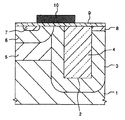
図1は、本発明にかかる半導体装置の製造方法により製造される半導体装置の一例を示す縦断面図である。この半導体装置は、P型の半導体基板1、トレンチ2、N-オフセットドレイン領域3、トレンチ2内を埋める酸化物4、Pウェル領域5、Pベース領域6、N+ソース領域7、N+ドレイン領域8、ゲート酸化膜9、ゲート電極10、層間絶縁膜11、ソース電極12、ドレイン電極13およびパッシベーション膜14を備えており、横型トレンチMOSFETを構成する。
トレンチ2は、半導体基板1の表面部分において、その表面から形成されており、酸化物4で埋められている。N-オフセットドレイン領域3はトレンチ2の周囲、すなわち側面および底面を囲むように形成されている。Pウェル領域5は、半導体基板1の、トレンチ2に対してソース側の表面部分において、N-オフセットドレイン領域3の外側に隣接して形成されている。Pベース領域6はPウェル領域5の表面部分に形成されている。N+ソース領域7は、Pベース領域6の表面部分において、N-オフセットドレイン領域3から離れて形成されている。
Hereinafter, a semiconductor device manufacturing method according to an embodiment of the present invention will be described in detail with reference to the drawings.
FIG. 1 is a longitudinal sectional view showing an example of a semiconductor device manufactured by the method for manufacturing a semiconductor device according to the present invention. The semiconductor device includes a P-
The
N+ドレイン領域8は、N-オフセットドレイン領域3の、トレンチ2に対してドレイン側(ソース側の反対側)の表面部分に形成されている。ゲート酸化膜9はN+ソース領域7からN-オフセットドレイン領域3のソース側部分に至る表面上に形成されている。ゲート電極10はゲート酸化膜9上に形成されている。層間絶縁膜11はゲート電極10およびトレンチ2の上部を覆っている。ソース電極12はPベース領域6およびN+ソース領域7に電気的に接続している。ドレイン電極13はN+ドレイン領域8に電気的に接続している。パッシベーション膜14は半導体装置全体を被覆している。
つぎに、図1に示す構成の半導体装置の製造プロセスについて説明する。図2〜図13は、その製造プロセスを説明するための図であり、半導体装置の製造途中の段階における構造を順に示す縦断面図である。まず、P型の半導体基板1を酸化してその表面にたとえば300オングストロームの厚さの酸化膜21を形成する。つづいて、その酸化膜21の上に窒化膜22をたとえば1000オングストロームの厚さで堆積させる(図2参照)。さらに、窒化膜22の上にレジスト23を塗布し(図3参照)、露光、現像をおこなってレジスト23の、トレンチ2の形成領域上の部分を除去する(図4参照)。残留したレジスト23をマスクにしてエッチングをおこない、窒化膜22および酸化膜21の、トレンチ2の形成領域上の部分を除去して、基板表面の、トレンチ2の形成領域を露出させる(図5参照)。その後、レジスト灰化によりレジスト23を除去する(図6参照)。
The N + drain region 8 is formed in the surface portion of the N −
Next, a manufacturing process of the semiconductor device having the configuration shown in FIG. 1 will be described. 2 to 13 are views for explaining the manufacturing process, and are longitudinal cross-sectional views sequentially showing structures in the middle of manufacturing the semiconductor device. First, the P-
ついで、基板表面に残留した窒化膜22および酸化膜21をマスクにしてシリコンエッチングをおこない、たとえば幅が5μmで深さが20μmのトレンチ溝2を基板表面に対して垂直に形成する(図7参照)。しかる後、基板表面に対して斜めの方向からリンイオンを注入する(図8参照)。このときのイオン注入量はたとえば8×1012cm-2である。また、イオン注入方向と基板表面の法線方向(すなわちトレンチ溝2の側面)とのなす角はおおよそ14°である。イオン注入方向と基板表面の法線方向とのなす角が決まったら、基板を回転させながらイオン注入をおこなう。こうすることにより、トレンチ溝の側面全域にイオン注入することができる。
ここで、斜めイオン注入において、イオン注入方向と基板表面の法線方向とのなす角度は、トレンチ溝2の幅および深さをそれぞれWおよびLとすると、tan-1(W/L)で決まる。この角度でイオン打ち込みをおこなうことによって、半導体基板1の、トレンチ溝2の側面に沿う部分にのみリンイオンが注入される。これは、イオンの打ち込み方向から見て、トレンチ溝2の底面はトレンチ溝2の周囲の基板部分により影になり、リンイオンが到達しないが、トレンチ溝2の側面は影にならないからである。したがって、トレンチ溝2の幅および深さが変わると、それに対応して斜めイオン注入の注入角度も変わることになる。
Next, silicon etching is performed using the
Here, in oblique ion implantation, the angle formed by the ion implantation direction and the normal direction of the substrate surface is determined by tan −1 (W / L), where the width and depth of the
ついで、基板表面に対して垂直な方向、すなわちトレンチ溝2の側面に対して0°の方向からリンイオンを注入する(図9参照)。この0°イオン注入では、トレンチ溝2の底面に沿う部分にのみリンイオンが注入される(図10参照)。ここで、N-オフセットドレイン領域3の、トレンチ溝2の側面に沿う部分と底面に沿う部分とでリンイオンの表面濃度を同一にするため、底面へのイオン注入量を側面へのイオン注入量の5μm/20μm倍とする。つまり、0°イオン注入時のイオン注入量はたとえば2×1012cm-2である。また、先の斜めイオン注入では、トレンチ溝2の底面に沿う部分にリンイオンが注入されないため、トレンチ溝2の底面に沿う部分に局部的なリンイオンの高濃度領域が形成されることはない。
ついで、酸化・ドライブをおこない、拡散深さxjがたとえば6μm程度となるようにドライブさせる。これによって、N-オフセットドレイン領域3ができあがる。また、このとき同時に、トレンチ溝2の側面および底面には熱酸化膜が生成する。この熱酸化膜の厚さはたとえば4μm程度である。したがって、トレンチ溝2内はこの熱酸化膜よりなる酸化物4によって埋められる(図11参照)。なお、図11において、酸化物4内の深さ方向に延びる点線は、トレンチ溝2の両側面および底面から成長した熱酸化膜が出会って一体化したときの境界を仮想的に示している。
Next, phosphorus ions are implanted from a direction perpendicular to the substrate surface, that is, a direction of 0 ° with respect to the side surface of the trench 2 (see FIG. 9). In this 0 ° ion implantation, phosphorus ions are implanted only into the portion along the bottom surface of the trench groove 2 (see FIG. 10). Here, in order to make the surface concentration of phosphorus ions the same in the portion along the side surface of the
Next, oxidation and driving are performed to drive the diffusion depth xj to be about 6 μm, for example. As a result, the N − offset
ついで、基板表面の窒化膜22および酸化膜21を除去し(図12参照)、Pウェル領域5、Pベース領域6、N+ソース領域7、N+ドレイン領域8、ゲート酸化膜9およびゲート電極10を周知の方法により形成する(図13参照)。そして、層間絶縁膜11、ソース電極12、ドレイン電極13およびパッシベーション膜14を形成して、図1に示す構成の横型トレンチMOSFETができあがる。
上述した実施の形態1によれば、N-オフセットドレイン領域3の、トレンチ溝2の側面に沿う部分と、底面に沿う部分とに別々にイオン注入をおこなうので、それぞれの部分の不純物濃度を最適に制御することができる。また、トレンチ溝2内を酸化物4で埋めることができる。したがって、たとえば耐圧が数百ボルト程度の横型高耐圧トレンチMOSFETが得られる。また、耐圧と単位面積当たりのオン抵抗のトレードオフを改善することができる。
なお、N-オフセットドレイン領域3の、トレンチ溝2の側面に沿う部分には、N-オフセットドレイン領域3と逆の導電型で、かつ半導体基板1よりも不純物濃度が高いPウェル領域5およびPベース領域6が形成されているため、N-オフセットドレイン領域3の、トレンチ溝2の側面に沿う部分の不純物濃度を、底面に沿う部分の不純物濃度よりも高くすることができる。また、トレンチ溝2内にフィールドプレートを形成する場合にも、トレンチ溝2の側面に沿う部分の不純物濃度を、底面に沿う部分の不純物濃度よりも高くすることができる。このようにすれば、デバイスの耐圧と単位面積当たりのオン抵抗のトレードオフを改善することができる。
Next, the
According to the first embodiment described above, since the ion implantation is separately performed in the portion along the side surface of the
Note that in the portion of the N − offset
実施の形態2.
図14〜図16は、図1と同様の構成の半導体装置を製造するプロセスの他の例を説明するための図であり、半導体装置の製造途中の段階における構造を順に示す縦断面図である。半導体基板1にトレンチ溝2を形成するまで(図2〜図7参照)とトレンチ内に酸化膜を埋めた後(図12〜図13)は実施の形態1と同じである。
トレンチ形成後、減圧CVDにより、シランおよびリンドープ用にホスフィンを用いて、リン(P31)濃度1×1020cm-3程度のドープドポリシリコン膜24を300オングストローム堆積し(図14)、その後1150℃で120分間ドライブをおこなう。すると、ドープドポリシリコン膜24中のリンがトレンチ側面および底面に拡散し(固相拡散)、深さ3μm,ピーク濃度1×1016cm-3のN型不純物拡散層3が形成される(図15)。その後基板を加熱して、ドープドポリシリコン膜24を熱酸化膜とする。さらに酸化を継続してトレンチ内部を熱酸化膜で埋める(図16)。その後半導体基板1の表面のドープドポリシリコン膜24が酸化された膜、窒化膜22および酸化膜21を除去すると図12のようになる。
上述した実施の形態2によれば、トレンチの側面および底面の制御性よく拡散領域を形成することができる。
14 to 16 are views for explaining another example of the process for manufacturing the semiconductor device having the same configuration as that in FIG. 1, and are longitudinal sectional views sequentially showing the structure in the course of manufacturing the semiconductor device. . The process is the same as that of the first embodiment until the
After the trench formation, a doped
According to the second embodiment described above, the diffusion regions can be formed with good controllability on the side and bottom surfaces of the trench.
実施の形態3.
図17〜図20は、図1と同様の構成の半導体装置を製造するプロセスの他の例を説明するための図であり、半導体装置の製造途中の段階における構造を順に示す縦断面図である。半導体基板1にトレンチ溝2を形成し、斜めイオン注入および0°イオン注入をおこなうまで(図2〜図10参照)、または、半導体基板1にトレンチ溝2を形成し、ドープドポリシリコン層24を形成し、ドライブをおこなうまでは、実施の形態1または実施の形態2と同じである。ただし、ここではトレンチ溝2の幅および深さをそれぞれたとえば7μmおよび20μmとする。このときの斜めイオン注入におけるイオン注入方向と基板表面の法線方向とのなす角はおおよそ19°である。なお、実施の形態1、2と同じ構成については実施の形態1、2と同一の符号を付す。
実施の形態1の場合は、イオン注入後、トレンチ溝2の側面および底面に厚さ2μmの熱酸化膜が生成するように、酸化・ドライブをおこなう。これによって、N-オフセットドレイン領域3ができるとともに、トレンチ溝2の側面および底面に厚さ2μmの熱酸化膜31が生成する。このとき、トレンチ溝2は熱酸化膜31によっては完全に埋まらず、トレンチ溝2の中央には、幅が4μm程度の溝32が残る。つまり、トレンチ溝2の幅が狭まったことになる(図17参照)。実施の形態2の場合は、熱酸化によりドープドポリシリコン膜24を酸化し、窒化膜22の上および側面に形成されている該ドープドポリシリコン膜24を酸化した酸化膜を除去する(図17参照)。
17 to 20 are views for explaining another example of the process for manufacturing the semiconductor device having the same configuration as that in FIG. 1, and are longitudinal sectional views sequentially showing the structure in the course of manufacturing the semiconductor device. . Until
In the case of the first embodiment, after ion implantation, oxidation and drive are performed so that a thermal oxide film having a thickness of 2 μm is formed on the side surface and bottom surface of
ついで、基板表面の窒化膜22および酸化膜21を除去し(図18参照)、基板表面にTEOSやHTOなどの酸化膜33を堆積させて、残った溝32を埋める(図19参照)。しかる後、溝32内にのみ酸化膜33が残るように、基板表面上の酸化膜33を除去する(図20参照)。そして、図示省略するが、Pウェル領域5、Pベース領域6、N+ソース領域7、N+ドレイン領域8、ゲート酸化膜9、ゲート電極10、層間絶縁膜11、ソース電極12、ドレイン電極13およびパッシベーション膜14を形成して、図1と同様の構成の横型トレンチMOSFETができあがる。
上述した実施の形態3によれば、実施の形態1,2と同様に、たとえば耐圧が数百ボルト程度の横型高耐圧トレンチMOSFETが得られるという効果に加えて、実施の形態1,2よりも幅が広いトレンチ溝2に酸化膜31および酸化物33を埋め込むことができるという効果が得られる。
実施の形態4.
図21〜図23は、図1と同様の構成の半導体装置を製造するプロセスのさらに他の例を説明するための図であり、半導体装置の製造途中の段階における構造を順に示す縦断面図である。半導体基板1にトレンチ溝2を形成し、斜めイオン注入および0°イオン注入をおこなうまで(図2〜図9、図21参照)は実施の形態1と同じである。ただし、ここでは複数、たとえば2個のトレンチ溝41,42を、幅が2μmの半導体基板部分43を挟んで形成する。トレンチ溝41,42は、実施の形態1のトレンチ溝2と同じである。すなわち、トレンチ溝41,42の幅はたとえば5μmであり、深さはたとえば20μmである。なお、実施の形態1と同じ構成については実施の形態1と同一の符号を付す。
Next, the
According to the third embodiment described above, as in the first and second embodiments, in addition to the effect of obtaining a lateral high breakdown voltage trench MOSFET having a breakdown voltage of about several hundred volts, for example, it is more than the first and second embodiments. An effect is obtained that the
FIGS. 21 to 23 are diagrams for explaining still another example of the process for manufacturing the semiconductor device having the same configuration as that in FIG. 1, and are longitudinal sectional views sequentially showing the structure in the course of manufacturing the semiconductor device. is there. The process until the
イオン注入後、トレンチ溝41,42の側面および底面に厚さ4μmの熱酸化膜が生成するように、酸化・ドライブをおこなう。これによって、トレンチ溝41,42内は厚さ4μmの熱酸化膜で完全に埋められるとともに、トレンチ溝41とトレンチ42との間の半導体基板部分43(厚さ2μm)が厚さ4μmの熱酸化膜にかわる。したがって、トレンチ溝41内の熱酸化膜と、トレンチ溝42内の熱酸化膜とが、半導体基板部分43に生じた熱酸化膜によってつながり、幅がおおよそ15μmのトレンチ溝44内に酸化物45が充填された構造となる。この場合、N-オフセットドレイン領域3は、おおよそ15μm幅のトレンチ溝44の周囲に形成される(図22参照)。なお、図22において、酸化物45内の深さ方向に延びる2本の点線は、トレンチ溝41,42の両側面および底面から成長した熱酸化膜が出会って一体化したときの境界を仮想的に示している。
ついで、基板表面の窒化膜22および酸化膜21を除去し(図23参照)、その後に図示省略するが、Pウェル領域5、Pベース領域6、N+ソース領域7、N+ドレイン領域8、ゲート酸化膜9、ゲート電極10、層間絶縁膜11、ソース電極12、ドレイン電極13およびパッシベーション膜14を形成して、図1と同様の構成の横型トレンチMOSFETができあがる。
After ion implantation, oxidation and drive are performed so that a thermal oxide film having a thickness of 4 μm is formed on the side and bottom surfaces of the
Next, the
実施の形態5.
図24〜図26は、図1と同様の構成の半導体装置を製造するプロセスのさらに他の例を説明するための図であり、半導体装置の製造途中の段階における構造を順に示す縦断面図である。半導体基板1に2個のトレンチ溝41,42を、幅が2μmの半導体基板部分43を挟んで形成し、ドープドポリシリコン膜24の形成をおこなうまでは実施の形態2および4と同じである。トレンチ溝41,42は、実施の形態2のトレンチ溝2と同じである。すなわち、トレンチ溝41,42の幅はたとえば5μmであり、深さはたとえば20μmである。なお、実施の形態2と同じ構成については実施の形態2と同一の符号を付す(図24参照)。
ドープドポリシリコン膜24形成後、1150℃で120分間ドライブをおこなう。すると、ドープドポリシリコン膜24中のリンがトレンチ側面および底面に拡散し(固相拡散)、深さ3μm,ピーク濃度1×1016cm-3のN型不純物拡散層3が形成される(図25参照)。その後基板を加熱して、ドープドポリシリコン膜24を熱酸化膜とする。さらに酸化を継続してトレンチ44内部を酸化膜45で埋める(図26参照)。その後半導体基板1の表面のドープドポリシリコン膜24が酸化された膜、窒化膜22および酸化膜21を除去すると図12のようになる。これによって、実施の形態4と同様に、トレンチ溝41,42内は熱酸化膜45で完全に埋められる(図26参照)。なお、図26において、酸化物45内の深さ方向に延びる2本の点線は、トレンチ溝41,42の両側面および底面から成長した熱酸化膜が出会って一体化したときの境界を仮想的に示している。
24 to 26 are views for explaining still another example of the process for manufacturing the semiconductor device having the same configuration as that in FIG. 1, and are longitudinal sectional views sequentially showing the structure in the process of manufacturing the semiconductor device. is there. The same processes as in the second and fourth embodiments are performed until the two
After the doped
上述した実施の形態4,5によれば、実施の形態1,2と同様に、たとえば耐圧が数百ボルト程度の横型高耐圧トレンチMOSFETが得られるという効果に加えて、実施の形態1,2および実施の形態3よりもさらに幅が広いトレンチ溝44に酸化物45が埋め込まれた構造を造ることができるという効果が得られる。
実施の形態6.
図27〜図29は、実施の形態5の変形例であり、半導体装置の製造途中の段階における構造を順に示す斜視図である。実施の形態5と異なる点は、トレンチ溝の平面形状が格子状に形成されている点である。製造工程は、実施の形態5と同様であり、トレンチ溝46,47,48を平面が格子形状となるようにエッチングし(図27参照)、その後、ドープドポリシリコン膜24を形成し、ドライブをおこない不純物拡散層3を形成する(図28参照)。その後基板を加熱して、ドープドポリシリコン膜24を熱酸化膜とする。さらに酸化を継続してトレンチ内部を酸化膜で埋める(図29参照)。実施の形態5の場合、トレンチ溝41,42の間の半導体基板部分43は薄いため、トレンチ溝の長手方向の長さが長いと、トレンチ溝形成後ドープドポリシリコン膜を形成する前までの工程で、半導体基板部分43が倒れてしまうおそれがある。
According to the fourth and fifth embodiments described above, in the same way as the first and second embodiments, in addition to the effect of obtaining a lateral high breakdown voltage trench MOSFET having a breakdown voltage of about several hundred volts, for example, In addition, an effect is obtained that a structure in which
FIGS. 27 to 29 are modifications of the fifth embodiment, and are perspective views sequentially illustrating the structure in the course of manufacturing a semiconductor device. The difference from the fifth embodiment is that the planar shape of the trench groove is formed in a lattice shape. The manufacturing process is the same as in the fifth embodiment, and the
実施の形態6では、トレンチ溝46,47,48の平面形状を格子状にすることにより、トレンチ溝の間に半導体基板部分49,50の倒れを抑制することができるものである。
また、この実施の形態6では、不純物拡散層3の形成を、ドープドポリシリコン膜24を形成し、ドープドポリシリコン膜24からの拡散により形成する場合を示したが、実施の形態1,4のようにイオン注入により形成する場合も適用できる。トレンチ溝の平面形状がストライプ状であり長手方向に長いと、トレンチ溝の側面へのイオン注入の際に、基板を回転しながらおこなう場合、トレンチ溝の長手方向のトレンチ側面にイオン注入する方向が対向した場合、トレンチ溝の側面とともに側面近傍の底面にイオン注入されることがある。しかしながら、トレンチ溝を格子状に形成する場合、所望のトレンチ溝の寸法が大きくても、トレンチ溝の平面形状を正方形またはそれに近い形状で形成することができるので、イオン注入方向を決めた後、基板を回転させながらイオン注入をおこなっても制御性よく側面にイオン注入することができる。
図30〜図33は、実施の形態5,6で示したトレンチ溝内にドープドポリシリコン膜を堆積し固相拡散をおこなうものについて、シミュレーションをおこなった結果を示すものであり、トレンチ底面から半導体基板の深さ方向の不純物濃度を示すグラフである。
In the sixth embodiment, the planar shape of the
In the sixth embodiment, the
FIGS. 30 to 33 show the results of simulation of the case where a doped polysilicon film is deposited in the trench groove shown in the fifth and sixth embodiments and solid phase diffusion is performed. It is a graph which shows the impurity concentration of the depth direction of a semiconductor substrate.
図30のような、深さ20μm、幅7μmでトレンチ溝46,47,48の間にある半導体基板部分49,50の幅が1μmの3つのトレンチ溝を形成したものを対象とした。
図31では、トレンチ溝46,67,48内に形成するドープドポリシリコン膜の不純物濃度を1×1019cm-3とし、ドライブ処理を1150℃で240分おこない、膜厚を種々変えた場合を示す。
図32は、ドープドポリシリコン膜24の不純物濃度を1×1020cm-3に変更した以外は図31と同様にドープドポリシリコン膜24の膜厚を変えた場合を示す。両図に示したように、堆積する膜厚を変えることにより、形成する不純物拡散層3の不純物濃度を制御できることが分かる。
図33では、トレンチ溝46,47,48内に形成されるドープドポリシリコン膜24の不純物濃度を1×1020cm-3、膜厚を300オングストロームとし、ドライブの温度を1150℃とし、ドライブの時間を種々変更した場合を示す。図33に示すように、ドライブの時間を変えることによって不純物拡散層3の不純物濃度を制御できることが分かる。
以上において本発明は、P型基板に限らずN型基板を用いる場合にも適用できる。また、本発明は、横型高耐圧トレンチMOSFETに限らず、トレンチ構造を有する半導体装置においてトレンチを形成する際に広く適用することができる。また、上述した各実施の形態における厚さ等の数値は一例であり、本発明はその数値に限定されるものではない。
As shown in FIG. 30, a
In FIG. 31, the doped polysilicon film formed in the
FIG. 32 shows a case where the thickness of the doped
In FIG. 33, the doped
In the above, the present invention can be applied not only to a P-type substrate but also to an N-type substrate. The present invention is not limited to the lateral high breakdown voltage trench MOSFET, and can be widely applied when forming a trench in a semiconductor device having a trench structure. Further, the numerical values such as the thicknesses in the respective embodiments described above are examples, and the present invention is not limited to the numerical values.
1 半導体基板
2,41,42,44,46,47,48 トレンチ(溝)
4,31,33,45 (熱)酸化膜または酸化物
32 溝
43,49,50 (隣り合うトレンチ間の)半導体基板部分
4, 31, 33, 45 (thermal) oxide film or
Claims (7)
前記トレンチ溝の内面に導電膜を堆積する工程と、
熱処理により前記導電膜より不純物イオンを前記半導体基板に拡散する工程と、
前記半導体基板を加熱して前記導電膜を酸化する工程と、を含むことを特徴とする半導体装置の製造方法。 Forming a trench groove on the surface portion of the semiconductor substrate from the surface;
Depositing a conductive film on the inner surface of the trench groove;
Diffusing impurity ions from the conductive film into the semiconductor substrate by heat treatment;
And a step of oxidizing the conductive film by heating the semiconductor substrate.
前記トレンチ溝の内面に導電膜を堆積する工程と、
熱処理により前記導電膜より不純物イオンを前記半導体基板に拡散する工程と、
前記半導体基板を加熱して前記導電膜を酸化する工程と、
前記半導体基板を加熱して前記トレンチ溝内を酸化膜で満たす工程と、を含むことを特徴とする半導体装置の製造方法。 Forming a trench groove on the surface portion of the semiconductor substrate from the surface;
Depositing a conductive film on the inner surface of the trench groove;
Diffusing impurity ions from the conductive film into the semiconductor substrate by heat treatment;
Heating the semiconductor substrate to oxidize the conductive film;
And heating the semiconductor substrate to fill the trench groove with an oxide film.
前記トレンチ溝の内面に導電膜を堆積する工程と、
熱処理により前記導電膜より不純物イオンを前記半導体基板に拡散する工程と、前記半導体基板を加熱して前記導電膜を酸化する工程と、
前記半導体基板を加熱して前記トレンチ溝の中央部分に溝を残した状態で前記トレンチ溝の側面および底面に沿って酸化膜を形成する工程と、
前記トレンチ溝の中央部分に残った前記溝内に酸化物を堆積させて前記溝を酸化物で埋める工程と、
を含むことを特徴とする半導体装置の製造方法。 Forming a trench groove on the surface portion of the semiconductor substrate from the surface;
Depositing a conductive film on the inner surface of the trench groove;
Diffusing impurity ions from the conductive film into the semiconductor substrate by heat treatment; oxidizing the conductive film by heating the semiconductor substrate;
Forming an oxide film along side and bottom surfaces of the trench groove in a state where the semiconductor substrate is heated to leave a groove in a central portion of the trench groove;
Depositing an oxide in the trench remaining in the central portion of the trench and filling the trench with oxide;
A method for manufacturing a semiconductor device, comprising:
前記トレンチ溝の内面に導電膜を堆積する工程と、
熱処理により前記導電膜より不純物イオンを前記半導体基板に拡散する工程と、前記半導体基板を加熱して前記導電膜を酸化する工程と、
前記半導体基板を加熱して前記トレンチ溝の中央部分に溝を残した状態で前記トレンチ溝の側面および底面に沿って酸化膜を形成する工程と、前記半導体基板を加熱して各トレンチ溝内を酸化膜で満たすとともに、隣り合うトレンチ間の半導体部分を酸化させる工程と、
を含むことを特徴とする半導体装置の製造方法。 Forming a plurality of trench grooves on the surface portion of the semiconductor substrate from the surface;
Depositing a conductive film on the inner surface of the trench groove;
Diffusing impurity ions from the conductive film into the semiconductor substrate by heat treatment; oxidizing the conductive film by heating the semiconductor substrate;
Forming the oxide film along the side and bottom surfaces of the trench groove in a state where the semiconductor substrate is heated to leave the groove in the central portion of the trench groove; Filling the oxide film and oxidizing the semiconductor portion between adjacent trenches;
A method for manufacturing a semiconductor device, comprising:
前記トレンチ溝の内面に導電膜を堆積する工程と、
熱処理により前記導電膜より不純物イオンを前記半導体基板に拡散する工程と、前記半導体基板を加熱して前記導電膜を酸化する工程と、
前記半導体基板を加熱して各トレンチ溝の中央部分に溝を残した状態で各トレンチ溝の側面および底面に沿って酸化膜を形成するとともに、隣り合うトレンチ間の半導体部分を酸化させる工程と、
各トレンチ溝の中央部分に残った前記溝内に酸化物を堆積させて前記溝を酸化物で埋める工程と、
を含むことを特徴とする半導体装置の製造方法。 Forming a plurality of trench grooves on the surface portion of the semiconductor substrate from the surface;
Depositing a conductive film on the inner surface of the trench groove;
Diffusing impurity ions from the conductive film into the semiconductor substrate by heat treatment; oxidizing the conductive film by heating the semiconductor substrate;
Forming the oxide film along the side surface and bottom surface of each trench groove in a state where the semiconductor substrate is heated to leave the groove in the central portion of each trench groove, and oxidizing the semiconductor portion between adjacent trenches;
Depositing an oxide in the groove remaining in the central portion of each trench groove to fill the groove with oxide;
A method for manufacturing a semiconductor device, comprising:
Priority Applications (1)
| Application Number | Priority Date | Filing Date | Title |
|---|---|---|---|
| JP2008023939A JP2008153685A (en) | 2001-05-18 | 2008-02-04 | Manufacturing method of semiconductor device |
Applications Claiming Priority (2)
| Application Number | Priority Date | Filing Date | Title |
|---|---|---|---|
| JP2001148658 | 2001-05-18 | ||
| JP2008023939A JP2008153685A (en) | 2001-05-18 | 2008-02-04 | Manufacturing method of semiconductor device |
Related Parent Applications (1)
| Application Number | Title | Priority Date | Filing Date |
|---|---|---|---|
| JP2002111411A Division JP2003037267A (en) | 2001-05-18 | 2002-04-15 | Method for manufacturing semiconductor device |
Publications (1)
| Publication Number | Publication Date |
|---|---|
| JP2008153685A true JP2008153685A (en) | 2008-07-03 |
Family
ID=18993929
Family Applications (1)
| Application Number | Title | Priority Date | Filing Date |
|---|---|---|---|
| JP2008023939A Pending JP2008153685A (en) | 2001-05-18 | 2008-02-04 | Manufacturing method of semiconductor device |
Country Status (3)
| Country | Link |
|---|---|
| US (2) | US7049202B2 (en) |
| JP (1) | JP2008153685A (en) |
| DE (1) | DE10221808B4 (en) |
Families Citing this family (16)
| Publication number | Priority date | Publication date | Assignee | Title |
|---|---|---|---|---|
| JP4972842B2 (en) | 2001-05-11 | 2012-07-11 | 富士電機株式会社 | Semiconductor device |
| DE10221808B4 (en) | 2001-05-18 | 2010-01-07 | Fuji Electric Co., Ltd., Kawasaki | Method for producing a lateral MOSFET |
| DE10258443A1 (en) * | 2001-12-18 | 2003-07-03 | Fuji Electric Co Ltd | Semiconductor device |
| US6949445B2 (en) * | 2003-03-12 | 2005-09-27 | Micron Technology, Inc. | Method of forming angled implant for trench isolation |
| US6876035B2 (en) * | 2003-05-06 | 2005-04-05 | International Business Machines Corporation | High voltage N-LDMOS transistors having shallow trench isolation region |
| JP4780905B2 (en) | 2003-06-23 | 2011-09-28 | 富士電機株式会社 | Manufacturing method of semiconductor device |
| US7081397B2 (en) | 2004-08-30 | 2006-07-25 | International Business Machines Corporation | Trench sidewall passivation for lateral RIE in a selective silicon-on-insulator process flow |
| JP4874736B2 (en) * | 2005-08-11 | 2012-02-15 | 株式会社東芝 | Semiconductor device |
| US8174071B2 (en) * | 2008-05-02 | 2012-05-08 | Taiwan Semiconductor Manufacturing Co., Ltd. | High voltage LDMOS transistor |
| WO2010065428A2 (en) * | 2008-12-01 | 2010-06-10 | Maxpower Semiconductor Inc. | Mos-gated power devices, methods, and integrated circuits |
| US8298908B2 (en) | 2010-02-11 | 2012-10-30 | International Business Machines Corporation | Structure and method for forming isolation and buried plate for trench capacitor |
| JP5492610B2 (en) * | 2010-03-11 | 2014-05-14 | パナソニック株式会社 | Semiconductor device and manufacturing method thereof |
| JP2012064642A (en) * | 2010-09-14 | 2012-03-29 | Toshiba Corp | Semiconductor device and method of manufacturing the same |
| CN102760662B (en) * | 2011-04-29 | 2014-12-31 | 茂达电子股份有限公司 | Method for manufacturing semiconductor power device |
| TWI441261B (en) * | 2011-05-13 | 2014-06-11 | 茂達電子股份有限公司 | Semiconductor power device manufacturing method |
| US10522549B2 (en) * | 2018-02-17 | 2019-12-31 | Varian Semiconductor Equipment Associates, Inc. | Uniform gate dielectric for DRAM device |
Citations (11)
| Publication number | Priority date | Publication date | Assignee | Title |
|---|---|---|---|---|
| JPS5694646A (en) * | 1979-12-28 | 1981-07-31 | Fujitsu Ltd | Forming method for oxidized film |
| JPS5830142A (en) * | 1981-08-17 | 1983-02-22 | Fujitsu Ltd | Mamufacture of semiconductor device |
| JPS59214238A (en) * | 1983-05-20 | 1984-12-04 | Sanyo Electric Co Ltd | Formation of isolation region |
| JPS6222453A (en) * | 1985-07-22 | 1987-01-30 | Oki Electric Ind Co Ltd | Forming element separate region |
| JPS63177052U (en) * | 1987-05-01 | 1988-11-16 | ||
| JPH05121535A (en) * | 1991-10-30 | 1993-05-18 | Fuji Electric Co Ltd | Impurity diffusion method and wafer dielectric separation method |
| JPH05190663A (en) * | 1992-01-07 | 1993-07-30 | Iwatsu Electric Co Ltd | Method for manufacturing semiconductor integrated circuit |
| JPH0897411A (en) * | 1994-09-21 | 1996-04-12 | Fuji Electric Co Ltd | Lateral high breakdown voltage trench MOSFET and manufacturing method thereof |
| JPH0964165A (en) * | 1995-08-30 | 1997-03-07 | Nec Corp | Fabrication method of semiconductor device |
| JPH0997790A (en) * | 1995-09-29 | 1997-04-08 | Sanyo Electric Co Ltd | Method for forming oxide film and semiconductor device using the oxide film |
| JPH11238791A (en) * | 1998-02-24 | 1999-08-31 | Rohm Co Ltd | Manufacture of semiconductor integrated circuit device |
Family Cites Families (24)
| Publication number | Priority date | Publication date | Assignee | Title |
|---|---|---|---|---|
| US1202A (en) * | 1839-06-27 | priestley peters | ||
| US197782A (en) * | 1877-12-04 | Improvement in steam-traps | ||
| JPS61260676A (en) | 1985-05-15 | 1986-11-18 | Nec Corp | Manufacture of insulated gate type semiconductor device |
| JPS6451662A (en) | 1987-08-24 | 1989-02-27 | Seiko Epson Corp | Semiconductor device and its manufacture |
| JPS6451662U (en) | 1987-09-21 | 1989-03-30 | ||
| JPH02180074A (en) | 1988-12-29 | 1990-07-12 | Fujitsu Ltd | Offset type field effect transistor and insulation gate type bipolar transistor |
| US4954854A (en) | 1989-05-22 | 1990-09-04 | International Business Machines Corporation | Cross-point lightly-doped drain-source trench transistor and fabrication process therefor |
| JPH0344076A (en) | 1989-07-12 | 1991-02-25 | Oki Electric Ind Co Ltd | Manufacture of semiconductor device |
| JPH05299648A (en) | 1991-06-22 | 1993-11-12 | Takehide Shirato | MIS field effect transistor |
| JPH05110072A (en) | 1991-10-16 | 1993-04-30 | Seiko Epson Corp | Manufacture of semiconductor device |
| JPH05296458A (en) | 1992-04-20 | 1993-11-09 | Matsushita Electric Ind Co Ltd | Food detector and heat-cooker with the detector |
| US5640034A (en) | 1992-05-18 | 1997-06-17 | Texas Instruments Incorporated | Top-drain trench based resurf DMOS transistor structure |
| US5539238A (en) | 1992-09-02 | 1996-07-23 | Texas Instruments Incorporated | Area efficient high voltage Mosfets with vertical resurf drift regions |
| JP2850852B2 (en) | 1996-05-30 | 1999-01-27 | 日本電気株式会社 | Semiconductor device |
| DE19843959B4 (en) * | 1998-09-24 | 2004-02-12 | Infineon Technologies Ag | Method for producing a semiconductor component with a blocking pn junction |
| JP2000150877A (en) | 1998-11-16 | 2000-05-30 | Nec Corp | Manufacturing method of vertical MOSFET |
| JP2001036071A (en) | 1999-07-16 | 2001-02-09 | Toshiba Corp | Method for manufacturing semiconductor device |
| IT1320016B1 (en) * | 2000-04-04 | 2003-11-12 | St Microelectronics Srl | PROCEDURE FOR THE MANUFACTURE OF SACCHEPROFONDE JOINT STRUCTURES. |
| JP2001319968A (en) * | 2000-05-10 | 2001-11-16 | Nec Corp | Method for manufacturing semiconductor device |
| US6410384B1 (en) * | 2000-09-18 | 2002-06-25 | Vanguard International Semiconductor Corporation | Method of making an electric conductive strip |
| US6624016B2 (en) * | 2001-02-22 | 2003-09-23 | Silicon-Based Technology Corporation | Method of fabricating trench isolation structures with extended buffer spacers |
| JP4972842B2 (en) * | 2001-05-11 | 2012-07-11 | 富士電機株式会社 | Semiconductor device |
| DE10221808B4 (en) | 2001-05-18 | 2010-01-07 | Fuji Electric Co., Ltd., Kawasaki | Method for producing a lateral MOSFET |
| DE10258443A1 (en) * | 2001-12-18 | 2003-07-03 | Fuji Electric Co Ltd | Semiconductor device |
-
2002
- 2002-05-16 DE DE10221808A patent/DE10221808B4/en not_active Expired - Fee Related
- 2002-05-20 US US10/151,689 patent/US7049202B2/en not_active Expired - Fee Related
-
2005
- 2005-03-08 US US11/075,022 patent/US7312133B2/en not_active Expired - Fee Related
-
2008
- 2008-02-04 JP JP2008023939A patent/JP2008153685A/en active Pending
Patent Citations (11)
| Publication number | Priority date | Publication date | Assignee | Title |
|---|---|---|---|---|
| JPS5694646A (en) * | 1979-12-28 | 1981-07-31 | Fujitsu Ltd | Forming method for oxidized film |
| JPS5830142A (en) * | 1981-08-17 | 1983-02-22 | Fujitsu Ltd | Mamufacture of semiconductor device |
| JPS59214238A (en) * | 1983-05-20 | 1984-12-04 | Sanyo Electric Co Ltd | Formation of isolation region |
| JPS6222453A (en) * | 1985-07-22 | 1987-01-30 | Oki Electric Ind Co Ltd | Forming element separate region |
| JPS63177052U (en) * | 1987-05-01 | 1988-11-16 | ||
| JPH05121535A (en) * | 1991-10-30 | 1993-05-18 | Fuji Electric Co Ltd | Impurity diffusion method and wafer dielectric separation method |
| JPH05190663A (en) * | 1992-01-07 | 1993-07-30 | Iwatsu Electric Co Ltd | Method for manufacturing semiconductor integrated circuit |
| JPH0897411A (en) * | 1994-09-21 | 1996-04-12 | Fuji Electric Co Ltd | Lateral high breakdown voltage trench MOSFET and manufacturing method thereof |
| JPH0964165A (en) * | 1995-08-30 | 1997-03-07 | Nec Corp | Fabrication method of semiconductor device |
| JPH0997790A (en) * | 1995-09-29 | 1997-04-08 | Sanyo Electric Co Ltd | Method for forming oxide film and semiconductor device using the oxide film |
| JPH11238791A (en) * | 1998-02-24 | 1999-08-31 | Rohm Co Ltd | Manufacture of semiconductor integrated circuit device |
Also Published As
| Publication number | Publication date |
|---|---|
| DE10221808A1 (en) | 2002-11-21 |
| US7049202B2 (en) | 2006-05-23 |
| DE10221808B4 (en) | 2010-01-07 |
| US20020197782A1 (en) | 2002-12-26 |
| US20050153527A1 (en) | 2005-07-14 |
| US7312133B2 (en) | 2007-12-25 |
Similar Documents
| Publication | Publication Date | Title |
|---|---|---|
| JP2008153685A (en) | Manufacturing method of semiconductor device | |
| JP7279277B2 (en) | Multiple shield trench gate FET | |
| US6770529B2 (en) | EDMOS device having a lattice type drift region and method of manufacturing the same | |
| JP3157357B2 (en) | Semiconductor device | |
| US8237221B2 (en) | Semiconductor device and method of manufacturing semiconductor device | |
| CN100474616C (en) | Trench MOSFET device with improved on-resistance | |
| JP4204389B2 (en) | High voltage vertical DMOS transistor and manufacturing method thereof | |
| JP4741187B2 (en) | High voltage power MOSFET including doped column | |
| JP4928947B2 (en) | Manufacturing method of super junction device | |
| JP5298565B2 (en) | Semiconductor device and manufacturing method thereof | |
| JP3559723B2 (en) | Method for manufacturing semiconductor device | |
| CN100416855C (en) | Semiconductor trench device and method of manufacturing same | |
| JP4929538B2 (en) | Manufacturing method of semiconductor device | |
| JP2003037267A (en) | Method for manufacturing semiconductor device | |
| JP3528750B2 (en) | Semiconductor device | |
| JP4088031B2 (en) | Semiconductor device and manufacturing method thereof | |
| JP2021153163A (en) | Manufacturing method for semiconductor device, and semiconductor device | |
| JP4894141B2 (en) | Manufacturing method of semiconductor device | |
| JP4780905B2 (en) | Manufacturing method of semiconductor device | |
| JP2000223708A (en) | Semiconductor device | |
| JPH10294456A (en) | Semiconductor device | |
| KR100448889B1 (en) | Fabrication method of devices for power IC applications using SOI substrate | |
| JPH05343680A (en) | Manufacturing method of semiconductor device | |
| JP4572541B2 (en) | Manufacturing method of semiconductor device | |
| CN113540234B (en) | Self-aligned trench field effect transistor and method for preparing the same |
Legal Events
| Date | Code | Title | Description |
|---|---|---|---|
| RD02 | Notification of acceptance of power of attorney |
Free format text: JAPANESE INTERMEDIATE CODE: A7422 Effective date: 20081216 |
|
| RD04 | Notification of resignation of power of attorney |
Free format text: JAPANESE INTERMEDIATE CODE: A7424 Effective date: 20090219 |
|
| A711 | Notification of change in applicant |
Free format text: JAPANESE INTERMEDIATE CODE: A712 Effective date: 20091112 |
|
| A977 | Report on retrieval |
Free format text: JAPANESE INTERMEDIATE CODE: A971007 Effective date: 20100825 |
|
| A131 | Notification of reasons for refusal |
Free format text: JAPANESE INTERMEDIATE CODE: A131 Effective date: 20100831 |
|
| A521 | Request for written amendment filed |
Free format text: JAPANESE INTERMEDIATE CODE: A523 Effective date: 20101022 |
|
| A02 | Decision of refusal |
Free format text: JAPANESE INTERMEDIATE CODE: A02 Effective date: 20101116 |