JP2008111921A - Semiconductor integrated circuit for display control - Google Patents
Semiconductor integrated circuit for display control Download PDFInfo
- Publication number
- JP2008111921A JP2008111921A JP2006293766A JP2006293766A JP2008111921A JP 2008111921 A JP2008111921 A JP 2008111921A JP 2006293766 A JP2006293766 A JP 2006293766A JP 2006293766 A JP2006293766 A JP 2006293766A JP 2008111921 A JP2008111921 A JP 2008111921A
- Authority
- JP
- Japan
- Prior art keywords
- data
- circuit
- display
- storage area
- display memory
- Prior art date
- Legal status (The legal status is an assumption and is not a legal conclusion. Google has not performed a legal analysis and makes no representation as to the accuracy of the status listed.)
- Pending
Links
- 239000004065 semiconductor Substances 0.000 title claims abstract description 26
- 230000007547 defect Effects 0.000 claims abstract description 34
- 230000005540 biological transmission Effects 0.000 claims abstract description 12
- 230000008439 repair process Effects 0.000 claims description 33
- 238000006243 chemical reaction Methods 0.000 claims description 12
- 230000007704 transition Effects 0.000 claims description 4
- 230000002950 deficient Effects 0.000 abstract description 19
- 239000004973 liquid crystal related substance Substances 0.000 description 84
- 238000012546 transfer Methods 0.000 description 63
- 238000010586 diagram Methods 0.000 description 13
- 101150060298 add2 gene Proteins 0.000 description 8
- 230000000694 effects Effects 0.000 description 7
- 238000000034 method Methods 0.000 description 7
- 238000012545 processing Methods 0.000 description 7
- 101100322582 Streptomyces coelicolor (strain ATCC BAA-471 / A3(2) / M145) add1 gene Proteins 0.000 description 4
- 101100108191 Vibrio parahaemolyticus serotype O3:K6 (strain RIMD 2210633) add gene Proteins 0.000 description 4
- 230000008859 change Effects 0.000 description 4
- 238000013461 design Methods 0.000 description 3
- 239000011159 matrix material Substances 0.000 description 3
- 230000002093 peripheral effect Effects 0.000 description 3
- 230000008569 process Effects 0.000 description 3
- 102100024348 Beta-adducin Human genes 0.000 description 2
- 102100034004 Gamma-adducin Human genes 0.000 description 2
- 201000005569 Gout Diseases 0.000 description 2
- 101000689619 Homo sapiens Beta-adducin Proteins 0.000 description 2
- 101000799011 Homo sapiens Gamma-adducin Proteins 0.000 description 2
- 230000010355 oscillation Effects 0.000 description 2
- 230000009467 reduction Effects 0.000 description 2
- -1 ADD4 Proteins 0.000 description 1
- 102100034033 Alpha-adducin Human genes 0.000 description 1
- 101100191136 Arabidopsis thaliana PCMP-A2 gene Proteins 0.000 description 1
- 101000799076 Homo sapiens Alpha-adducin Proteins 0.000 description 1
- 101000629598 Rattus norvegicus Sterol regulatory element-binding protein 1 Proteins 0.000 description 1
- 101100422768 Saccharomyces cerevisiae (strain ATCC 204508 / S288c) SUL2 gene Proteins 0.000 description 1
- 101100048260 Saccharomyces cerevisiae (strain ATCC 204508 / S288c) UBX2 gene Proteins 0.000 description 1
- 230000003213 activating effect Effects 0.000 description 1
- 230000008901 benefit Effects 0.000 description 1
- 239000003086 colorant Substances 0.000 description 1
- 230000006866 deterioration Effects 0.000 description 1
- 238000004519 manufacturing process Methods 0.000 description 1
- 230000008707 rearrangement Effects 0.000 description 1
- 239000000758 substrate Substances 0.000 description 1
- 238000012360 testing method Methods 0.000 description 1
- 238000012795 verification Methods 0.000 description 1
Images


Classifications
-
- G—PHYSICS
- G09—EDUCATION; CRYPTOGRAPHY; DISPLAY; ADVERTISING; SEALS
- G09G—ARRANGEMENTS OR CIRCUITS FOR CONTROL OF INDICATING DEVICES USING STATIC MEANS TO PRESENT VARIABLE INFORMATION
- G09G3/00—Control arrangements or circuits, of interest only in connection with visual indicators other than cathode-ray tubes
- G09G3/20—Control arrangements or circuits, of interest only in connection with visual indicators other than cathode-ray tubes for presentation of an assembly of a number of characters, e.g. a page, by composing the assembly by combination of individual elements arranged in a matrix no fixed position being assigned to or needed to be assigned to the individual characters or partial characters
- G09G3/34—Control arrangements or circuits, of interest only in connection with visual indicators other than cathode-ray tubes for presentation of an assembly of a number of characters, e.g. a page, by composing the assembly by combination of individual elements arranged in a matrix no fixed position being assigned to or needed to be assigned to the individual characters or partial characters by control of light from an independent source
- G09G3/36—Control arrangements or circuits, of interest only in connection with visual indicators other than cathode-ray tubes for presentation of an assembly of a number of characters, e.g. a page, by composing the assembly by combination of individual elements arranged in a matrix no fixed position being assigned to or needed to be assigned to the individual characters or partial characters by control of light from an independent source using liquid crystals
-
- G—PHYSICS
- G11—INFORMATION STORAGE
- G11C—STATIC STORES
- G11C29/00—Checking stores for correct operation ; Subsequent repair; Testing stores during standby or offline operation
- G11C29/70—Masking faults in memories by using spares or by reconfiguring
- G11C29/78—Masking faults in memories by using spares or by reconfiguring using programmable devices
- G11C29/84—Masking faults in memories by using spares or by reconfiguring using programmable devices with improved access time or stability
- G11C29/846—Masking faults in memories by using spares or by reconfiguring using programmable devices with improved access time or stability by choosing redundant lines at an output stage
-
- G—PHYSICS
- G02—OPTICS
- G02F—OPTICAL DEVICES OR ARRANGEMENTS FOR THE CONTROL OF LIGHT BY MODIFICATION OF THE OPTICAL PROPERTIES OF THE MEDIA OF THE ELEMENTS INVOLVED THEREIN; NON-LINEAR OPTICS; FREQUENCY-CHANGING OF LIGHT; OPTICAL LOGIC ELEMENTS; OPTICAL ANALOGUE/DIGITAL CONVERTERS
- G02F1/00—Devices or arrangements for the control of the intensity, colour, phase, polarisation or direction of light arriving from an independent light source, e.g. switching, gating or modulating; Non-linear optics
- G02F1/01—Devices or arrangements for the control of the intensity, colour, phase, polarisation or direction of light arriving from an independent light source, e.g. switching, gating or modulating; Non-linear optics for the control of the intensity, phase, polarisation or colour
- G02F1/13—Devices or arrangements for the control of the intensity, colour, phase, polarisation or direction of light arriving from an independent light source, e.g. switching, gating or modulating; Non-linear optics for the control of the intensity, phase, polarisation or colour based on liquid crystals, e.g. single liquid crystal display cells
- G02F1/133—Constructional arrangements; Operation of liquid crystal cells; Circuit arrangements
Landscapes
- Physics & Mathematics (AREA)
- Chemical & Material Sciences (AREA)
- Crystallography & Structural Chemistry (AREA)
- Engineering & Computer Science (AREA)
- Nonlinear Science (AREA)
- General Physics & Mathematics (AREA)
- Theoretical Computer Science (AREA)
- Mathematical Physics (AREA)
- Computer Hardware Design (AREA)
- Optics & Photonics (AREA)
- Control Of Indicators Other Than Cathode Ray Tubes (AREA)
- Liquid Crystal Display Device Control (AREA)
- Controls And Circuits For Display Device (AREA)
- For Increasing The Reliability Of Semiconductor Memories (AREA)
- Liquid Crystal (AREA)
Abstract
Description
本発明は、表示データを記憶するRAM(ランダムアクセスメモリ)を内蔵し表示装置を駆動制御する表示制御用半導体集積回路に関し、例えば液晶表示パネルを駆動する液晶コントローラドライバに利用して有効な技術に関する。 The present invention relates to a display control semiconductor integrated circuit having a built-in RAM (Random Access Memory) for storing display data and controlling the driving of a display device. .
近年、携帯電話器やPDA(パーソナル・デジタル・アシスタンツ)などの携帯用電子機器の表示装置としては、一般に複数の表示画素がマトリックス状に2次元配列されたドットマトリックス型液晶パネルが用いられている。機器内部には、この液晶パネルの表示制御を行う半導体集積回路化された液晶表示制御装置(液晶コントローラ)や該制御装置の制御下で液晶パネルを駆動する液晶ドライバもしくは液晶コントローラと液晶ドライバを内蔵した液晶表示駆動制御装置(液晶コントローラドライバ)が搭載されている。 2. Description of the Related Art In recent years, a dot matrix type liquid crystal panel in which a plurality of display pixels are two-dimensionally arranged in a matrix is generally used as a display device of a portable electronic device such as a mobile phone or a PDA (Personal Digital Assistance). . Built-in liquid crystal display control device (liquid crystal controller) in the form of a semiconductor integrated circuit that controls the display of the liquid crystal panel, or a liquid crystal driver that drives the liquid crystal panel under the control of the control device, or a liquid crystal controller and a liquid crystal driver The liquid crystal display drive control device (liquid crystal controller driver) is mounted.
従来、液晶コントローラドライバ(液晶コントローラを含む)は、チップ内部に表示データを記憶するRAMを内蔵しており、この内蔵RAMの記憶容量は一般に、駆動する液晶パネルの表示画面の大きさに応じて決定されており、汎用メモリに比べると小さくかつ欠陥ビットを救済するいわゆる冗長回路も備えていなかった。 Conventionally, a liquid crystal controller driver (including a liquid crystal controller) has a built-in RAM for storing display data inside the chip, and the storage capacity of the built-in RAM generally depends on the size of the display screen of the liquid crystal panel to be driven. It has been determined that it is smaller than a general-purpose memory and does not have a so-called redundant circuit that relieves defective bits.
内蔵RAMの記憶容量が液晶パネルの画面の大きさに規定されている理由は、液晶コントローラドライバは、内蔵RAMの容量を液晶パネルの一画面分の表示データを記憶する大きさに設定したとしても、チップ面積に占めるRAMの割合が比較的大きいため、記憶容量を増大させることはチップコストを増加させることに直接繋がるからである。また、一画面分の表示データを記憶する容量を持つ内蔵RAMであれば、RAMの有する欠陥による歩留まり低下はそれほど問題にならないので冗長回路を設ける必要性が低く、かつ冗長回路を設けることによるチップサイズの増大も回避できるためである。 The reason why the storage capacity of the built-in RAM is defined by the screen size of the liquid crystal panel is that the liquid crystal controller driver may set the capacity of the built-in RAM to a size that can store display data for one screen of the liquid crystal panel. This is because, since the ratio of the RAM to the chip area is relatively large, increasing the storage capacity directly leads to an increase in chip cost. Further, in the case of a built-in RAM having a capacity for storing display data for one screen, a reduction in yield due to a defect of the RAM does not matter so much, so it is not necessary to provide a redundant circuit, and a chip by providing a redundant circuit. This is because an increase in size can be avoided.
尚、液晶コントローラドライバにおいて、内蔵RAMの記憶容量が、液晶パネルの一画面分の表示データを記憶する大きさに設定されていることは、例えば特許文献1に記載されている。
In the liquid crystal controller driver, for example,
本発明者らは、液晶コントローラドライバのチップサイズを低減しチップコストを下げるため、微細化プロセスを採用して内蔵RAMを高密度化することとした。しかしながら、内蔵RAMを高密度化すると、欠陥が発生し易くなってRAMの欠陥による歩留まりの低下が問題になることが分かった。 In order to reduce the chip size of the liquid crystal controller driver and reduce the chip cost, the present inventors have adopted a miniaturization process to increase the density of the built-in RAM. However, it has been found that, when the density of the built-in RAM is increased, defects are likely to occur and the yield is lowered due to the defects of the RAM.
そこで、汎用RAMで採用されている冗長回路によるメモリの欠陥救済技術を適用して歩留まりの向上を図ることを検討した。しかしながら、汎用RAMで採用されている冗長回路は、正規のメモリ行もしくは列を選択する制御回路と、欠陥ビットと置き換えられる予備の行もしくは列(冗長メモリ)を選択する制御回路とが別個に設けられており、そのため、正規の行もしくは列をアクセスするときと、予備の行もしくは列をアクセスするときとで、読み出し速度などの動作特性が異なるため、メモリの周辺回路のタイミング設計が難しくなる。また、汎用RAMで採用されているメモリ欠陥救済技術では、ヒューズなどのプログラム可能な素子を有し被救済行もしくは列のアドレスを記憶させる回路(以下、ヒューズ回路と称する)の他に、救済をするかしないか、つまり予備の記憶領域を使用するかしないかを記憶させるヒューズ回路が必要である。そして、このヒューズ回路の状態に基づいて、予備の行もしくは列を有効または無効にするための制御信号を生成して供給するようにしている。さらに、汎用RAMの冗長回路では、予備の行もしくは列が複数設けられている場合には、いずれの行もしくは列を使用するか指定する選択信号を供給する必要がある。そのため、汎用RAMのメモリ欠陥救済技術をそのまま液晶コントローラドライバに適用したのでは、冗長回路および配線の占有面積が大きくなってチップサイズの低減の妨げるおそれがある。 Therefore, it was examined to improve the yield by applying a memory defect relieving technique using a redundancy circuit employed in a general-purpose RAM. However, the redundancy circuit employed in the general-purpose RAM is provided with a control circuit for selecting a normal memory row or column and a control circuit for selecting a spare row or column (redundant memory) to be replaced with a defective bit. For this reason, when the regular row or column is accessed and when the spare row or column is accessed, the operation characteristics such as the reading speed are different, so that the timing design of the peripheral circuit of the memory becomes difficult. In addition, in the memory defect repair technology adopted in the general-purpose RAM, in addition to a circuit having a programmable element such as a fuse and storing the address of a repaired row or column (hereinafter referred to as a fuse circuit), repair is performed. A fuse circuit for storing whether or not to use, that is, whether or not to use a spare storage area is required. Based on the state of the fuse circuit, a control signal for validating or invalidating the spare row or column is generated and supplied. Further, in the redundant circuit of the general-purpose RAM, when a plurality of spare rows or columns are provided, it is necessary to supply a selection signal for designating which row or column is used. Therefore, if the memory defect remedy technique of the general-purpose RAM is applied to the liquid crystal controller driver as it is, the area occupied by the redundant circuit and the wiring becomes large, which may hinder the reduction of the chip size.
そして液晶コントローラドライバの場合には、メモリアレイから表示用データを読み出し、次段の回路に出力する場合、ワード線単位の救済は液晶表示装置の表示位置に対応する必要がなく、選択するアドレスを変えるだけでよいが、データ線の救済は、表示装置の表示位置に対応するように、データの位置を入れ替える必要が生じることから、汎用RAMのメモリ欠陥救済技術をそのまま液晶コントローラドライバに適用することができない。 In the case of a liquid crystal controller driver, when the display data is read from the memory array and output to the next stage circuit, the relief for each word line does not need to correspond to the display position of the liquid crystal display device, and the address to be selected is selected. Although it is only necessary to change the data line, it is necessary to replace the data position so as to correspond to the display position of the display device. Therefore, the memory defect repair technique of the general-purpose RAM should be applied to the liquid crystal controller driver as it is. I can't.
そこで本発明の目的は、表示データを記憶するメモリを内蔵した液晶コントローラドライバのような表示制御用半導体集積回路において、メモリに含まれる欠陥ビットを救済するための技術を提供することにある。 SUMMARY OF THE INVENTION An object of the present invention is to provide a technique for relieving a defective bit included in a memory in a display control semiconductor integrated circuit such as a liquid crystal controller driver having a built-in memory for storing display data.
本発明の前記並びにその他の目的と新規な特徴は本明細書の記述及び添付図面から明らかになるであろう。 The above and other objects and novel features of the present invention will be apparent from the description of this specification and the accompanying drawings.
本願において開示される発明のうち代表的なものの概要を簡単に説明すれば下記の通りである。 The following is a brief description of an outline of typical inventions disclosed in the present application.
すなわち、表示データを記憶するRAMを内蔵した液晶コントローラドライバのような表示制御用半導体集積回路において、メモリに含まれる欠陥ビットを救済することができる。 In other words, in a display control semiconductor integrated circuit such as a liquid crystal controller driver having a built-in RAM for storing display data, defective bits included in the memory can be relieved.
本願において開示される発明のうち代表的なものによって得られる効果を簡単に説明すれば下記の通りである。 The effects obtained by the representative ones of the inventions disclosed in the present application will be briefly described as follows.
すなわち、記憶領域を有し、表示装置への表示データを上記記憶領域に記憶可能な表示メモリと、上記表示データを記憶する正規の記憶領域以外に設けられた予備の記憶領域と、上記表示メモリの欠陥を含む領域を上記予備の記憶領域に置き換えることで欠陥救済を可能とする救済回路と、上記表示メモリからの出力データの伝達経路に設けられ、上記正規の記憶領域からの出力データを、上記救済回路からの制御信号に応じて選択的に上記予備の記憶領域からの出力データに置き換えるためのセレクタ回路とを含んで表示制御用半導体集積回路を構成する。 That is, a display memory having a storage area and capable of storing display data for a display device in the storage area, a spare storage area provided in addition to a regular storage area for storing the display data, and the display memory Are provided in a transfer circuit for the output data from the display memory and a repair circuit that enables defect repair by replacing the area including the defect with the spare storage area, and the output data from the regular storage area is A display control semiconductor integrated circuit is configured including a selector circuit for selectively replacing output data from the spare storage area in accordance with a control signal from the relief circuit.
上記の手段によれば、セレクタ回路は、上記表示メモリからの出力データの伝達経路に設けられ、上記正規の記憶領域からの出力データを、上記救済回路からの制御信号に応じて選択的に上記予備の記憶領域からの出力データに置き換える。このことが、表示データを記憶するメモリを内蔵した液晶コントローラドライバのような表示制御用半導体集積回路において、メモリに含まれる欠陥ビットの救済するという、本発明の目的を達成する。 According to the above means, the selector circuit is provided in the transmission path of the output data from the display memory, and selectively outputs the output data from the regular storage area according to the control signal from the relief circuit. Replace with output data from the spare storage area. This achieves the object of the present invention to relieve defective bits contained in a memory in a display control semiconductor integrated circuit such as a liquid crystal controller driver incorporating a memory for storing display data.
また、記憶領域を有し、表示装置への表示データを上記記憶領域に記憶可能な表示メモリと、上記表示データを記憶する正規の記憶領域以外に設けられた予備の記憶領域と、上記表示メモリの欠陥を含む領域を上記予備の記憶領域に置き換えることで欠陥救済を可能とする救済回路と、上記表示メモリからの出力データを後段回路に伝達するためのデータバスと、上記表示メモリのデータ出力端子に対応して設けられ、それぞれ上記表示メモリのデータ出力端子からの出力データを上記データバスに供給可能な複数の三状態回路と、上記データバスを介して上記表示メモリから伝達されたデータを取り込むための論理回路と、上記複数の三状態回路を時分割により順次データ出力状態に遷移させるための制御回路とを含み、上記救済回路は、上記表示メモリの欠陥を含む領域に対応する上記三状態回路に代えて、上記予備の記憶領域に対応する上記三状態回路をデータ出力状態に遷移させる。 In addition, a display memory having a storage area and capable of storing display data for a display device in the storage area, a spare storage area provided in addition to a normal storage area for storing the display data, and the display memory A repair circuit that enables repair of a defect by replacing a region including a defect with the spare storage region, a data bus for transmitting output data from the display memory to a subsequent circuit, and data output of the display memory A plurality of three-state circuits provided corresponding to the terminals, each capable of supplying output data from the data output terminal of the display memory to the data bus, and data transmitted from the display memory via the data bus. Including a logic circuit for capturing and a control circuit for sequentially shifting the plurality of three-state circuits to a data output state by time division, In place of the tri-state circuit corresponding to the region including the defect in the serial display memory, it shifts the tri-state circuit corresponding to the spare storage area in the data output state.
上記の手段によれば、制御回路は、上記複数の三状態回路を時分割により順次データ出力状態に遷移させる。このとき、上記救済回路は、上記表示メモリの欠陥を含む領域に対応する上記三状態回路に代えて、上記予備の記憶領域に対応する上記三状態回路をデータ出力状態に遷移させる。このことが、表示データを記憶するメモリを内蔵した液晶コントローラドライバのような表示制御用半導体集積回路において、メモリに含まれる欠陥ビットの救済するという、本発明の目的を達成する。 According to the above means, the control circuit sequentially shifts the plurality of three-state circuits to the data output state by time division. At this time, the relief circuit shifts the tristate circuit corresponding to the spare storage area to the data output state instead of the tristate circuit corresponding to the area including the defect of the display memory. This achieves the object of the present invention to relieve defective bits contained in a memory in a display control semiconductor integrated circuit such as a liquid crystal controller driver incorporating a memory for storing display data.
0を除く正の整数をnとするとき、上記表示メモリがそれぞれ2のn乗のアドレス空間よりも小さな複数の記憶領域に区切られることによって未活用アドレスが確保され、上記未活用アドレスが上記予備の記憶領域に対応する上記三状態回路に割り当てられることにより、上記表示メモリの欠陥を含む領域に対応する上記三状態回路に代えて、上記予備の記憶領域に対応する上記三状態回路をデータ出力状態に遷移させるためのアドレス制御が行われるように構成することができる。 When n is a positive integer other than 0, the display memory is divided into a plurality of storage areas each smaller than an address space of 2 to the power of 2, and an unused address is secured. The three-state circuit corresponding to the spare storage area is output as a data output instead of the three-state circuit corresponding to the area including the defect of the display memory. An address control for making a transition to a state can be performed.
上記表示メモリがそれぞれ2のn乗のアドレス空間よりも小さな記憶領域に区切られることによって形成された複数マット間で、上記データバスが共有されるように構成することができる。 The display memory can be configured to be shared between a plurality of mats formed by dividing the display memory into storage areas smaller than the 2 n address space.
上記データバスは、上記三状態回路の出力端子が結合された第1データバスと、上記論路回路の入力端子が結合された第2データバスと、を含み、上記第1データバスと上記第2データバスとは、入力データに対する所定の論理演算を可能とする論理回路を介してデータのやり取りが可能に構成することができる。 The data bus includes a first data bus to which an output terminal of the three-state circuit is coupled, and a second data bus to which an input terminal of the logical circuit is coupled, and the first data bus and the first data bus The two data buses can be configured such that data can be exchanged via a logic circuit that enables a predetermined logic operation on input data.
また、外部から与えられるアドレス信号を内部アドレス信号とマット選択信号とに変換可能な内部アドレス変換回路を含み、上記マット選択信号によってマット選択が行われ、上記内部アドレス信号を使って、上記予備の記憶領域に対応する上記三状態回路をデータ出力状態に遷移させるためのアドレス制御が行われるように構成することができる。 In addition, an internal address conversion circuit capable of converting an externally applied address signal into an internal address signal and a mat selection signal is selected by the mat selection signal, and the spare address is used by using the internal address signal. Address control for making the three-state circuit corresponding to the storage area transition to the data output state can be performed.
記憶領域を有し、表示装置への表示データを上記記憶領域に記憶可能な表示メモリと、上記表示データを記憶する正規の記憶領域以外に設けられた予備の記憶領域と、上記表示メモリの欠陥を含む領域を上記予備の記憶領域に置き換えることで欠陥救済を可能とする救済回路と、上記表示メモリの出力データを後段回路に伝達するためのデータバスと、上記表示メモリのデータ出力端子に対応して設けられ、それぞれ上記表示メモリのデータ出力端子からの出力データを上記データバスに供給可能な複数の三状態回路と、上記データバスを介して上記表示メモリから伝達されたデータを取り込むための論理回路と、上記複数の三状態回路と上記論理回路との間のデータ伝達経路に配置され、救済情報に応じて上記三状態回路を選択するためのアドレスをシフトすることによって、上記表示メモリの欠陥を含む領域に対応する上記三状態回路に代えて、上記予備の記憶領域に対応する上記三状態回路をデータ出力状態に遷移させるためのアドレスシフタとを含んで表示制御用半導体集積回路を構成する。 A display memory having a storage area and capable of storing display data to the display device in the storage area; a spare storage area provided in addition to a normal storage area for storing the display data; and a defect in the display memory Corresponding to a repair circuit that enables defect repair by replacing the area including the spare storage area, a data bus for transmitting output data of the display memory to a subsequent circuit, and a data output terminal of the display memory A plurality of three-state circuits each capable of supplying output data from the data output terminal of the display memory to the data bus, and for capturing data transmitted from the display memory via the data bus Arranged in a data transmission path between the logic circuit and the plurality of three-state circuits and the logic circuit, for selecting the three-state circuit according to the relief information An address shifter for shifting the tristate circuit corresponding to the spare storage area to a data output state instead of the tristate circuit corresponding to the area including the defect of the display memory by shifting the address; The display control semiconductor integrated circuit is configured.
上記の手段によれば、アドレスシフタは、救済情報に応じて上記三状態回路を選択するためのアドレスをシフトすることによって、上記表示メモリの欠陥を含む領域に対応する上記三状態回路に代えて、上記予備の記憶領域に対応する上記三状態回路をデータ出力状態に遷移させる。このことが、表示データを記憶するメモリを内蔵した液晶コントローラドライバのような表示制御用半導体集積回路において、メモリに含まれる欠陥ビットの救済するという、本発明の目的を達成する。 According to the above means, the address shifter shifts the address for selecting the three-state circuit in accordance with the relief information, thereby replacing the three-state circuit corresponding to the region including the defect of the display memory. The three-state circuit corresponding to the spare storage area is shifted to the data output state. This achieves the object of the present invention to relieve defective bits contained in a memory in a display control semiconductor integrated circuit such as a liquid crystal controller driver incorporating a memory for storing display data.
上記セレクタは、上記伝達路のデータを隣接するデータ伝送路にシフト可能に配置することができる。 The selector can be arranged so that data of the transmission path can be shifted to an adjacent data transmission path.
また、上記三状態回路としてクロックドインバータを適用することができる。 Further, a clocked inverter can be applied as the three-state circuit.
図1には、本発明にかかる表示制御用半導体集積回路の一例とされる液晶コントローラドライバが示される。 FIG. 1 shows a liquid crystal controller driver as an example of a display control semiconductor integrated circuit according to the present invention.
図1に示される液晶コントローラドライバ200は、ドットマトリックス型の液晶表示パネルにグラフィック表示されるデータを記憶するメモリとしてRAM(以下、表示メモリと称する)を内蔵し、その書込み回路や読み出し回路および液晶表示パネルの駆動信号を出力するドライバとともに1個の半導体基板上に半導体集積回路として構成される。
A liquid
液晶コントローラドライバ200は、外部のマイクロプロセッサもしくはマイクロコンピュータ(以下、マイクロコンピュータと略す)等からの指令に基づいてチップ内部全体を制御する制御部201を備える。また、外部からの発振信号もしくは外部端子に接続された振動子からの発振信号に基づいてチップ内部の基準クロックパルスを生成するパルスジェネレータ202、このクロックパルスに基づいてチップ内部の種々の回路の動作タイミングを与えるタイミング信号を発生するタイミング制御回路203を備える。
The liquid
さらに、図示しないシステムバスを介してマイクロコンピュータ等との間で主としてインストラクションや静止表示データなどのデータの送受信を行うシステム・インタフェース204、図示しない表示データバスを介して主としてアプリケーションプロセッサなどからの動画データや水平・垂直同期信号HSYNC,VSYNCを受ける外部表示インタフェース205を備える。
Furthermore, a
さらに、液晶コントローラドライバ200には、表示データをビットマップ方式で記憶する表示メモリ206、マイクロコンピュータからのRGBの書込みデータのビットの並び替えなどのビット処理を行うビット変換回路207を備える。また、ビット変換回路207で変換された表示データまたは外部表示インタフェース205を介して入力された表示データを取り込んで保持するライトデータラッチ回路208、表示メモリ206から読み出された表示データを保持するリードデータラッチ回路209、上記表示メモリ206に対する選択アドレスを生成するアドレス生成回路210を備える。
The liquid
表示メモリ206は、複数のメモリセルおよびワード線、ビット線(データ線)を含むメモリアレイと、アドレス生成回路210から供給されるアドレスをデコードしてメモリアレイ内のワード線やビット線を選択する信号を生成するアドレスデコーダを有する読み出し書込み可能なRAMにより構成されている。また、表示メモリ206は、メモリセルから読み出された信号を増幅するセンスアンプや書込みデータに応じてメモリアレイ内のビット線に所定の電圧を印加したりするライトドライバなどを有する。特に制限されるものでないが、この実施例では、メモリアレイは172800バイトの記憶容量を有するように構成され、17ビットのアドレス信号によってカラム(18ビット)単位でデータのリード・ライトが可能にされている。
The
さらに、表示メモリ206から読み出された表示データを順次ラッチするラッチ回路212、このラッチされた表示データを選択的に後段回路に伝達可能なセレクタ回路213、このセレクタ回路213によって選択的に伝達された表示データが取り込まれる論理回路214を備える。上記論理回路214には、上記セレクタ回路213によって選択的に伝達された表示データから液晶の劣化を防止する交流駆動のためのデータを形成する交流化回路や、該回路で形成されたデータを保持するためのラッチ回路などが含まれる。また、液晶パネルの駆動に必要な複数レベルの電圧を発生する液晶駆動レベル発生回路216、該液晶駆動レベル発生回路216で生成された電圧に基づいてカラー表示や階調表示に適した波形信号を生成するのに必要な階調電圧を生成する階調電圧生成回路217、液晶パネルのγ特性を補正するための階調電圧を設定するγ調整回路218を備える。
Further, a
上記論理回路214の後段には、上記階調電圧生成回路217から供給される階調電圧の中から論理回路214の出力データに応じた電圧を選択して液晶パネルの信号線としてのソース線に印加される電圧(ソース線駆動信号)Soutを出力するソース線駆動回路215が設けられている。一方、液晶パネルの選択線としてのゲート線(コモン線とも呼ばれる)に印加される電圧(ゲート線駆動信号)Goutを出力するゲート線駆動回路219、液晶パネルのゲート線を1本ずつ順番に選択レベルに駆動するためのスキャンデータを生成するシフトレジスタなどからなるスキャンデータ発生回路220等が設けられている。
In the subsequent stage of the
さらに、内部基準電圧を生成する内部基準電圧生成回路221、外部から供給される3.3Vや2.5Vのような電圧Vccを降圧して1.5Vのような内部ロジック回路の電源電圧Vddを生成する電圧レギュレータ222が設けられている。尚、図1において、SEL1,SEL2はデータセレクタで、それぞれタイミング制御回路203から出力される切替え信号によって制御され、複数の入力信号のいずれかを選択的に通過させる。
Further, an internal reference
制御部201には、液晶コントローラドライバ200の動作モードなどチップ全体の動作状態を制御するためのコントロールレジスタCTRや、該コントロールレジスタCTRや前記表示メモリ206の参照のためのインデックス情報を記憶するインデックスIXRなどのレジスタが設けられている。外部のマイクロコンピュータ等がインデックスレジスタIXRに書込みを行うことで実行するインストラクションを指定すると、制御部201が指定されたインストラクションに対応した制御信号を生成し出力する。
The
このように構成された制御部201による制御によって、液晶コントローラドライバ200は、マイクロコンピュータ等からの指令およびデータに基づいて図外の液晶パネルに表示を行う際に、表示データを表示メモリ206に順次書き込んで行く描画処理を行う。また、表示メモリ206から周期的に表示データを読み出す読み出し処理を行って液晶パネルのソース線に印加する信号を生成して出力するとともに、ゲート線に順次印加する信号を生成して出力する。
Under the control of the
システム・インタフェース204は、マイクロコンピュータ等のシステム制御装置との間で表示メモリ206への描画の際などに必要とされるレジスタへの設定データや表示データ等の信号の送受信を行う。この実施例では、IM3−1およびIM0/ID端子の状態に応じて80系インタフェースとして18ビット、16ビット、9ビット、8ビットのパラレル入出力またはシリアル入出力のいずれかが選択可能に構成されている。
The
液晶コントローラドライバ200には、上記表示メモリ206に対応して、その内部の欠陥ビットを救済する救済回路230と、欠陥ビットを含む被救済メモリ行のアドレスを救済情報として保持する救済情報設定回路240とが設けられている。救済情報設定回路240は、特に制限されないが、被救済メモリ行もしくは列のアドレスを記憶可能なヒューズ回路とされる。上記救済情報設定回路240に設定された救済情報に従って救済回路230は、表示メモリ206における欠陥ビットを含む領域をワード線単位若しくはデータ線単位で冗長領域に置換する。表示メモリ206には、表示データを記憶する正規の記憶領域とは別個に設けられた救済用領域(予備の記憶領域)206aが設けられている。この救済用領域206aには、ワード線救済用のワード線救済領域と、データ線救済のためのデータ線救済領域が含まれる。上記救済回路230による冗長救済は、ライトデータラッチ回路208を介して表示データを表示メモリ206に書き込む場合、リードデータラッチ回路209を介して表示メモリ206の記憶データをシステム側に読み出す場合、及びラッチ回路212を介して表示メモリ206の記憶データを読み出す場合のそれぞれにおいて上記救済情報設定回路240の設定情報に基づいて行われる。表示メモリ206から表示用データを読み出して、それを次段のラッチ回路212に出力する場合、ワード線単位の救済は液晶表示装置の表示位置に対応する必要がなく、選択するアドレスを変えるだけで良いが、データ線の救済は、液晶表示装置の表示位置に対応するように、データの位置を入れ替える必要が生じる。このデータの位置の入れ替えは次のように行われる。
The liquid
図2には、上記液晶コントローラドライバ200における主要部が液晶表示装置との関係で示される。
FIG. 2 shows the main part of the liquid
図2に示される液晶表示装置100は、特に制限されないが、7画素×7画素の8色表示とされる。1画素は、赤、緑、青の3ドットで構成される。この液晶表示装置100に上記液晶コントローラドライバ200からのソース線駆動信号Soutが供給される。尚、液晶表示装置100には、上記液晶コントローラドライバ200からのゲート線駆動信号Goutも供給されるが、それについては省略されている。
Although the liquid
表示メモリ206は、複数のメモリセルがアレイ状に配列されて成るメモリセルアレイ206bと、入力されたアドレス信号をデコードしてワード線を選択レベルに駆動するための信号を生成するアドレスデコーダ及びワード線ドライバ206cを含む。上記メモリセルアレイ206bには、救済領域206aが設けられ、この救済領域206aには、ワード線を救済するためのワード線救済用領域と、データ線を救済するためのデータ線救済用領域とが含まれる。
The
図1に示される救済情報設定回路240は、図2に示されるように、ワード線の救済情報を設定可能な救済情報設定回路240aと、データ線の救済情報を設定可能な救済情報設定回路240bとを含む。また、図1に示される救済回路230は、図2に示されるように、上記救済情報設定回路240aに設定された救済情報に従ってワード線の救済を行うためのワード線救済回路230aと、上記救済情報設定回路240bに設定された救済情報に従ってデータ線の救済を行うためのデータ線救済回路230bとを含む。
As shown in FIG. 2, the repair
セレクタ回路213は、上記表示メモリ206からの出力データの伝達経路上であって、上記ラッチ回路212と上記論理回路214との間に配置され、正規の記憶領域からの出力データを、上記救済回路からの制御信号に応じて選択的に上記予備の記憶領域からの出力データに置き換える機能を有する。上記ラッチ回路212は、表示メモリ206における正規の記憶領域に対応する複数のラッチと、データ線救済用領域に対応する複数のラッチとを含み、この複数のラッチのそれぞれが上記表示メモリ206におけるデータ出力端子に結合されている。上記表示メモリ206の出力端子から出力されたデータは、対応するラッチを介して後段のセレクタ回路213に伝達される。
The
上記セレクタ回路213は、表示メモリ206における正規の記憶領域に対応する複数のラッチに対応する複数のセレクタを含む。この複数のセレクタは、図2において、「−」,「+」で示される二つの入力端子と、この二つの入力端子に伝達されたデータが選択的に後段の論理回路214に伝達される。この選択動作は、データ線救済回路230bから出力されるデータ線救済信号によって制御される。上記複数のセレクタにおいて「−」で示される入力端子には、上記ラッチ回路212における対応するラッチからの出力データが伝達される。また、上記複数のセレクタにおいて「+」で示される入力端子には、データ線救済用領域に対応するラッチからの出力データが伝達されるようになっている。
The
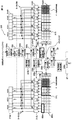
図3には、図2に示される構成による冗長救済の様子が示される。 FIG. 3 shows a state of redundancy relief by the configuration shown in FIG.
動作試験において、図3に示されるように、表示メモリ206の正規の記憶領域において、×印で示される箇所が不良と判断された場合、当該不良箇所を含むデータ線救済の対象箇所90、すなわち、転送用アドレスadd2に対応する領域が不良である旨が救済情報設定回路240bに設定される。この救済情報設定が行われた後は、データ線救済回路230bからのデータ線救済信号に基づいてセレクタ回路213の動作が制御されることにより、上記不良箇所を含むデータ線救済の対象箇所90(転送用アドレスadd2に対応する領域)からの出力データに代えて、データ線救済用領域(転送用アドレスadd7に対応する領域)からの出力データが選択的に論理回路214に伝達される。つまり、セレクタ回路213において、転送用アドレスadd0,add1、add3、add4、add5、add6に対応するラッチは、「−」で示される入力端子に伝達されたデータが選択的に論理回路214に伝達され、転送用アドレスadd2に対応するラッチ(80で示される)は、「+」で示される入力端子に伝達されたデータ、すなわち、転送用アドレスadd7に対応するデータ線救済用領域からのデータが選択的に論理回路214に伝達される。このようにデータ線救済回路230bからのデータ線救済信号に基づいてセレクタ回路213の動作が制御されることにより、上記不良箇所を含むデータ線救済の対象箇所90(転送用アドレスadd2に対応する領域)からの出力データに代えて、データ線救済用領域(転送用アドレスadd7に対応する領域)からの出力データが選択的に論理回路214に伝達されることによってデータ線救済が行われる。
In the operation test, as shown in FIG. 3, in the normal storage area of the
また、ワード線救済用領域を用いて救済したほうが良い場合には、救済情報設定回路240aに救済情報が設定され、ワード線救済回路230aにおいて、アドレス生成回路210の出力アドレスが救済設定回路240aに設定された救済情報と一致した場合には、正規の記憶領域におけるワード線に代えてワード線救済用領域のワード線が選択レベルに駆動されることによって、ワード線単位の救済が行われる。
If it is better to use the word line repair area, the repair information is set in the repair
上記例によれば、以下の作用効果を得ることができる。 According to the above example, the following operational effects can be obtained.
(1)メモリアレイから表示用データを読み出し、次段の回路に出力する場合、ワード線単位の救済は液晶表示装置100の表示位置に対応する必要がなく、選択するアドレスを変えるだけでよいが、データ線の救済は、表示装置の表示位置に対応するように、データの位置を入れ替える必要が生じる。図2に示される構成では、セレクタ回路213を設けることによって、上記データの位置の入れ替えが行われるため、データ線の救済を容易に行うことができる。
(1) When display data is read from the memory array and output to the next stage circuit, the relief for each word line does not need to correspond to the display position of the liquid
(2)汎用RAMで採用されている冗長回路は、正規のメモリ行もしくは列を選択する制御回路と、欠陥ビットと置き換えられる予備のメモリ行もしくは列(冗長メモリ)を選択する制御回路とが別個に設けられており、そのため、正規のメモリ行もしくは列をアクセスするときと、予備のメモリ行もしくは列をアクセスするときとで、読み出し速度などの動作特性が異なるため、メモリの周辺回路のタイミング設計が難しくなるのに対して、上記の例によれば、正規の行もしくは列を選択する制御回路と、欠陥ビットと置き換えられる予備の行もしくは列を選択する制御回路とを別個の回路として構成する必要がなく、それによって表示メモリ206の周辺回路のタイミング設計が容易となる。
(2) The redundancy circuit employed in the general-purpose RAM has a control circuit for selecting a normal memory row or column and a control circuit for selecting a spare memory row or column (redundant memory) to be replaced with a defective bit. As a result, the operating characteristics such as read speed differ between accessing a regular memory row or column and accessing a spare memory row or column. However, according to the above example, the control circuit for selecting a normal row or column and the control circuit for selecting a spare row or column to be replaced with a defective bit are configured as separate circuits. This is not necessary, and the timing design of the peripheral circuit of the
図4には、上記液晶コントローラドライバ200における主要部の別の構成例が示される。
FIG. 4 shows another configuration example of the main part of the liquid
図4に示される構成が、図2に示されるのと大きく相違するのは、表示メモリ206の出力データを、三状態(ハイ、ロー、高インピーダンス)回路の一例とされるクロックドインバータ回路312で受け、このクロックドインバータ回路312と論理回路214との間にアドレス共通のデータバスD−BUSを設けた点、及び転送用アドレス制御のための転送用アドレス制御回路250を設けた点である。
The configuration shown in FIG. 4 is greatly different from that shown in FIG. 2 in that the output data of the
上記クロックドインバータ回路312は、表示メモリ206の出力端子に対応して配置された複数のクロックドインバータを含む。この複数のクロックドインバータには、1画素に対応するデータサイズ毎に転送用アドレスadd0〜add7が割り当てられている。同様に論理回路214も複数の論理回路を含み、この複数の論理回路には1画素に対応するデータサイズ毎に転送用アドレスADD0〜ADD6が割り当てられている。上記クロックドインバータ回路312と論理回路214とはそれぞれ転送用アドレスによって時分割制御され、この時分割制御により、上記クロックドインバータ回路312の出力信号がデータバスD−BUSを介して論理回路214に伝達される。
The clocked
転送用アドレス制御回路250から論理回路214に対して転送用アドレス信号313が供給され、転送用アドレス制御回路250からクロックドインバータ回路312に対しては、データ線救済回路230bを介して転送用アドレス信号314が供給される。上記転送用アドレス信号313によって転送用アドレスADD0〜ADD6についての時分割制御が行われ、上記転送用アドレス信号314によって転送用アドレスadd0〜add7についての時分割制御が行われる。また、データ線救済回路230bでは、上記救済情報設定回路240bに設定された救済情報に従って、上記転送用アドレスの入れ替えを行う。例えば91で示される箇所がデータ線救済の対象とされるとき、図5に示されるように、データ線救済の対象箇所91に対応する転送用アドレスadd2が、データ線救済回路230bにおいて、データ線救済用領域に対応する転送用アドレスadd7に入れ替えられる。従って、上記時分割制御において、クロックドインバータ回路312から転送用アドレスadd0,add1,add7,add3,add4,add5,add6の順にデータバスD−BUSにデータ出力される。このとき、論理回路214では、転送用アドレスADD0,ADD1,ADD2,ADD3,ADD4,ADD5,ADD6の順にデータバスD−BUSからデータの取り込みが行われる。このように、クロックドインバータ312から論理回路214への時分割転送においては、データ線救済の対象箇所91からの出力データに代えて、データ線救済用領域からの出力データが論路回路214へ伝達されることによってデータ線救済が行われる。
A
上記の例によれば、以下の作用効果を得ることができる。 According to the above example, the following effects can be obtained.
(1)メモリアレイから表示用データを読み出し、次段の回路に出力する場合、ワード線単位の救済は表示装置の表示位置に対応する必要がなく、選択するアドレスを変えるだけでよいが、データ線の救済は、表示装置の表示位置に対応するように、データの位置を入れ替える必要が生じる。図4に示される構成では、表示メモリ206の出力データをクロックドインバータ回路312で受け、このクロックドインバータ回路312と論理回路214との間にアドレス共通のデータバスD−BUSを設け、さらに転送用アドレス制御のための転送用アドレス制御回路250を設けたことにより、表示メモリ206の欠陥を含む領域に対応する上記クロックドインバータに代えて、上記予備の記憶領域に対応する上記クロックドインバータをデータ出力状態に遷移させ、それによって、上記データの位置の入れ替えが行われるため、データ線の救済を容易に行うことができる。
(1) When display data is read from the memory array and output to the next stage circuit, the relief for each word line does not need to correspond to the display position of the display device, and only the address to be selected is changed. In line relief, it is necessary to change the position of the data so as to correspond to the display position of the display device. In the configuration shown in FIG. 4, the output data of the
(2)図4に示される構成によれば、図2に示されるセレクタ回路213が不要とされるため、チップ面積を縮小することができる。
(2) According to the configuration shown in FIG. 4, since the
図6には上記液晶コントローラドライバ200における主要部の別の構成例が示される。
FIG. 6 shows another configuration example of the main part of the liquid
図6に示される液晶コントローラドライバ200が図4に示されるのと大きく相違するのは、表示メモリ206がマット分割され、それに伴って周辺回路が配置されている点である。特に制限されないが、表示メモリ206は、左マット206Lと右マット206Rとに分割されている。上記左マット206Lに対応してクロックドインバータ回路312L、データバスD−BUSL、論理回路214L、アドレスデコーダ及びワード線ドライバ206CLが配置され、上記右マット206Lに対応してクロックドインバータ回路312R、データバスD−BUSR、論理回路214R、アドレスデコーダ及びワード線ドライバ206CRが配置される。上記左マット206L及び右マット206Rは、2のn乗のアドレス空間よりも小さな記憶領域とされる。ここで、上記「n」は、0を除く正の整数(1,2,3,…)とされる。このようにするのは、上記左マット206L及び右マット206Rにおけるデータ線救済用領域の転送用アドレスを確保し、それを予備の記憶領域に対応する上記クロックドインバータに割り当てるためである。すなわち、上記左マット206L及び右マット206Rを、2のn乗のアドレス空間よりも小さな記憶領域とした場合(本例では22よりも小さい3にしている)、図8に示されるように、3ビットアドレスA2,A1,A0のうち下位アドレスA1,A0のみに着目した場合の擬似的な未活用アドレス「11」,「10」を確保している。データ線救済回路230bでは、上記未活用アドレス「11」によって上記左マット206Lにおけるデータ線救済用領域が選択され、上記未活用アドレス「10」によって上記右マット206Rにおけるデータ線救済用領域が選択される。
The liquid
例えば図6において、91L,91Rで示される箇所がデータ線救済の対象とされる場合、以下のように救済される。すなわち、データ線救済回路230bは、救済情報設定回路240bの記憶情報に基づいて、アドレス「010」に代えてマット206L側の「11」を選択する。これにより時分割転送においては、図7に示されるように、左マット206L側の転送用アドレスadd2に代えて、add3に対応するクロックドインバータが活性化される。また、右マット206R側の転送用アドレスadd1に代えて、add3に対応するクロックドインバータが活性化される。
For example, in FIG. 6, when the locations indicated by 91L and 91R are the target of data line repair, the repair is performed as follows. That is, the data
上記例によれば、以下の作用効果を得ることができる。 According to the above example, the following operational effects can be obtained.
表示メモリ206がマット分割されている場合でも、左マット206L、右マット206Rの出力データをクロックドインバータ回路312L,312Rで受け、このクロックドインバータ回路312L,312Rと論理回路214L,214Rとの間にデータバスD−BUSL,D−BUSRを設け、さらに転送用アドレス制御のための転送用アドレス制御回路250を設けたことにより、左マット206L、右マット206Rにおいて欠陥を含む領域に対応する上記クロックドインバータに代えて、上記予備の記憶領域に対応する上記クロックドインバータをデータ出力状態に遷移させ、それによって、上記データの位置の入れ替えが行われるため、図4に示される場合と同様に、データ線の救済を容易に行うことができる。
Even when the
図9には上記液晶コントローラドライバ200における主要部の別の構成例が示される。
FIG. 9 shows another configuration example of the main part of the liquid
図9に示される液晶コントローラドライバ200が図6に示されるのと大きく相違するのは、データバスD−BUSが左マット206L、右マット206Rに対応して分割されていない点である。
The liquid
データ線救済回路230bからクロックドインバータ回路312L,312Rに供給される転送アドレス信号は、図11に示されるように3ビット構成(A2,A2,A1)とされる。このうち、A0ビットが「0」の場合にクロックドインバータ回路312Lが選択され、A0ビットが「1」の場合にクロックドインバータ回路312Rが選択される。A1,A2は着目ビットとされ、このA1,A2により、クロックドインバータ回路312L又は312Rにおける個々のクロックドインバータが活性化される。
The transfer address signal supplied from the data
図10には、論理回路214L,214Rの転送アドレスとクロックドインバータ回路312L,312Rの転送アドレスとの関係が示される。
FIG. 10 shows the relationship between the transfer addresses of the
91L,91Rで示される箇所がデータ線救済の対象とされる。このときデータ線救済回路230bの制御により、データ線救済91Lに対応するクロックドインバータの転送用アドレスadd4に代えて転送用アドレスadd6が選択されることによって、左マット206Lにおけるデータ線救済用領域が使用される。データ線救済91Rに対応するクロックドインバータの転送用アドレスadd3に代えて転送用アドレスadd7が選択されることによって、左マット206Lにおけるデータ線救済用領域が使用される。
The locations indicated by 91L and 91R are targeted for data line relief. At this time, under the control of the data
上記例によれば、以下の作用効果を得ることができる。 According to the above example, the following operational effects can be obtained.
(1)表示メモリ206がマット分割されている場合でも、左マット206L、右マット206Rの出力データをクロックドインバータ回路312L,312Rで受け、このクロックドインバータ回路312L,312Rと論理回路214L,214Rとの間にデータバスD−BUSを設け、さらに転送用アドレス制御のための転送用アドレス制御回路250を設けたことにより、左マット206L、右マット206Rにおいて欠陥を含む領域に対応する上記クロックドインバータに代えて、上記予備の記憶領域に対応する上記クロックドインバータをデータ出力状態に遷移させ、それによって、上記データの位置の入れ替えが行われるため、図4に示される場合と同様に、データ線の救済を容易に行うことができる。
(1) Even when the
(2)データバスD−BUSが左マット206L、右マット206Rに対応して分割されていないので、論理回路214L,214Rにおける転送用アドレスADD0〜ADD5に対するデータの並びを任意に変更することができる。
(2) Since the data bus D-BUS is not divided corresponding to the
図12には上記液晶コントローラドライバ200における主要部の別の構成例が示される。
FIG. 12 shows another configuration example of the main part of the liquid
図12に示される液晶コントローラドライバ200が図4に示されるのと大きく相違するのは、論理回路214側に論理回路側データバスD−BUS−1が配置され、クロックドインバータ回路312側にクロックドインバータ回路側データバスD−BUS−2が配置され、上記論理回路側データバスD−BUS−1とクロックドインバータ回路側データバスD−BUS−2との間に論理回路97が配置された点である。上記論理回路97での処理には、表示カラーを変換するするためのカラー変換処理や、文字の大きさを変更するための倍角処理などが含まれる。
The
上記例によれば、以下の作用効果を得ることができる。 According to the above example, the following operational effects can be obtained.
(1)上記論理回路側データバスD−BUS−1とクロックドインバータ回路側データバスD−BUS−2との間に論理回路97が配置された場合には、図6に示されるのと同様に、表示メモリ206の欠陥を含む領域に対応する上記クロックドインバータに代えて、上記予備の記憶領域に対応する上記クロックドインバータをデータ出力状態に遷移させ、それによって、上記データの位置の入れ替えが行われるため、データ線の救済を容易に行うことができる。
(1) When the
(2)上記論理回路側データバスD−BUS−1とクロックドインバータ回路側データバスD−BUS−2との間に論理回路97が配置されているので、表示データに対してカラー変換処理や倍角処理などの画像処理を一括して行うことができる。
(2) Since the
図13には上記液晶コントローラドライバ200における主要部の別の構成例が示される。
FIG. 13 shows another configuration example of the main part of the liquid
図13に示される液晶コントローラドライバ200が図4に示されるのと大きく相違するのは、内外部アドレスを内部アドレスに変換するようにした点である。インタフェース87を介してワード線アドレス信号やデータ線アドレス信号が取り込まれる。上記ワード線アドレス信号はワード線アドレス制御回路88に伝達される。救済情報設定回路240cにはワード線救済情報が設定されており、ワード線救済回路230aは、救済情報設定回路240cに設定されたワード線救済情報に従ってワード線救済を行う。インタフェース87を介して外部から取り込まれたデータ線アドレス信号A2,A1,A0はデータ線アドレス制御回路89を介して内部アドレス変換回路86に伝達される。この内部アドレス変換回路86は、入力されたデータ線アドレス信号A2,A1,A0を、内部アドレス信号a1,a0と、マット選択信号m0とに変換する。内部アドレス信号a1,a0と、マット選択信号m0は、後段に配置されたデータ線救済回路230cに伝達される。このデータ線救済回路230cは、上記内部アドレス変換回路86から伝達されたデータ線アドレス信号と、救済情報設定回路に設定されている救済情報とを比較し、それらが一致していた場合には、データ線救済のために表示メモリ206へのデータ書込みアドレスの入れ替えを行う。上記マット選択信号m0は、書込み用タイミング制御回路203bに伝達される。この書込み用タイミング制御回路203bは、マット選択信号m0に基づいて、上記表示メモリ206へのデータ書込みの際のマット選択を行う。書込みのためのデータは、ライトデータラッチ208を介し取り込まれる。
The liquid
転送用タイミング制御回路203aが設けられ、この転送用タイミング制御回路203aは、図示されないインタフェースなどを介して伝達された制御信号に基づいて転送タイミングを制御する。転送用アドレス制御回路250が設けられ、この転送用アドレス制御回路250は、上記転送用タイミング制御回路203aからのタイミング制御信号に同期して、論理回路214L,214Rにおける各論理回路を選択的に書込み状態にするための転送用アドレス信号を発生する。データ線救済回路230bは、上記転送用アドレス制御回路250から伝達された転送用アドレス信号と上記救済情報設定回路240bに設定されている救済情報とを比較し、それらが一致していた場合には、データ線救済のためにクロックドインバータ回路312L,312Rにおける個々のクロックドインバータの活性化するための転送用アドレス信号の入れ替えを行う。尚、91L,91Rで示される箇所がデータ線救済の対象とされる場合において、時分割転送によりデータの入れ替えが行われるのは、例えば図6に示される構成の場合と同様であるので、それについての詳細な説明は省略する。
A transfer
図14には、外部アドレス(データ線アドレスA2,A1,A0)と内部アドレスとの対応関係が示される。内部アドレス変換を行わないで、外部から見たアドレスだけで制御する場合には、マット毎にadd0〜add2に対応するA2,A1,A0は各マット毎に異なってしまう。それに対して図13に示される構成において内部アドレス変換を行う場合には、マット内の内部アドレス(a1,a0)は繰り返しとなる。また、外部アドレスによれば、ADD2とADD3(左マットにおけるadd2と右マットにおけるadd0)は連続しており、液晶コントローラドライバ200の製造において表示メモリ206の取り扱いが容易となる。
FIG. 14 shows the correspondence between external addresses (data line addresses A2, A1, A0) and internal addresses. When the internal address conversion is not performed and the control is performed using only the addresses viewed from the outside, A2, A1, and A0 corresponding to add0 to add2 are different for each mat. On the other hand, when internal address conversion is performed in the configuration shown in FIG. 13, the internal addresses (a1, a0) in the mat are repeated. Further, according to the external address, ADD2 and ADD3 (add2 in the left mat and add0 in the right mat) are continuous, and the
上記例によれば、以下の作用効果を得ることができる。 According to the above example, the following operational effects can be obtained.
(1)左マット206L、右マット206Rにおいて欠陥を含む領域に対応する上記クロックドインバータに代えて、上記予備の記憶領域に対応する上記クロックドインバータをデータ出力状態に遷移させ、それによって、上記データの位置の入れ替えが行われるため、図4、図6、図9に示される場合と同様に、データ線の救済を容易に行うことができる。
(1) Instead of the clocked inverter corresponding to the area including the defect in the
(2)内部アドレス変換を行うことによって、マット内の内部アドレス(a1,a0)は繰り返しとなるこのため、多マット構成の場合ほど、制御、レイアウト設計、検証が容易になるという利点がある。また、データ線救済用領域(冗長領域)に対応するアドレスは、どのマットでも同じになるため、救済情報の取り扱いも容易となる。例えば救済が必要無い場合は救済情報は「11」とし、マットの左端のデータ線救済を行う場合の救済情報は「00」とすれば良く、救済情報の単純化を図ることができる。 (2) By performing the internal address conversion, the internal addresses (a1, a0) in the mat are repeated. Therefore, there is an advantage that control, layout design, and verification become easier as in the case of a multi-mat configuration. In addition, since the addresses corresponding to the data line relief area (redundant area) are the same in any mat, the relief information can be easily handled. For example, if no relief is required, the relief information may be “11”, and the relief information when performing data line relief on the left end of the mat may be “00”, so that the relief information can be simplified.
図15には上記液晶コントローラドライバ200における主要部の別の構成例が示される。
FIG. 15 shows another configuration example of a main part in the liquid
図15に示される液晶コントローラドライバ200が図4に示されるのと大きく相違するのは、クロックドインバータ回路312とデータバスD−BUSとの間に、アドレスシフトのためのアドレスシフタ85を設けた点である。すなわち、91で示される箇所がデータ線救済の対象とされるとき、このアドレスシフタ85は、特に制限されないが、救済情報設定回路240bに設定された救済情報に従って、上記データ線救済対象に対応するクロックドインバータが非選択状態とされ、当該クロックドインバータの右側に存在するクロックドインバータが選択される。このとき、上記データ線救済対象に対応するクロックドインバータが非選択状態とされているため、1画素分づつシフトされてデータ線救済用領域に対応するクロックドインバータが選択されることでデータ線の救済が行われる。そして、図16に示されるように、データバスD−BUSを介してデータの時分割転送が行われる。
The liquid
図17には上記液晶コントローラドライバ200における主要部の別の構成例が示される。
FIG. 17 shows another configuration example of the main part of the liquid
図17に示される液晶コントローラドライバ200が図2に示されるのと大きく相違するのは、救済情報設定回路240bに設定された救済情報に基づいてセレクタ213により選択データがシフトされる点にある。セレクタ回路213における個々のセレクタは、それに対応するクロックドインバータの出力データと、それに隣接するクロックドインバータの出力データとを選択的に論理回路215に伝達する。91で示される箇所がデータ線救済の対象とされてデータ線救済が行われている場合には、セレクタ213により、91で示される箇所に対応するクロックドインバータ(転送アドレスadd1に対応するもの)の出力は非選択状態とされ、選択データが1画素分づつシフトされることによってデータ線救済が行われる。かかる構成においては、救済されるデータ線にかかわらず、クロックドインバータ212から論理回路215までのデータ伝達経路の長さがほぼ等しくなるので、上記データ伝達経路での遅延時間のばらつきを考慮する必要が無い。
The liquid
以上本発明者によってなされた発明を具体的に説明したが、本発明はそれに限定されるものではなく、その要旨を逸脱しない範囲で種々変更可能であることはいうまでもない。 Although the invention made by the present inventor has been specifically described above, the present invention is not limited thereto, and it goes without saying that various changes can be made without departing from the scope of the invention.
以上の説明では主として本発明者によってなされた発明をその背景となった利用分野である液晶パネル用の駆動信号を生成して出力する液晶コントローラドライバに適用した場合を説明したが、本発明はこれに限定されるものでなく、有機EL表示パネルなど液晶以外の表示装置を駆動する表示制御用半導体集積回路にも利用することができる。 In the above description, the case where the invention made mainly by the present inventor is applied to a liquid crystal controller driver that generates and outputs a drive signal for a liquid crystal panel, which is the field of use behind the invention, has been described. The present invention is not limited to this, and it can also be used for a display control semiconductor integrated circuit for driving a display device other than a liquid crystal such as an organic EL display panel.
200 液晶コントローラドライバ
206 表示メモリ
210 アドレス生成回路
212 212ラッチ回路
213 セレクタ回路
214 論理回路
215 ソース線駆動回路
230 救済回路
240 救済情報設定回路
312 クロックドインバータ
D−BUS データバス
200 Liquid
Claims (8)
上記表示データを記憶する正規の記憶領域以外に設けられた予備の記憶領域と、
上記表示メモリの欠陥を含む領域を上記予備の記憶領域に置き換えることで欠陥救済を可能とする救済回路と、
上記表示メモリからの出力データの伝達経路に設けられ、上記正規の記憶領域からの出力データを、上記救済回路からの制御信号に応じて選択的に上記予備の記憶領域からの出力データに置き換えるためのセレクタ回路と、を含むことを特徴とする表示制御用半導体集積回路。 A display memory having a storage area and capable of storing display data on the display device in the storage area;
A spare storage area provided in addition to the regular storage area for storing the display data;
A repair circuit capable of repairing a defect by replacing an area including a defect of the display memory with the spare storage area;
Provided in the transmission path of the output data from the display memory, in order to selectively replace the output data from the regular storage area with the output data from the spare storage area in accordance with a control signal from the relief circuit A display control semiconductor integrated circuit comprising: a selector circuit;
上記表示データを記憶する正規の記憶領域以外に設けられた予備の記憶領域と、
上記表示メモリの欠陥を含む領域を上記予備の記憶領域に置き換えることで欠陥救済を可能とする救済回路と、
上記表示メモリからの出力データを後段回路に伝達するためのデータバスと、
上記表示メモリのデータ出力端子に対応して設けられ、それぞれ上記表示メモリのデータ出力端子からの出力データを上記データバスに供給可能な複数の三状態回路と、
上記データバスを介して上記表示メモリから伝達されたデータを取り込むための論理回路と、
上記複数の三状態回路を時分割により順次データ出力状態に遷移させるための制御回路と、を含み、
上記救済回路は、上記表示メモリの欠陥を含む領域に対応する上記三状態回路に代えて、上記予備の記憶領域に対応する上記三状態回路をデータ出力状態に遷移させることを特徴とする表示制御用半導体集積回路。 A display memory having a storage area and capable of storing display data on the display device in the storage area;
A spare storage area provided in addition to the regular storage area for storing the display data;
A repair circuit capable of repairing a defect by replacing an area including a defect of the display memory with the spare storage area;
A data bus for transmitting output data from the display memory to a subsequent circuit;
A plurality of three-state circuits provided corresponding to the data output terminals of the display memory, each capable of supplying output data from the data output terminals of the display memory to the data bus;
A logic circuit for fetching data transmitted from the display memory via the data bus;
A control circuit for sequentially shifting the plurality of three-state circuits to a data output state by time division,
The relief circuit shifts the three-state circuit corresponding to the spare storage area to a data output state instead of the three-state circuit corresponding to the area including the defect of the display memory. Semiconductor integrated circuit.
上記第1データバスと上記第2データバスとは、入力データに対する所定の論理演算を可能とする論理回路を介してデータのやり取りが可能とされる請求項4記載の表示制御用半導体集積回路。 The data bus includes a first data bus to which an output terminal of the tristate circuit is coupled, and a second data bus to which an input terminal of the logic circuit is coupled,
5. The display control semiconductor integrated circuit according to claim 4, wherein the first data bus and the second data bus can exchange data via a logic circuit capable of performing a predetermined logic operation on input data.
上記表示データを記憶する正規の記憶領域以外に設けられた予備の記憶領域と、
上記表示メモリの欠陥を含む領域を上記予備の記憶領域に置き換えることで欠陥救済を可能とする救済回路と、
上記表示メモリの出力データを後段回路に伝達するためのデータバスと、
上記表示メモリのデータ出力端子に対応して設けられ、それぞれ上記表示メモリのデータ出力端子からの出力データを上記データバスに供給可能な複数の三状態回路と、
上記データバスを介して上記表示メモリから伝達されたデータを取り込むための論理回路と、
上記複数の三状態回路と上記論理回路との間のデータ伝達経路に配置され、救済情報に応じて上記三状態回路を選択するためのアドレスをシフトすることによって、上記表示メモリの欠陥を含む領域に対応する上記三状態回路に代えて、上記予備の記憶領域に対応する上記三状態回路をデータ出力状態に遷移させるためのアドレスシフタと、を含むことを特徴とする表示制御用半導体集積回路。 A display memory having a storage area and capable of storing display data on the display device in the storage area;
A spare storage area provided in addition to the regular storage area for storing the display data;
A repair circuit capable of repairing a defect by replacing an area including a defect of the display memory with the spare storage area;
A data bus for transmitting the output data of the display memory to a subsequent circuit;
A plurality of three-state circuits provided corresponding to the data output terminals of the display memory, each capable of supplying output data from the data output terminals of the display memory to the data bus;
A logic circuit for fetching data transmitted from the display memory via the data bus;
An area including a defect in the display memory, arranged in a data transmission path between the plurality of three-state circuits and the logic circuit, by shifting an address for selecting the three-state circuit according to relief information An address shifter for transitioning the three-state circuit corresponding to the spare storage area to a data output state, instead of the three-state circuit corresponding to the display, and a display control semiconductor integrated circuit.
Priority Applications (5)
| Application Number | Priority Date | Filing Date | Title |
|---|---|---|---|
| JP2006293766A JP2008111921A (en) | 2006-10-30 | 2006-10-30 | Semiconductor integrated circuit for display control |
| US11/869,976 US7979755B2 (en) | 2006-10-30 | 2007-10-10 | Semiconductor integrated circuit device for display controller |
| TW096139857A TWI442375B (en) | 2006-10-30 | 2007-10-24 | And a semiconductor integrated circuit for display control |
| KR1020070108884A KR20080039272A (en) | 2006-10-30 | 2007-10-29 | Semiconductor Integrated Circuits for Display Control |
| CN2007101675771A CN101174404B (en) | 2006-10-30 | 2007-10-29 | Semiconductor integrated circuit device for display controller |
Applications Claiming Priority (1)
| Application Number | Priority Date | Filing Date | Title |
|---|---|---|---|
| JP2006293766A JP2008111921A (en) | 2006-10-30 | 2006-10-30 | Semiconductor integrated circuit for display control |
Publications (1)
| Publication Number | Publication Date |
|---|---|
| JP2008111921A true JP2008111921A (en) | 2008-05-15 |
Family
ID=39331839
Family Applications (1)
| Application Number | Title | Priority Date | Filing Date |
|---|---|---|---|
| JP2006293766A Pending JP2008111921A (en) | 2006-10-30 | 2006-10-30 | Semiconductor integrated circuit for display control |
Country Status (5)
| Country | Link |
|---|---|
| US (1) | US7979755B2 (en) |
| JP (1) | JP2008111921A (en) |
| KR (1) | KR20080039272A (en) |
| CN (1) | CN101174404B (en) |
| TW (1) | TWI442375B (en) |
Families Citing this family (4)
| Publication number | Priority date | Publication date | Assignee | Title |
|---|---|---|---|---|
| TW201237831A (en) * | 2011-03-11 | 2012-09-16 | Raydium Semiconductor Corp | Liquid crystal display driver and display device having the same |
| KR102305502B1 (en) * | 2014-12-22 | 2021-09-28 | 삼성디스플레이 주식회사 | Scanline driver chip and display device including the same |
| KR20190064098A (en) * | 2017-11-30 | 2019-06-10 | 에스케이하이닉스 주식회사 | Semiconductor device, and repair operation method thereof |
| US10978028B2 (en) * | 2018-09-17 | 2021-04-13 | Apple Inc. | Correction for defective memory of a memory-in-pixel display |
Citations (4)
| Publication number | Priority date | Publication date | Assignee | Title |
|---|---|---|---|---|
| JPS62275291A (en) * | 1980-04-11 | 1987-11-30 | アムペツクス コーポレーション | Computer graphic system |
| JP2001085644A (en) * | 2000-07-12 | 2001-03-30 | Hitachi Ltd | Method for manufacturing semiconductor device |
| JP2001189094A (en) * | 1999-12-28 | 2001-07-10 | Toshiba Corp | Memory space control device, semiconductor integrated circuit device, and integrated circuit system |
| JP2004233742A (en) * | 2003-01-31 | 2004-08-19 | Renesas Technology Corp | Electronic device having display drive control device and display device |
Family Cites Families (20)
| Publication number | Priority date | Publication date | Assignee | Title |
|---|---|---|---|---|
| JP3083547B2 (en) * | 1990-07-12 | 2000-09-04 | 株式会社日立製作所 | Semiconductor integrated circuit device |
| US5383162A (en) * | 1991-08-26 | 1995-01-17 | Hitachi, Ltd. | Semiconductor memory device |
| JPH06275095A (en) * | 1993-03-18 | 1994-09-30 | Fujitsu Ltd | Semiconductor memory and writing method for redundant address |
| KR970707555A (en) * | 1994-11-15 | 1997-12-01 | 로버트 에프. 도너후 | Circuits, systems, and methods for replacing defective cells in memory devices (CIRCUITS, SYSTEMS, AND METHODS FOR ACCOUNTING FOR DEFECTIVE CELLS IN A MEMORY DEVICE) |
| JP3631277B2 (en) * | 1995-01-27 | 2005-03-23 | 株式会社日立製作所 | Memory module |
| JP2710235B2 (en) * | 1995-08-30 | 1998-02-10 | 日本電気株式会社 | Defect relief judgment circuit |
| JP3476646B2 (en) * | 1997-03-07 | 2003-12-10 | シャープ株式会社 | Semiconductor storage device |
| US6085288A (en) * | 1997-04-14 | 2000-07-04 | International Business Machines Corporation | Dual cache directories with respective queue independently executing its content and allowing staggered write operations |
| JPH117761A (en) * | 1997-06-13 | 1999-01-12 | Toshiba Corp | Image memory |
| CN1181383C (en) * | 1999-03-08 | 2004-12-22 | 松下电器产业株式会社 | Liquid crystal display device and inspection method thereof |
| US6157584A (en) * | 1999-05-20 | 2000-12-05 | Advanced Micro Devices, Inc. | Redundancy circuit and method for semiconductor memory |
| JP2000347646A (en) | 1999-06-07 | 2000-12-15 | Hitachi Ltd | Display control device and display system |
| JP3863330B2 (en) * | 1999-09-28 | 2006-12-27 | 株式会社東芝 | Nonvolatile semiconductor memory |
| US6567323B2 (en) * | 2001-02-27 | 2003-05-20 | Texas Instruments Incorporated | Memory circuit redundancy control |
| US6966012B1 (en) * | 2001-06-22 | 2005-11-15 | Artisan Components, Inc. | Memory column redundancy circuitry and method for implementing the same |
| JP2003068093A (en) * | 2001-08-28 | 2003-03-07 | Mitsubishi Electric Corp | Semiconductor storage device |
| JP4270832B2 (en) * | 2002-09-26 | 2009-06-03 | 株式会社東芝 | Nonvolatile semiconductor memory |
| JP4427361B2 (en) * | 2004-03-16 | 2010-03-03 | 株式会社東芝 | Nonvolatile semiconductor memory |
| US6991947B1 (en) * | 2004-03-22 | 2006-01-31 | Tushar Gheewala | Hybrid semiconductor circuit with programmable intraconnectivity |
| CN100365494C (en) * | 2004-12-20 | 2008-01-30 | 凌阳科技股份有限公司 | Thin film transistor liquid crystal display with function of repairing broken line and high-impedance detection circuit |
-
2006
- 2006-10-30 JP JP2006293766A patent/JP2008111921A/en active Pending
-
2007
- 2007-10-10 US US11/869,976 patent/US7979755B2/en not_active Expired - Fee Related
- 2007-10-24 TW TW096139857A patent/TWI442375B/en not_active IP Right Cessation
- 2007-10-29 CN CN2007101675771A patent/CN101174404B/en not_active Expired - Fee Related
- 2007-10-29 KR KR1020070108884A patent/KR20080039272A/en not_active Withdrawn
Patent Citations (4)
| Publication number | Priority date | Publication date | Assignee | Title |
|---|---|---|---|---|
| JPS62275291A (en) * | 1980-04-11 | 1987-11-30 | アムペツクス コーポレーション | Computer graphic system |
| JP2001189094A (en) * | 1999-12-28 | 2001-07-10 | Toshiba Corp | Memory space control device, semiconductor integrated circuit device, and integrated circuit system |
| JP2001085644A (en) * | 2000-07-12 | 2001-03-30 | Hitachi Ltd | Method for manufacturing semiconductor device |
| JP2004233742A (en) * | 2003-01-31 | 2004-08-19 | Renesas Technology Corp | Electronic device having display drive control device and display device |
Also Published As
| Publication number | Publication date |
|---|---|
| CN101174404B (en) | 2011-10-05 |
| US20080104457A1 (en) | 2008-05-01 |
| TW200837712A (en) | 2008-09-16 |
| CN101174404A (en) | 2008-05-07 |
| KR20080039272A (en) | 2008-05-07 |
| TWI442375B (en) | 2014-06-21 |
| US7979755B2 (en) | 2011-07-12 |
Similar Documents
| Publication | Publication Date | Title |
|---|---|---|
| US8068113B2 (en) | Display control semiconductor integrated circuit | |
| US7471573B2 (en) | Integrated circuit device and electronic instrument | |
| TWI431601B (en) | And a semiconductor integrated circuit for display control | |
| JP2009016037A (en) | Flash memory having high redundancy efficiency, integrated circuit memory device, and driving method of flash memory device | |
| JPH04303233A (en) | Integrated circuit for display driving control and display system | |
| US7590015B2 (en) | Integrated circuit device and electronic instrument | |
| CN101174404B (en) | Semiconductor integrated circuit device for display controller | |
| US7605434B2 (en) | Semiconductor memory device to which test data is written | |
| US9940906B2 (en) | Storage device, display driver, electro-optical device, and electronic apparatus | |
| US7698607B2 (en) | Repairing microdisplay frame buffers | |
| JP2009128603A (en) | Display drive circuit | |
| KR100809715B1 (en) | Fixed control data generation circuit and display driver circuit having same | |
| US10643515B2 (en) | Display driver, display device and method of operating display driver | |
| JP2005174533A (en) | Semiconductor device, electronic device, ic card, and method for driving semiconductor device | |
| KR100600956B1 (en) | SRAM with fast write time and driving method therefor | |
| KR0150857B1 (en) | Semiconductor memory device | |
| JP2009217021A (en) | Image display device | |
| JP2007188335A (en) | Image data processor and frame memory |
Legal Events
| Date | Code | Title | Description |
|---|---|---|---|
| A621 | Written request for application examination |
Free format text: JAPANESE INTERMEDIATE CODE: A621 Effective date: 20091021 |
|
| A711 | Notification of change in applicant |
Free format text: JAPANESE INTERMEDIATE CODE: A712 Effective date: 20100507 |
|
| A131 | Notification of reasons for refusal |
Free format text: JAPANESE INTERMEDIATE CODE: A131 Effective date: 20120510 |
|
| A02 | Decision of refusal |
Free format text: JAPANESE INTERMEDIATE CODE: A02 Effective date: 20120906 |