JP2007217227A - GaN crystal manufacturing method, GaN crystal substrate, and semiconductor device - Google Patents
GaN crystal manufacturing method, GaN crystal substrate, and semiconductor device Download PDFInfo
- Publication number
- JP2007217227A JP2007217227A JP2006039411A JP2006039411A JP2007217227A JP 2007217227 A JP2007217227 A JP 2007217227A JP 2006039411 A JP2006039411 A JP 2006039411A JP 2006039411 A JP2006039411 A JP 2006039411A JP 2007217227 A JP2007217227 A JP 2007217227A
- Authority
- JP
- Japan
- Prior art keywords
- gan crystal
- gan
- crystal substrate
- seed crystal
- substrate
- Prior art date
- Legal status (The legal status is an assumption and is not a legal conclusion. Google has not performed a legal analysis and makes no representation as to the accuracy of the status listed.)
- Pending
Links
- 239000013078 crystal Substances 0.000 title claims abstract description 265
- 239000000758 substrate Substances 0.000 title claims abstract description 121
- 238000004519 manufacturing process Methods 0.000 title claims abstract description 43
- 239000004065 semiconductor Substances 0.000 title claims abstract description 22
- 238000000034 method Methods 0.000 claims abstract description 39
- 238000002248 hydride vapour-phase epitaxy Methods 0.000 claims abstract description 26
- 238000005092 sublimation method Methods 0.000 claims abstract description 13
- 239000012535 impurity Substances 0.000 claims description 23
- 238000002441 X-ray diffraction Methods 0.000 claims description 10
- 239000010703 silicon Substances 0.000 claims description 6
- 229910052710 silicon Inorganic materials 0.000 claims description 6
- QVGXLLKOCUKJST-UHFFFAOYSA-N atomic oxygen Chemical compound [O] QVGXLLKOCUKJST-UHFFFAOYSA-N 0.000 claims description 4
- 239000001301 oxygen Substances 0.000 claims description 4
- 229910052760 oxygen Inorganic materials 0.000 claims description 4
- 239000007789 gas Substances 0.000 description 103
- IJGRMHOSHXDMSA-UHFFFAOYSA-N Atomic nitrogen Chemical compound N#N IJGRMHOSHXDMSA-UHFFFAOYSA-N 0.000 description 40
- GYHNNYVSQQEPJS-UHFFFAOYSA-N Gallium Chemical compound [Ga] GYHNNYVSQQEPJS-UHFFFAOYSA-N 0.000 description 39
- 229910052733 gallium Inorganic materials 0.000 description 39
- 229910052757 nitrogen Inorganic materials 0.000 description 18
- 229910052736 halogen Inorganic materials 0.000 description 13
- 150000002367 halogens Chemical class 0.000 description 13
- 238000010438 heat treatment Methods 0.000 description 12
- 239000002994 raw material Substances 0.000 description 12
- 239000012159 carrier gas Substances 0.000 description 9
- XOYLJNJLGBYDTH-UHFFFAOYSA-M chlorogallium Chemical compound [Ga]Cl XOYLJNJLGBYDTH-UHFFFAOYSA-M 0.000 description 7
- VEXZGXHMUGYJMC-UHFFFAOYSA-N Hydrochloric acid Chemical compound Cl VEXZGXHMUGYJMC-UHFFFAOYSA-N 0.000 description 6
- 229910000041 hydrogen chloride Inorganic materials 0.000 description 6
- IXCSERBJSXMMFS-UHFFFAOYSA-N hydrogen chloride Substances Cl.Cl IXCSERBJSXMMFS-UHFFFAOYSA-N 0.000 description 6
- XUIMIQQOPSSXEZ-UHFFFAOYSA-N Silicon Chemical compound [Si] XUIMIQQOPSSXEZ-UHFFFAOYSA-N 0.000 description 5
- 238000005530 etching Methods 0.000 description 5
- 239000000463 material Substances 0.000 description 5
- 229910001873 dinitrogen Inorganic materials 0.000 description 4
- 229910052751 metal Inorganic materials 0.000 description 4
- 239000002184 metal Substances 0.000 description 4
- NJPPVKZQTLUDBO-UHFFFAOYSA-N novaluron Chemical compound C1=C(Cl)C(OC(F)(F)C(OC(F)(F)F)F)=CC=C1NC(=O)NC(=O)C1=C(F)C=CC=C1F NJPPVKZQTLUDBO-UHFFFAOYSA-N 0.000 description 4
- 238000000859 sublimation Methods 0.000 description 4
- 230000008022 sublimation Effects 0.000 description 4
- UFHFLCQGNIYNRP-UHFFFAOYSA-N Hydrogen Chemical compound [H][H] UFHFLCQGNIYNRP-UHFFFAOYSA-N 0.000 description 3
- 238000011109 contamination Methods 0.000 description 3
- 239000000843 powder Substances 0.000 description 3
- 230000005855 radiation Effects 0.000 description 3
- 229910052594 sapphire Inorganic materials 0.000 description 3
- 239000010980 sapphire Substances 0.000 description 3
- 238000001004 secondary ion mass spectrometry Methods 0.000 description 3
- 230000003746 surface roughness Effects 0.000 description 3
- QGZKDVFQNNGYKY-UHFFFAOYSA-N Ammonia Chemical compound N QGZKDVFQNNGYKY-UHFFFAOYSA-N 0.000 description 2
- XKRFYHLGVUSROY-UHFFFAOYSA-N Argon Chemical compound [Ar] XKRFYHLGVUSROY-UHFFFAOYSA-N 0.000 description 2
- 229910001218 Gallium arsenide Inorganic materials 0.000 description 2
- 229910021098 KOH—NaOH Inorganic materials 0.000 description 2
- 208000012868 Overgrowth Diseases 0.000 description 2
- 229910004298 SiO 2 Inorganic materials 0.000 description 2
- 238000005520 cutting process Methods 0.000 description 2
- UPWPDUACHOATKO-UHFFFAOYSA-K gallium trichloride Chemical compound Cl[Ga](Cl)Cl UPWPDUACHOATKO-UHFFFAOYSA-K 0.000 description 2
- 238000001451 molecular beam epitaxy Methods 0.000 description 2
- 238000005498 polishing Methods 0.000 description 2
- 238000002360 preparation method Methods 0.000 description 2
- 239000010453 quartz Substances 0.000 description 2
- VYPSYNLAJGMNEJ-UHFFFAOYSA-N silicon dioxide Inorganic materials O=[Si]=O VYPSYNLAJGMNEJ-UHFFFAOYSA-N 0.000 description 2
- 238000004544 sputter deposition Methods 0.000 description 2
- WFKWXMTUELFFGS-UHFFFAOYSA-N tungsten Chemical compound [W] WFKWXMTUELFFGS-UHFFFAOYSA-N 0.000 description 2
- 229910052721 tungsten Inorganic materials 0.000 description 2
- 239000010937 tungsten Substances 0.000 description 2
- JMASRVWKEDWRBT-UHFFFAOYSA-N Gallium nitride Chemical compound [Ga]#N JMASRVWKEDWRBT-UHFFFAOYSA-N 0.000 description 1
- 230000002378 acidificating effect Effects 0.000 description 1
- 238000004458 analytical method Methods 0.000 description 1
- 229910052786 argon Inorganic materials 0.000 description 1
- 230000015572 biosynthetic process Effects 0.000 description 1
- 238000005229 chemical vapour deposition Methods 0.000 description 1
- 230000000052 comparative effect Effects 0.000 description 1
- MROCJMGDEKINLD-UHFFFAOYSA-N dichlorosilane Chemical compound Cl[SiH2]Cl MROCJMGDEKINLD-UHFFFAOYSA-N 0.000 description 1
- 230000005669 field effect Effects 0.000 description 1
- 239000011261 inert gas Substances 0.000 description 1
- 238000010030 laminating Methods 0.000 description 1
- 238000001459 lithography Methods 0.000 description 1
- 238000012986 modification Methods 0.000 description 1
- 230000004048 modification Effects 0.000 description 1
- 150000004767 nitrides Chemical class 0.000 description 1
- 230000003287 optical effect Effects 0.000 description 1
- 238000000059 patterning Methods 0.000 description 1
- 230000002093 peripheral effect Effects 0.000 description 1
- 238000007517 polishing process Methods 0.000 description 1
- 230000009257 reactivity Effects 0.000 description 1
- 230000001105 regulatory effect Effects 0.000 description 1
- 238000010897 surface acoustic wave method Methods 0.000 description 1
- 238000004381 surface treatment Methods 0.000 description 1
- 238000001771 vacuum deposition Methods 0.000 description 1
- 239000012808 vapor phase Substances 0.000 description 1
- 238000000927 vapour-phase epitaxy Methods 0.000 description 1
- 238000009423 ventilation Methods 0.000 description 1
Images


Landscapes
- Crystals, And After-Treatments Of Crystals (AREA)
- Chemical Vapour Deposition (AREA)
- Recrystallisation Techniques (AREA)
Abstract
【課題】転位密度が低く結晶性のよいGaN結晶の製造方法、GaN結晶基板、およびそのGaN結晶基板を含む半導体デバイスを提供する。
【解決手段】GaN結晶の製造方法は、昇華法により成長させたAlN種結晶の少なくとも一部で形成されているAlN種結晶基板3を用いて、HVPE法によりGaN結晶4を成長させるGaN結晶の製造方法であって、AlN種結晶基板の反りの曲率半径が5m以上であることを特徴とする。
【選択図】図1A method for producing a GaN crystal with low dislocation density and good crystallinity, a GaN crystal substrate, and a semiconductor device including the GaN crystal substrate.
A method of manufacturing a GaN crystal is a method of growing a GaN crystal 4 by HVPE using an AlN seed crystal substrate 3 formed of at least a part of an AlN seed crystal grown by a sublimation method. The manufacturing method is characterized in that the curvature radius of curvature of the AlN seed crystal substrate is 5 m or more.
[Selection] Figure 1
Description
本発明は、発光デバイス、電子デバイス、半導体センサなどの半導体デバイスの基板などに用いられるGaN結晶の製造方法に関する。さらに詳しくは、転位密度が低く結晶性のよいGaN結晶の製造方法、その製造方法により得られたGaN結晶の少なくとも一部から形成されるGaN結晶基板、およびそのGaN結晶基板を含む半導体デバイスに関する。 The present invention relates to a method for producing a GaN crystal used for a substrate of a semiconductor device such as a light emitting device, an electronic device, or a semiconductor sensor. More specifically, the present invention relates to a method for manufacturing a GaN crystal having a low dislocation density and good crystallinity, a GaN crystal substrate formed from at least a part of the GaN crystal obtained by the manufacturing method, and a semiconductor device including the GaN crystal substrate.
GaN結晶は、3.4eVという大きなエネルギバンドギャップおよび高い熱伝導率を有しているため、短波長の発光デバイスやパワー電子デバイスなどの半導体デバイス用の材料として注目されている。 Since GaN crystals have a large energy band gap of 3.4 eV and high thermal conductivity, they are attracting attention as materials for semiconductor devices such as short-wavelength light-emitting devices and power electronic devices.
かかるGaN結晶を成長させる方法としては、従来から、HVPE(Hydride Vapor Phase Epitaxy;ハイドライド気相成長)法が好適に用いられてきた。HVPE法においてGaN結晶を成長させるための基板は、成長させる結晶と同種の材料であるGaNから形成されているGaN結晶基板であることが、結晶の格子定数の整合性の観点から好ましいが、口径の大きい大型のGaN結晶基板は作製が困難である。このため、HVPE法においても、GaN結晶の成長用基板として、口径の大きい大型のサファイア基板、GaAs基板などの異種基板(GaNと異なる異種材料により形成されている基板をいう、以下同じ)が用いられる。 As a method for growing such a GaN crystal, conventionally, an HVPE (Hydride Vapor Phase Epitaxy) method has been suitably used. In the HVPE method, the substrate for growing the GaN crystal is preferably a GaN crystal substrate formed of GaN, which is the same kind of material as the crystal to be grown, from the viewpoint of the lattice constant consistency of the crystal. A large GaN crystal substrate having a large size is difficult to produce. For this reason, also in the HVPE method, as a substrate for growing a GaN crystal, a heterogeneous substrate such as a large sapphire substrate or a GaAs substrate having a large diameter (hereinafter referred to as a substrate formed of a dissimilar material different from GaN) is used. It is done.
しかし、HVPE法によって、サファイア基板、GaAs基板などの異種基板上にGaN基板を成長させる場合、結晶系の違いや格子定数差を緩和させるために種々の方法でバッファ層を形成する必要があるが、バッファ層と成長界面にて転位が多発してしまう問題がある。 However, when a GaN substrate is grown on a heterogeneous substrate such as a sapphire substrate or a GaAs substrate by the HVPE method, it is necessary to form a buffer layer by various methods in order to reduce the difference in crystal system and the difference in lattice constant. There is a problem that dislocations frequently occur at the buffer layer and the growth interface.
この問題を回避するために、基板上に開口部を有するSiO2膜などのマスクでパターンを形成し、このマスク上でGaN結晶をエピタキシャル横方向長させて成長界面からの影響を低減させるELO(Epitaxial Lateral Overgrowth;エピタキシャル・ラテラル・オーバーグロース)法がある。しかし、このELO法においても、横方向に成長した部分が接合しあう際に転位が発生してしまう。 In order to avoid this problem, a pattern is formed with a mask such as a SiO 2 film having an opening on the substrate, and the GaN crystal is epitaxially elongated in the lateral direction on the mask to reduce the influence from the growth interface (ELO). There is an Epitaxial Lateral Overgrowth (Epitaxial Lateral Overgrowth) method. However, even in this ELO method, dislocation occurs when the laterally grown portions are joined together.
さらに、このHVPE法で成長させたGaN結晶を加工して得られるGaN結晶基板自体を下地基板として用いて成長させる方法もあるが、現在のところ下地基板となる品質の良いGaN種結晶基板が得られておらず、GaN種結晶基板自体の結晶方位のゆらぎが大きいため、そのことが成長させるGaN結晶に転位を発生させる原因となる。 Furthermore, there is a method of growing using a GaN crystal substrate itself obtained by processing a GaN crystal grown by this HVPE method as a base substrate, but at present, a high-quality GaN seed crystal substrate as a base substrate is obtained. However, since the fluctuation of the crystal orientation of the GaN seed crystal substrate itself is large, it causes dislocations in the grown GaN crystal.
成長させるGaN結晶の転位は、そのGaN結晶から形成されるGaN結晶基板を含む半導体デバイスの性能に大きく影響及ぼす品質で、できるだけ少ないほど良い。しかし、上記のような現状においては、低転位密度のGaN結晶を成長させて、低転位密度のGaN結晶基板を得ることが困難である。 The dislocation of the GaN crystal to be grown has a quality that greatly affects the performance of the semiconductor device including the GaN crystal substrate formed from the GaN crystal, and the dislocation is preferably as small as possible. However, in the current situation as described above, it is difficult to obtain a low dislocation density GaN crystal substrate by growing a low dislocation density GaN crystal.
低転位密度のGaN結晶基板を作製する試みとして、MOVPE(Metal Organic Vapor Phase Epitaxy;有機金属化学気相成長)法を用いてサファイア基板上にGaN結晶膜を形成した下地基板上に、HVPE法によりGaN結晶を成長させて、GaN結晶基板を作製する方法が提案されている(たとえば、非特許文献1を参照)している。しかし、非特許文献1の方法により得られるGaN結晶基板の転位密度は2×107cm-2と高い。
As an attempt to fabricate a GaN crystal substrate with a low dislocation density, an HVPE method is used to form a GaN crystal film on a sapphire substrate using a MOVPE (Metal Organic Vapor Phase Epitaxy) method. A method of growing a GaN crystal to produce a GaN crystal substrate has been proposed (see, for example, Non-Patent Document 1). However, the dislocation density of the GaN crystal substrate obtained by the method of Non-Patent
このため、さらに転位密度が低く結晶性のよいGaN結晶およびGaN結晶基板、このGaN結晶基板を含む半導体デバイスが望まれている。
本発明は、転位密度が低く結晶性のよいGaN結晶の製造方法、その製造方法により得られたGaN結晶の少なくとも一部から形成されるGaN結晶基板、およびそのGaN結晶基板を含む半導体デバイスを提供することを目的とする。 The present invention provides a method for producing a GaN crystal having a low dislocation density and good crystallinity, a GaN crystal substrate formed from at least a part of the GaN crystal obtained by the production method, and a semiconductor device including the GaN crystal substrate. The purpose is to do.
本発明は、昇華法により成長させたAlN種結晶の少なくとも一部で形成されているAlN種結晶基板を用いて、HVPE法によりGaN結晶を成長させるGaN結晶の製造方法であって、AlN種結晶基板の反りの曲率半径が5m以上であることを特徴とするGaN結晶の製造方法である。 The present invention relates to a GaN crystal manufacturing method for growing a GaN crystal by an HVPE method using an AlN seed crystal substrate formed of at least a part of the AlN seed crystal grown by a sublimation method. A method for producing a GaN crystal, wherein a curvature radius of warpage of the substrate is 5 m or more.
本発明にかかるGaN結晶の製造方法において、AlN種結晶基板の(0004)面についてのX線回折のロッキングカーブにおける回折強度ピークの半値幅を50arcsec以下とすることができる。また、AlN種結晶基板の転位密度を1×106cm-2以下とすることができる。また、AlN種結晶基板の主面の面積を10cm2以上とすることができる。 In the GaN crystal manufacturing method according to the present invention, the half-value width of the diffraction intensity peak in the rocking curve of the X-ray diffraction with respect to the (0004) plane of the AlN seed crystal substrate can be 50 arcsec or less. Further, the dislocation density of the AlN seed crystal substrate can be set to 1 × 10 6 cm −2 or less. Further, the area of the main surface of the AlN seed crystal substrate can be 10 cm 2 or more.
また、本発明にかかるGaN結晶の製造方法において、GaN結晶の全不純物濃度を1×1018cm-3以下とすることができる。また、GaN結晶にn型不純物をドーピングすることができる。さらに、n型不純物をシリコンおよび酸素の少なくともひとつとすることができる。 In the method for producing a GaN crystal according to the present invention, the total impurity concentration of the GaN crystal can be 1 × 10 18 cm −3 or less. In addition, the GaN crystal can be doped with n-type impurities. Furthermore, the n-type impurity can be at least one of silicon and oxygen.
また、本発明にかかるGaN結晶の製造方法において、AlN種結晶基板上に開口部を有するマスクを形成し、GaN結晶をマスク上でエピタキシャル横方向成長させることができる。 In the method for producing a GaN crystal according to the present invention, a mask having an opening can be formed on the AlN seed crystal substrate, and the GaN crystal can be epitaxially grown in the lateral direction on the mask.
また、本発明は、上記の製造方法により得られたGaN結晶の少なくとも一部で形成されているGaN結晶基板である。さらに、本発明は、このGaN結晶基板を含む半導体デバイスである。 The present invention also provides a GaN crystal substrate formed of at least a part of the GaN crystal obtained by the above manufacturing method. Furthermore, the present invention is a semiconductor device including the GaN crystal substrate.
本発明によれば、転位密度が低く結晶性のよいGaN結晶の製造方法、その製造方法により得られたGaN結晶の少なくとも一部から形成されるGaN結晶基板、およびそのGaN結晶基板を含む半導体デバイスを提供できる。 According to the present invention, a method of manufacturing a GaN crystal having a low dislocation density and good crystallinity, a GaN crystal substrate formed from at least a part of the GaN crystal obtained by the manufacturing method, and a semiconductor device including the GaN crystal substrate Can provide.
(実施形態1)
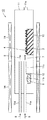
本発明にかかるGaN結晶の製造方法の一実施形態は、図1および図2を参照して、昇華法により成長させたAlN種結晶2の少なくとも一部で形成されているAlN種結晶基板3を用いて、HVPE法によりGaN結晶4を成長させるGaN結晶の製造方法であって、AlN種結晶基板3の反りの曲率半径が5m以上であることを特徴とする。
(Embodiment 1)
An embodiment of a method for producing a GaN crystal according to the present invention is described with reference to FIGS. 1 and 2 in which an AlN
AlNとGaNとは同じ六方晶系であり、格子定数も非常に近いことから、GaN結晶を成長させる種結晶基板としてAlN種結晶基板を用いることにより、種結晶基板上にバッファ層を形成することなく直接GaN結晶をエピタキシャル成長させることが可能となる。また、昇華法により成長させたAlN種結晶で形成されるAlN種結晶基板は、転位密度が低く結晶性が良いため、このAlN種結晶基板上に成長させたGaN結晶も、転位密度が低く結晶性がよくなる。さらに、このAlN種結晶基板は、反りの曲率半径が5m以上と、反りが非常に小さいため、GaN結晶の成長の際に生成する複数のGaN結晶粒の各結晶格子面の面方位が揃い、これらのGaN結晶粒どうしが接合する際に発生する転位が低減され、さらにGaN結晶の転位密度が低減する。なお、本願において、AlN種結晶基板の反りの曲率半径とは、基板の主面の反りの曲率半径をいい、基板の主面における曲率半径を測定することにより算出される。 Since AlN and GaN are the same hexagonal system and have very close lattice constants, a buffer layer is formed on a seed crystal substrate by using an AlN seed crystal substrate as a seed crystal substrate for growing a GaN crystal. It is possible to directly epitaxially grow GaN crystals. Further, since an AlN seed crystal substrate formed of an AlN seed crystal grown by a sublimation method has a low dislocation density and good crystallinity, a GaN crystal grown on this AlN seed crystal substrate also has a low dislocation density. Sexuality improves. Furthermore, since this AlN seed crystal substrate has a very small curvature radius of curvature of 5 m or more, the plane orientation of each crystal lattice plane of the plurality of GaN crystal grains generated during the growth of the GaN crystal is uniform, The dislocations generated when these GaN crystal grains are joined to each other are reduced, and the dislocation density of the GaN crystal is further reduced. In addition, in this application, the curvature radius of the curvature of an AlN seed crystal substrate means the curvature radius of the curvature of the main surface of a substrate, and is computed by measuring the curvature radius in the main surface of a substrate.
本実施形態のGaN結晶の製造方法において、図1に示すAlN種結晶基板3の(0004)面についてのX線回折のロッキングカーブにおける回折強度ピークの半値幅は50arcsec以下であることが好ましい。(0004)面についてのX線回折のロッキングカーブにおける回折強度ピークの半値幅が50arcsec以下となるAlN種結晶基板を構成する各結晶格子面の面方位ずれが小さい結晶性のよいAlN種結晶基板3を用いることにより、結晶性のよいGaN結晶をエピタキシャル成長させることができる。
In the GaN crystal manufacturing method of the present embodiment, the half width of the diffraction intensity peak in the rocking curve of the X-ray diffraction for the (0004) plane of the AlN
また、本実施形態のGaN結晶の製造方法において、図1に示すAlN種結晶基板3の転位密度は1×106cm-2以下であることが好ましい。転位密度が1×106cm-2以下の結晶性の良いAlN種結晶基板3を用いることにより、結晶性のよいGaN結晶をエピタキシャル成長させることができる。ここで、転位密度は、結晶または結晶基板の表面を酸性または塩基性のエッチング液を用いてエッチングしたときに転位に対応して形成されるエッチングピットの単位面積当たりの数を計測することにより算出できる。エッチング液としては、たとえば、350℃のKOH−NaOH混合融液を用いることができる。
In the GaN crystal manufacturing method of this embodiment, the dislocation density of the AlN
また、本実施形態のGaN結晶の製造方法において、図1に示すGaN結晶4の全不純物濃度は1×1018cm-3以下であることが好ましい。HVPE法によれば、結晶成長の際に結晶への不純物混入が少ないため、全不純物濃度が1×1018cm-3以下と純度が高く転位密度が低く結晶性の良いGaN結晶4を成長させることができる。ここで、不純物濃度は、SIMS(二次イオン質量分析)法などにより分析できる。 In the GaN crystal manufacturing method of the present embodiment, the total impurity concentration of the GaN crystal 4 shown in FIG. 1 is preferably 1 × 10 18 cm −3 or less. According to the HVPE method, since the impurities are not mixed into the crystal at the time of crystal growth, the GaN crystal 4 having a high purity such as a total impurity concentration of 1 × 10 18 cm −3 or less and a low dislocation density and good crystallinity is grown. be able to. Here, the impurity concentration can be analyzed by a SIMS (secondary ion mass spectrometry) method or the like.
また、本実施形態のGaN結晶の製造方法において、図1に示すGaN結晶4にn型不純物をドーピングすることができる。GaN結晶4にn型不純物をドーピングすることにより、GaN結晶に導電性を付与することができ、半導体デバイスへの応用上有利である。ここで、n型不純物は、特に制限はないが、HVPE法においてGaN結晶へのドーピングが容易な観点から、シリコンおよび酸素の少なくともひとつであることが好ましい。 Further, in the GaN crystal manufacturing method of the present embodiment, the GaN crystal 4 shown in FIG. 1 can be doped with n-type impurities. By doping the GaN crystal 4 with an n-type impurity, conductivity can be imparted to the GaN crystal, which is advantageous in application to a semiconductor device. Here, the n-type impurity is not particularly limited, but is preferably at least one of silicon and oxygen from the viewpoint of easy doping to the GaN crystal in the HVPE method.
また、本実施形態のGaN結晶の製造方法において、図1に示すAlN種結晶基板3の主面の面積は10cm2以上であることが好ましい。主面の面積が10cm2以上の大きなAlN種結晶基板を用いることにより、大型のGaN結晶を成長させることができる。
In the GaN crystal manufacturing method of the present embodiment, the area of the main surface of the AlN
また、本実施形態のGaN結晶の製造方法において、図3に示すように、AlN種結晶基板3上に開口部30wを有するマスク30を形成し、GaN結晶4をマスク30上でエピタキシャル横方向成長させることが好ましい。かかるELO法によりGaN結晶4を成長させることにより、AlN種結晶基板3の転位3dを引き継ぐことなくGaN結晶4をエピタキシャル成長させることができ、GaN結晶4の転位密度をさらに低減することができる。ここで、マスク30としては、マスク30上でGaN結晶が横方向成長するものであれば特に制限はないが、SiO2、Si3N4などが好ましく用いられる。また、マスク30の開口部30wは、AlN種結晶基板3の転位3dを引き継がないほどに小さいものであれば特に制限はないが、マスクの形成のし易さおよび成長の安定性の観点から、ある程度大きさがある方がよく、開口部の一辺または直径が5μm以上である方が好ましい。また、開口部30wを有するマスクは、CVD法、スパッタリング法などによるマスク材の積層、およびリソグラフィ法などによるマスクのパターニングにより形成される。
In the GaN crystal manufacturing method of the present embodiment, as shown in FIG. 3, a
本実施形態のGaN結晶の製造方法について、以下に詳しく説明する。本実施形態のGaN結晶の製造方法において用いられる種結晶基板は、図1および図2を参照して、昇華法により成長させたAlN種結晶2の少なくとも一部で形成されているAlN種結晶基板3である。
The manufacturing method of the GaN crystal of this embodiment will be described in detail below. The seed crystal substrate used in the GaN crystal manufacturing method of the present embodiment is an AlN seed crystal substrate formed of at least a part of the
本実施形態における昇華法とは、図2を参照して、AlN粉末などのAlN原料1を昇華させた後、再度固化させてAlN結晶(本実施形態におけるAlN種結晶2)を得る方法をいう。昇華法による結晶成長においては、たとえば、図2に示すような高周波加熱方式の縦型の昇華炉20を用いる。この縦型の昇華炉20における反応容器21の中央部には、ガス排気口22eを有する坩堝22が設けられ、坩堝22の周りに坩堝22の内部から外部への通気を確保するように加熱体23が設けられている。また、反応容器21の外側中央部には、加熱体23を加熱するための高周波加熱コイル24が設けられている。さらに、反応容器21の端部には、反応容器21の坩堝22の外部にN2ガス(窒素ガス)を流すためのガス導入口21aおよびガス排気口21eと、坩堝22の下面および上面の温度を測定するための放射温度計25が設けられている。ここで、坩堝22の材料は、特に制限はないが、成長させるAlN結晶(AlN種結晶2)への不純物の混入が少ない観点から、W(タングステン)製であることが好ましい。
The sublimation method in the present embodiment refers to a method of obtaining an AlN crystal (
図2を参照して、上記縦型の昇華炉20を用いて、以下のようにして本発明で用いるAlN種結晶2を作製することができる。坩堝22の下部にAlN粉末などのAlN原料1を収納し、反応容器21内にN2ガスを流しながら、高周波加熱コイル24を用いて加熱体23を加熱することにより坩堝22内の温度を上昇させて、坩堝22のAlN原料1側の温度を、それ以外の部分の温度よりも高く保持することによって、AlN原料1からAlNを昇華させて、坩堝22の上部でAlNを再度固化させて本発明で用いるAlN種結晶2を成長させる。
Referring to FIG. 2,
ここで、AlN種結晶2の成長中は、坩堝22のAlN原料1側の温度は2000℃〜2200℃程度とし、坩堝22の上部(AlN結晶を成長させる部分)の温度をAlN原料1側の温度より1℃〜10℃程度低くすることにより、結晶性のよいAlN種結晶2が得られる。また、結晶成長中も反応容器21内の坩堝22の外側にN2ガスを、ガス分圧が101.3hPa〜1013hPa程度になるように流し続けることにより、AlN種結晶2への不純物の混入を低減することができる。
Here, during the growth of the
なお、坩堝22内部の昇温中は、坩堝22のAlN原料1側の温度よりもそれ以外の部分の温度を高くすることにより、坩堝22内部の不純物をガス排気口21eを通じて除去することができ、AlN種結晶2への不純物の混入をより低減することができる。
During the temperature increase inside the
上記昇華法によって、(0004)面についてのX線のロッキングカーブにおける回折強度ピークの半値幅が50arcsec以下で、転位密度が1×106cm-2以下である結晶性のよいAlN種結晶2が得られる。なお、昇華法の条件を最適化することによって、AlN種結晶の上記回折強度ピークの半値幅を20arcsec〜40arcsec程度、転位密度を1×103cm-2〜1×105cm-2程度まで低減することが可能である。
By the above sublimation method, the
こうして得られたAlN種結晶2の少なくとも一部を切り出して、その表面を研磨することによりAlN種結晶基板3が得られる。ここで、AlN種結晶基板3の厚さを5mm以上とすることにより、反りの曲率半径が5m以上と反りが非常に小さく、回折強度ピークの半値幅が50arcsec以下で、転位密度が1×106cm-2以下と結晶性のよいAlN種結晶基板3が得られる。
The AlN
次に、図1を参照して、上記のようにして得られた反りの曲率半径が5m以上のAlN種結晶基板3を用いて、HVPE法によりGaN結晶4を成長させる。ここで、本実施形態におけるHVPE法とは、図1を参照して、ガリウム原料ガス7としての塩化ガリウムガスと窒素原料ガス8とを反応させてGaN結晶4を成長させる方法をいう。
Next, referring to FIG. 1, GaN crystal 4 is grown by HVPE using AlN
HVPE法によるGaN結晶の成長においては、たとえば、図1に示すようなHVPE装置10を用いる。このHVPE装置10は、反応容器11の内部または外部に、AlN種結晶基板3を載せるためのペディスタル13、ガリウム6を入れるためのガリウムボート12を収納するためのガリウム原料ガス生成室11b、ガリウム原料ガス生成室11bにハロゲン含有ガス5を導入するためのハロゲン含有ガス導入管11a、ガリウム原料ガス生成室11b内で生成したガリウム原料ガス7を反応容器11内に導入するためのガリウム原料ガス導入管11cと、窒素原料ガス8を反応容器11内に導入するための窒素原料ガス導入管11dと、反応後のガスを反応容器11から排気するためのガス排気口11eと、反応容器11を加熱するためのヒータ14が配設されている。
In the growth of a GaN crystal by the HVPE method, for example, an
図1を参照して、上記HVPE装置10を用いて、たとえば、以下のようにしてGaN結晶を作製することができる。まず、反応容器11内に設置されたペディスタル13上に上記AlN種結晶基板3を配置し、ガリウム原料ガス生成室11b内にガリウム6を入れたガリウムボート12を配置する。
With reference to FIG. 1, using the
次に、ハロゲン含有ガス導入管11a、ガリウム原料ガス導入管11cおよび窒素原料ガス導入管11dを通して反応容器11内にキャリアガス(図示せず)を導入しながら、ヒータ14により反応容器11の内部を加熱して、その温度を800℃以上1100℃以下、好ましくは950℃より高く1100℃以下にする。ここで、キャリアガスは、ガリウムと反応せず、GaN結晶の成長に支障をきたさない不活性ガスであれば特に制限はなく、H2ガス(水素ガス)、Arガス(アルゴンガス)、N2ガスなどが好ましく用いられる。
Next, while introducing a carrier gas (not shown) into the reaction vessel 11 through the halogen-containing gas introduction tube 11a, the gallium source
次に、ハロゲン含有ガス5としてHClガス(塩化水素ガス)をキャリアガスとともに、ハロゲン含有ガス導入管11aを通してガリウム原料ガス生成室11bに導入する。ガリウム原料ガス生成室11b内で、ガリウムボート12内のガリウム6とHClガス(ハロゲン含有ガス5)とが反応して、ガリウム原料ガス7であるGaClガス(塩化ガリウムガス)が生成する。このGaClガス(ガリウム原料ガス7)は、ガリウム原料ガス導入管11cを通して反応容器11内に導入される。一方、窒素原料ガス8としてNH3ガス(アンモニアガス)をキャリアガスとともに窒素原料ガス導入管11dを通して反応容器11内に導入する。
Next, HCl gas (hydrogen chloride gas) as the halogen-containing gas 5 is introduced into the gallium source gas generation chamber 11b through the halogen-containing gas introduction tube 11a together with the carrier gas. In the gallium source gas generation chamber 11b, the
このとき、反応容器11内で、GaClガス(ガリウム原料ガス7)とNH3ガス(窒素原料ガス8)とが反応して、AlN種結晶基板3上にGaN結晶が成長する。
At this time, GaCl gas (gallium source gas 7) and NH 3 gas (nitrogen source gas 8) react with each other in the reaction vessel 11 to grow a GaN crystal on the AlN
ここで、ガリウム原料ガス7の分圧(ハロゲン含有ガス5の分圧とほぼ同じ)を50Pa〜1×10⁴Pa程度、窒素原料ガス8の分圧を5×10³Pa〜5×10⁴Pa程度、ガリウム原料ガス7と窒素原料ガス8とのガス比(モル比)を1:10〜1:1000程度、AlN種結晶基板の温度を900℃〜1100℃程度にして、GaN結晶の成長速度を10μm/hr〜30μm/hr程度に調整することにより、結晶性のよい厚いIII族窒化物結晶が得られる。
Here, the partial pressure of the gallium source gas 7 (approximately the same as the partial pressure of the halogen-containing gas 5) is about 50 Pa to 1 × 10 4 Pa, and the partial pressure of the
ここで、ガリウム原料ガス7および窒素原料ガス8とともに反応容器11に導入されるキャリアガスは、ガリウム原料ガスまたは窒素原料ガスの導入量を安定化させるとともに、III族元素原料ガスと窒素原料ガスとの反応性を調節する働きを有する。
Here, the carrier gas introduced into the reaction vessel 11 together with the
(実施形態2)
本発明にかかるGaN結晶基板は、実施形態1の製造方法により得られたGaN結晶の少なくとも一部で形成されているGaN結晶基板である。本実施形態のGaN結晶基板は、転位密度が低く結晶性がよいため、特性のよい半導体デバイスを作製することが可能となる。本実施形態のGaN結晶基板は、実施形態1の製造方法により得られたGaN結晶の少なくとも一部を切り出し、その表面を処理することにより得られる。結晶の表面処理方法には、特に制限はないが、結晶の表面を鏡面に研磨し、この研磨により生じた加工変質層をエッチングにより除去する方法が好ましく行なわれる。
(Embodiment 2)
The GaN crystal substrate according to the present invention is a GaN crystal substrate formed of at least a part of the GaN crystal obtained by the manufacturing method of the first embodiment. Since the GaN crystal substrate of this embodiment has a low dislocation density and good crystallinity, it becomes possible to manufacture a semiconductor device with good characteristics. The GaN crystal substrate of this embodiment is obtained by cutting out at least a part of the GaN crystal obtained by the manufacturing method of
(実施形態3)
本発明にかかる半導体デバイスは、実施形態2のGaN結晶基板を含む半導体デバイスである。半導体デバイスは、実施形態2のGaN結晶基板を含むものであれば特に制限はなく、光デバイス(発光ダイオード、レーザダイオードなど)、電子デバイス(整流器、バイポーラトランジスタ、電界効果トランジスタ、HEMT(High Electron Mobility Transistor;高電子移動度トランジスタ)など)、半導体センサ(温度センサ、圧力センサ、放射線センサ、可視−紫外光検出器など)といった半導体デバイス、またはSAWデバイス(Surface Acoustic Wave Device;表面弾性波素子)、振動子、共振子、発振器、MEMS(Micro-electro-mechanical System;微小電気機械システム)部品、圧電アクチュエータなどが作製可能である。これらの半導体デバイスは、実施形態2のGaN結晶基板の表面上に半導体層や金属層などを積層することなどにより作製することができる。半導体層の積層方法としては、たとえば、MOVPE法、MBE(Molecular Beam Epitaxy;分子線エピタキシャル成長)法などが挙げられる。上記のようなデバイスを製造することができる。金属層の積層方法としては、たとえば、真空蒸着法、スパッタリング法などが挙げられる。
(Embodiment 3)
A semiconductor device according to the present invention is a semiconductor device including the GaN crystal substrate of the second embodiment. The semiconductor device is not particularly limited as long as it includes the GaN crystal substrate of the second embodiment, and is an optical device (light emitting diode, laser diode, etc.), electronic device (rectifier, bipolar transistor, field effect transistor, HEMT (High Electron Mobility). Transistor; high electron mobility transistor)), semiconductor device such as semiconductor sensor (temperature sensor, pressure sensor, radiation sensor, visible-ultraviolet light detector, etc.) or SAW device (Surface Acoustic Wave Device), A vibrator, a resonator, an oscillator, a micro-electro-mechanical system (MEMS) component, a piezoelectric actuator, or the like can be manufactured. These semiconductor devices can be manufactured by stacking a semiconductor layer, a metal layer, or the like on the surface of the GaN crystal substrate of the second embodiment. Examples of the method for laminating the semiconductor layers include MOVPE method, MBE (Molecular Beam Epitaxy) method and the like. Devices as described above can be manufactured. Examples of the metal layer stacking method include a vacuum deposition method and a sputtering method.
(実施例1)
(1−1.昇華法によるAlN種結晶基板の成長)
まず、図2を参照して、昇華法により以下のようにしてAlN種結晶基板2を成長させた。W(タングステン)製の内径5.5cmの坩堝22の下部にAlN原料1としてAlN粉末を収納した。
Example 1
(1-1. Growth of AlN seed crystal substrate by sublimation method)
First, referring to FIG. 2, an AlN
次に、反応容器21内に窒素ガスを流しながら、高周波加熱コイル24を用いて坩堝22内の温度を上昇させた。坩堝22内の昇温中は、坩堝22の上部(AlN種結晶3を成長させる側)の温度を、坩堝22の下部(AlN原料1側)の温度よりも高くして、昇温中に坩堝22内部から放出された不純物を、ガス排気口22eを通じて除去した。
Next, the temperature in the
次に、坩堝22の上部の温度を2100℃、下部の温度を2150℃にして、AlN原料1からAlNを昇華させて、坩堝22の上部で、AlNを再度固化させてAlN種結晶2を成長させた。AlN種結晶成長中も、反応容器21内の坩堝22の外側に窒素ガスを流し続け、反応容器11内の坩堝22の外側のガス分圧が101.3hPa〜1013hPa程度になるように、窒素ガス導入量と窒素ガス排気量とを制御した。上記の結晶成長条件で50時間AlN種結晶2を成長させた後、室温(25℃)まで冷却して、AlN種結晶2を得た。
Next, the temperature of the upper part of the
得られたAlN種結晶2は、結晶の外周部において多結晶化が見られたが、結晶の中心から直径50.8mmの範囲内では、(0004)面についてのX線回折のロッキングカーブにおける回折強度ピークの半値幅50arcsecであり、転位密度は1.0×10⁻⁶cm-2という結晶性のよい低転位密度の単結晶であった。ここで、結晶または結晶基板の転位密度は、それらの表面を350℃のKOH−NaOH混合融液でエッチングしたとき転位に対応して形成されるエッチングピットの単位面積当たりの数を計測することにより算出した。
The obtained
(1−2.AlN種結晶基板の作製)
上記のAlN種結晶2を、AlN種結晶2の結晶成長面(C面)と平行な面でスライスし、また多結晶化した外周部を取り除き、その表面を鏡面に研磨して、直径50.8mm×厚さ400μmのAlN種結晶基板3を得た。このAlN種結晶基板3の主面の反りの曲率半径を触針表面形状測定器により測定したところ、5mであった。また、このAlN種結晶基板3の10μm×10μm角の範囲内におけるAFM(Atomic Force Microscope;原子間力顕微鏡)により観察したRMS(Root Mean Square:平均線から測定曲線までの偏差の二乗を平均した値の平方根)表面粗さは50nm(500Å)以下であった。
(1-2. Preparation of AlN seed crystal substrate)
The above-mentioned
上記のようにして、反りの曲率半径が5mで、主面がC面であり、(0004)面についてのX線回折のロッキングカーブにおける回折強度ピークの半値幅が50arcsecで、転位密度が1.0×106cm-2の、反りが小さく転位密度が低く結晶性がよいAlN種結晶基板3が得られた。
As described above, the curvature radius of the warp is 5 m, the main surface is the C plane, the half width of the diffraction intensity peak in the rocking curve of the X-ray diffraction with respect to the (0004) plane is 50 arcsec, and the dislocation density is 1. An AlN
なお、上記実施例におけるAlN種結晶基板3は、成長させたAlN種結晶2のC面に平行な面でスライスして作製したものであるが、AlN種結晶のスライス面は、C面と平行な面に限定されず、A面、R面、M面またはS面に平行な面、またはこれらの面に対して任意の傾きを有する面とすることができる。
In addition, the AlN
(1−3.HVPE法によるGaN結晶の成長)
次に、図1を参照して、上記のAlN種結晶基板3を用いて、HVPE法によりGaN結晶を成長させた。まず、図1に示すHVPE装置10の石英製の反応容器11(具体的には、石英反応管)内のペディスタル13上に上記のAlN種結晶基板3を配置し、ハロゲン含有ガス導入管11a、ガリウム原料ガス導入管11cおよび窒素原料ガス導入管11dを通して反応容器11内にキャリアガスとして水素ガス(図示せず)を導入しながら、ヒータ14により反応容器11の内部を加熱して、その温度を1050℃とした。
(1-3. Growth of GaN crystal by HVPE method)
Next, referring to FIG. 1, a GaN crystal was grown by the HVPE method using the AlN
次いで、ハロゲン含有ガス5としてHClガスをキャリアガスとともに、ハロゲン含有ガス導入管11aを通してガリウム原料ガス生成室11bに導入した。ガリウム原料ガス生成室11b内で、ガリウムボート12内のガリウム6とHClガス(ハロゲン含有ガス5)とが反応して、ガリウム原料ガス7であるGaClガスが生成され、このGaClガス(ガリウム原料ガス7)が、ガリウム原料ガス導入管11cを通して反応容器11内に導入された。一方、窒素原料ガス8としてNH3ガスをキャリアガスとともに窒素原料ガス導入管11dを通して反応容器11内に導入した。
Next, HCl gas as the halogen-containing gas 5 was introduced into the gallium source gas generation chamber 11b through the halogen-containing gas introduction tube 11a together with the carrier gas. In the gallium source gas generation chamber 11b,
ここで、AlN種結晶基板の温度を1050℃として、GaN結晶の成長速度が50μm/hrとなるようにGaClガスの分圧(HClガスの分圧とほぼ同じ)およびNH3ガスの分圧を調節して、多結晶を形成させることなく厚さ2.0mmのGaN結晶4を成長させた。このGaN結晶4の温度を室温(25℃)まで降下させた後、AlN種結晶基板3上に成長させたGaN結晶4を、反応容器11から取り出した。
Here, the temperature of the AlN seed crystal substrate is set to 1050 ° C., and the partial pressure of GaCl gas (substantially the same as the partial pressure of HCl gas) and the partial pressure of NH 3 gas are set so that the growth rate of the GaN crystal is 50 μm / hr. By adjusting, a GaN crystal 4 having a thickness of 2.0 mm was grown without forming a polycrystal. After the temperature of the GaN crystal 4 was lowered to room temperature (25 ° C.), the GaN crystal 4 grown on the AlN
(1−4.GaN結晶基板の作製)
上記のGaN結晶4を、GaN結晶4の結晶成長面(C面)と平行な面でスライスし、その表面を鏡面に研磨して、直径50.8mm×厚さ400μmのGaN結晶基板を得た。このGaN結晶基板は、転位密度が5×104cm-2で、(0004)面についてのX線回折のロッキングカーブにおける回折強度ピークの半値幅が50arcsecと、転位密度が低く結晶性がよかった。また、このGaN結晶基板のRMS表面粗さは、50nmと良好であった。また、このGaN結晶基板は、透明であり、不純物の混入が少なく純度が高いと考えられる。ここで、このGaN結晶基板についてSIMS法による不純物分析を行なったところ、最も多く混入していた不純物である酸素の濃度は2×1017cm-3であり、混入した全ての不純物の濃度を合計しても1×1018cm-3以下であった。
(1-4. Preparation of GaN crystal substrate)
The GaN crystal 4 was sliced along a plane parallel to the crystal growth surface (C-plane) of the GaN crystal 4, and the surface was polished into a mirror surface to obtain a GaN crystal substrate having a diameter of 50.8 mm and a thickness of 400 μm. . This GaN crystal substrate had a dislocation density of 5 × 10 4 cm −2 , a half-width of a diffraction intensity peak in a rocking curve of X-ray diffraction with respect to the (0004) plane was 50 arcsec, and the dislocation density was low and the crystallinity was good. The RMS surface roughness of this GaN crystal substrate was as good as 50 nm. Further, this GaN crystal substrate is transparent and is considered to have high purity with little contamination of impurities. Here, when the impurity analysis by the SIMS method was performed on the GaN crystal substrate, the concentration of oxygen, which was the most abundant impurity, was 2 × 10 17 cm −3. Even it was 1 × 10 18 cm −3 or less.
(実施例2)
GaN結晶の成長の際に、ガリウム原料ガス7であるGaClガス、窒素原料ガス8であるアンモニアガス(NH3ガス)、キャリアガスである水素ガス(H2ガス)とともに、シリコン含有ガスとしてジクロロシランガス(SiH2Cl2ガス))(図示せず)を、反応容器11内に導入したこと以外は、実施例1と同様にして、不純物としてシリコンを含む厚さ400μmのGaN結晶基板を得た。このGaN結晶基板は、転位密度が5×104cm-2で、(0004)面についてのX線回折のロッキングカーブにおける回折強度ピークの半値幅が40arcsecと、転位密度が低く結晶性がよかった。また、このGaN結晶基板のRMS表面粗さは50nmと良好であった。また、このGaN結晶基板に最も多く混入していた不純物は、シリコン(Si)であり、その濃度は1×1018cm-3であった。
(Example 2)
During the growth of the GaN crystal, dichlorosilane gas as a silicon-containing gas is used together with GaCl gas as a
(比較例1)
GaN結晶の成長の際に、種結晶基板としてHVPE法で作製されたGaN結晶基板(転位密度が5×107cm-2、(0004)面についてのX線回折のロッキングカーブにおける回折強度ピークの半値幅が120arcsec)を用いたこと以外は、実施例1と同様にして、厚さ400μmのGaN結晶基板を得た。このGaN結晶基板は、転位密度が5×107cm-2で、(0004)面についてのX線回折のロッキングカーブにおける回折強度ピークの半値幅が120arcsecと、転位密度が高くなり結晶性が悪かった。
(Comparative Example 1)
During the growth of the GaN crystal, a GaN crystal substrate (dislocation density is 5 × 10 7 cm −2 , the X-ray diffraction rocking curve about the (0004) plane) produced by the HVPE method as a seed crystal substrate. A GaN crystal substrate having a thickness of 400 μm was obtained in the same manner as in Example 1 except that the half width was 120 arcsec. This GaN crystal substrate has a dislocation density of 5 × 10 7 cm −2 and a half-width of a diffraction intensity peak in a rocking curve of X-ray diffraction with respect to the (0004) plane of 120 arcsec, resulting in a high dislocation density and poor crystallinity. It was.
上記のように、昇華法により成長させたAlN種結晶の少なくとも一部で形成され、反りの曲率半径が5m以上であるAlN種結晶基板を用いて、HVPE法によりGaN結晶を成長させることにより、転位密度が低く結晶性のよいGaN結晶が得られる。 As described above, a GaN crystal is grown by the HVPE method using an AlN seed crystal substrate formed of at least a part of the AlN seed crystal grown by the sublimation method and having a curvature radius of curvature of 5 m or more. A GaN crystal having a low dislocation density and good crystallinity can be obtained.
今回開示された実施の形態および実施例はすべての点で例示であって制限的なものではないと考えられるべきである。本発明の範囲は、上記した説明でなくて特許請求の範囲によって示され、特許請求の範囲と均等の意味および範囲内のすべての変更が含まれることが意図される。 It should be understood that the embodiments and examples disclosed herein are illustrative and non-restrictive in every respect. The scope of the present invention is defined by the terms of the claims, rather than the description above, and is intended to include any modifications within the scope and meaning equivalent to the terms of the claims.
1 AlN原料、2 AlN種結晶、3 AlN種結晶基板、3d 転位、4 GaN結晶、5 ハロゲン含有ガス、6 ガリウム、7 ガリウム原料ガス、8 窒素原料ガス、10 HVPE装置、11,21 反応容器、11a ハロゲン含有ガス導入管、11b ガリウム原料ガス生成室、11c ガリウム原料ガス導入管、11d 窒素原料ガス導入管、11e,21e,22e ガス排気口、12 ガリウムボート、13 ペディスタル、14 ヒータ、20 昇華炉、21a ガス導入口、22 坩堝、23 加熱体、24 高周波加熱コイル、25 放射温度計、30 マスク、30w 開口部。 1 AlN raw material, 2 AlN seed crystal, 3 AlN seed crystal substrate, 3d dislocation, 4 GaN crystal, 5 halogen-containing gas, 6 gallium, 7 gallium raw material gas, 8 nitrogen raw material gas, 10 HVPE apparatus, 11, 21 reaction vessel, 11a Halogen-containing gas introduction pipe, 11b Gallium source gas generation chamber, 11c Gallium source gas introduction pipe, 11d Nitrogen source gas introduction pipe, 11e, 21e, 22e Gas exhaust port, 12 Gallium boat, 13 Pedestal, 14 Heater, 20 Sublimation furnace , 21a Gas introduction port, 22 crucible, 23 heating body, 24 high-frequency heating coil, 25 radiation thermometer, 30 mask, 30w opening.
Claims (10)
前記AlN種結晶基板の反りの曲率半径が5m以上であることを特徴とするGaN結晶の製造方法。 A method for producing a GaN crystal, wherein an GaN crystal is grown by an HVPE method using an AlN seed crystal substrate formed of at least a part of an AlN seed crystal grown by a sublimation method,
A method for producing a GaN crystal, wherein the curvature radius of curvature of the AlN seed crystal substrate is 5 m or more.
Priority Applications (1)
| Application Number | Priority Date | Filing Date | Title |
|---|---|---|---|
| JP2006039411A JP2007217227A (en) | 2006-02-16 | 2006-02-16 | GaN crystal manufacturing method, GaN crystal substrate, and semiconductor device |
Applications Claiming Priority (1)
| Application Number | Priority Date | Filing Date | Title |
|---|---|---|---|
| JP2006039411A JP2007217227A (en) | 2006-02-16 | 2006-02-16 | GaN crystal manufacturing method, GaN crystal substrate, and semiconductor device |
Publications (1)
| Publication Number | Publication Date |
|---|---|
| JP2007217227A true JP2007217227A (en) | 2007-08-30 |
Family
ID=38494911
Family Applications (1)
| Application Number | Title | Priority Date | Filing Date |
|---|---|---|---|
| JP2006039411A Pending JP2007217227A (en) | 2006-02-16 | 2006-02-16 | GaN crystal manufacturing method, GaN crystal substrate, and semiconductor device |
Country Status (1)
| Country | Link |
|---|---|
| JP (1) | JP2007217227A (en) |
Cited By (12)
| Publication number | Priority date | Publication date | Assignee | Title |
|---|---|---|---|---|
| WO2009090923A1 (en) * | 2008-01-16 | 2009-07-23 | National University Corporation Tokyo University Of Agriculture And Technology | Laminate and process for producing the laminate |
| WO2010084675A1 (en) * | 2009-01-21 | 2010-07-29 | 日本碍子株式会社 | Group 3b nitride crystal plate |
| US7794541B2 (en) | 2006-03-13 | 2010-09-14 | Tohoku University | Gallium nitride-based material and method of manufacturing the same |
| JP2010222174A (en) * | 2009-03-23 | 2010-10-07 | Nippon Telegr & Teleph Corp <Ntt> | Nitride semiconductor structure |
| JP2011037666A (en) * | 2009-08-11 | 2011-02-24 | Hitachi Cable Ltd | Nitride semiconductor free-standing substrate, method for producing nitride semiconductor free-standing substrate, and nitride semiconductor device |
| JP2012101977A (en) * | 2010-11-10 | 2012-05-31 | Hitachi Cable Ltd | Method for manufacturing nitride semiconductor substrate, and method for manufacturing nitride semiconductor self-standing substrate |
| JP2012182459A (en) * | 2012-03-06 | 2012-09-20 | Nippon Telegr & Teleph Corp <Ntt> | Nitride semiconductor structure |
| WO2013075390A1 (en) * | 2011-11-23 | 2013-05-30 | Gan Zhiyin | Hydride vapor phase epitaxy device |
| JPWO2011108640A1 (en) * | 2010-03-04 | 2013-06-27 | Jx日鉱日石金属株式会社 | Crystal growth apparatus, method for producing nitride compound semiconductor crystal, and nitride compound semiconductor crystal |
| CN106542495A (en) * | 2016-12-12 | 2017-03-29 | 墨宝股份有限公司 | A kind of preparation method of micro-electrical-mechanical system vibration jet actuator |
| WO2020036047A1 (en) * | 2018-08-17 | 2020-02-20 | 三菱ケミカル株式会社 | n-TYPE GaN CRYSTAL, GaN WAFER, AND GaN CRYSTAL, GaN WAFER AND NITRIDE SEMICONDUCTOR DEVICE PRODUCTION METHOD |
| CN115995380A (en) * | 2023-03-22 | 2023-04-21 | 雅安宇焜芯材材料科技有限公司 | System for manufacturing semiconductor |
Citations (3)
| Publication number | Priority date | Publication date | Assignee | Title |
|---|---|---|---|---|
| WO2005031045A2 (en) * | 2003-09-26 | 2005-04-07 | Centre National De La Recherche Scientifique (Cnrs) | Method of producing self-supporting substrates comprising iii-nitrides by means of heteroepitaxy on a sacrificial layer |
| JP2005225693A (en) * | 2004-02-12 | 2005-08-25 | Hitachi Cable Ltd | Manufacturing method of nitride semiconductor |
| JP2006016294A (en) * | 2004-05-31 | 2006-01-19 | Sumitomo Electric Ind Ltd | Method for growing group iii nitride crystal, group iii nitride crystal substrate, and semiconductor device |
-
2006
- 2006-02-16 JP JP2006039411A patent/JP2007217227A/en active Pending
Patent Citations (3)
| Publication number | Priority date | Publication date | Assignee | Title |
|---|---|---|---|---|
| WO2005031045A2 (en) * | 2003-09-26 | 2005-04-07 | Centre National De La Recherche Scientifique (Cnrs) | Method of producing self-supporting substrates comprising iii-nitrides by means of heteroepitaxy on a sacrificial layer |
| JP2005225693A (en) * | 2004-02-12 | 2005-08-25 | Hitachi Cable Ltd | Manufacturing method of nitride semiconductor |
| JP2006016294A (en) * | 2004-05-31 | 2006-01-19 | Sumitomo Electric Ind Ltd | Method for growing group iii nitride crystal, group iii nitride crystal substrate, and semiconductor device |
Cited By (21)
| Publication number | Priority date | Publication date | Assignee | Title |
|---|---|---|---|---|
| US7794541B2 (en) | 2006-03-13 | 2010-09-14 | Tohoku University | Gallium nitride-based material and method of manufacturing the same |
| JP2009190960A (en) * | 2008-01-16 | 2009-08-27 | Tokyo Univ Of Agriculture & Technology | Laminated body and method for producing the same |
| WO2009090923A1 (en) * | 2008-01-16 | 2009-07-23 | National University Corporation Tokyo University Of Agriculture And Technology | Laminate and process for producing the laminate |
| JP5688294B2 (en) * | 2009-01-21 | 2015-03-25 | 日本碍子株式会社 | Group 3B nitride crystal plate |
| WO2010084675A1 (en) * | 2009-01-21 | 2010-07-29 | 日本碍子株式会社 | Group 3b nitride crystal plate |
| JPWO2010084675A1 (en) * | 2009-01-21 | 2012-07-12 | 日本碍子株式会社 | Group 3B nitride crystal plate |
| US9677192B2 (en) | 2009-01-21 | 2017-06-13 | Ngk Insulators, Ltd. | Group 3B nitride crystal substrate |
| JP2010222174A (en) * | 2009-03-23 | 2010-10-07 | Nippon Telegr & Teleph Corp <Ntt> | Nitride semiconductor structure |
| JP2011037666A (en) * | 2009-08-11 | 2011-02-24 | Hitachi Cable Ltd | Nitride semiconductor free-standing substrate, method for producing nitride semiconductor free-standing substrate, and nitride semiconductor device |
| CN101996862A (en) * | 2009-08-11 | 2011-03-30 | 日立电线株式会社 | Nitride semiconductor free-standing substrate, method of manufacturing the same and nitride semiconductor device |
| JPWO2011108640A1 (en) * | 2010-03-04 | 2013-06-27 | Jx日鉱日石金属株式会社 | Crystal growth apparatus, method for producing nitride compound semiconductor crystal, and nitride compound semiconductor crystal |
| JP2012101977A (en) * | 2010-11-10 | 2012-05-31 | Hitachi Cable Ltd | Method for manufacturing nitride semiconductor substrate, and method for manufacturing nitride semiconductor self-standing substrate |
| WO2013075390A1 (en) * | 2011-11-23 | 2013-05-30 | Gan Zhiyin | Hydride vapor phase epitaxy device |
| JP2012182459A (en) * | 2012-03-06 | 2012-09-20 | Nippon Telegr & Teleph Corp <Ntt> | Nitride semiconductor structure |
| CN106542495A (en) * | 2016-12-12 | 2017-03-29 | 墨宝股份有限公司 | A kind of preparation method of micro-electrical-mechanical system vibration jet actuator |
| WO2020036047A1 (en) * | 2018-08-17 | 2020-02-20 | 三菱ケミカル株式会社 | n-TYPE GaN CRYSTAL, GaN WAFER, AND GaN CRYSTAL, GaN WAFER AND NITRIDE SEMICONDUCTOR DEVICE PRODUCTION METHOD |
| JPWO2020036047A1 (en) * | 2018-08-17 | 2021-08-10 | 三菱ケミカル株式会社 | Methods for manufacturing n-type GaN crystals, GaN wafers, and GaN crystals, GaN wafers, and nitride semiconductor devices |
| US11987903B2 (en) | 2018-08-17 | 2024-05-21 | Mitsubishi Chemical Corporation | N-type GaN crystal, GaN wafer, and GaN crystal, GaN wafer and nitride semiconductor device production method |
| JP7552359B2 (en) | 2018-08-17 | 2024-09-18 | 三菱ケミカル株式会社 | N-type GaN crystal, GaN wafer, and methods for manufacturing GaN crystal, GaN wafer, and nitride semiconductor device |
| CN115995380A (en) * | 2023-03-22 | 2023-04-21 | 雅安宇焜芯材材料科技有限公司 | System for manufacturing semiconductor |
| CN115995380B (en) * | 2023-03-22 | 2023-06-20 | 雅安宇焜芯材材料科技有限公司 | System for manufacturing semiconductor |
Similar Documents
| Publication | Publication Date | Title |
|---|---|---|
| JP2007217227A (en) | GaN crystal manufacturing method, GaN crystal substrate, and semiconductor device | |
| CN1148810C (en) | Gallium nitride monocrystal substrate and its manufacturing method | |
| JP5560528B2 (en) | Method for producing group III nitride single crystal ingot and method for producing group III nitride single crystal substrate | |
| JP5018423B2 (en) | Group III nitride semiconductor crystal substrate and semiconductor device | |
| CN104250853B (en) | Group III nitride crystal | |
| JP5068423B2 (en) | Silicon carbide single crystal ingot, silicon carbide single crystal wafer, and manufacturing method thereof | |
| JP6031733B2 (en) | GaN crystal manufacturing method | |
| JP2009126723A (en) | Group III nitride semiconductor crystal growth method, group III nitride semiconductor crystal substrate manufacturing method, and group III nitride semiconductor crystal substrate | |
| JP5509680B2 (en) | Group III nitride crystal and method for producing the same | |
| JP2008133151A (en) | Crystal growth method, crystal substrate, and semiconductor device | |
| JP2011063504A (en) | Nitride semiconductor crystal and method for producing same | |
| JP2007230823A (en) | Method for producing silicon carbide single crystal ingot and silicon carbide single crystal ingot | |
| WO2010007867A1 (en) | Process for producing group iii nitride crystal and group iii nitride crystal | |
| JP4788397B2 (en) | Method for producing group III nitride crystal | |
| JP4408247B2 (en) | Seed crystal for growing silicon carbide single crystal and method for producing silicon carbide single crystal using the same | |
| JP2006225232A (en) | Silicon carbide single crystal manufacturing method, silicon carbide single crystal ingot, silicon carbide single crystal substrate, silicon carbide epitaxial wafer, and thin film epitaxial wafer | |
| JP2006016294A (en) | Method for growing group iii nitride crystal, group iii nitride crystal substrate, and semiconductor device | |
| US20090032907A1 (en) | Method for Producing GaxIn1-xN(0<x>) Crystal Gaxin1-xn(0<x<1) Crystalline Substrate, Method for Producing GaN Crystal, GaN Crystalline Substrate, and Product | |
| JP2006290677A (en) | Nitride-based compound semiconductor crystal manufacturing method and nitride-based compound semiconductor substrate manufacturing method | |
| JP2005343722A (en) | AlN crystal growth method, AlN crystal substrate, and semiconductor device | |
| JP2006021964A (en) | AlN single crystal and growth method thereof | |
| JP2008230868A (en) | Method for growing gallium nitride crystal and gallium nitride crystal substrate | |
| JP2005343704A (en) | Method for producing AlxGayIn1-xyN crystal | |
| JP5440546B2 (en) | Crystal growth method | |
| JP2009292723A (en) | Silicon carbide single crystal ingot with seed crystal, silicon carbide single crystal substrate, silicon carbide epitaxial wafer, and thin film epitaxial wafer |
Legal Events
| Date | Code | Title | Description |
|---|---|---|---|
| A621 | Written request for application examination |
Free format text: JAPANESE INTERMEDIATE CODE: A621 Effective date: 20080924 |
|
| A977 | Report on retrieval |
Free format text: JAPANESE INTERMEDIATE CODE: A971007 Effective date: 20100810 |
|
| A131 | Notification of reasons for refusal |
Free format text: JAPANESE INTERMEDIATE CODE: A131 Effective date: 20100817 |
|
| A02 | Decision of refusal |
Free format text: JAPANESE INTERMEDIATE CODE: A02 Effective date: 20101221 |