JP2007081294A - Nonvolatile semiconductor memory device and manufacturing method thereof - Google Patents
Nonvolatile semiconductor memory device and manufacturing method thereof Download PDFInfo
- Publication number
- JP2007081294A JP2007081294A JP2005270108A JP2005270108A JP2007081294A JP 2007081294 A JP2007081294 A JP 2007081294A JP 2005270108 A JP2005270108 A JP 2005270108A JP 2005270108 A JP2005270108 A JP 2005270108A JP 2007081294 A JP2007081294 A JP 2007081294A
- Authority
- JP
- Japan
- Prior art keywords
- insulating film
- element isolation
- memory device
- charge holding
- semiconductor memory
- Prior art date
- Legal status (The legal status is an assumption and is not a legal conclusion. Google has not performed a legal analysis and makes no representation as to the accuracy of the status listed.)
- Pending
Links
Images


Landscapes
- Element Separation (AREA)
- Semiconductor Memories (AREA)
- Non-Volatile Memory (AREA)
Abstract
Description
この発明は、不揮発性半導体記憶装置およびその製造方法に関する。 The present invention relates to a nonvolatile semiconductor memory device and a manufacturing method thereof.
現在、電気的に書き換え可能な不揮発性半導体記憶装置として、フラッシュメモリが広く知られている。このフラッシュメモリはフローティングゲートと呼ばれる導電性の電荷蓄積領域に電荷を蓄積することによって情報を記憶している。 Currently, flash memories are widely known as electrically rewritable nonvolatile semiconductor memory devices. This flash memory stores information by accumulating charges in a conductive charge accumulation region called a floating gate.
また、電荷蓄積領域として、例えば、酸化膜/窒化膜/酸化膜などの絶縁性の膜を用いたタイプのものも提案されている。電荷蓄積領域として絶縁性の膜を用いると、ソース側、およびドレイン側に、それぞれ独立に電荷を蓄積することができ、1つの素子で2ビットの情報を記憶することが可能となる。 As a charge storage region, for example, a type using an insulating film such as an oxide film / nitride film / oxide film has been proposed. When an insulating film is used as the charge storage region, charges can be stored independently on the source side and the drain side, so that one element can store 2-bit information.
図7A〜図7Cに、第1の従来例として、電荷蓄積領域として絶縁膜を用いるタイプの不揮発性半導体記憶装置を示す。図7Aはこの従来例の平面図であり、図7Bは図7AにおけるB−B’断面図であり、図7Cは図7AにおけるA−A’断面図である。この従来例は、電荷蓄積領域としてゲート電極下に配置された酸化膜/窒化膜/酸化膜の積層構造を持った、いわゆるMONOS(Metal/Oxide/Nitride/Oxide/Silicon)タイプの不揮発性半導体記憶装置を示す(例えば、特許文献1(特開2004−221448号公報)参照)。 7A to 7C show a nonvolatile semiconductor memory device of a type using an insulating film as a charge storage region as a first conventional example. 7A is a plan view of this conventional example, FIG. 7B is a cross-sectional view along B-B ′ in FIG. 7A, and FIG. 7C is a cross-sectional view along A-A ′ in FIG. 7A. This conventional example is a so-called MONOS (Metal / Oxide / Nitride / Oxide / Silicon) type non-volatile semiconductor memory having a stacked structure of oxide film / nitride film / oxide film disposed under a gate electrode as a charge storage region. An apparatus is shown (for example, refer to Patent Document 1 (Japanese Patent Laid-Open No. 2004-221448)).
図7A〜図7Cにおいて、710は半導体基板、711は素子分離絶縁膜、712は下部絶縁膜、713は電荷保持領域となる窒化膜、714は上部絶縁膜、715はゲート電極、716はソース領域、717はドレイン領域である。
7A to 7C,
データの書き込みは、電子を注入し、窒化膜713にトラップさせることにより、この不揮発性半導体記憶装置(メモリセルトランジスタ)のしきい値を増大させることにより行う。具体的には、ゲート電極715に8(V)、ドレイン領域717に5(V)、ソース領域716と半導体基板710に0(V)を印加することによって、ドレイン領域717近傍で発生したホットエレクトロンを窒化膜713のドレイン側に注入しトラップさせることにより書き込みを行う。ここで、この書込み時のソース領域716とドレイン領域717への電圧印加条件を逆にすることによって、図7Bにおける窒化膜713のソース側のみに電子をトラップさせることも可能となる。つまり、1つの素子で2ビットを記憶させることが可能となる。
Data is written by injecting electrons and trapping them in the
一方、データの消去は、ホールをシリコン窒化膜713に注入することによって、上記トラップされた電子を中和させ、メモリセルトランジスタのしきい値を下げることにより行う。具体的には、ゲート電極715に−6(V)、ソース領域716およびドレイン領域717に5(V)を印加し、バンド間トンネリングにより発生したホットホールをシリコン窒化膜713に注入することによって消去を行う。
On the other hand, data is erased by injecting holes into the
次に、図8A〜図8Cに、第2の従来例として、上記第1の従来例のMONOSタイプの不揮発性半導体記憶装置に比べて、2ビットの記憶部分の分離を改善した不揮発性半導体記憶装置を示す(例えば、特許文献2(特開2004−56095号公報)参照)。図8Aはこの従来例の平面図であり、図8Bは図8AにおけるB−B’断面図であり、図8Cは図8AにおけるA−A’断面図である。 Next, as a second conventional example, FIG. 8A to FIG. 8C show a nonvolatile semiconductor memory in which the separation of the storage portion of 2 bits is improved as compared with the MONOS type nonvolatile semiconductor memory device of the first conventional example. An apparatus is shown (for example, refer to Patent Document 2 (Japanese Patent Laid-Open No. 2004-56095)). FIG. 8A is a plan view of this conventional example, FIG. 8B is a B-B ′ sectional view in FIG. 8A, and FIG. 8C is an A-A ′ sectional view in FIG. 8A.
図8A〜図8Cにおいて、810は半導体基板、811は素子分離絶縁膜、812は下部絶縁膜、813は電荷保持領域となる窒化膜、814は上部絶縁膜、815はゲート電極、816はソース領域、817はドレイン領域である。
8A to 8C,
この第2従来例が、前述のMONOSタイプの第1従来例と異なる点は電荷保持領域813がゲート電極815の側壁に対向していることである。図8Bでは、電荷保持領域813がゲート電極815により分離されているので、前述の第1従来例に比べて、2ビットの記憶部分の分離を改善することに成功している。
The second conventional example is different from the first conventional example of the MONOS type in that the
ところで、上述の第1,第2の従来例の不揮発性半導体記憶装置では、電荷保持領域713,813が素子分離絶縁膜711,811上まで延在している。
Incidentally, in the above-described nonvolatile semiconductor memory devices of the first and second conventional examples, the
これについての説明をするために、まず、図7A〜図7Cに示す第1従来例の不揮発性半導体記憶装置の製造方法を説明する。まず、素子分離絶縁膜711を形成した半導体基板710上に下部絶縁膜712、電荷保持領域となる窒化膜713、上部絶縁膜714を順次積層し、続いてポリシリコンを堆積する。その後、レジストを用いてパターニングした後、ポリシリコンをエッチングしゲート電極715を作製する。ここで、上記レジストパターンで上部絶縁膜714、窒化膜713、下部絶縁膜712も同時にエッチングを行う。その後、ソース領域716およびドレイン領域717を形成することによって、図7A〜図7Cに示す第1従来例の不揮発性半導体記憶装置が完成する。
In order to explain this, first, a method of manufacturing the nonvolatile semiconductor memory device of the first conventional example shown in FIGS. 7A to 7C will be described. First, a lower
このように、第1従来例の不揮発性半導体記憶装置では、ゲート電極715を形成する時に、同時に電荷保持領域である窒化膜713も形成されるので、素子分離絶縁膜711上の領域を含むゲート電極715の下方の領域のすべてに電荷蓄積領域713が形成されてしまう。
As described above, in the nonvolatile semiconductor memory device of the first conventional example, when the
ここで、ゲート電極715が素子分離絶縁膜711上まで延在している理由は、ゲート電極715とコンタクトを取る際には、ある程度大きなゲート面積が必要であり、通常そのコンタクト部は素子分離領域上にあるためである。また、図7A〜図7Cに示す不揮発性半導体記憶装置を多数並べてセルアレイ化する際には、ゲート電極715がワードラインとして機能し、1本のゲート電極が複数の素子のゲート電極を兼ねるため、ゲート電極は必然的に素子分離上に延在することとなるためである。
Here, the reason why the
次に、図8A〜図8Cに示す第2従来例の不揮発性半導体記憶装置の製造方法を説明する。まず、素子分離絶縁膜811を形成した半導体基板810上にゲート絶縁膜818を介してゲート電極815を形成する。その後、下部絶縁膜812、窒化膜813を順次積層した後、エッチバックする。その後、上部絶縁膜814を堆積し、ソース領域816およびドレイン領域817を形成することによって、図8A〜図8Cに示す第2従来例の不揮発性半導体記憶装置が完成する。
Next, a method for manufacturing the nonvolatile semiconductor memory device of the second conventional example shown in FIGS. 8A to 8C will be described. First, a
このように、第2従来例の不揮発性半導体記憶装置では、電荷蓄積領域である窒化膜813をエッチバックすることによって作製するので、素子分離絶縁膜811の上方の領域を含むゲート電極815の周りの領域のすべてに電荷蓄積領域813が形成されてしまう。
As described above, since the nonvolatile semiconductor memory device of the second conventional example is manufactured by etching back the
上述の如く、第1,第2の従来例の不揮発性半導体記憶装置では、電荷保持領域713,813が、素子分離絶縁膜711,811上に延在して存在していた。
As described above, in the nonvolatile semiconductor memory devices of the first and second conventional examples, the
書込みの際、電子が注入されるのは、ゲート幅方向において、電荷保持領域713,813のうちの、素子分離絶縁膜711,811で挟まれたチャネル領域上の領域のみである。つまり、電荷保持領域713,813のうちの、素子分離領域711,811上の領域には電子は注入されない。窒化膜からなる電荷保持領域713,813中に注入された電子は、図7Cおよび図8Cに矢印で示したとおり、時間と共に徐々に絶縁膜711,811上の電荷保持領域713,813に移動する。ここで、メモリセルトランジスタのしきい値は、チャネル上の電荷保持領域713,813中に蓄えられている電荷の密度によって決まるので、上記のように素子分離絶縁膜711,811上の電荷保持領域713,813に電荷が移動すると、記憶保持特性が劣化する。なお、図7A〜図7Cに示すMONOSタイプの第1従来例の場合、電荷保持領域713でチャネル方向にも電荷は移動するが、チャネル幅が小さい現在、素子分離絶縁膜711,811上への電荷移動の方が影響が大きい。
そこで、この発明の課題は、記憶保持特性を改善できる不揮発性半導体記憶装置およびその製造方法を提供することにある。 SUMMARY OF THE INVENTION An object of the present invention is to provide a nonvolatile semiconductor memory device that can improve memory retention characteristics and a method for manufacturing the same.
上記課題を解決するため、この発明の不揮発性半導体記憶装置は、半導体基板と、上記半導体基板に埋め込まれた素子分離部と、上記半導体基板内に形成されると共に上記素子分離部によって分離される活性領域と、上記半導体基板上にゲート絶縁膜を介して形成されたゲート電極と、上記半導体基板中に形成されると共に上記ゲート絶縁膜の少なくとも両側に位置するソース領域およびドレイン領域と、上記半導体基板上に形成されると共に上記ゲート電極により電圧が印加される誘電体材料からなる電荷保持部と、を備え、上記電荷保持部は、上記活性領域上に存在するが上記素子分離部上に存在しないことを特徴としている。 In order to solve the above problems, a nonvolatile semiconductor memory device of the present invention includes a semiconductor substrate, an element isolation portion embedded in the semiconductor substrate, and formed in the semiconductor substrate and separated by the element isolation portion. An active region; a gate electrode formed on the semiconductor substrate via a gate insulating film; a source region and a drain region formed in the semiconductor substrate and located on at least both sides of the gate insulating film; and the semiconductor And a charge holding portion formed of a dielectric material to which a voltage is applied by the gate electrode. The charge holding portion exists on the active region but on the element isolation portion. It is characterized by not.
この発明の不揮発性半導体記憶装置では、素子分離部上には電荷保持部が存在しないので、活性領域上の電荷保持部に注入された電荷は、素子分離部上に移動することがなく、チャネル上の電荷保持部に蓄える電荷密度が低下することがない。よって、記憶保持特性が改善する。 In the nonvolatile semiconductor memory device of the present invention, since the charge holding portion does not exist on the element isolation portion, the charge injected into the charge holding portion on the active region does not move onto the element isolation portion, and the channel The charge density stored in the upper charge holding portion does not decrease. Therefore, the memory retention characteristic is improved.
また、一実施形態の不揮発性半導体記憶装置では、上記電荷保持部は、上記ゲート電極とゲート絶縁膜との間に形成されている。 Further, in the nonvolatile semiconductor memory device of one embodiment, the charge holding portion is formed between the gate electrode and the gate insulating film.
この実施形態では、ゲート電極とゲート絶縁膜との間に形成されている電荷保持部のソース側とドレイン側にそれぞれ独立に電荷を保持して、1つの素子で2ビットの情報を記憶することができる。 In this embodiment, charge is independently held on the source side and the drain side of the charge holding portion formed between the gate electrode and the gate insulating film, and 2-bit information is stored in one element. Can do.
また、一実施形態の不揮発性半導体記憶装置は、上記電荷保持部は、すくなくとも一部が上記素子分離部の上端面よりも下方に存在している。 In the nonvolatile semiconductor memory device according to one embodiment, at least a part of the charge holding unit exists below the upper end surface of the element isolation unit.
この実施形態では、素子分離絶縁膜上に電荷保持部が存在しないように作製することが容易になる。 In this embodiment, it is easy to manufacture so that no charge holding portion exists on the element isolation insulating film.
また、一実施形態の不揮発性半導体記憶装置は、上記電荷保持部は、上記ゲート電極の側壁に絶縁膜を介して対向するように配置されている。 In the nonvolatile semiconductor memory device according to one embodiment, the charge holding portion is disposed so as to face the side wall of the gate electrode with an insulating film interposed therebetween.
この実施形態によれば、ゲート電極の側壁を挟む両側に電荷保持部を配置することで、2ビットの記憶部分の分離を確実にできる。 According to this embodiment, by disposing the charge holding portions on both sides of the side wall of the gate electrode, it is possible to reliably separate the 2-bit storage portion.
また、一実施形態の不揮発性半導体記憶装置では、上記電荷保持部は、第1の絶縁膜と第2の絶縁膜とで挟まれている。 In the nonvolatile semiconductor memory device of one embodiment, the charge holding unit is sandwiched between the first insulating film and the second insulating film.
この実施形態によれば、電荷保持部を挟む第1,第2の絶縁膜によって、電荷保持部から電荷が洩れるのを抑制でき、良好な記憶保持特性を得ることができる。 According to this embodiment, the first and second insulating films sandwiching the charge holding portion can suppress the leakage of charges from the charge holding portion, and can obtain good memory holding characteristics.
また、一実施形態の不揮発性半導体記憶装置の製造方法では、半導体基板に素子分離用の溝を形成する工程と、
上記溝を素子分離絶縁膜で埋め込む工程と、
上記半導体基板上に絶縁膜を介して電荷保持部を形成する工程と、
上記電荷保持部のうち、上記素子分離絶縁膜上に存在する部分を除去する工程と、
上記電荷保持部上にゲート電極を形成する工程と、
上記ゲート電極をマスクとして上記半導体基板中に不純物を注入し、ソース領域およびドレイン領域を形成する工程とを備える。
In one embodiment of the method for manufacturing a nonvolatile semiconductor memory device, the step of forming a groove for element isolation in a semiconductor substrate;
Filling the trench with an element isolation insulating film;
Forming a charge holding portion on the semiconductor substrate via an insulating film;
Removing the portion of the charge holding portion existing on the element isolation insulating film;
Forming a gate electrode on the charge holding portion;
A step of implanting impurities into the semiconductor substrate using the gate electrode as a mask to form a source region and a drain region.
この実施形態の製造方法によれば、上記の工程を経ることによって、素子分離絶縁膜上に電荷保持部が存在しない不揮発性半導体記憶装置を良好に作製することが可能となる。 According to the manufacturing method of this embodiment, it is possible to satisfactorily manufacture a nonvolatile semiconductor memory device having no charge holding portion on the element isolation insulating film through the above-described steps.
また、一実施形態の不揮発性半導体記憶装置の製造方法は、半導体基板上に絶縁膜を介して電荷保持部となる誘電体膜を形成する工程と、
上記誘電体膜を貫通して上記半導体基板に素子分離用の溝を形成する工程と、
上記溝を素子分離絶縁膜で埋め込む工程と、
上記電荷保持部上にゲート電極を形成する工程と、
上記ゲート電極をマスクとして上記半導体基板中に不純物を注入し、ソース領域およびドレイン領域を形成する工程とを備える。
According to one embodiment, a method for manufacturing a nonvolatile semiconductor memory device includes a step of forming a dielectric film serving as a charge holding portion on a semiconductor substrate via an insulating film;
Forming a groove for element isolation in the semiconductor substrate through the dielectric film;
Filling the trench with an element isolation insulating film;
Forming a gate electrode on the charge holding portion;
A step of implanting impurities into the semiconductor substrate using the gate electrode as a mask to form a source region and a drain region.
この実施形態の製造方法によれば、上記の工程を経ることによって、素子分離絶縁膜上に電荷保持部が存在しない不揮発性半導体記憶装置を良好に作製することが可能となる。 According to the manufacturing method of this embodiment, it is possible to satisfactorily manufacture a nonvolatile semiconductor memory device having no charge holding portion on the element isolation insulating film through the above-described steps.
また、一実施形態の不揮発性半導体記憶装置の製造方法は、半導体基板に素子分離用の溝を形成する工程と、
上記溝を素子分離絶縁膜で埋め込む工程と、
上記半導体基板上にゲート絶縁膜を形成する工程と、
上記ゲート絶縁膜上にゲート電極を形成する工程と、
上記ゲート電極の側壁に絶縁膜を介して対向するように電荷保持部を形成する工程と、
上記電荷保持部のうち、上記素子分離絶縁膜上の部分を除去する工程と、
上記ゲート電極および上記電荷保持部をマスクとして上記半導体基板中に不純物を注入し、ソース領域およびドレイン領域を形成する工程とを備える。
According to one embodiment, a method for manufacturing a nonvolatile semiconductor memory device includes a step of forming a groove for element isolation in a semiconductor substrate,
Filling the trench with an element isolation insulating film;
Forming a gate insulating film on the semiconductor substrate;
Forming a gate electrode on the gate insulating film;
Forming a charge holding portion so as to face the side wall of the gate electrode through an insulating film;
Removing the portion of the charge retention portion on the element isolation insulating film;
A step of implanting impurities into the semiconductor substrate using the gate electrode and the charge holding portion as a mask to form a source region and a drain region.
この実施形態の製造方法によれば、上記の工程を経ることによって、素子分離絶縁膜上に電荷保持部が存在しない不揮発性半導体記憶装置を良好に作製することが可能となる。 According to the manufacturing method of this embodiment, it is possible to satisfactorily manufacture a nonvolatile semiconductor memory device having no charge holding portion on the element isolation insulating film through the above-described steps.
また、一実施形態の携帯電子機器は、上記不揮発性半導体記憶装置を備える。 Moreover, the portable electronic device of one Embodiment is provided with the said non-volatile semiconductor memory device.
この実施形態によれば、上記不揮発性半導体記憶装置を備えることによって、記憶保持特性の優れた携帯電子機器を実現することが可能となる。 According to this embodiment, by providing the nonvolatile semiconductor memory device, a portable electronic device having excellent memory retention characteristics can be realized.
この発明の不揮発性半導体記憶装置よれば、素子分離部上には電荷保持部が存在しないので、活性領域上の電荷保持部に注入された電荷は、素子分離部上に移動することがなく、チャネル上の電荷保持部に蓄える電荷密度が低下することがない。よって、記憶保持特性が改善する。 According to the nonvolatile semiconductor memory device of the present invention, since the charge holding portion does not exist on the element isolation portion, the charge injected into the charge holding portion on the active region does not move onto the element isolation portion, The charge density stored in the charge holding portion on the channel does not decrease. Therefore, the memory retention characteristic is improved.
以下、この発明を図示の実施の形態により詳細に説明する。 Hereinafter, the present invention will be described in detail with reference to the illustrated embodiments.
(第1の実施の形態)
図1A〜図1Cに、この発明の不揮発性半導体記憶装置の第1実施形態を示す。図1Aは第1実施形態の平面図であり、図1Bは図1AにおけるB−B’断面図であり、図1Cは図1AにおけるA−A’断面図である。
(First embodiment)
1A to 1C show a nonvolatile semiconductor memory device according to a first embodiment of the present invention. 1A is a plan view of the first embodiment, FIG. 1B is a BB ′ sectional view in FIG. 1A, and FIG. 1C is an AA ′ sectional view in FIG. 1A.
図1Cに示すように、この第1実施形態は、半導体基板10と、この半導体基板10に埋め込まれた素子分離部としての素子分離絶縁膜11と、素子分離絶縁膜11間に形成された第2の絶縁膜としての下部絶縁膜12を有する。また、素子分離絶縁膜11間の下部絶縁膜12上にシリコン窒化膜で作製された電荷保持部13が形成されている。この電荷保持部13上には第1の絶縁膜としての上部絶縁膜14が形成され、この上部絶縁膜14上にはゲート電極15が形成されている。
As shown in FIG. 1C, the first embodiment includes a
図1A,図1Bに示すように、上記半導体基板10にはソース領域16とドレイン領域17が形成されている。このソース領域16とドレイン領域17の間はチャネル領域19となる。ソース領域16とドレイン領域17とチャネル領域19が活性領域を構成している。ここで、電荷保持部13は、上記活性領域上に存在するが素子分離部としての素子分離絶縁膜11上に存在していない。
As shown in FIGS. 1A and 1B, a
したがって、ゲート電極15下の電荷保持部13のソース側とドレイン側にそれぞれ独立に電荷を保持して、1つの素子で2ビットの情報を記憶するに際し、活性領域上の電荷保持部13に注入された電荷は、素子分離部としての素子分離絶縁膜11上に移動することがない。よって、チャネル領域19上の電荷保持部13に蓄える電荷密度が低下することがないので、記憶保持特性を改善できる。
Therefore, when storing charges independently on the source side and the drain side of the
半導体基板10は、例えば、P型シリコン基板、SOI(シリコン・オン・インシュレータ)基板などを用いることができる。また、素子分離絶縁膜11は、STI(シャロウ・トレンチ・アイソレーション)により形成されたシリコン酸化膜、またはLOCOS(ローカル・オキシデーション・オブ・シリコン)法により形成されたシリコン酸化膜などにより形成されている。
As the
また、素子分離部としての素子分離絶縁膜11の上端11Aは電荷保持部13の上端13Aよりも上方に位置している。もしくは、素子分離絶縁膜11の上端11Aは、電荷保持部13の上端13Aと略同じ高さに位置している。このことにより、活性領域上に存在するが素子分離絶縁膜11上に存在していない電荷保持部13を有する不揮発性半導体記憶装置を良好に製造することが可能となる。
Further, the
また、下部絶縁膜12は、例えば、膜厚1nm〜10nm程度のシリコン酸化膜などから形成されていて、ポテンシャルバリアとして機能する。電荷保持部13は、その内部に電荷を保持するためのトラップ準位などを有し、電荷を保持する領域として機能する。この電荷保持部13は、例えば、膜厚1nm〜15nm程度の窒化膜などにより形成されている。また、上部絶縁膜14は、例えば、膜厚1nm〜20nm程度のシリコン酸化膜などから形成されていて、ポテンシャルバリアとして機能する。したがって、この第1実施形態では、電荷保持部13を挟む上部絶縁膜14と下部絶縁膜12によって、電荷保持部13から電荷が洩れるのを抑制でき、良好な記憶保持特性を得ることができる。
The lower insulating
また、ゲート電極15は、例えば、N型にドープされた多結晶シリコンなどを用いることができる。また、ソース領域16およびドレイン領域17は、例えば、高濃度にN型不純物がドープされた領域より形成されている。
The
上述の如く、この第1実施形態は、従来の不揮発性半導体記憶装置と異なり、素子分離絶縁膜11上に電荷保持部13が存在していない。素子分離絶縁膜11上に電荷保持部13が存在しないことによって、書込み動作によってチャネル領域19の上方の電荷保持領域13に注入された電子が素子分離絶縁膜11上に移動することはない。したがって、この第1実施形態では、従来の記憶保持特性劣化の原因である素子分離絶縁膜上の電荷保持領域への電荷移動を防止できるので、記憶保持特性を改善できる。
As described above, in the first embodiment, unlike the conventional nonvolatile semiconductor memory device, the
(製造方法)
次に、図2A〜図2Dを参照して、上記第1実施形態の不揮発性半導体記憶装置の製造方法を説明する。なお、図2A〜図2Dは、ゲート幅方向の断面図である。
(Production method)
Next, with reference to FIGS. 2A to 2D, a method for manufacturing the nonvolatile semiconductor memory device of the first embodiment will be described. 2A to 2D are cross-sectional views in the gate width direction.
まず、図2Aに示すように、P型の不純物がドープされたシリコン基板である半導体基板10上に熱酸化によって、下部絶縁膜12となる膜厚1nm〜10nmのシリコン酸化膜112を形成した後、CVD(化学気相成長)法によって、電荷保持部13となる膜厚1nm〜15nmのシリコン窒化膜113を形成する。
First, as shown in FIG. 2A, after a
次に、図2Bに示すように、レジスト(図示せず)を用いて、堆積膜(シリコン酸化膜112と窒化膜113)を活性領域の形状にパターニングし、RIE(反応性イオンエッチング)を行うことにより、堆積膜(シリコン酸化膜112とシリコン窒化膜113)を順次エッチングする。これにより、下部絶縁膜12と電荷保持部13を形成する。
Next, as shown in FIG. 2B, using a resist (not shown), the deposited films (
続いて、同一パターンのレジストでシリコン基板10をエッチングし、シリコン基板である半導体基板10に素子分離用の溝117を形成する。その後、CVD法によって、上記溝117を埋め込むように、素子分離絶縁膜11となる膜厚200nmのシリコン酸化膜119を堆積させる。
Subsequently, the
次に、図2Cに示すように、CMP(化学的機械的研磨)プロセスによって、素子分離絶縁膜11となるシリコン絶縁膜119を平坦化し、電荷保持部13の上端13A付近まで研磨を行う。その後、フッ酸により電荷保持領域13上のシリコン絶縁膜119を除去し、素子分離絶縁膜11を形成する。ここで、シリコン基板である半導体基板10の表面部の素子分離絶縁膜11で挟まれる領域がチャネル領域19となる。
Next, as shown in FIG. 2C, the
次に、図2Dに示すように、CVD法により、上部絶縁膜14となる膜厚1nm〜20nmのシリコン酸化膜と、N型にドープされた多結晶シリコンを順次堆積し、レジストを用いてパターニングしたのち、RIEにより上記多結晶シリコンをエッチングし、上部絶縁膜14とゲート電極15を形成する。その後、上記ゲート電極15をマスクとして、シリコン基板である半導体基板10に例えば砒素イオンを注入し、ソース領域16およびドレイン領域17を形成する。これにより、図1A〜図1Cに示す不揮発性半導体記憶装置が完成する。
Next, as shown in FIG. 2D, a silicon oxide film having a film thickness of 1 nm to 20 nm to be the upper insulating
図2Bを参照して説明したように、電荷保持部13となる窒化膜113を形成した後、素子分離のための溝117を形成するレジストパターンで、上記窒化膜113をエッチングして、電荷保持部13を形成する。これにより、素子分離絶縁膜11上には電荷保持部13が延在しない。よって、電荷保持部13の電荷が素子分離領域上へ移動するという記憶保持特性の劣化の原因となる現象を回避でき、記憶保持特性の向上を図ることができる。
As described with reference to FIG. 2B, after forming the
(第2の実施の形態)
次に、図3A〜図3Dを順に参照して、この発明の第2実施形態としての不揮発性半導体記憶装置の製造方法を説明する。なお、図3A〜図3Dは、図1におけるA−A’断面図である図1Cと同様に、ゲート幅方向の断面図である。
(Second embodiment)
Next, with reference to FIGS. 3A to 3D in order, a method for manufacturing the nonvolatile semiconductor memory device according to the second embodiment of the invention will be described. 3A to 3D are cross-sectional views in the gate width direction, similar to FIG. 1C, which is a cross-sectional view along AA ′ in FIG.
この第2実施形態の製造方法では、まず、図3Aに示すように、P型の不純物がドープされたシリコン基板30上に熱酸化によって膜厚10nm程度の酸化膜39を形成した後、CVD(化学気相成長)法によって、CMP(化学的機械的研磨)ストッパとなる膜厚100nm程度の窒化膜40を形成する。その後、レジスト(図示せず)を用いて、上記窒化膜40をパターニングし、RIE(反応性イオンエッチング)により上記窒化膜40をエッチングする。続いて、上記窒化膜40をマスクとして、シリコン基板30をエッチングし、シリコン基板30中に素子分離領域となる溝131を形成する。その後、CVD法によって、溝131を埋め込むようにシリコン酸化膜を膜厚200nmの厚さで堆積させる。その後、上記窒化膜40をストッパとして、CMPプロセスによって、上記シリコン酸化膜の不要部分を除去し、素子分離絶縁膜31を形成する。
In the manufacturing method of the second embodiment, as shown in FIG. 3A, first, an
ここで、この素子分離絶縁膜31の上端31Aを、シリコン基板30の上端面30Aよりも3nm〜100nmだけ上方に延在させて、この上端31Aを後に形成する電荷保持部33の主要部33Aよりも上方に存在させるようにする。ここで、シリコン基板30の表面の素子分離部である素子分離絶縁膜31で挟まれる領域がチャネル領域39となる。
Here, the
次に、図3Bに示すように、リン酸液を用いて窒化膜40を除去し、熱酸化により下部絶縁膜12となる膜厚1nm〜10nmのシリコン酸化膜132を形成する。その後、CVDにより電荷保持部34となる膜厚1nm〜15nmのシリコン窒化膜133を形成する。その後、CVDにより上部絶縁膜34となるシリコン酸化膜134を膜厚200nm程度堆積させる。
Next, as shown in FIG. 3B, the
次に、図3Cに示すように、CMPプロセスによって、素子分離絶縁膜31上のシリコン酸化膜132とシリコン窒化膜133を除去すると共に、シリコン酸化膜134の膜厚が1nm〜20nmになるまで研磨を行い、上部絶縁膜34を形成する。ここで、チャネル領域39上のシリコン窒化膜133は、素子分離絶縁膜31上の窒化膜133よりも下方に形成されているので、上記CMPプロセスでは、チャネル領域39上の電荷保持部33となるシリコン窒化膜133は研磨されない。
Next, as shown in FIG. 3C, the
また、ここで、上記CMPプロセスでは、上部絶縁膜34の膜厚を制御し難い場合は、CMPプロセスにより、素子分離部である素子分離絶縁膜31上のシリコン窒化膜133を除去した後、シリコン酸化膜132を一端フッ酸で除去した後、CVDにより窒化膜133上に上部絶縁膜34となるシリコン酸化膜を堆積させてもよい。
Here, if it is difficult to control the film thickness of the upper insulating
次に、図3Dに示すように、CVDによりN型にドープされた多結晶シリコンを堆積し、レジストを用いてパターニングしたのち、RIEにより上記多結晶シリコンをエッチングし、ゲート電極35を形成する。その後、上記ゲート電極35をマスクとして、例えば、砒素イオンを注入し、ソース領域(図示せず)およびドレイン領域(図示せず)を形成することによって、不揮発性半導体記憶装置が完成する。
Next, as shown in FIG. 3D, N-type doped polycrystalline silicon is deposited by CVD, patterned using a resist, and then etched by RIE to form a
この第2実施形態の製造方法で作製した不揮発性半導体記憶装置によれば、図3Cを参照して説明したように、CMPプロセスによって素子分離絶縁膜31上のシリコン窒化膜133を除去している。よって、素子分離絶縁膜31上に電荷保持部33が残らないので、従来のように、素子分離絶縁膜上の電荷保持部へ電荷が移動するという記憶保持特性の劣化の原因となる現象を回避でき、記憶保持特性の向上を図れる。
According to the nonvolatile semiconductor memory device manufactured by the manufacturing method of the second embodiment, as described with reference to FIG. 3C, the
(第3の実施の形態)
次に、図4A〜図4Cを参照して、この発明の第3実施形態としての不揮発性半導体記憶装置を説明する。なお、図4Aは第3実施形態の平面図であり、図4Bは図4AにおけるB−B’断面図であり、図4Cは図4AにおけるA−A’断面図である。
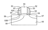
(Third embodiment)
Next, with reference to FIGS. 4A to 4C, a non-volatile semiconductor memory device as a third embodiment of the present invention will be described. 4A is a plan view of the third embodiment, FIG. 4B is a BB ′ sectional view in FIG. 4A, and FIG. 4C is an AA ′ sectional view in FIG. 4A.
図4Bに示すように、この第3実施形態は、半導体基板50と、半導体基板50に形成されたソース領域56およびドレイン領域57と、半導体基板50上に形成されたゲート電極55を有する。ソース領域56とドレイン領域57との間はチャネル領域59となっており、チャネル領域59とゲート電極55との間にはシリコン酸化膜で作製されたゲート絶縁膜58が形成されている。ゲート絶縁膜58およびゲート電極55の両側壁を挟むように第2の絶縁膜52が形成されている。また、この第2の絶縁膜52の外側で、ゲート絶縁膜58の両側壁を挟むように、シリコン窒化膜で作製された電荷保持部53が形成されている。また、上記第2の絶縁膜52とで電荷保持部53を挟むように、第1の絶縁膜54が形成されている。なお、第2の絶縁膜52は、ゲート電極55の側壁に沿って延在している第1部分52Aと、ゲート絶縁膜58と第1の絶縁膜54との間に延在している第2部分52Bとを有する。
As shown in FIG. 4B, the third embodiment includes a
また、図4Cに示すように、この第3実施形態は、第2の絶縁膜52の両側で半導体基板50に埋め込まれた素子分離部としての素子分離絶縁膜51を有する。また、この第3実施形態は、図4Bに示すように、半導体基板50上にシリコン酸化膜で作製されたゲート絶縁膜58を有し、このゲート絶縁膜58上にゲート電極55が形成されている。
As shown in FIG. 4C, the third embodiment has element
半導体基板50としては、例えば、P型シリコン基板、SOI(シリコン・オン・インシュレータ)基板などを用いることができる。また、素子分離絶縁膜51は、STI(シャロウ・トレンチ・アイソレーション)により形成されたシリコン酸化膜、またはLOCOS(ローカル・オキシデーション・オブ・シリコン)により形成されたシリコン酸化膜などにより形成されている。また、ゲート絶縁膜58は、一例として、膜厚1nm〜10nmのシリコン酸化膜から形成されている。また、第2の絶縁膜52は、例えば、膜厚1nm〜10nm程度のシリコン酸化膜などから形成され、ポテンシャルバリアとして機能する。
As the
また、電荷保持部53は、その内部に電荷を保持するためのトラップ準位などを有し、例えば膜厚1nm〜15nm程度のシリコン窒化膜などにより形成され、電荷を保持する領域として機能する。また、第1の絶縁膜54は、例えば、膜厚1nm〜20nm程度のシリコン酸化膜などから形成され、ポテンシャルバリアとして機能する。また、ゲート電極55としては、例えば、N型にドープされた多結晶シリコンなどを用いることができる。また、上述の如く、第2の絶縁膜52、電荷保持部53、第1の絶縁膜54は、ゲート電極55の側壁に形成されている。また、ソース領域56およびドレイン領域57は、例えば、高濃度にN型不純物がドープされた領域で形成されている。
The
この第3実施形態の不揮発性半導体記憶装置が、従来の不揮発性半導体記憶装置と異なる点は、素子分離部である素子分離絶縁膜51上に電荷保持部53が存在しない点である。この第3実施形態では、素子分離絶縁膜51上に電荷保持部53が存在しないので、書込み動作によってチャネル領域59の上方の電荷保持部53に注入された電子は、チャネル領域59の上方に存在するが素子分離絶縁膜51上には存在しない。つまり、この第3実施形態によれば、従来例で記憶保持特性劣化の原因となっていた素子分離絶縁膜上の電荷保持領域への電荷移動を防止できるので、記憶保持特性を改善できる。
The non-volatile semiconductor memory device of the third embodiment is different from the conventional non-volatile semiconductor memory device in that the
次に、図5A〜図5D,図6A〜図6Dを順に参照して、上記第3実施形態の不揮発性半導体記憶装置の製造方法を説明する。なお、図5A〜図5Dは平面図であり、図6A〜図6Dはそれぞれ図5A〜図5DのA−A’断面図である。 Next, with reference to FIGS. 5A to 5D and FIGS. 6A to 6D in order, a method for manufacturing the nonvolatile semiconductor memory device according to the third embodiment will be described. 5A to 5D are plan views, and FIGS. 6A to 6D are A-A ′ cross-sectional views of FIGS. 5A to 5D, respectively.
まず、図5A,図6Aに示すように、P型の不純物がドープされたシリコン基板50上に熱酸化によって膜厚10nm程度のシリコン酸化膜69を形成した後、CVD法によって、CMPストッパとなる膜厚100nm程度の窒化膜70を形成する。その後、レジスト(図示せず)を用いてシリコン窒化膜70をパターニングし、さらに、RIE(反応性イオンエッチング)により上記シリコン窒化膜70をエッチングする。
First, as shown in FIGS. 5A and 6A, a silicon oxide film 69 having a thickness of about 10 nm is formed on a
続いて、上記シリコン窒化膜70をマスクとして、シリコン基板50をエッチングし、シリコン基板50中に素子分離領域となる溝151を形成する。その後、CVDによって、上記溝151を埋め込むようにシリコン酸化膜(図示せず)を膜厚200nmの厚さで堆積させる。その後、上記窒化膜70をストッパとして、CMPプロセスによって、上記シリコン酸化膜の不要部分を除去し、素子分離絶縁膜51を形成する。ここで、シリコン基板50表面部の素子分離絶縁膜51で挟まれる領域がチャネル領域59となる。
Subsequently, using the
次に、図5B,図6Bに示すように、リン酸液を用いて窒化膜70を除去し、次に、フッ酸により酸化膜69を除去する。その後、熱酸化によりゲート絶縁膜58となる膜厚1nm〜10nmのシリコン酸化膜(図示せず)を形成する。次に、CVDによりN型にドープされた多結晶シリコンを堆積し、レジストを用いてパターニングしたのち、RIEにより上記多結晶シリコンをエッチングし、ゲート電極55を形成する。その後、熱酸化あるいはCVDにより第2の絶縁膜52となる膜厚1nm〜10nmのシリコン酸化膜152を堆積する。その後、第2絶縁膜52となるシリコン酸化膜152上にCVDにより電荷保持部53となるシリコン窒化膜153を膜厚1nm〜15nm程度堆積する。
Next, as shown in FIGS. 5B and 6B, the
その後、RIEにより電荷保持部53となるシリコン窒化膜153、および第2絶縁膜52となるシリコン酸化膜152をエッチバックすることによって、ゲート電極55の側壁に電荷保持部53となるシリコン窒化膜153が形成される。続いて、全面にCVDにより第1の絶縁膜54となる膜厚1nm〜20nmのシリコン酸化膜154を堆積する。その後、上記ゲート電極55および第2絶縁膜52となるシリコン酸化膜152、電荷保持部53となるシリコン窒化膜153、第1絶縁膜54となるシリコン酸化膜154をマスクとして、例えば砒素イオンを注入し、ソース領域56およびドレイン領域57を形成する。その後、エッチバックすることによって、ゲート電極55の側壁に第1絶縁膜54となるシリコン酸化膜154を形成する。
After that, the
次に、図5C,図6Cに示すように、チャネル部分をレジスト71でパターニングした後、素子分離絶縁膜51上の第2絶縁膜52となるシリコン酸化膜152、電荷保持部53となるシリコン窒化膜153、第1絶縁膜54となるシリコン酸化膜154をエッチングする。ここで、レジストパターン71をパターニングする際、アライメントずれを考慮して、素子分離部である素子分離絶縁膜51の端からアライメントずれ分だけ、活性領域上の電荷保持部53となるシリコン窒化膜153がエッチングされるようにレジストパターン71をパターニングしてもよい。
Next, as shown in FIGS. 5C and 6C, after the channel portion is patterned with a resist 71, the
このようにすると、アライメントずれが発生した場合においても、電荷保持部53が素子分離絶縁膜51上まで延在することを防止できる。また、チャネル領域59上の端部において電荷保持部53となるシリコン窒化膜153を除去した場合、除去した部分の下のチャネル領域59の電流量は、書込み消去によって変化させることはできなくなるが、書き込み状態および消去状態における読み出し時に一定の電流が加算されるだけなので、動作上の問題は特に生じない。
By doing so, it is possible to prevent the
次に、上記エッチングの後、図5D,図6Dに示すように、レジストパターン71を除去することによって、図4A〜図4Cに示した第3実施形態の不揮発性半導体記憶装置が完成する。
Next, after the etching, as shown in FIGS. 5D and 6D, the resist
上記で説明したとおり、素子分離絶縁膜51上の電荷保持部53をレジスト71でパターニングしたあと、エッチングにより除去することによって、素子分離絶縁膜51上に電荷保持部53が存在しなくなる。よって、この第3実施形態によれば、従来例で記憶保持特性の劣化の原因となっていた素子分離部上の電荷保持部への電荷の移動を回避でき、記憶保持特性を向上できる。
As described above, the
尚、上述の実施形態では、電荷保持部をシリコン窒化膜で作製したが、電荷保持部はシリコン窒化膜以外の他の窒化膜で作製してもよく、他の誘電体材料(例えば、シリコン酸化膜、シリコン酸窒化膜、ポリイミド系有機膜など)で作製してもよい。また、上述の実施形態の不揮発性半導体記憶装置を備える携帯電子機器によれば、記憶保持特性の優れた携帯電子機器を実現できる。 In the above-described embodiment, the charge holding portion is made of a silicon nitride film. However, the charge holding portion may be made of a nitride film other than the silicon nitride film, and other dielectric materials (for example, silicon oxide Film, silicon oxynitride film, polyimide organic film, etc.). Further, according to the portable electronic device including the nonvolatile semiconductor memory device of the above-described embodiment, a portable electronic device having excellent memory retention characteristics can be realized.
10,30…半導体基板
11,31…素子分離絶縁膜
12,32…下部絶縁膜
13,33…電荷保持部
14,34…上部絶縁膜
15,35…ゲート電極
16…ソース領域
17…ドレイン領域
19,39…チャネル領域
50…半導体基板
51…素子分離絶縁膜
52…第2の絶縁膜
53…電荷保持部
54…第1の絶縁膜
55…ゲート電極
59…チャネル領域
71…レジスト
DESCRIPTION OF
Claims (9)
上記半導体基板に埋め込まれた素子分離部と、
上記半導体基板内に形成されると共に上記素子分離部によって分離される活性領域と、
上記半導体基板上にゲート絶縁膜を介して形成されたゲート電極と、
上記半導体基板中に形成されると共に上記ゲート絶縁膜の少なくとも両側に位置するソース領域およびドレイン領域と、
上記半導体基板上に形成されると共に上記ゲート電極により電圧が印加される誘電体材料からなる電荷保持部と、
を備え、
上記電荷保持部は、
上記活性領域上に存在するが上記素子分離部上に存在しないことを特徴とする不揮発性半導体記憶装置。 A semiconductor substrate;
An element isolation portion embedded in the semiconductor substrate;
An active region formed in the semiconductor substrate and separated by the element isolation part;
A gate electrode formed on the semiconductor substrate via a gate insulating film;
A source region and a drain region formed in the semiconductor substrate and located on at least both sides of the gate insulating film;
A charge holding portion made of a dielectric material formed on the semiconductor substrate and applied with a voltage by the gate electrode;
With
The charge holding portion is
A non-volatile semiconductor memory device that exists on the active region but does not exist on the element isolation portion.
上記電荷保持部は、上記ゲート電極とゲート絶縁膜との間に形成されていることを特徴とする不揮発性半導体記憶装置。 The nonvolatile semiconductor memory device according to claim 1,
The non-volatile semiconductor memory device, wherein the charge holding portion is formed between the gate electrode and a gate insulating film.
上記電荷保持部は、すくなくとも一部が上記素子分離部の上端面よりも下方に存在していることを特徴とする不揮発性半導体記憶装置。 The nonvolatile semiconductor memory device according to claim 2,
The nonvolatile semiconductor memory device according to claim 1, wherein at least a part of the charge holding portion is present below the upper end surface of the element isolation portion.
上記電荷保持部は、
上記ゲート電極の側壁に絶縁膜を介して対向するように配置されていることを特徴とする不揮発性半導体記憶装置。 The nonvolatile semiconductor memory device according to claim 1,
The charge holding portion is
A non-volatile semiconductor memory device, wherein the non-volatile semiconductor memory device is disposed so as to face a side wall of the gate electrode with an insulating film interposed therebetween.
上記電荷保持部は、第1の絶縁膜と第2の絶縁膜とで挟まれていることを特徴とする不揮発性半導体記憶装置。 The nonvolatile semiconductor memory device according to claim 1,
The nonvolatile semiconductor memory device, wherein the charge holding portion is sandwiched between a first insulating film and a second insulating film.
半導体基板に素子分離用の溝を形成する工程と、
上記溝を素子分離絶縁膜で埋め込む工程と、
上記半導体基板上に絶縁膜を介して電荷保持部を形成する工程と、
上記電荷保持部のうち、上記素子分離絶縁膜上に存在する部分を除去する工程と、
上記電荷保持部上にゲート電極を形成する工程と、
上記ゲート電極をマスクとして上記半導体基板中に不純物を注入し、ソース領域およびドレイン領域を形成する工程と、
を備えることを特徴とする不揮発性半導体記憶装置の製造方法。 A method for manufacturing the nonvolatile semiconductor memory device according to claim 1, comprising:
Forming a groove for element isolation in a semiconductor substrate;
Filling the trench with an element isolation insulating film;
Forming a charge holding portion on the semiconductor substrate via an insulating film;
Removing the portion of the charge holding portion existing on the element isolation insulating film;
Forming a gate electrode on the charge holding portion;
Implanting impurities into the semiconductor substrate using the gate electrode as a mask to form a source region and a drain region;
A method for manufacturing a nonvolatile semiconductor memory device.
半導体基板上に絶縁膜を介して電荷保持部となる誘電体膜を形成する工程と、
上記誘電体膜を貫通して上記半導体基板に素子分離用の溝を形成する工程と、
上記溝を素子分離絶縁膜で埋め込む工程と、
上記電荷保持部上にゲート電極を形成する工程と、
上記ゲート電極をマスクとして上記半導体基板中に不純物を注入し、ソース領域およびドレイン領域を形成する工程と、
を備えることを特徴とする不揮発性半導体記憶装置の製造方法。 A method for manufacturing the nonvolatile semiconductor memory device according to claim 1, comprising:
Forming a dielectric film serving as a charge holding portion on a semiconductor substrate via an insulating film;
Forming a groove for element isolation in the semiconductor substrate through the dielectric film;
Filling the trench with an element isolation insulating film;
Forming a gate electrode on the charge holding portion;
Implanting impurities into the semiconductor substrate using the gate electrode as a mask to form a source region and a drain region;
A method for manufacturing a nonvolatile semiconductor memory device.
半導体基板に素子分離用の溝を形成する工程と、
上記溝を素子分離絶縁膜で埋め込む工程と、
上記半導体基板上にゲート絶縁膜を形成する工程と、
上記ゲート絶縁膜上にゲート電極を形成する工程と、
上記ゲート電極の側壁に絶縁膜を介して対向するように電荷保持部を形成する工程と、
上記電荷保持部のうち、上記素子分離絶縁膜上の部分を除去する工程と、
上記ゲート電極および上記電荷保持部をマスクとして上記半導体基板中に不純物を注入し、ソース領域およびドレイン領域を形成する工程とを備えることを特徴とする不揮発性半導体記憶装置の製造方法。 A method for manufacturing the nonvolatile semiconductor memory device according to claim 4, comprising:
Forming a groove for element isolation in a semiconductor substrate;
Filling the trench with an element isolation insulating film;
Forming a gate insulating film on the semiconductor substrate;
Forming a gate electrode on the gate insulating film;
Forming a charge holding portion so as to face the side wall of the gate electrode through an insulating film;
Removing the portion of the charge retention portion on the element isolation insulating film;
And a step of injecting impurities into the semiconductor substrate using the gate electrode and the charge holding portion as a mask to form a source region and a drain region.
A portable electronic device comprising the nonvolatile semiconductor memory device according to claim 1.
Priority Applications (1)
| Application Number | Priority Date | Filing Date | Title |
|---|---|---|---|
| JP2005270108A JP2007081294A (en) | 2005-09-16 | 2005-09-16 | Nonvolatile semiconductor memory device and manufacturing method thereof |
Applications Claiming Priority (1)
| Application Number | Priority Date | Filing Date | Title |
|---|---|---|---|
| JP2005270108A JP2007081294A (en) | 2005-09-16 | 2005-09-16 | Nonvolatile semiconductor memory device and manufacturing method thereof |
Publications (1)
| Publication Number | Publication Date |
|---|---|
| JP2007081294A true JP2007081294A (en) | 2007-03-29 |
Family
ID=37941241
Family Applications (1)
| Application Number | Title | Priority Date | Filing Date |
|---|---|---|---|
| JP2005270108A Pending JP2007081294A (en) | 2005-09-16 | 2005-09-16 | Nonvolatile semiconductor memory device and manufacturing method thereof |
Country Status (1)
| Country | Link |
|---|---|
| JP (1) | JP2007081294A (en) |
Cited By (1)
| Publication number | Priority date | Publication date | Assignee | Title |
|---|---|---|---|---|
| JP2009290019A (en) * | 2008-05-29 | 2009-12-10 | Toshiba Corp | Semiconductor memory device and manufacturing method thereof |
Citations (7)
| Publication number | Priority date | Publication date | Assignee | Title |
|---|---|---|---|---|
| JPH11312795A (en) * | 1998-04-28 | 1999-11-09 | Toshiba Corp | Nonvolatile semiconductor memory device |
| JP2002100686A (en) * | 2000-09-21 | 2002-04-05 | Toshiba Corp | Nonvolatile semiconductor memory device and method of manufacturing the same |
| JP2002203917A (en) * | 2000-10-26 | 2002-07-19 | Sony Corp | Nonvolatile semiconductor memory device and method of manufacturing the same |
| JP2002280467A (en) * | 2001-03-17 | 2002-09-27 | Samsung Electronics Co Ltd | SONOS flash memory device and method of forming the same |
| JP2004104009A (en) * | 2002-09-12 | 2004-04-02 | Fujitsu Ltd | Semiconductor device and manufacturing method thereof |
| JP2004327812A (en) * | 2003-04-25 | 2004-11-18 | Sony Corp | Semiconductor device and manufacturing method thereof |
| JP2004349353A (en) * | 2003-05-20 | 2004-12-09 | Sharp Corp | Semiconductor storage device, operation method thereof, and portable electronic device |
-
2005
- 2005-09-16 JP JP2005270108A patent/JP2007081294A/en active Pending
Patent Citations (7)
| Publication number | Priority date | Publication date | Assignee | Title |
|---|---|---|---|---|
| JPH11312795A (en) * | 1998-04-28 | 1999-11-09 | Toshiba Corp | Nonvolatile semiconductor memory device |
| JP2002100686A (en) * | 2000-09-21 | 2002-04-05 | Toshiba Corp | Nonvolatile semiconductor memory device and method of manufacturing the same |
| JP2002203917A (en) * | 2000-10-26 | 2002-07-19 | Sony Corp | Nonvolatile semiconductor memory device and method of manufacturing the same |
| JP2002280467A (en) * | 2001-03-17 | 2002-09-27 | Samsung Electronics Co Ltd | SONOS flash memory device and method of forming the same |
| JP2004104009A (en) * | 2002-09-12 | 2004-04-02 | Fujitsu Ltd | Semiconductor device and manufacturing method thereof |
| JP2004327812A (en) * | 2003-04-25 | 2004-11-18 | Sony Corp | Semiconductor device and manufacturing method thereof |
| JP2004349353A (en) * | 2003-05-20 | 2004-12-09 | Sharp Corp | Semiconductor storage device, operation method thereof, and portable electronic device |
Cited By (1)
| Publication number | Priority date | Publication date | Assignee | Title |
|---|---|---|---|---|
| JP2009290019A (en) * | 2008-05-29 | 2009-12-10 | Toshiba Corp | Semiconductor memory device and manufacturing method thereof |
Similar Documents
| Publication | Publication Date | Title |
|---|---|---|
| US8680588B2 (en) | Field effect transistor with buried gate pattern | |
| JP4758625B2 (en) | Semiconductor device | |
| US20070155087A1 (en) | Method of manufacturing split gate flash memory | |
| US7049189B2 (en) | Method of fabricating non-volatile memory cell adapted for integration of devices and for multiple read/write operations | |
| JP2009212398A (en) | Nonvolatile semiconductor storage device and manufacturing method thereof | |
| KR100674958B1 (en) | Split type flash memory device having self-aligned control gate and manufacturing method thereof | |
| KR101604199B1 (en) | Flash memory semiconductor device and method thereof | |
| JP2018195718A (en) | Semiconductor device and method of manufacturing the same | |
| JP4093965B2 (en) | Method for manufacturing a memory cell | |
| JP2008135715A (en) | Nonvolatile memory device and manufacturing method thereof | |
| CN109994542B (en) | Semiconductor device and method for manufacturing the same | |
| KR100654559B1 (en) | NOR flash memory cell array and manufacturing method thereof | |
| KR100654560B1 (en) | Flash memory device and manufacturing method thereof | |
| JP5438300B2 (en) | Method for manufacturing nonvolatile semiconductor memory device | |
| US20080042191A1 (en) | Non-volatile memory device and method of fabricating the same | |
| JP5358121B2 (en) | Nonvolatile semiconductor memory device and manufacturing method thereof | |
| CN101009288A (en) | Semiconductor device | |
| JP2007281506A (en) | Semiconductor device | |
| JP2007081294A (en) | Nonvolatile semiconductor memory device and manufacturing method thereof | |
| JP2022055951A (en) | Method for manufacturing semiconductor device | |
| JP4427431B2 (en) | Semiconductor memory device, semiconductor memory device manufacturing method, and semiconductor memory device operating method | |
| US7358559B2 (en) | Bi-directional read/program non-volatile floating gate memory array, and method of formation | |
| JP2011151072A (en) | Nonvolatile semiconductor memory device | |
| JP2009135214A (en) | Semiconductor memory device and manufacturing method thereof | |
| KR100220942B1 (en) | Flash memory device and manufacturing method thereof |
Legal Events
| Date | Code | Title | Description |
|---|---|---|---|
| A621 | Written request for application examination |
Free format text: JAPANESE INTERMEDIATE CODE: A621 Effective date: 20070822 |
|
| A977 | Report on retrieval |
Free format text: JAPANESE INTERMEDIATE CODE: A971007 Effective date: 20100121 |
|
| A131 | Notification of reasons for refusal |
Free format text: JAPANESE INTERMEDIATE CODE: A131 Effective date: 20100126 |
|
| A02 | Decision of refusal |
Free format text: JAPANESE INTERMEDIATE CODE: A02 Effective date: 20100615 |