JP2007049114A - Light emitting device and manufacturing method thereof - Google Patents
Light emitting device and manufacturing method thereof Download PDFInfo
- Publication number
- JP2007049114A JP2007049114A JP2006059689A JP2006059689A JP2007049114A JP 2007049114 A JP2007049114 A JP 2007049114A JP 2006059689 A JP2006059689 A JP 2006059689A JP 2006059689 A JP2006059689 A JP 2006059689A JP 2007049114 A JP2007049114 A JP 2007049114A
- Authority
- JP
- Japan
- Prior art keywords
- light
- light emitting
- phosphor
- emitting device
- wavelength
- Prior art date
- Legal status (The legal status is an assumption and is not a legal conclusion. Google has not performed a legal analysis and makes no representation as to the accuracy of the status listed.)
- Pending
Links
Images


Classifications
-
- H—ELECTRICITY
- H10—SEMICONDUCTOR DEVICES; ELECTRIC SOLID-STATE DEVICES NOT OTHERWISE PROVIDED FOR
- H10H—INORGANIC LIGHT-EMITTING SEMICONDUCTOR DEVICES HAVING POTENTIAL BARRIERS
- H10H20/00—Individual inorganic light-emitting semiconductor devices having potential barriers, e.g. light-emitting diodes [LED]
- H10H20/80—Constructional details
- H10H20/85—Packages
- H10H20/851—Wavelength conversion means
- H10H20/8511—Wavelength conversion means characterised by their material, e.g. binder
- H10H20/8512—Wavelength conversion materials
- H10H20/8513—Wavelength conversion materials having two or more wavelength conversion materials
-
- C—CHEMISTRY; METALLURGY
- C09—DYES; PAINTS; POLISHES; NATURAL RESINS; ADHESIVES; COMPOSITIONS NOT OTHERWISE PROVIDED FOR; APPLICATIONS OF MATERIALS NOT OTHERWISE PROVIDED FOR
- C09K—MATERIALS FOR MISCELLANEOUS APPLICATIONS, NOT PROVIDED FOR ELSEWHERE
- C09K11/00—Luminescent, e.g. electroluminescent, chemiluminescent materials
- C09K11/08—Luminescent, e.g. electroluminescent, chemiluminescent materials containing inorganic luminescent materials
- C09K11/0883—Arsenides; Nitrides; Phosphides
-
- C—CHEMISTRY; METALLURGY
- C09—DYES; PAINTS; POLISHES; NATURAL RESINS; ADHESIVES; COMPOSITIONS NOT OTHERWISE PROVIDED FOR; APPLICATIONS OF MATERIALS NOT OTHERWISE PROVIDED FOR
- C09K—MATERIALS FOR MISCELLANEOUS APPLICATIONS, NOT PROVIDED FOR ELSEWHERE
- C09K11/00—Luminescent, e.g. electroluminescent, chemiluminescent materials
- C09K11/08—Luminescent, e.g. electroluminescent, chemiluminescent materials containing inorganic luminescent materials
- C09K11/77—Luminescent, e.g. electroluminescent, chemiluminescent materials containing inorganic luminescent materials containing rare earth metals
- C09K11/7715—Luminescent, e.g. electroluminescent, chemiluminescent materials containing inorganic luminescent materials containing rare earth metals containing cerium
- C09K11/77214—Aluminosilicates
-
- C—CHEMISTRY; METALLURGY
- C09—DYES; PAINTS; POLISHES; NATURAL RESINS; ADHESIVES; COMPOSITIONS NOT OTHERWISE PROVIDED FOR; APPLICATIONS OF MATERIALS NOT OTHERWISE PROVIDED FOR
- C09K—MATERIALS FOR MISCELLANEOUS APPLICATIONS, NOT PROVIDED FOR ELSEWHERE
- C09K11/00—Luminescent, e.g. electroluminescent, chemiluminescent materials
- C09K11/08—Luminescent, e.g. electroluminescent, chemiluminescent materials containing inorganic luminescent materials
- C09K11/77—Luminescent, e.g. electroluminescent, chemiluminescent materials containing inorganic luminescent materials containing rare earth metals
- C09K11/7728—Luminescent, e.g. electroluminescent, chemiluminescent materials containing inorganic luminescent materials containing rare earth metals containing europium
- C09K11/7734—Aluminates
-
- C—CHEMISTRY; METALLURGY
- C09—DYES; PAINTS; POLISHES; NATURAL RESINS; ADHESIVES; COMPOSITIONS NOT OTHERWISE PROVIDED FOR; APPLICATIONS OF MATERIALS NOT OTHERWISE PROVIDED FOR
- C09K—MATERIALS FOR MISCELLANEOUS APPLICATIONS, NOT PROVIDED FOR ELSEWHERE
- C09K11/00—Luminescent, e.g. electroluminescent, chemiluminescent materials
- C09K11/08—Luminescent, e.g. electroluminescent, chemiluminescent materials containing inorganic luminescent materials
- C09K11/77—Luminescent, e.g. electroluminescent, chemiluminescent materials containing inorganic luminescent materials containing rare earth metals
- C09K11/7728—Luminescent, e.g. electroluminescent, chemiluminescent materials containing inorganic luminescent materials containing rare earth metals containing europium
- C09K11/77342—Silicates
-
- C—CHEMISTRY; METALLURGY
- C09—DYES; PAINTS; POLISHES; NATURAL RESINS; ADHESIVES; COMPOSITIONS NOT OTHERWISE PROVIDED FOR; APPLICATIONS OF MATERIALS NOT OTHERWISE PROVIDED FOR
- C09K—MATERIALS FOR MISCELLANEOUS APPLICATIONS, NOT PROVIDED FOR ELSEWHERE
- C09K11/00—Luminescent, e.g. electroluminescent, chemiluminescent materials
- C09K11/08—Luminescent, e.g. electroluminescent, chemiluminescent materials containing inorganic luminescent materials
- C09K11/77—Luminescent, e.g. electroluminescent, chemiluminescent materials containing inorganic luminescent materials containing rare earth metals
- C09K11/7728—Luminescent, e.g. electroluminescent, chemiluminescent materials containing inorganic luminescent materials containing rare earth metals containing europium
- C09K11/77348—Silicon Aluminium Nitrides or Silicon Aluminium Oxynitrides
-
- C—CHEMISTRY; METALLURGY
- C09—DYES; PAINTS; POLISHES; NATURAL RESINS; ADHESIVES; COMPOSITIONS NOT OTHERWISE PROVIDED FOR; APPLICATIONS OF MATERIALS NOT OTHERWISE PROVIDED FOR
- C09K—MATERIALS FOR MISCELLANEOUS APPLICATIONS, NOT PROVIDED FOR ELSEWHERE
- C09K11/00—Luminescent, e.g. electroluminescent, chemiluminescent materials
- C09K11/08—Luminescent, e.g. electroluminescent, chemiluminescent materials containing inorganic luminescent materials
- C09K11/77—Luminescent, e.g. electroluminescent, chemiluminescent materials containing inorganic luminescent materials containing rare earth metals
- C09K11/7728—Luminescent, e.g. electroluminescent, chemiluminescent materials containing inorganic luminescent materials containing rare earth metals containing europium
- C09K11/7737—Phosphates
- C09K11/7738—Phosphates with alkaline earth metals
- C09K11/7739—Phosphates with alkaline earth metals with halogens
-
- H—ELECTRICITY
- H01—ELECTRIC ELEMENTS
- H01J—ELECTRIC DISCHARGE TUBES OR DISCHARGE LAMPS
- H01J1/00—Details of electrodes, of magnetic control means, of screens, or of the mounting or spacing thereof, common to two or more basic types of discharge tubes or lamps
- H01J1/54—Screens on or from which an image or pattern is formed, picked-up, converted, or stored; Luminescent coatings on vessels
- H01J1/62—Luminescent screens; Selection of materials for luminescent coatings on vessels
- H01J1/63—Luminescent screens; Selection of materials for luminescent coatings on vessels characterised by the luminescent material
-
- H—ELECTRICITY
- H10—SEMICONDUCTOR DEVICES; ELECTRIC SOLID-STATE DEVICES NOT OTHERWISE PROVIDED FOR
- H10H—INORGANIC LIGHT-EMITTING SEMICONDUCTOR DEVICES HAVING POTENTIAL BARRIERS
- H10H20/00—Individual inorganic light-emitting semiconductor devices having potential barriers, e.g. light-emitting diodes [LED]
- H10H20/01—Manufacture or treatment
- H10H20/036—Manufacture or treatment of packages
- H10H20/0361—Manufacture or treatment of packages of wavelength conversion means
-
- H—ELECTRICITY
- H10—SEMICONDUCTOR DEVICES; ELECTRIC SOLID-STATE DEVICES NOT OTHERWISE PROVIDED FOR
- H10H—INORGANIC LIGHT-EMITTING SEMICONDUCTOR DEVICES HAVING POTENTIAL BARRIERS
- H10H20/00—Individual inorganic light-emitting semiconductor devices having potential barriers, e.g. light-emitting diodes [LED]
- H10H20/80—Constructional details
- H10H20/85—Packages
- H10H20/851—Wavelength conversion means
- H10H20/8514—Wavelength conversion means characterised by their shape, e.g. plate or foil
-
- H—ELECTRICITY
- H10—SEMICONDUCTOR DEVICES; ELECTRIC SOLID-STATE DEVICES NOT OTHERWISE PROVIDED FOR
- H10H—INORGANIC LIGHT-EMITTING SEMICONDUCTOR DEVICES HAVING POTENTIAL BARRIERS
- H10H20/00—Individual inorganic light-emitting semiconductor devices having potential barriers, e.g. light-emitting diodes [LED]
- H10H20/80—Constructional details
- H10H20/85—Packages
- H10H20/851—Wavelength conversion means
- H10H20/8516—Wavelength conversion means having a non-uniform spatial arrangement or non-uniform concentration, e.g. patterned wavelength conversion layer or wavelength conversion layer with a concentration gradient
-
- H10W72/5522—
-
- H10W72/884—
-
- H10W90/736—
-
- H10W90/756—
Landscapes
- Chemical & Material Sciences (AREA)
- Inorganic Chemistry (AREA)
- Engineering & Computer Science (AREA)
- Materials Engineering (AREA)
- Organic Chemistry (AREA)
- Led Device Packages (AREA)
- Luminescent Compositions (AREA)
- Led Devices (AREA)
Abstract
【課題】発光素子からの紫外光または青色光にて高効率に発光する蛍光体を利用する発光装置であって、発光色の設定が容易でありかつ輝度の高い発光装置を提供する。
【解決手段】発光装置(10)は、1次光を発する発光素子(11)と、1次光の一部を吸収してその1次光の波長以上の波長を有する2次光を発する波長変換部(12)とを含み、その波長変換部は互いに異なる光吸収帯域を有する複数種の蛍光体(13、14、15)を含み、これら複数種の蛍光体の少なくとも1種は他の少なくとも1種で発せられた2次光を吸収し得る吸収帯域を有することを特徴としている。
【選択図】図1Provided is a light emitting device that uses a phosphor that emits light with high efficiency by ultraviolet light or blue light from a light emitting element, in which an emission color can be easily set and a luminance is high.
A light emitting device (10) has a light emitting element (11) that emits primary light, and a wavelength that absorbs part of the primary light and emits secondary light having a wavelength equal to or greater than the wavelength of the primary light. The wavelength conversion unit includes a plurality of types of phosphors (13, 14, 15) having different light absorption bands, and at least one of the plurality of types of phosphors is at least another It is characterized by having an absorption band capable of absorbing secondary light emitted by one kind.
[Selection] Figure 1
Description
本発明は、1次光を発する半導体発光素子とその1次光を吸収して2次光を発する蛍光体を含む波長変換部とを備えた発光装置または白色発光装置の改善に関するものである。 The present invention relates to an improvement in a light emitting device or a white light emitting device including a semiconductor light emitting element that emits primary light and a wavelength conversion unit that includes a phosphor that absorbs the primary light and emits secondary light.
そのような半導体発光素子と波長変換部とを組合せた発光装置または白色発光装置は、低消費電力、小型、高輝度、さらに広範囲な色再現性が期待される次世代の発光装置または白色発光装置として注目され、その研究開発が活発に行われている。 A light-emitting device or white light-emitting device combining such a semiconductor light-emitting element and a wavelength conversion unit is a next-generation light-emitting device or white light-emitting device that is expected to have low power consumption, small size, high luminance, and a wide range of color reproducibility. As a result, research and development has been actively conducted.
半導体発光素子としてはGaN系発光素子やZnO系発光素子などが用いられ、発光素子から発せられる1次光としては、通常は紫外線の長波長側から青色の範囲、すなわち約380nm〜480nmの範囲内の波長を有するものが用いられる。また、このような1次光を2次光に変換する用途に適した様々な種類の蛍光体を用いた波長変換部も提案されている。 As the semiconductor light emitting element, a GaN-based light-emitting element or ZnO-based light-emitting element is used, and the primary light emitted from the light-emitting element is usually in the blue range from the long wavelength side of the ultraviolet light, that is, in the range of about 380 nm to 480 nm. Those having a wavelength of 2 are used. There have also been proposed wavelength conversion units using various types of phosphors suitable for use in converting such primary light into secondary light.
そのような波長変換機能を有する発光装置の一例が、特許文献1の特開2004−71357号公報に開示されている。この特許文献1では、蛍光体としてInN系ナノ結晶を用いることが記載されているが、その詳細な発光特性については言及されていない。また、特許文献2の特開2004−179644号公報では、樹脂中に光拡散剤を添加した複数種の蛍光体層における各層毎の拡散効率に着目した発光装置が開示されているが、この場合においても蛍光体層に関する詳細な発光特性については言及されていない。
An example of a light emitting device having such a wavelength conversion function is disclosed in Japanese Patent Application Laid-Open No. 2004-71357. This
他方、白色発光装置の用途としては、LCD(液晶ディスプレイ)用バックライト(特に液晶テレビ(TV)用バックライト)やカメラ用フラッシュライトなどの白色照明装置としての用途が最も重要である。そして、これらの白色照明装置に要求される特性は、発光効率が高いことと同時に色再現性がよいことである。特に、白色照明装置では、色がつかない黒体輻射に類似の白色が得られることが好ましい。
特許文献1および2では、発光装置に含まれる複数種の蛍光体に関する詳細な発光特性について言及されておらず、複数種の蛍光体の相対的配置順序の効果に関しては技術的に検討されていない。
しかし、発光装置の動作期間中において蛍光体を含む樹脂層が紫外光によって劣化することを避ける観点から、青色の波長範囲である400nmから500nmの範囲に発光ピ−ク波長を有する発光素子を用いる場合、その1次光の波長に適した波長変換部すなわちそれに含まれる複数種の蛍光体における可視光領域での励起特性が重要となる。 However, from the viewpoint of avoiding deterioration of the resin layer containing the phosphor by ultraviolet light during the operation period of the light emitting device, a light emitting element having a light emission peak wavelength in the blue wavelength range of 400 nm to 500 nm is used. In this case, the excitation characteristic in the visible light region of the wavelength conversion unit suitable for the wavelength of the primary light, that is, the plurality of types of phosphors included therein is important.
換言すれば、発光装置において、複数種の蛍光体を含む波長変換部の特性を最大限に発揮させるには、各種蛍光体の励起特性を考察して、最適な蛍光体積層状態を構成することが重要である。 In other words, in order to maximize the characteristics of the wavelength conversion unit including a plurality of types of phosphors in the light emitting device, it is necessary to consider the excitation characteristics of the various phosphors and configure an optimum phosphor layered state. is important.
他方、白色発光装置の色再現性を高くするためには、赤、緑、および青の三原色の光源にスペクトル純度の高いものを用いることが望まれ、各色の光源としてたとえばLED(発光ダイオード)や半導体レーザなどを用いることが考えられる。しかし、緑色の発光効率の高い半導体光源が得られない。また、これらの半導体光源はそれぞれ独立に輝度を制御してやる必要があるので、駆動回路が大掛かりになってしまうという問題もある。 On the other hand, in order to increase the color reproducibility of the white light emitting device, it is desired to use a light source of three primary colors of red, green, and blue with high spectral purity. For example, an LED (light emitting diode) or It is conceivable to use a semiconductor laser or the like. However, a green semiconductor light source with high luminous efficiency cannot be obtained. In addition, since these semiconductor light sources need to be controlled independently of each other, there is a problem that the driving circuit becomes large.
1種の半導体光源を用いて白色光源を実現する方法として、青色のLEDとその青色光で励起されて黄色光を放出する蛍光体とを組合せて用いる方法が特許文献3の特許第2927279号公報に開示されている。しかし、この方法では、赤色成分が少ない上に緑色のスペクトルの純度が悪いので、色再現性がよくないという問題がある。 As a method of realizing a white light source using one kind of semiconductor light source, a method using a combination of a blue LED and a phosphor that emits yellow light when excited by the blue light is disclosed in Japanese Patent No. 2927279. Is disclosed. However, this method has a problem that the color reproducibility is not good because the red component is small and the purity of the green spectrum is poor.
同様に、比較的長波長の紫外線から青色の範囲内、すなわち380nmから480nmの波長範囲内で発光するLEDと、そのLEDから放出される1次光で青色、緑色、または赤色の光を放出する蛍光体とを組合せて用いる種々の方法が提案されている。たとえば、緑色の発光効率を高めるために緑色のみに関して蛍光体を用いる方法が、特許文献4の特開2004−327492号公報に開示されている。しかし、特許文献4の方法では、やはり複数の半導体発光素子を用いるので駆動回路が大掛かりとなる。
Similarly, an LED that emits light within a relatively long wavelength ultraviolet to blue range, that is, a wavelength range of 380 nm to 480 nm, and primary light emitted from the LED emits blue, green, or red light. Various methods using a combination with a phosphor have been proposed. For example, Japanese Patent Application Laid-Open No. 2004-327492 discloses a method in which a phosphor is used only for green in order to increase the luminous efficiency of green. However, in the method of
また、紫外光を放出するLEDとそのLEDから放出される1次光で青色、緑色、および赤色の光を放出する複数種の蛍光体とを組合せる方法が、特許文献5の特開2002−171000号公報に開示されている。しかし、特許文献5においては、LEDと複数種の蛍光体とのどのような組合せが最もよいか、特に黒体輻射とみなせる光源にすると同時に高い発光効率と広い色再現性が得られる組合せについての示唆はない。特に、赤色の蛍光体については、特許文献5に記載の蛍光体では発光効率が十分ではない。
In addition, a method of combining an LED that emits ultraviolet light and a plurality of types of phosphors that emit blue, green, and red light with primary light emitted from the LED is disclosed in Japanese Patent Application Laid-Open Publication No. 2002-2002. No. 171000. However, in
現在の白色の発光装置においては、青色発光の発光素子とその青色光により励起されて黄色発光を示す3価のセリウムで付活された(Y,Gd)3(Al,Ga)5O12蛍光体または2価のユーロピウムで付活された(Sr,Ba,Ca)2SiO4蛍光体との組合せが主として用いられている。 In the current white light emitting device, a blue light emitting element and (Y, Gd) 3 (Al, Ga) 5 O 12 fluorescence activated by the blue light and activated by trivalent cerium that emits yellow light. Or a combination with (Sr, Ba, Ca) 2 SiO 4 phosphors activated with divalent europium.
ただし、これらの白色発光装置では、色再現性(NTSC比)が50%弱であり、大型LCD用(特にLCD−TV用)バックライトの用途には適さない。すなわち、半導体発光素子と蛍光体を組合せた白色発光装置は、現在において主として用いられている冷陰極蛍光ランプに比べて、水銀を含まず、かつ低消費電力、小型、および高輝度であるという利点を有する反面で、特にその色再現性(NTSC比)の改善が急務となっている。 However, these white light emitting devices have a color reproducibility (NTSC ratio) of less than 50%, and are not suitable for large LCD (especially LCD-TV) backlight applications. That is, a white light emitting device combining a semiconductor light emitting element and a phosphor has advantages in that it does not contain mercury and has low power consumption, small size, and high brightness as compared with the cold cathode fluorescent lamps mainly used at present. However, there is an urgent need to improve color reproducibility (compared to NTSC).
なお、NTSC比とは、NTSC(National Television System Committee)が定めた赤、緑、および青の各色のXYZ表色系色度図における色度座標(x,y)がそれぞれ赤(0.670, 0.330)、緑(0.210, 0.710)、および青(0.140, 0.080)であり、それらの赤、緑、および青の色度座標を結んで得られる三角形の面積に対する比率を表している。 The NTSC ratio is the red (0.670, 0.330) chromaticity coordinates (x, y) in the XYZ color system chromaticity diagram for each color of red, green, and blue defined by the NTSC (National Television System Committee). , Green (0.210, 0.710), and blue (0.140, 0.080), representing their ratio to the area of the triangle obtained by connecting the chromaticity coordinates of red, green, and blue.
LCDにおける色再現性(NTSC比)に着目した先行技術としては、特許文献6の特開2003−121838号公報がある。その特許文献6において、バックライト光源が505nmから535nmの範囲内にスペクトルピークを有すること、およびその光源に使用する緑蛍光体の付活剤としてユウロピウム、タングステン、スズ、アンチモン、およびマンガンのいずれかを含むこと、さらに実施例には緑蛍光体としてMgGa2O4:MnとZn2SiO4:Mnを用いることが記載されている。しかしながら、発光素子のピーク波長が380nmから450nmの範囲内の場合には、ユウロピウム、タングステン、スズ、アンチモン、およびマンガンのいずれかを含む蛍光体の全てが好ましく適用され得るものではない。すなわち、特許文献6の実施例に記載されているMgGa2O4:MnとZn2SiO4:Mnは380nmから450nmの範囲内の励起光ではその発光効率が著しく低く、したがってこれらの蛍光体は本願発明の用途に適合するものではない。 As a prior art that pays attention to color reproducibility (NTSC ratio) in LCD, there is JP-A-2003-121838. In Patent Document 6, the backlight light source has a spectrum peak in the range of 505 nm to 535 nm, and any one of europium, tungsten, tin, antimony, and manganese as an activator of the green phosphor used for the light source. In addition, the examples describe the use of MgGa 2 O 4 : Mn and Zn 2 SiO 4 : Mn as green phosphors. However, when the peak wavelength of the light emitting element is in the range of 380 nm to 450 nm, not all phosphors containing any of europium, tungsten, tin, antimony, and manganese can be preferably applied. That is, MgGa 2 O 4 : Mn and Zn 2 SiO 4 : Mn described in the examples of Patent Document 6 have extremely low emission efficiency with excitation light in the range of 380 nm to 450 nm, and therefore these phosphors are It is not suitable for the application of the present invention.
また、特許文献7の特開2004−287323号公報では、バックライトとして、赤発光LEDチップと緑発光LEDチップと青発光LEDチップが1パッケージに含まれたRGB(赤緑青)−LEDの他に、3波長型蛍光管、紫外光LED+RGB蛍光体、有機EL光源などが使用され得ると記載されている。しかしながら、特許文献7では、紫外光LED+RGB蛍光体において、RGB蛍光体に関する具体的な記述はない。
Further, in JP 2004-287323 A of
上述のような先行技術状態に鑑み、本発明は、半導体発光素子から発せられる380nmから450nmの範囲内の波長を有する光にて高効率で発光する複数種の蛍光体を波長変換部に利用する発光装置であって、発光色の設定が容易でありかつ輝度の高い発光装置を提供することを目的とし、さらには、色再現性(NTSC比)の優れた白色発光装置を提供することを目的としている。 In view of the state of the prior art as described above, the present invention uses a plurality of kinds of phosphors that emit light with high efficiency by light having a wavelength within a range of 380 nm to 450 nm emitted from a semiconductor light emitting element for a wavelength conversion unit. An object of the present invention is to provide a light emitting device that is easy to set emission color and has high luminance, and further to provide a white light emitting device having excellent color reproducibility (NTSC ratio). It is said.
本発明の一つの態様による発光装置は、1次光を発する発光素子と、1次光の一部を吸収してその1次光の波長以上の波長を有する2次光を発する波長変換部とを含み、その波長変換部は互いに異なる光吸収帯域を有する複数種の蛍光体を含み、これら複数種の蛍光体の少なくとも1種は他の少なくとも1種で発せられた2次光を吸収し得る吸収帯域を有することを特徴としている。このような発光装置においては、発光色の設定が容易であり、かつ高い輝度を得ることができる。 A light-emitting device according to one aspect of the present invention includes a light-emitting element that emits primary light, and a wavelength conversion unit that absorbs a part of the primary light and emits secondary light having a wavelength equal to or greater than the wavelength of the primary light. The wavelength converter includes a plurality of types of phosphors having different light absorption bands, and at least one of the plurality of types of phosphors can absorb secondary light emitted by at least one other type of phosphor. It has an absorption band. In such a light-emitting device, the emission color can be easily set and high luminance can be obtained.
なお、複数種の蛍光体は、相対的に長い波長の2次光を発する蛍光体種の順序で発光素子に近い側から配置されていることが好ましい。この構成によれば、各種蛍光体から発光した2次光のうちで発光装置の外部に向かって放射される光は、外側に配置されて他色を発光する蛍光体に再度吸収されることがなくて効率的に装置外部に取り出され得る。また、内部に向かって放射される光は内側に配置されて長波長光を発光する蛍光体の励起に寄与するので、発光装置全体として発光のロスを極力抑えることができる。 The plurality of types of phosphors are preferably arranged from the side closer to the light emitting element in the order of the phosphor types that emit secondary light having a relatively long wavelength. According to this configuration, of the secondary light emitted from the various phosphors, the light emitted toward the outside of the light emitting device can be absorbed again by the phosphors arranged outside and emitting other colors. And can be efficiently taken out of the apparatus. In addition, since the light emitted toward the inside contributes to excitation of the phosphor that emits long wavelength light by being arranged on the inner side, the light emission loss as a whole can be suppressed as much as possible.
本発明に用いられる発光素子は、窒化ガリウム系半導体を利用して作製され得る。
本発明に用いられる青色系発光蛍光体は、(M1,Eu)10(PO4)6・Cl2で表される2価のユーロピウム付活ハロ燐酸塩蛍光体、a(M2,Eu)O・bAl2O3で表される2価のユ−ロピウム付活アルミン酸塩蛍光体、およびa(M2,Euc,Mnd)O・bAl2O3で表される2価のユーロピウムおよびマンガン共付活アルミン酸塩蛍光体から選ばれる少なくとも1種を含むことができ、ここで、M1はMg、Ca、SrおよびBaから選ばれる少なくとも1種の元素を表し、M2はMg、Ca、Sr、BaおよびZnから選ばれる少なくとも1種の元素を表し、a、b、cおよびdはa>0、b>0、0.1≦a/b≦1.0、0.001≦d/c≦0.2を満足する数を表す。
The light-emitting element used in the present invention can be manufactured using a gallium nitride semiconductor.
The blue light-emitting phosphor used in the present invention is a divalent europium activated halophosphate phosphor represented by (M1, Eu) 10 (PO 4 ) 6 .Cl 2 , a (M2, Eu) O. divalent Yoo represented by BAL 2 O 3 - europium-activated aluminate phosphor, and a (M2, Eu c, Mn d) 2 divalent europium and manganese co represented by O · bAl 2 O 3 At least one selected from activated aluminate phosphors may be included, where M1 represents at least one element selected from Mg, Ca, Sr and Ba, and M2 represents Mg, Ca, Sr, Represents at least one element selected from Ba and Zn, wherein a, b, c and d are a> 0, b> 0, 0.1 ≦ a / b ≦ 1.0, 0.001 ≦ d / c ≦ This represents a number satisfying 0.2.
本発明に用いられる緑色系発光蛍光体は、a(M2,Eue,Mnf)O・bAl2O3で表される2価のユーロピウムおよびマンガン共付活アルミン酸塩蛍光体、2(M11-g,Eug)O・SiO2で表される2価のユーロピウム付活珪酸塩蛍光体、およびMI3(MII1-h,Ceh)2(SiO4)3で表される3価のセリウム付活珪酸塩蛍光体から選ばれる少なくとも1種を含むことができ、ここで、M2はMg、Ca、Sr、BaおよびZnから選ばれる少なくとも1種の元素を表し、a、b、eおよびfはa>0、b>0、0.1≦a/b≦1.0、0.3≦f/e≦5.0を満足する数を表し、M1はMg、Ca、SrおよびBaから選ばれる少なくとも1種の元素を表し、gは0.005≦g≦0.10を満足する数を表し、MIはMg、Ca、SrおよびBaから選ばれる少なくとも1種の元素を表し、MIIはAl、Ga、In、Sc、Y、La、GdおよびLuから選ばれる少なくとも1種の元素を表し、hは0.01≦h≦0.4を満足する数を表す。
Green light-emitting phosphor used in the present invention, a (M2, Eu e, Mn f) O · bAl 2
本発明に用いられる赤色系発光蛍光体は、(MIII1-j,Euj)MIVSiN3で表される2価のユ−ロピウム付活窒化物蛍光体を含むことができ、ここで、MIIIはMg、Ca、SrおよびBaから選ばれる少なくとも1種の元素を表し、MIVはAl、Ga、In、Sc、Y、La、GdおよびLuから選ばれる少なくとも1種の元素を表し、jは0.001≦j≦0.05を満足する数を表す。 The red light emitting phosphor used in the present invention may include a divalent europium activated nitride phosphor represented by (MIII 1-j , Eu j ) MIVSiN 3 , where MIII is MIV represents at least one element selected from Mg, Ca, Sr and Ba, MIV represents at least one element selected from Al, Ga, In, Sc, Y, La, Gd and Lu; This represents a number satisfying 001 ≦ j ≦ 0.05.
本発明のもう一つの態様による発光装置は、1次光を発する発光素子と、1次光の少なくとも一部を吸収してその1次光の波長以上の波長を有する2次光を発する波長変換部とを含み、波長変換部は少なくとも緑色系発光蛍光体と赤色系発光蛍光体とを含み、緑色系発光蛍光体は、a(M2,Eue,Mnf)O・bAl2O3で表される2価のユーロピウムおよびマンガン共付活アルミン酸塩蛍光体を含み、ここで、M2はMg、Ca、Sr、BaおよびZnから選ばれる少なくとも1種の元素を表し、a、b、eおよびfはa>0、b>0、0.1≦a/b≦1.0、および0.3≦f/e≦5.0を満足する数を表すことを特徴としている。 A light-emitting device according to another aspect of the present invention includes a light-emitting element that emits primary light and wavelength conversion that emits secondary light having a wavelength equal to or greater than the wavelength of the primary light by absorbing at least part of the primary light. Table in and a part, the wavelength conversion unit and at least the green light-emitting phosphor and the red light-emitting phosphor, green light-emitting phosphor, a (M2, Eu e, Mn f) O · bAl 2 O 3 A divalent europium and manganese co-activated aluminate phosphor, wherein M2 represents at least one element selected from Mg, Ca, Sr, Ba and Zn, and a, b, e and f represents a number satisfying a> 0, b> 0, 0.1 ≦ a / b ≦ 1.0, and 0.3 ≦ f / e ≦ 5.0.
このような発光装置では、緑色の蛍光体の発光スペクトルが狭いので、1つの半導体発光素子を用いて高い色再現性が得られる。すなわち、付活材であるEuは1次光を十分吸収するがそれ自身は殆ど発光せず、その吸収エネルギーをMnに移動させてMnの発光で緑色光が生じ、このMnの発光スペクトルが狭いので高効率でスペクトル幅の狭い緑色発光が得られる。 In such a light emitting device, since the emission spectrum of the green phosphor is narrow, high color reproducibility can be obtained by using one semiconductor light emitting element. That is, Eu, which is an activator, absorbs primary light sufficiently, but hardly emits itself, and its absorption energy is transferred to Mn, green light is generated by light emission of Mn, and the emission spectrum of Mn is narrow. Therefore, green light emission with high efficiency and narrow spectral width can be obtained.
さらに、蛍光体母材結晶にSrを付加することによって、励起光としての1次光の波長が比較的長くてもよくなるので、蛍光体を含むモールド樹脂が短波長光の照射によって劣化することを回避でき、発光装置の長寿命化が図れる。 Further, by adding Sr to the phosphor base crystal, the wavelength of the primary light as the excitation light may be relatively long, so that the mold resin containing the phosphor is deteriorated by irradiation with short wavelength light. This can be avoided and the life of the light emitting device can be extended.
赤色系発光蛍光体は、(M31-gEug)M4SiN3で表される3価のユーロピウム付活窒化物蛍光体を含むことが好ましく、ここで、M3はMg、Ca、SrおよびBaから選ばれる少なくとも1種の元素を表し、M4はAl、Ga、In、Sc、Y、La、GdおよびLuから選ばれる少なくとも1種の元素を表し、gは0.001≦g≦0.05を満足する数を表す。このような赤色系発光蛍光体では、高効率でスペクトル幅の狭い赤色発光が得られる。 The red light emitting phosphor preferably includes a trivalent europium activated nitride phosphor represented by (M3 1-g Eu g ) M4SiN 3 , where M3 is composed of Mg, Ca, Sr, and Ba. Represents at least one element selected, M4 represents at least one element selected from Al, Ga, In, Sc, Y, La, Gd and Lu, and g represents 0.001 ≦ g ≦ 0.05. Represents a satisfied number. With such a red light emitting phosphor, red light emission with high efficiency and a narrow spectrum width can be obtained.
波長変換部は青色系発光蛍光体をさらに含むことができ、その青色系発光蛍光体は、(M1,Eu)10(PO4)6・Cl2で表される2価のユーロピウム付活ハロ燐酸塩蛍光体、a(M2,Eu)O・bAl2O3で表される2価のユーロピウム付活アルミン酸塩蛍光体、およびa(M2,Euc,Mnd)O・bAl2O3で表される2価のユーロピウムおよびマンガン共付活アルミン酸塩蛍光体から選ばれる少なくとも1種を含むことが好ましく、ここで、M1はMg、Ca、SrおよびBaから選ばれる少なくとも1種の元素を表し、M2はMg、Ca、Sr、BaおよびZnから選ばれる少なくとも1種の元素を表し、a、b、cおよびdはa>0、b>0、0.1≦a/b≦1.0、および0.001≦d/c≦0.2を満足する数を表す。このような青色系発光蛍光体では、高効率でスペクトル幅の狭い青色発光が得られる。
The wavelength conversion unit may further include a blue light emitting phosphor, and the blue light emitting phosphor is a divalent europium activated halophosphoric acid represented by (M1, Eu) 10 (PO 4 ) 6 .Cl 2. phosphor, a (M2, Eu) O · bAl 2
発光素子は窒化ガリウム系半導体で形成されており、1次光のピーク波長が380nmから450nmの範囲にあることが好ましい。この1次光のピ−ク波長は、390nmから420nmの範囲にあることがさらに好ましい。このような半導体発光素子を用いることによって、青色系、緑色系、および赤色系の3種の蛍光体を効率よく励起することができる。 The light emitting element is formed of a gallium nitride based semiconductor, and the peak wavelength of the primary light is preferably in the range of 380 nm to 450 nm. More preferably, the peak wavelength of the primary light is in the range of 390 nm to 420 nm. By using such a semiconductor light emitting element, three types of phosphors of blue, green, and red can be efficiently excited.
発光装置から発する光が所定の色温度の黒体輻射と見なされる色度に設定されるように、発光素子からの1次光の波長成分と赤色系、緑色系、および青色系の蛍光体の各々から発する2次光の波長成分とが調整され得る。このような調整によって、発光装置から放出される光に色がつかないので、その発光装置を良質の照明用の光源として使用することができる。 The wavelength component of the primary light from the light emitting element and the red, green, and blue phosphors are set so that the light emitted from the light emitting device is set to a chromaticity that is regarded as black body radiation of a predetermined color temperature. The wavelength component of the secondary light emitted from each can be adjusted. By such adjustment, the light emitted from the light emitting device is not colored, so that the light emitting device can be used as a light source for high quality illumination.
発光素子は複数の樹脂層で覆われており、樹脂層の各々は赤色系、緑色系、および青色系の蛍光体のいずれかを含み、発光素子に近い樹脂層に含まれる蛍光体は遠い樹脂層に含まれる蛍光体に比べてピーク波長が長い2次光を発することが好ましい。これによって、発光素子に近い樹脂層中の蛍光体から放出された光が遠い樹脂層中の蛍光体で吸収されることがないので、高効率の白色発光装置が得られる。また、一種の蛍光体のみを含む各樹脂層を用いて測定した層厚に対する発光効率の結果に基づいて白色発光装置を設計することができる。 The light emitting element is covered with a plurality of resin layers, and each of the resin layers includes any of red, green, and blue phosphors, and the phosphor included in the resin layer close to the light emitting element is a distant resin. It is preferable to emit secondary light having a longer peak wavelength than the phosphor contained in the layer. Accordingly, light emitted from the phosphor in the resin layer close to the light emitting element is not absorbed by the phosphor in the far resin layer, so that a highly efficient white light emitting device can be obtained. Moreover, a white light emitting device can be designed based on the result of the luminous efficiency with respect to the layer thickness measured using each resin layer containing only one kind of phosphor.
発光素子は、各層が所定の厚さとなるように積層された複数の樹脂層によってモールドされていることが好ましい。これによって、白色発光装置が容易に作製され得る。 The light emitting element is preferably molded by a plurality of resin layers laminated so that each layer has a predetermined thickness. Thereby, a white light emitting device can be easily manufactured.
本発明による発光装置は、パッケージの内壁の反射面に囲まれた底面上に発光素子を搭載する工程と、パッケージ内に搭載された発光素子を覆うように第1の蛍光体種が混練された第1の液状樹脂を注入して硬化させる工程と、その硬化した第1液状樹脂および反射面の上に第1蛍光体種に比べて短い2次光波長を有する第2の蛍光体種が混練された第2の液状樹脂を注入して硬化させる工程とを含むことによって製造することができる。 In the light emitting device according to the present invention, the step of mounting the light emitting element on the bottom surface surrounded by the reflection surface of the inner wall of the package, and the first phosphor species are kneaded so as to cover the light emitting element mounted in the package A step of injecting and curing the first liquid resin, and a second phosphor species having a secondary light wavelength shorter than the first phosphor species on the cured first liquid resin and the reflecting surface are kneaded. And a step of injecting and curing the second liquid resin thus produced.
また、本発明による発光装置は、パッケージの内壁の反射面に囲まれた底面上に発光素子を搭載する工程と、パッケージ内に搭載された発光素子の周囲を覆うように粒径のメディアン値が異なる複数種の蛍光体が混練された液状樹脂を注入する工程と、注入された液状樹脂を所定時間静置させて粒径のメディアン値が大きい蛍光体種ほど発光素子近くで濃度が高くなるように沈降させる工程とを含むことによっても好ましく作製することができる。 The light emitting device according to the present invention includes a step of mounting the light emitting element on the bottom surface surrounded by the reflection surface of the inner wall of the package, and a median value of the particle size so as to cover the periphery of the light emitting element mounted in the package. A step of injecting a liquid resin in which different types of phosphors are kneaded, and a phosphor species having a larger median value of particle diameter by allowing the injected liquid resin to stand for a predetermined time so that the concentration becomes higher near the light emitting element. It can be preferably produced by including a step of settling in the solution.
以上のような本発明によれば、発光装置において、発光素子からの発光を波長変換部が効率よく吸収して、その波長変換部が高効率で発光することができ、さらには、色再現性(NTSC比)が著しく良好な白色光を放射することも可能である。 According to the present invention as described above, in the light emitting device, the wavelength conversion unit efficiently absorbs light emitted from the light emitting element, and the wavelength conversion unit can emit light with high efficiency, and further, color reproducibility. It is also possible to emit white light with a very good (NTSC ratio).
(実施例1)
図1は、本発明の実施例1による発光装置を模式的縦断面図で示している。この発光装置10は、1次光を発する発光素子11と、1次光の少なくとも一部を吸収してその1次光の波長以上の波長を有する2次光を発する波長変換部12とを備えている。発光素子11はカソード端子18上に載置され、金ワイヤ19によってアノード端子17およびカソード端子18ヘ電気的に接続されている。
Example 1
FIG. 1 is a schematic longitudinal sectional view showing a light emitting device according to Example 1 of the present invention. The
発光素子11としては、たとえば410nmに発光ピ−ク波長を有する窒化ガリウム(GaN)系発光ダイオ−ドを用いることができる。 As the light emitting element 11, for example, a gallium nitride (GaN) light emitting diode having a light emission peak wavelength at 410 nm can be used.
波長変換部12は、(Ca0.98Eu0.02)AlSiN3の組成で表される赤色系発光蛍光体を含む層13と、(Ba0.85Eu0.15)(Mg0.80Mn0.20)Al10O17の組成で表される緑色系発光蛍光体を含む層14と、(Ba0.80Eu0.20)MgAl10O17の組成で表される青色系発光蛍光体を含む層15とを含んでいる。
The
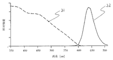
図2は本実施例1にて使用した赤色系発光蛍光体の励起と発光のスペクトル分布を示し、図3は緑色系発光蛍光体の励起と発光のスペクトル分布を示し、そして図4は青色系発光蛍光体の励起と発光のスペクトル分布を示している。すなわち、これらの図に示されたグラフにおいて、横軸は光の波長(nm)を表し、縦軸は光の相対強度を表している。また、グラフ中の曲線31、33、および35は蛍光体の励起スペクトル分布を表し、曲線32、34、および36は蛍光体からの発光スペクトル分布を表している。 2 shows the excitation and emission spectral distribution of the red light emitting phosphor used in Example 1, FIG. 3 shows the excitation and emission spectral distribution of the green light emitting phosphor, and FIG. 4 shows the blue light emission phosphor. The spectral distribution of excitation and emission of the luminescent phosphor is shown. That is, in the graphs shown in these drawings, the horizontal axis represents the wavelength (nm) of light, and the vertical axis represents the relative intensity of light. Further, curves 31, 33, and 35 in the graph represent the excitation spectrum distribution of the phosphor, and curves 32, 34, and 36 represent the emission spectrum distribution from the phosphor.
図2、図3および図4から明らかなように、本実施例1における各蛍光体はピーク波長410nmの1次光によって非常に効率よく赤色、緑色、または青色を発光することがわかる。 As is apparent from FIGS. 2, 3 and 4, each phosphor in Example 1 emits red, green, or blue very efficiently by the primary light having a peak wavelength of 410 nm.
さらに、赤色系発光蛍光体は、緑色系発光蛍光体および青色系発光蛍光体から発せられた緑色光(波長520nm付近)および青色光(波長450nm付近)をも吸収して、赤色を発光し得ることがわかる。 Further, the red light-emitting phosphor can absorb green light (wavelength near 520 nm) and blue light (wavelength near 450 nm) emitted from the green light-emitting phosphor and blue light-emitting phosphor and emit red light. I understand that.
しかしながら、1次光によって励起された蛍光体から2次光として発せられた緑色光(波長520nm付近)および青色光(波長450nm付近)によって赤色系発光蛍光体を励起するのは、全体としての波長変換効率の低下につながるので得策ではない。 However, the red light-emitting phosphor is excited by the green light (wavelength near 520 nm) and the blue light (wavelength near 450 nm) emitted from the phosphor excited by the primary light as a whole. This is not a good idea because it leads to a decrease in conversion efficiency.
すなわち、輝度の高い発光装置を得るためには、本実施例1におけるように赤色系発光蛍光体層13、緑色系発光蛍光体層14、および青色系発光蛍光体層15の順に積層することが重要となる。ただし、緑色系発光蛍光体は青色光によって励起されて発光することがないので、緑色系発光蛍光体と青色系発光蛍光体とを混合して1層の発光層としてもよい。
That is, in order to obtain a light emitting device with high luminance, the red light emitting
本実施例1では、赤色系発光蛍光体、緑色系発光蛍光体、および青色系発光蛍光体の各々をバインダ樹脂(シリコーン系またはエポキシ系)中に混練し、図1に示すデバイスパッケージのカップ16内に赤色発光層13、緑色発光層14、青色発光層15の順に注入して硬化させて蛍光体層構造12を形成した。
In Example 1, each of the red light emitting phosphor, the green light emitting phosphor, and the blue light emitting phosphor is kneaded in a binder resin (silicone or epoxy), and the
なお、蛍光体混練樹脂の注入時にその混練樹脂が表面張力によりカップ16の内壁面を這い上がるのを防止して各発光層の厚さが一定となるように、カップ内壁面には段差(テラス)16aが設けられている。また、カップ内壁は段差16aを境界として上段において下段よりも傾斜が急峻となるように形成されていることが好ましい。このことによって、下段の蛍光体層からの光に関して、段差16aによる影が上段の蛍光体層において少なくされ得る。
In order to prevent the kneaded resin from scooping up the inner wall surface of the
他方、比較例1として、実施例1と全く同種の蛍光体を用いて、青色系発光蛍光体:緑色系発光蛍光体:赤色系発光蛍光体=2.0:1.5:1.0の重量比率で混合した単層の発光層が波長変換部として形成された。 On the other hand, as Comparative Example 1, using the same type of phosphor as in Example 1, blue light-emitting phosphor: green light-emitting phosphor: red light-emitting phosphor = 2.0: 1.5: 1.0 A single-layer light emitting layer mixed at a weight ratio was formed as the wavelength conversion part.
表1において、本実施例1と比較例1の発光装置における白色発光の評価結果が示されている。 In Table 1, evaluation results of white light emission in the light emitting devices of Example 1 and Comparative Example 1 are shown.

表1から明らかなように、本実施例1の発光装置は比較例1に比べて同じ発光色を有しているが、その明るさが飛躍的に向上していることがわかる。 As can be seen from Table 1, the light emitting device of Example 1 has the same emission color as that of Comparative Example 1, but the brightness is dramatically improved.
ここで、Tcは発光装置の発光色の相関色温度を表し、duvは発光色度点の黒体輻射軌跡からの偏差(U*V*W*色度図(CIE1964均等色空間)上における発光色の色度点から黒体輻射軌跡に降ろした垂線の長さ)を表す。duvが0.01以下であれば通常のタングステンフィラメント電球などと同様に、着色のない色と感じられるとされている。また、7000Kの黒体輻射温度では、太陽の色温度に近いことから自然な白色が得られる。 Here, Tc represents the correlated color temperature of the light emission color of the light emitting device, and duv represents the light emission on the deviation (U * V * W * chromaticity diagram (CIE1964 uniform color space) from the black body radiation locus of the light emission chromaticity point. Represents the length of the perpendicular drawn from the chromaticity point of the color to the blackbody radiation locus). If duv is 0.01 or less, it is considered that the color is not colored like a normal tungsten filament bulb. Further, at a black body radiation temperature of 7000 K, a natural white color is obtained because it is close to the color temperature of the sun.
本実施例1および比較例1において、発光素子からの1次光のピーク波長は410nmであって蛍光体の励起のためには効果の高い波長域であるが、視感効率が低いので外部に漏れ出ても発光装置としての明るさには寄与しない。したがって、その1次光のみを反射する特性を有する光学膜(たとえば、多層干渉膜)をコートしたシート12aを蛍光体層構造12の最外面上に貼付することが好ましい。このシート12aによって反射された1次光が再度蛍光体層の励起に寄与し、発光装置全体としてより明るく発光させることができる。
In Example 1 and Comparative Example 1, the peak wavelength of the primary light from the light emitting element is 410 nm, which is a wavelength region that is highly effective for exciting the phosphor. Even if it leaks, it does not contribute to the brightness of the light emitting device. Therefore, it is preferable that a sheet 12 a coated with an optical film (for example, a multilayer interference film) having a characteristic of reflecting only the primary light is stuck on the outermost surface of the
(実施例2)
本発明の実施例2においては、発光素子として、460nmにピ−ク波長を有する窒化ガリウム(GaN)系発光ダイオ−ドが用いられた。
(Example 2)
In Example 2 of the present invention, a gallium nitride (GaN) light emitting diode having a peak wavelength at 460 nm was used as the light emitting element.
波長変換部には、(Sr0.75Ba0.24Eu0.01)2SiO4なる組成で表される緑色系発光蛍光体と(Ca0.985Eu0.015)AlSiN3なる組成で表される赤色系発光蛍光体が用いられた。図2から、赤色系発光蛍光体は緑色系発光蛍光体から発せられた緑色光(波長550nm付近)を吸収し、赤色を発光し得ることがわかる。 For the wavelength conversion unit, a green light emitting phosphor represented by a composition of (Sr 0.75 Ba 0.24 Eu 0.01 ) 2 SiO 4 and a red light emitting phosphor represented by a composition of (Ca 0.985 Eu 0.015 ) AlSiN 3 are used. It was. From FIG. 2, it can be seen that the red light emitting phosphor can absorb green light (wavelength around 550 nm) emitted from the green light emitting phosphor and emit red light.
これらの発光ダイオードと蛍光体を利用して、実施例1と同様な方法にて、本実施例2の発光装置が作成された。また、比較例2として、本実施例2と全く同種の蛍光体を混合した単層の発光層からなる波長変換部を有する発光装置が形成された。 Using these light emitting diodes and phosphors, the light emitting device of Example 2 was produced in the same manner as in Example 1. Further, as Comparative Example 2, a light emitting device having a wavelength conversion unit made of a single light emitting layer in which the same type of phosphor as in Example 2 was mixed was formed.
本実施例2と比較例2による発光装置の特性が評価され、その結果が表2に示されている。 The characteristics of the light emitting devices according to Example 2 and Comparative Example 2 were evaluated, and the results are shown in Table 2.
表2から明らかなように、本実施例2の発光装置は比較例2に比べて同じ発光色を有しているが、その明るさが飛躍的に向上していることがわかる。 As is clear from Table 2, the light emitting device of Example 2 has the same emission color as that of Comparative Example 2, but it can be seen that the brightness is dramatically improved.
(実施例3〜8および比較例3〜8)
用いられる発光素子の発光ピーク波長と蛍光体の種類が変更されたことを除いて、実施例1および比較例1と同様な方法にて、実施例3〜8および比較例3〜8の発光装置がそれぞれ作成され、それらの特性を評価した結果が表3に示されている。
(Examples 3-8 and Comparative Examples 3-8)
The light emitting devices of Examples 3 to 8 and Comparative Examples 3 to 8 were produced in the same manner as in Example 1 and Comparative Example 1, except that the emission peak wavelength of the light emitting element used and the type of phosphor were changed. Table 3 shows the results of evaluating these characteristics.
表3から明らかなように、本発明の実施例3〜8による発光装置は、それぞれ比較例3〜8に比べて、その明るさが飛躍的に向上していることがわかる。 As can be seen from Table 3, the brightness of the light emitting devices according to Examples 3 to 8 of the present invention is significantly improved as compared with Comparative Examples 3 to 8, respectively.
(実施例9)
図1は、本発明の実施例9による白色発光装置に関しても参照することができる。本実施例9の白色発光装置10は、1次光を発する発光素子11と、1次光の少なくとも一部を吸収してその1次光の波長よりも長い波長を有する2次光を発する波長変換部12とを備えている。発光素子11としては、410nmにピ−ク波長を有する窒化ガリウム(GaN)系発光ダイオ−ドが使用された。
Example 9
FIG. 1 can also refer to the white light emitting device according to the ninth embodiment of the present invention. The white
波長変換部12においては、(Ca0.98Eu0.02)AlSiN3の組成で表される赤色系発光蛍光体を含む赤色発光樹脂層13と、(Ba0.85Eu0.15)(Mg0.80Mn0.20)Al10O17の組成で表される緑色系発光蛍光体を含む緑色発光樹脂層14と、(Ba0.80Eu0.20)MgAl10O17の組成で表される青色系発光蛍光体を含む青色発光樹脂層15とが順次積層されており、それらの3種類の蛍光体は1:1:1になるように含められた。
In the
図5は、本実施例9の白色発光装置の発光スペクトル分布を示すグラフである。すなわち、このグラフの横軸は発光波長(nm)を表し、縦軸は光の放射強度(a.u.:任意単位)を表している。このグラフにおいて、2次光として緑色光(ピーク波長520nm付近)を発する蛍光体からの光は、Mnからの発光を反映してそのスペクトル幅が狭くなっていることがわかる。 FIG. 5 is a graph showing the emission spectrum distribution of the white light emitting device of Example 9. That is, the horizontal axis of this graph represents the emission wavelength (nm), and the vertical axis represents the light emission intensity (au: arbitrary unit). In this graph, it can be seen that the spectrum width of the light from the phosphor emitting green light (peak wavelength near 520 nm) as the secondary light is narrow reflecting the light emission from Mn.
本実施例9の白色発光装置について、明るさおよび色再現性(NTSC比)が評価された。この色再現性の測定に使用した青色、緑色、および赤色のカラーフィルタの分光特性が、図6のグラフに示されている。このグラフにおいて、横軸は光の波長(nm)を表し、縦軸は透過光量(任意単位)を表している。また、グラフ中の曲線37は青色フィルタの特性を表し、曲線38は緑色フィルタの曲線を表し、そして曲線39は赤色フィルタの特性を表している。
For the white light emitting device of Example 9, the brightness and color reproducibility (NTSC ratio) were evaluated. The spectral characteristics of the blue, green, and red color filters used for the color reproducibility measurement are shown in the graph of FIG. In this graph, the horizontal axis represents the wavelength (nm) of light, and the vertical axis represents the amount of transmitted light (arbitrary unit). A
他方、本実施例9との比較のために、比較例9としての発光装置も作製された。この比較例9においては、(Ba0.80Eu0.20)MgAl10O17の組成で表される青色系発光蛍光体と(Sr0.92Ba0.05Ca0.01Eu0.02)2SiO4の組成で表される黄色系発光蛍光体とが1.5:1.0の重量比率で混合された単層の樹脂層を波長変換部に用いたことのみにおいて実施例9と異なっていた。 On the other hand, for comparison with Example 9, a light emitting device as Comparative Example 9 was also produced. In Comparative Example 9, a blue light emitting phosphor represented by a composition of (Ba 0.80 Eu 0.20 ) MgAl 10 O 17 and a yellow system represented by a composition of (Sr 0.92 Ba 0.05 Ca 0.01 Eu 0.02 ) 2 SiO 4. It was different from Example 9 only in that a single-layer resin layer mixed with a light emitting phosphor at a weight ratio of 1.5: 1.0 was used for the wavelength conversion section.
表4では、本実施例9と比較例9とによる発光装置における白色発光の評価結果が示されている。 Table 4 shows evaluation results of white light emission in the light emitting devices according to Example 9 and Comparative Example 9.
表4から明らかなように、本実施例9の発光装置は、比較例9の発光装置に比べて、明るさだけでなくて色再現性(NTSC比)も飛躍的に向上していることがわかる。 As is clear from Table 4, the light emitting device of Example 9 has dramatically improved not only brightness but also color reproducibility (NTSC ratio) compared to the light emitting device of Comparative Example 9. Recognize.
なお、表4中で黒体輻射温度が6600Kであって太陽の温度に近いことは、自然な白色が得られることを意味する。 In Table 4, when the black body radiation temperature is 6600 K and is close to the temperature of the sun, it means that a natural white color is obtained.
参考のために、図8のxy色度図において、黒体輻射温度とxy色度図座標との関係を示す。この色度図において、複数の丸印はスペクトルの軌跡を表し、複数の三角印は黒体輻射の軌跡を表している。 For reference, the relationship between black body radiation temperature and xy chromaticity diagram coordinates in the xy chromaticity diagram of FIG. 8 is shown. In this chromaticity diagram, a plurality of circles represent the locus of the spectrum, and a plurality of triangles represent the locus of the black body radiation.
図1を参照し得る本実施例9の発光装置は、より詳細には以下のように作製されている。すなわち、GaN系発光素子11は、一対のリードフレーム(金属薄板)17、18のうちの片方18上に搭載され、一対のワイヤ19によってそれらのリードフレーム17、18へ電気的に接続されている。
The light-emitting device of Example 9 that can refer to FIG. 1 is manufactured in more detail as follows. That is, the GaN-based light emitting element 11 is mounted on one of the pair of lead frames (metal thin plates) 17 and 18 and is electrically connected to the lead frames 17 and 18 by a pair of
発光素子11の周囲には、可視光に対して反射率の高い白色の樹脂によってすり鉢状のカップ16を形成している。すり鉢状の壁面の内側には段差16a、16bを設け、蛍光体を含む樹脂の液面が止まるようにしている。その結果、蛍光体を含む樹脂層13、14、15の各々が、ほぼ所定の厚さになる。
A mortar-shaped
発光素子11は、2次光が赤色の蛍光体を充填した樹脂層13、2次光が緑色の蛍光体を充填した樹脂層14、および2次光が青色の蛍光体を充填した樹脂層15で順次モールドされている。一種の蛍光体を充填した樹脂層でモールドした後に、それを仮硬化してから次の樹脂層を充填することによって、隣接する樹脂層が混ざることを防ぎながら生産効率の低下を防止することができる。
The light-emitting element 11 includes a
なお、カップ16の内壁面は白色樹脂材料のままでもよいが、発光装置の発光効率をさらに高めるために、銀、アルミニウムなどの可視光に対して反射率の高い金属をメッキしておくことがより好ましい。
The inner wall surface of the
図7の模式的な断面図においては、本実施例9による他の形態の発光装置の製造過程が示されている。 In the schematic cross-sectional view of FIG. 7, the manufacturing process of the light emitting device of another form according to the ninth embodiment is shown.
図7(A)において、GaN系発光素子11は硬質の配線基板21上に搭載され、ワイヤ22によってその配線基板21へ電気的に接続される。そして、図7(B)に示されているように、発光素子11は、2次光が赤色の蛍光体を充填した樹脂層、2次光が緑色の蛍光体を充填した樹脂層、および2次光が青色の蛍光体を充填した樹脂層で順次モールドされて、それらの樹脂層を含む樹脂ドーム23によって覆われる。
In FIG. 7A, the GaN-based light emitting element 11 is mounted on a
なお、樹脂ドーム23は、チクソ性の高い樹脂を用いることによって、金型などを用いなくても形成することができる。しかし、樹脂ドーム23に含まれる複数の樹脂層のそれぞれの厚さを正確に設定したい場合は、図7(C)に示されているような金型を用いてもよい。
The
図7(C)においては、赤色発光の蛍光体を含む赤色発光樹脂層23aで発光素子11を覆い、その樹脂層23aは仮硬化してからプレス金型25によって押圧される。こうすることによって、図7(D)に示されているように、発光素子11の頂面からの厚さtを所定の値に設定することができる。同様にして、緑色発光の蛍光体を含む緑色発光樹脂層23bおよび青色発光の蛍光体を含む青色発光樹脂層23cをプレス金型25を用いながら形成することによって、図7(E)に示されているように、厚さ制御された3層の樹脂層23a、23b、23cで覆われた発光素子11を含む白色発光装置が得られる。この場合でも、一種の樹脂層で発光素子11覆って、その樹脂層を仮硬化してから次の樹脂層で覆うことによって、隣接する樹脂層が混ざることを防ぎながら生産効率の低下を防止することができる。
In FIG. 7C, the light emitting element 11 is covered with a red light emitting resin layer 23 a containing a red light emitting phosphor, and the resin layer 23 a is temporarily cured and then pressed by a
(実施例10)
本発明の実施例10においては、発光素子として、390nmのピ−ク波長を有する窒化ガリウム(GaN)系発光ダイオ−ドが用いられた。そして、波長変換部には、(Ca0.985Eu0.015)AlSiN3の組成で表される赤色系発光蛍光体を含む樹脂層と、(Ba0.70Sr0.10Eu0.20)(Mg0.75Mn0.25)Al10O17の組成で表される緑色系発光蛍光体を含む樹脂層と、(Ba0.80Eu0.20)MgAl10O17の組成で表される青色系発光蛍光体を含む樹脂層とが用いられた。
(Example 10)
In Example 10 of the present invention, a gallium nitride (GaN) light emitting diode having a peak wavelength of 390 nm was used as the light emitting element. The wavelength conversion unit includes a resin layer containing a red light emitting phosphor represented by the composition of (Ca 0.985 Eu 0.015 ) AlSiN 3 , and (Ba 0.70 Sr 0.10 Eu 0.20 ) (Mg 0.75 Mn 0.25 ) Al 10 O. A resin layer containing a green light emitting phosphor represented by a composition of 17 and a resin layer containing a blue light emitting phosphor represented by a composition of (Ba 0.80 Eu 0.20 ) MgAl 10 O 17 were used.
他方、本実施例10との比較のための比較例10においては、(Ba0.80Eu0.20)MgAl10O17の組成で表される青色系発光蛍光体と(Y0.52Gd0.35Ce0.13)3Al5O12の組成で表される黄色系発光蛍光体との混合物を含む単層の樹脂層が用いられたことのみにおいて実施例10と異なっていた。 On the other hand, in Comparative Example 10 for comparison with Example 10, the blue light-emitting phosphor represented by the composition of (Ba 0.80 Eu 0.20 ) MgAl 10 O 17 and (Y 0.52 Gd 0.35 Ce 0.13 ) 3 Al It was different from Example 10 only in that a single resin layer containing a mixture with a yellow light emitting phosphor represented by a composition of 5 O 12 was used.
本実施例10および比較例10においても、実施例9の場合と同様に、図1に示されているような形態の発光装置が作製され、それらの発光素子の特性が評価された。それらの評価結果が表5に示されている。 In Example 10 and Comparative Example 10 as well, in the same manner as in Example 9, light-emitting devices having the form shown in FIG. 1 were produced, and the characteristics of these light-emitting elements were evaluated. The evaluation results are shown in Table 5.
表5から明らかなように、本実施例10の発光装置も、比較例10の発光装置に比べて、明るさだけでなくて色再現性(NTSC比)も飛躍的に向上していることがわかる。 As can be seen from Table 5, the light emitting device of Example 10 also has significantly improved not only brightness but also color reproducibility (NTSC ratio) compared to the light emitting device of Comparative Example 10. Recognize.
(実施例11〜15)
実施例9および比較例9に類似して、本発明の実施例11〜15およびそれらと比較される比較例11〜15による発光装置を作製し、それらの発光装置の特性を評価した結果が表6に示されている。ただし、実施例11〜15および比較例11〜15においては、図1に示されているような形態の発光装置が作製されたが、表6に示されているように、用いられた発光素子の発光ピーク波長と蛍光体の組成とが種々に変更された。
(Examples 11 to 15)
Similar to Example 9 and Comparative Example 9, light-emitting devices according to Examples 11 to 15 of the present invention and Comparative Examples 11 to 15 compared with them were manufactured, and the results of evaluating the characteristics of these light-emitting devices are shown in Table 1. 6. However, in Examples 11 to 15 and Comparative Examples 11 to 15, the light emitting device having the form as shown in FIG. 1 was produced. As shown in Table 6, the light emitting element used was used. The emission peak wavelength and the phosphor composition were variously changed.
表6から明らかなように、本発明による蛍光体を含む実施例11〜15の発光装置は、青色発光の発光素子とその青色により励起されて黄色発光を示す2価のユ−ロピウムで付活された(Sr,Ba,Ca)2SiO4蛍光体またはそれと3価のセリウムで付活された(Y,Gd)3(Al,Ga)5O12蛍光体との組合せを含む比較例11〜15の発光装置に比べて、明るさだけでなくで色再現性(NTSC比)も飛躍的に向上していることがわかる。 As is apparent from Table 6, the light emitting devices of Examples 11 to 15 including the phosphor according to the present invention are activated by a blue light emitting element and divalent europium which is excited by the blue light and emits yellow light. Comparative Examples 11 to 11 including a combination of a (Sr, Ba, Ca) 2 SiO 4 phosphor or a (Y, Gd) 3 (Al, Ga) 5 O 12 phosphor activated with trivalent cerium Compared to the 15 light emitting devices, not only the brightness but also the color reproducibility (NTSC ratio) is dramatically improved.
本発明では、発光素子から発する1次光のピ−ク波長が380nmから450nmの範囲にあればよく、390nmから420nmの範囲内のピ−ク波長を有する発光素子が本発明の発光装置により適している。 In the present invention, the peak wavelength of the primary light emitted from the light emitting element only needs to be in the range of 380 nm to 450 nm, and the light emitting element having a peak wavelength in the range of 390 nm to 420 nm is more suitable for the light emitting device of the present invention. ing.
なお、色再現性(NTSC比)を飛躍的に向上させるためには、緑色系発光蛍光体(またはそれに含まれる緑色系発光成分)の発光スペクトルの半値幅を狭くすることが望まれる。これを達成するためには、本発明におけるように、2価のマンガン(Mn)による発光が適しており、また緑色系発光蛍光体の母体としてはアルミン酸塩(Aluminate)が適している。 In order to drastically improve the color reproducibility (NTSC ratio), it is desired to reduce the half-value width of the emission spectrum of the green light emitting phosphor (or the green light emitting component contained therein). In order to achieve this, light emission by divalent manganese (Mn) is suitable as in the present invention, and aluminate is suitable as the base of the green light-emitting phosphor.
上述の実施例では、発光素子に近い方から、2次光の波長の長い蛍光体を含む樹脂層の順に積層することを特徴としている。しかし、本発明における三色の蛍光体を混合して含む単層の樹脂層を用いた場合には、明るさが著しく低下するものの、色再現性(NTSC比)には影響がない。したがって、色再現性(NTSC比)の向上のみを追求する場合には、三色の蛍光体を混合して含む単層の樹脂層を使用してもよい。 The above-described embodiment is characterized in that the resin layers including phosphors having a long wavelength of secondary light are laminated in order from the side closer to the light emitting element. However, when a single-layer resin layer containing a mixture of three color phosphors in the present invention is used, the brightness is remarkably reduced, but the color reproducibility (NTSC ratio) is not affected. Therefore, in the case where only improvement in color reproducibility (NTSC ratio) is pursued, a single resin layer containing a mixture of three color phosphors may be used.
また、上述の実施例では、緑色系発光蛍光体を含む樹脂層上に青色系発光蛍光体を含む樹脂層を積層している。しかし、本発明における緑色系発光蛍光体においては、波長450nm前後の1次青色光の励起による2次発光強度が弱い。したがって、緑色系発光蛍光体と青色系発光蛍光体とを混合して単層の樹脂層に含めても、白色発光としての明るさの低下は少なく、本発明における作用および効果は変わらない。 In the above-described embodiment, the resin layer including the blue light-emitting phosphor is laminated on the resin layer including the green light-emitting phosphor. However, the green light-emitting phosphor in the present invention has a weak secondary emission intensity due to excitation of primary blue light having a wavelength of around 450 nm. Therefore, even when a green light emitting phosphor and a blue light emitting phosphor are mixed and included in a single resin layer, the brightness as white light emission is hardly reduced, and the function and effect of the present invention are not changed.
(実施例16)
図9において、本発明の実施例16による発光装置の要部が模式的な縦断面図で図解されている。図9の発光装置では、白色樹脂からなりかつ段差を含まない反射面(内周面)を有するすり鉢状のカップ46の底面上に発光素子11が搭載され、その発光素子11は所定の様式で分布させられた蛍光体粒子43、44、45を含む透光性樹脂42で封止されていることにおいて、図1の発光装置と異なっている。
(Example 16)
In FIG. 9, the principal part of the light-emitting device by Example 16 of this invention is illustrated with the typical longitudinal cross-sectional view. In the light-emitting device of FIG. 9, the light-emitting element 11 is mounted on the bottom surface of a mortar-shaped
透光性樹脂42としてはエポキシ樹脂、シリコーン樹脂などが用いられ得る。透光性樹脂42には赤色系発光蛍光体粒子43、緑色系発光蛍光体粒子44、および青色系発光蛍光体粒子45から選ばれた少なくとも2種以上が含まれ、それらの蛍光体粒子は種類に依存して概略層状に分離して分布させられている。ここで、より短い2次光波長を有する蛍光体粒子が発光素子11から遠い位置に分布させられている。
As the
すなわち、透光性樹脂42は大粒径蛍光粒子43、中粒径蛍光粒子44、および小粒径蛍光粒子45を含み、それらの蛍光粒子が層状に分離している。このような場合、大粒径蛍光粒子から発せられた光は、小粒径蛍光粒子で散乱されて、均一な放射光にされ得る。
That is, the
図9に示されているような発光装置は、以下のようにして作製され得る。すなわち、透光性樹脂42に含まれる蛍光体は上述のように赤色系発光蛍光体粒子43、緑色系発光蛍光体粒子44、および青色系発光蛍光体粒子45から選ばれた少なくとも2種以上であり、各種類の蛍光体粒子は硬化前の液状の透光性樹脂中で、互いに沈降速度が異なるように粒子径が調整される。
The light emitting device as shown in FIG. 9 can be manufactured as follows. That is, the phosphor contained in the
液状樹脂中の蛍光粒子の沈降速度は、蛍光粒子に働く重力と粒子表面に接する液状樹脂による摩擦力の大きさとで決まり、その重力は粒径の三乗に比例し、摩擦力は粒径の自乗に比例するので、粒径の大小が沈降速度に大きく影響する。液状樹脂との摩擦力は、樹脂の種類にあまり依存せず、主に蛍光体粒子の表面状態に依存し、蛍光体の材質や表面処理に依存して異なる。 The sedimentation rate of the fluorescent particles in the liquid resin is determined by the gravity acting on the fluorescent particles and the magnitude of the frictional force due to the liquid resin in contact with the particle surface, and the gravity is proportional to the cube of the particle size, and the frictional force is the particle size. Since it is proportional to the square, the size of the particle size greatly affects the sedimentation rate. The frictional force with the liquid resin does not depend much on the type of the resin, mainly depends on the surface state of the phosphor particles, and varies depending on the phosphor material and surface treatment.
一般に、特殊な表面処理を施していない蛍光体粒子においては、粒径の細かい蛍光体の方が単位質量当たりの表面積が大きくなるので、その沈降速度は粒径の粗い場合に比べて遅くなる(特許文献8の国際公開第02/059982号パンフレット参照)。なお、一次蛍光体粒子が凝集して二次粒子を形成している場合には、一次粒子の粒径ではなく二次粒子の径に依存して沈降速度が決まる。実際の蛍光体粒子は理想的な球形ではないので単純に比較することはできないが、概略的には上述の議論が成立すると考えられる。 In general, in phosphor particles that have not been subjected to special surface treatment, the surface area per unit mass of a phosphor with a smaller particle size is larger, so the sedimentation rate is slower than when the particle size is coarse ( (See International Publication No. 02/059982 pamphlet of Patent Document 8). In the case where the primary phosphor particles are aggregated to form secondary particles, the sedimentation speed is determined depending on the diameter of the secondary particles, not the diameter of the primary particles. Since the actual phosphor particles are not ideal spheres, they cannot be simply compared, but the above discussion is considered to be valid.
上述のように沈降速度差を利用して、液状樹脂中に分散された粒子を粒径に依存させて分離するには、実用的には無機材料の蛍光体粒子で数μmの寸法であることが望まれる。たとえば、特許文献1に開示されているように粒径がボーア半径程度まで小さくされている場合には、分離に要する時間が非常に長くなってしまって実用的ではない。
As described above, in order to separate the particles dispersed in the liquid resin depending on the particle size using the difference in the sedimentation rate, it is practically a size of several μm with phosphor particles of inorganic material. Is desired. For example, as disclosed in
本実施例16では、赤色系、緑色系、および青色系の蛍光体粒子として、たとえばメジアン径がそれぞれ13μm、9.5μm、および6.5μmのものを使用し得る。ここで、メジアン径とは、粒径の分布の中央値を意味する。粒子の大きさを表すパラメータとしては平均粒子直径d50もしばしば用いられるが、どちらで表現しても本発明の作用効果には大きな影響を及ぼすことはない。なお、蛍光体種の明瞭な分離のためには、各蛍光体種における粒径の分布が狭いほど好ましいことは言うまでもない。 In Example 16, red, green, and blue phosphor particles having median diameters of 13 μm, 9.5 μm, and 6.5 μm, respectively, can be used. Here, the median diameter means the median value of the particle size distribution. An average particle diameter d 50 is often used as a parameter representing the size of the particle, but neither of them will significantly affect the operational effects of the present invention. Needless to say, for a clear separation of the phosphor species, the narrower the particle size distribution in each phosphor species, the better.
より具体的には、再度図9を参照して、沈降速度が異なる複数種の蛍光体粒子43、44、45を一緒に液状の透光性樹脂42中に混練して、発光素子11が搭載されたカップ46内に注入する。この後、蛍光体粒子43、44、45を含む透光性樹脂42を所定時間静置する。そうすれば、沈降速度の大きい蛍光体種43は、カップ46底面側で濃度がより高く、カップ底面から離れるにしたがって濃度が低くなるように分布する。逆に、沈降速度の小さい蛍光体種45はカップ底面で濃度が小さくなり、カップ底面から離れるにしたがって濃度が高くなるように分布する。このようにして、沈降速度の大きさに依存して、蛍光体種の濃度分布が形成され得る。
More specifically, referring again to FIG. 9, a plurality of types of
なお、以上の実施例において示された蛍光体を表す化学式および組成比は例示であって、本発明の作用効果を得るためには、前述の「課題を解決するための手段」において示された蛍光体の組成および組成比を満たせばよことに留意されたい。 In addition, the chemical formulas and composition ratios representing the phosphors shown in the above examples are exemplifications, and in order to obtain the effects of the present invention, they are shown in the above-mentioned “Means for Solving Problems”. It should be noted that the phosphor composition and composition ratio should be satisfied.
以上のように、本発明によれば、発光素子からの紫外光または青色光にて高効率に発光する複数種の蛍光体を波長変換部に利用する発光装置であって、発光色の設定が容易でありかつ輝度の高い発光装置を提供することができ、さらには、色再現性(NTSC比)が著しく良好な白色光を放射し得る発光装置を提供することができる。 As described above, according to the present invention, there is provided a light emitting device that uses a plurality of types of phosphors that emit light with high efficiency by ultraviolet light or blue light from a light emitting element in a wavelength conversion unit, and the emission color is set. A light-emitting device that is easy and has high luminance can be provided, and furthermore, a light-emitting device that can emit white light with extremely good color reproducibility (NTSC ratio) can be provided.
10 発光装置、11 発光素子、12 波長変換部、12a 光学膜、13 赤色系発光蛍光体を含む樹脂層、14 緑色系発光蛍光体を含む樹脂層、15 青色系発光蛍光体を含む樹脂層、16 カップ、16a 段差(テラス)、17 アノード端子、18 カソード端子、19 金ワイヤ、21 配線基板、22 ワイヤ、23 蛍光体を含む樹脂ドーム、23a 赤色系発光蛍光体を含む樹脂層、23b 緑色系発光蛍光体を含む樹脂層、23c 青色系発光蛍光体を含む樹脂層、25 プレス金型、31、33、35 励起スペクトル、32、34、36 発光スペクトル、37 青色フィルタ、38 緑色フィルタ、39 赤色フィルタ、41 カップ、42 蛍光体を含む樹脂層、43 赤色系発光蛍光体粒子、44 緑色系発光蛍光体粒子、45 青色系発光蛍光体粒子。
DESCRIPTION OF
Claims (20)
前記1次光の一部を吸収してその1次光の波長以上の波長を有する2次光を発する波長変換部とを含み、
前記波長変換部は互いに異なる光吸収帯域を有する複数種の蛍光体を含み、
前記複数種の蛍光体の少なくとも1種は他の少なくとも1種で発せられた2次光を吸収し得る吸収帯域を有することを特徴とする発光装置。 A light emitting element that emits primary light;
A wavelength converter that absorbs a part of the primary light and emits secondary light having a wavelength equal to or greater than the wavelength of the primary light;
The wavelength conversion unit includes a plurality of types of phosphors having different light absorption bands,
At least one of the plurality of types of phosphors has an absorption band capable of absorbing secondary light emitted from at least one other type.
(M1,Eu)10(PO4)6・Cl2で表される2価のユーロピウム付活ハロ燐酸塩蛍光体、
a(M2,Eu)O・bAl2O3で表される2価のユ−ロピウム付活アルミン酸塩蛍光体、および
a(M2,Euc,Mnd)O・bAl2O3で表される2価のユーロピウムおよびマンガン共付活アルミン酸塩蛍光体から選ばれる少なくとも1種を含み、
ここで、M1はMg、Ca、SrおよびBaから選ばれる少なくとも1種の元素を表し、M2はMg、Ca、Sr、BaおよびZnから選ばれる少なくとも1種の元素を表し、a、b、cおよびdはa>0、b>0、0.1≦a/b≦1.0、0.001≦d/c≦0.2を満足する数を表すことを特徴とする請求項4に記載の発光装置。 The blue light emitting phosphor is
A divalent europium-activated halophosphate phosphor represented by (M1, Eu) 10 (PO 4 ) 6 .Cl 2 ;
a (M2, Eu) O · bAl 2 divalent Yoo represented by 2 O 3 - europium-activated aluminate phosphor, and a (M2, Eu c, Mn d) is represented by O · bAl 2 O 3 Including at least one selected from divalent europium and manganese co-activated aluminate phosphors,
Here, M1 represents at least one element selected from Mg, Ca, Sr and Ba, M2 represents at least one element selected from Mg, Ca, Sr, Ba and Zn, and a, b, c And d represents a number satisfying a> 0, b> 0, 0.1 ≦ a / b ≦ 1.0, and 0.001 ≦ d / c ≦ 0.2. Light-emitting device.
a(M2,Eue,Mnf)O・bAl2O3で表される2価のユーロピウムおよびマンガン共付活アルミン酸塩蛍光体、
2(M11-g,Eug)O・SiO2で表される2価のユーロピウム付活珪酸塩蛍光体、および
MI3(MII1-h,Ceh)2(SiO4)3で表される3価のセリウム付活珪酸塩蛍光体から選ばれる少なくとも1種を含み、
ここで、M2はMg、Ca、Sr、BaおよびZnから選ばれる少なくとも1種の元素を表し、a、b、eおよびfはa>0、b>0、0.1≦a/b≦1.0、0.3≦f/e≦5.0を満足する数を表し、M1はMg、Ca、SrおよびBaから選ばれる少なくとも1種の元素を表し、gは0.005≦g≦0.10を満足する数を表し、MIはMg、Ca、SrおよびBaから選ばれる少なくとも1種の元素を表し、MIIはAl、Ga、In、Sc、Y、La、GdおよびLuから選ばれる少なくとも1種の元素を表し、hは0.01≦h≦0.4を満足する数を表すことを特徴とする請求項4または5に記載の発光装置。 The green light-emitting phosphor is
a (M2, Eu e, Mn f) O · bAl 2 O 3 in the divalent europium and manganese co-activated aluminate phosphor represented by,
2 (M1 1-g, Eu g) 2 divalent europium-activated silicate phosphor represented by O · SiO 2, and MI 3 (MII 1-h, Ce h) is represented by 2 (SiO 4) 3 Including at least one selected from trivalent cerium activated silicate phosphors,
Here, M2 represents at least one element selected from Mg, Ca, Sr, Ba and Zn, and a, b, e and f are a> 0, b> 0, 0.1 ≦ a / b ≦ 1. 0.0, 0.3 ≦ f / e ≦ 5.0, M1 represents at least one element selected from Mg, Ca, Sr and Ba, and g is 0.005 ≦ g ≦ 0. .10, MI represents at least one element selected from Mg, Ca, Sr and Ba, and MII represents at least selected from Al, Ga, In, Sc, Y, La, Gd and Lu. 6. The light emitting device according to claim 4, wherein the light emitting device represents one element, and h represents a number satisfying 0.01 ≦ h ≦ 0.4.
前記1次光の少なくとも一部を吸収してその1次光の波長以上の波長を有する2次光を発する波長変換部とを含み、
前記波長変換部は少なくとも緑色系発光蛍光体と赤色系発光蛍光体とを含み、
前記緑色系発光蛍光体は、a(M2,Eue,Mnf)O・bAl2O3で表される2価のユーロピウムおよびマンガン共付活アルミン酸塩蛍光体を含み、ここで、M2はMg、Ca、Sr、BaおよびZnから選ばれる少なくとも1種の元素を表し、a、b、eおよびfはa>0、b>0、0.1≦a/b≦1.0、および0.3≦f/e≦5.0を満足する数を表すことを特徴とする発光装置。 A light emitting element that emits primary light;
A wavelength converter that absorbs at least part of the primary light and emits secondary light having a wavelength equal to or greater than the wavelength of the primary light;
The wavelength conversion unit includes at least a green light emitting phosphor and a red light emitting phosphor,
The green light-emitting phosphor comprises a (M2, Eu e, Mn f) O · bAl 2 O 3 in the divalent europium and manganese co-activated aluminate phosphor represented, wherein, M2 is Represents at least one element selected from Mg, Ca, Sr, Ba and Zn, wherein a, b, e and f are a> 0, b> 0, 0.1 ≦ a / b ≦ 1.0, and 0 A light-emitting device that represents a number satisfying 3 ≦ f / e ≦ 5.0.
(M1,Eu)10(PO4)6・Cl2で表される2価のユーロピウム付活ハロ燐酸塩蛍光体、
a(M2,Eu)O・bAl2O3で表される2価のユーロピウム付活アルミン酸塩蛍光体、および
a(M2,Euc,Mnd)O・bAl2O3で表される2価のユーロピウムおよびマンガン共付活アルミン酸塩蛍光体から選ばれる少なくとも1種を含み、
ここで、M1はMg、Ca、SrおよびBaから選ばれる少なくとも1種の元素を表し、M2はMg、Ca、Sr、BaおよびZnから選ばれる少なくとも1種の元素を表し、a、b、cおよびdはa>0、b>0、0.1≦a/b≦1.0、および0.001≦d/c≦0.2を満足する数を表すことを特徴とする請求項9に記載の発光装置。 The wavelength conversion unit further includes a blue light emitting phosphor, and the blue light emitting phosphor is:
A divalent europium-activated halophosphate phosphor represented by (M1, Eu) 10 (PO 4 ) 6 .Cl 2 ;
a (M2, Eu) O · bAl 2 O 3 in the divalent europium-activated aluminate phosphor represented, and a (M2, Eu c, Mn d) 2 represented by O · bAl 2 O 3 At least one selected from valent europium and manganese co-activated aluminate phosphors,
Here, M1 represents at least one element selected from Mg, Ca, Sr and Ba, M2 represents at least one element selected from Mg, Ca, Sr, Ba and Zn, and a, b, c And d represents a number satisfying a> 0, b> 0, 0.1 ≦ a / b ≦ 1.0, and 0.001 ≦ d / c ≦ 0.2. The light-emitting device of description.
前記パッケージ内に搭載された前記発光素子を覆うように、第1の蛍光体種が混錬された第1の液状樹脂を注入して硬化させる工程と、
硬化した前記第1液状樹脂および前記反射面の上に、前記第1蛍光体種に比べて短い2次光波長を有する第2の蛍光体種が混錬された第2の液状樹脂を注入して硬化させる工程とを含むことを特徴とする発光装置の製造方法。 Mounting the light emitting element on the bottom surface surrounded by the reflective surface of the inner wall of the package;
Injecting and curing a first liquid resin mixed with a first phosphor species so as to cover the light emitting element mounted in the package;
A second liquid resin mixed with a second phosphor species having a secondary light wavelength shorter than that of the first phosphor species is injected onto the cured first liquid resin and the reflecting surface. And a step of curing the light emitting device.
前記パッケージ内に搭載された前記発光素子を覆うように、粒径のメディアン値が異なる複数種の蛍光体が混練された液状樹脂を注入する工程と、
前記注入された液状樹脂を所定時間静置させて、粒径のメディアン値が大きい蛍光体種ほど前記発光素子近くで濃度が高くなるように沈降させる工程とを含むことを特徴とする発光装置の製造方法。 Mounting the light emitting element on the bottom surface surrounded by the reflective surface of the inner wall of the package;
Injecting a liquid resin in which a plurality of types of phosphors having different particle size median values are kneaded so as to cover the light emitting element mounted in the package;
A step of allowing the injected liquid resin to stand for a predetermined time and allowing the phosphor seed having a larger median value of particle size to settle so as to increase in concentration near the light emitting element. Production method.
Priority Applications (7)
| Application Number | Priority Date | Filing Date | Title |
|---|---|---|---|
| JP2006059689A JP2007049114A (en) | 2005-05-30 | 2006-03-06 | Light emitting device and manufacturing method thereof |
| US11/442,000 US7737621B2 (en) | 2005-05-30 | 2006-05-26 | Light emitting device provided with a wavelength conversion unit incorporating plural kinds of phosphors |
| CN2009101417389A CN101562227B (en) | 2005-05-30 | 2006-05-30 | Light emitting device and method of manufacturing the same |
| US12/774,495 US8729788B2 (en) | 2005-05-30 | 2010-05-05 | Light emitting device provided with a wavelength conversion unit incorporating plural kinds of phosphors |
| US14/254,619 US9281456B2 (en) | 2005-05-30 | 2014-04-16 | Light emitting device and fabricating method thereof |
| US15/008,020 US9722149B2 (en) | 2005-05-30 | 2016-01-27 | Light emitting device and fabricating method thereof |
| US15/630,286 US10008644B2 (en) | 2005-05-30 | 2017-06-22 | Light emitting device and fabricating method thereof |
Applications Claiming Priority (3)
| Application Number | Priority Date | Filing Date | Title |
|---|---|---|---|
| JP2005157056 | 2005-05-30 | ||
| JP2005202851 | 2005-07-12 | ||
| JP2006059689A JP2007049114A (en) | 2005-05-30 | 2006-03-06 | Light emitting device and manufacturing method thereof |
Related Child Applications (1)
| Application Number | Title | Priority Date | Filing Date |
|---|---|---|---|
| JP2011095929A Division JP2011151419A (en) | 2005-05-30 | 2011-04-22 | Light emitting device and manufacturing method thereof |
Publications (1)
| Publication Number | Publication Date |
|---|---|
| JP2007049114A true JP2007049114A (en) | 2007-02-22 |
Family
ID=37082545
Family Applications (1)
| Application Number | Title | Priority Date | Filing Date |
|---|---|---|---|
| JP2006059689A Pending JP2007049114A (en) | 2005-05-30 | 2006-03-06 | Light emitting device and manufacturing method thereof |
Country Status (2)
| Country | Link |
|---|---|
| US (5) | US7737621B2 (en) |
| JP (1) | JP2007049114A (en) |
Cited By (50)
| Publication number | Priority date | Publication date | Assignee | Title |
|---|---|---|---|---|
| JP2007191680A (en) * | 2005-09-01 | 2007-08-02 | Sharp Corp | Light emitting device |
| JP2008244468A (en) * | 2007-02-28 | 2008-10-09 | Toshiba Lighting & Technology Corp | Light emitting device |
| JP2008288409A (en) * | 2007-05-18 | 2008-11-27 | Toshiba Corp | Light emitting device and manufacturing method thereof |
| JP2008311245A (en) * | 2007-06-12 | 2008-12-25 | Nichia Corp | Light emitting device |
| JP2009019163A (en) * | 2007-07-13 | 2009-01-29 | Sharp Corp | Phosphor particle assembly for light emitting device, light emitting device, and backlight device for liquid crystal display |
| WO2009028370A1 (en) * | 2007-08-30 | 2009-03-05 | Toppan Printing Co., Ltd. | Liquid crystal display device and color filter used for the same |
| JP2009516774A (en) * | 2005-11-22 | 2009-04-23 | ルミネイション リミテッド ライアビリティ カンパニー | Charge compensated nitride phosphors for use in lighting applications |
| JP2009540551A (en) * | 2006-06-07 | 2009-11-19 | オスラム オプト セミコンダクターズ ゲゼルシャフト ミット ベシュレンクテル ハフツング | Method for disposing a powder layer on a substrate and layer structure having at least one powder layer on a substrate |
| JP2010093237A (en) * | 2008-10-13 | 2010-04-22 | Advanced Optoelectronic Technology Inc | System and method for manufacturing light emitting diode back light unit provided with high color reproducibility |
| JP2010198805A (en) * | 2009-02-23 | 2010-09-09 | Casio Computer Co Ltd | Light source device and projector |
| JP2010287680A (en) * | 2009-06-10 | 2010-12-24 | Mitsubishi Chemicals Corp | Light emitting device |
| JP2011071333A (en) * | 2009-09-25 | 2011-04-07 | Mitsubishi Chemicals Corp | Color rendering property-improving method for white light-emitting device, and white light-emitting device |
| JP2011119402A (en) * | 2009-12-02 | 2011-06-16 | Fuji Electric Fa Components & Systems Co Ltd | Light source unit |
| JP2011519162A (en) * | 2008-04-25 | 2011-06-30 | クリー インコーポレイテッド | Semiconductor light emitting device having separated wavelength converting material and method for forming the same |
| JP2011159970A (en) * | 2010-01-28 | 2011-08-18 | Lg Innotek Co Ltd | Light emitting element package |
| JP2011249368A (en) * | 2010-05-21 | 2011-12-08 | Sharp Corp | Semiconductor light-emitting device |
| JP2011530817A (en) * | 2008-08-11 | 2011-12-22 | オスラム ゲゼルシャフト ミット ベシュレンクテル ハフツング | Conversion type LED |
| WO2012032880A1 (en) * | 2010-09-10 | 2012-03-15 | 株式会社日立製作所 | Wavelength-converting resin composition, sealing material for wavelength-conversion-type solar cell and process for production thereof, and solar cell module and process for production thereof |
| JP2012104531A (en) * | 2010-11-08 | 2012-05-31 | Koito Mfg Co Ltd | Light emitting module |
| JP2012142346A (en) * | 2010-12-28 | 2012-07-26 | Hitachi Ltd | Wavelength conversion type sealing material sheet and solar battery module |
| JP2012195425A (en) * | 2011-03-16 | 2012-10-11 | Toshiba Corp | Semiconductor light-emitting device wafer and method of manufacturing semiconductor light-emitting device |
| JP2012529134A (en) * | 2009-06-05 | 2012-11-15 | オスラム オプト セミコンダクターズ ゲゼルシャフト ミット ベシュレンクテル ハフツング | Optical irradiation apparatus and optical recording apparatus |
| JP2012230968A (en) * | 2011-04-25 | 2012-11-22 | Hitachi Chem Co Ltd | Sealing material sheet and solar battery module |
| EP2541632A2 (en) | 2011-06-28 | 2013-01-02 | Sharp Kabushiki Kaisha | Light emitting device and method for producing the same |
| JP2013046046A (en) * | 2011-08-26 | 2013-03-04 | Mitsubishi Chemicals Corp | Light-emitting device |
| US8415870B2 (en) | 2008-08-28 | 2013-04-09 | Panasonic Corporation | Semiconductor light emitting device and backlight source, backlight source system, display device and electronic device using the same |
| JP2013110356A (en) * | 2011-11-24 | 2013-06-06 | Sharp Corp | Solar cell module and solar light power generation apparatus |
| JP2013118244A (en) * | 2011-12-02 | 2013-06-13 | Citizen Holdings Co Ltd | Semiconductor light-emitting device and lighting apparatus using the same |
| JP2013201434A (en) * | 2008-02-25 | 2013-10-03 | Toshiba Corp | Light-emitting device, display device, and lighting device |
| JP2013539223A (en) * | 2010-09-23 | 2013-10-17 | オスラム ゲーエムベーハー | Optoelectronic semiconductor devices |
| KR101360624B1 (en) * | 2007-08-31 | 2014-02-07 | 엘지이노텍 주식회사 | Lighting emitting diode package and fabrication method thereof |
| US8663498B2 (en) | 2006-11-24 | 2014-03-04 | Sharp Kabushiki Kaisha | Phosphor, method of producing the same, and light emitting apparatus |
| KR101478124B1 (en) * | 2012-12-12 | 2015-01-02 | 경북대학교 산학협력단 | Led package and menufacturing method of the same |
| JP2015015418A (en) * | 2013-07-08 | 2015-01-22 | シャープ株式会社 | Semiconductor light emitting device |
| JP2015195397A (en) * | 2015-07-13 | 2015-11-05 | 日立化成株式会社 | Solar battery module |
| KR101575366B1 (en) * | 2010-02-02 | 2015-12-07 | 엘지이노텍 주식회사 | Light emitting device package |
| US9281456B2 (en) | 2005-05-30 | 2016-03-08 | Sharp Kabushiki Kaisha | Light emitting device and fabricating method thereof |
| JP2016086168A (en) * | 2014-10-24 | 2016-05-19 | シチズン電子株式会社 | Light emitting device and manufacturing method thereof |
| KR20160104681A (en) | 2014-01-28 | 2016-09-05 | 샤프 가부시키가이샤 | Light-emitting diode driver and illumination device |
| US9614130B2 (en) | 2013-11-08 | 2017-04-04 | Sharp Kabushiki Kaisha | Light emitting device and illumination device |
| KR101748696B1 (en) | 2010-09-20 | 2017-06-19 | 엘지디스플레이 주식회사 | Discharging system of fluorescence material and silicon and mixing method of fluorescence material and silicon using thereof |
| WO2017169773A1 (en) * | 2016-03-31 | 2017-10-05 | シャープ株式会社 | Eye-safe light source and method for manufacturing same |
| JP2017533549A (en) * | 2014-10-01 | 2017-11-09 | コーニンクレッカ フィリップス エヌ ヴェKoninklijke Philips N.V. | Light source with adjustable emission spectrum |
| JP2018053128A (en) * | 2016-09-29 | 2018-04-05 | 日亜化学工業株式会社 | Light-emitting device |
| US10018776B2 (en) | 2013-04-15 | 2018-07-10 | Sharp Kabushiki Kaisha | Illumination device, illumination equipment, and display device |
| JP2018113411A (en) * | 2017-01-13 | 2018-07-19 | 日亜化学工業株式会社 | Light emitting device |
| US10270015B1 (en) | 2017-01-13 | 2019-04-23 | Nichia Corporation | Light-emitting device |
| JP2019165257A (en) * | 2017-01-13 | 2019-09-26 | 日亜化学工業株式会社 | Light-emitting device |
| US10461225B2 (en) | 2015-03-09 | 2019-10-29 | Toyoda Gosei Co., Ltd. | Method of manufacturing light-emitting device including sealing materials with phosphor particles |
| US10741732B2 (en) | 2018-01-31 | 2020-08-11 | Nichia Corporation | Light emitting device and light source |
Families Citing this family (106)
| Publication number | Priority date | Publication date | Assignee | Title |
|---|---|---|---|---|
| US7858408B2 (en) * | 2004-11-15 | 2010-12-28 | Koninklijke Philips Electronics N.V. | LED with phosphor tile and overmolded phosphor in lens |
| JP4794235B2 (en) * | 2005-08-02 | 2011-10-19 | シャープ株式会社 | Light emitting device |
| US20070052342A1 (en) * | 2005-09-01 | 2007-03-08 | Sharp Kabushiki Kaisha | Light-emitting device |
| US8441179B2 (en) * | 2006-01-20 | 2013-05-14 | Cree, Inc. | Lighting devices having remote lumiphors that are excited by lumiphor-converted semiconductor excitation sources |
| WO2008045927A2 (en) * | 2006-10-12 | 2008-04-17 | Cree Led Lighting Solutions, Inc. | Lighting device and method of making same |
| JP2010525512A (en) * | 2007-04-17 | 2010-07-22 | コーニンクレッカ フィリップス エレクトロニクス エヌ ヴィ | Lighting system |
| JP4920497B2 (en) * | 2007-05-29 | 2012-04-18 | 株式会社東芝 | Optical semiconductor device |
| US20100181580A1 (en) * | 2007-07-19 | 2010-07-22 | Masatsugu Masuda | Light emitting apparatus |
| US7863635B2 (en) * | 2007-08-07 | 2011-01-04 | Cree, Inc. | Semiconductor light emitting devices with applied wavelength conversion materials |
| CN101809768B (en) * | 2007-08-31 | 2012-04-25 | Lg伊诺特有限公司 | Light emitting device package |
| JP2011501466A (en) * | 2007-10-26 | 2011-01-06 | クリー エル イー ディー ライティング ソリューションズ インコーポレイテッド | Lighting device having one or more light emitters and method of making the same |
| CN101911318A (en) * | 2007-12-28 | 2010-12-08 | 3M创新有限公司 | Down-conversion light source emitting uniform wavelength |
| US10008637B2 (en) | 2011-12-06 | 2018-06-26 | Cree, Inc. | Light emitter devices and methods with reduced dimensions and improved light output |
| KR101429704B1 (en) * | 2008-01-31 | 2014-08-12 | 삼성디스플레이 주식회사 | Wavelength transforming member, Light assembly having the same, and liquid crystal display |
| KR101476421B1 (en) | 2008-03-31 | 2014-12-26 | 서울반도체 주식회사 | Backlight unit |
| KR100992778B1 (en) | 2008-05-23 | 2010-11-05 | 엘지이노텍 주식회사 | Light emitting device package and method for manufacturing the same |
| JP5239043B2 (en) * | 2008-07-18 | 2013-07-17 | シャープ株式会社 | Light emitting device and method for manufacturing light emitting device |
| JP5284006B2 (en) * | 2008-08-25 | 2013-09-11 | シチズン電子株式会社 | Light emitting device |
| TW201011942A (en) * | 2008-09-11 | 2010-03-16 | Advanced Optoelectronic Tech | Method and system for configuring high CRI LED |
| DE102008050643B4 (en) * | 2008-10-07 | 2022-11-03 | OSRAM Opto Semiconductors Gesellschaft mit beschränkter Haftung | bulbs |
| DE102008054175A1 (en) * | 2008-10-31 | 2010-05-06 | Osram Gesellschaft mit beschränkter Haftung | Low-pressure discharge lamp |
| US8704244B2 (en) * | 2009-02-05 | 2014-04-22 | Ccs, Inc. | LED light emitting device |
| US8921876B2 (en) | 2009-06-02 | 2014-12-30 | Cree, Inc. | Lighting devices with discrete lumiphor-bearing regions within or on a surface of remote elements |
| DE102009037730A1 (en) | 2009-08-17 | 2011-02-24 | Osram Gesellschaft mit beschränkter Haftung | Conversion LED with high color rendering |
| JP2011171557A (en) * | 2010-02-19 | 2011-09-01 | Toshiba Corp | Light emitting device, method of manufacturing the same, and light emitting device manufacturing apparatus |
| US8716038B2 (en) * | 2010-03-02 | 2014-05-06 | Micron Technology, Inc. | Microelectronic workpiece processing systems and associated methods of color correction |
| US9275979B2 (en) | 2010-03-03 | 2016-03-01 | Cree, Inc. | Enhanced color rendering index emitter through phosphor separation |
| JP5635832B2 (en) * | 2010-08-05 | 2014-12-03 | スタンレー電気株式会社 | Semiconductor light emitting device |
| CN102376860A (en) | 2010-08-05 | 2012-03-14 | 夏普株式会社 | Light emitting apparatus and method for manufacturing thereof |
| TWI432668B (en) * | 2010-10-11 | 2014-04-01 | Optromax Corp | White light illumination device and method for generating white light |
| US11251164B2 (en) | 2011-02-16 | 2022-02-15 | Creeled, Inc. | Multi-layer conversion material for down conversion in solid state lighting |
| US8742654B2 (en) * | 2011-02-25 | 2014-06-03 | Cree, Inc. | Solid state light emitting devices including nonhomogeneous luminophoric particle size layers |
| US8957438B2 (en) | 2011-04-07 | 2015-02-17 | Cree, Inc. | Methods of fabricating light emitting devices including multiple sequenced luminophoric layers |
| EP4258819A3 (en) * | 2011-04-22 | 2024-01-24 | Seoul Semiconductor Co., Ltd. | White light equipment |
| CN102563543B (en) | 2011-05-09 | 2015-01-07 | 深圳市绎立锐光科技开发有限公司 | Method and light source for generating high-brightness homogeneous light based on optical wavelength conversion |
| JP5105132B1 (en) * | 2011-06-02 | 2012-12-19 | 三菱化学株式会社 | Semiconductor light emitting device, semiconductor light emitting system, and lighting fixture |
| US10490712B2 (en) | 2011-07-21 | 2019-11-26 | Cree, Inc. | Light emitter device packages, components, and methods for improved chemical resistance and related methods |
| US10686107B2 (en) | 2011-07-21 | 2020-06-16 | Cree, Inc. | Light emitter devices and components with improved chemical resistance and related methods |
| US10211380B2 (en) | 2011-07-21 | 2019-02-19 | Cree, Inc. | Light emitting devices and components having improved chemical resistance and related methods |
| EP2739704B1 (en) * | 2011-08-04 | 2015-10-14 | Koninklijke Philips N.V. | Light converter and lighting unit comprising such light converter |
| TWI505515B (en) * | 2011-08-19 | 2015-10-21 | Epistar Corp | Light emitting device and method of manufacturing same |
| TWI448806B (en) | 2011-09-22 | 2014-08-11 | Delta Electronics Inc | Phosphor device and illumination system and projection equipment with the same |
| US10688527B2 (en) | 2011-09-22 | 2020-06-23 | Delta Electronics, Inc. | Phosphor device comprising plural phosphor agents for converting waveband light into plural color lights with different wavelength peaks |
| US10310363B2 (en) | 2011-09-22 | 2019-06-04 | Delta Electronics, Inc. | Phosphor device with spectrum of converted light comprising at least a color light |
| EP2772953B1 (en) * | 2011-10-24 | 2022-01-26 | Seoul Semiconductor Co., Ltd. | White light source and white light source system using white light source |
| US9496466B2 (en) | 2011-12-06 | 2016-11-15 | Cree, Inc. | Light emitter devices and methods, utilizing light emitting diodes (LEDs), for improved light extraction |
| CN102544328A (en) * | 2012-01-20 | 2012-07-04 | 江苏索尔光电科技有限公司 | LED encapsulation piece |
| KR101957700B1 (en) * | 2012-02-01 | 2019-03-14 | 삼성전자주식회사 | Ligt Emitting Device |
| US9343441B2 (en) * | 2012-02-13 | 2016-05-17 | Cree, Inc. | Light emitter devices having improved light output and related methods |
| US8946747B2 (en) | 2012-02-13 | 2015-02-03 | Cree, Inc. | Lighting device including multiple encapsulant material layers |
| US9240530B2 (en) | 2012-02-13 | 2016-01-19 | Cree, Inc. | Light emitter devices having improved chemical and physical resistance and related methods |
| US8957580B2 (en) | 2012-02-13 | 2015-02-17 | Cree, Inc. | Lighting device including multiple wavelength conversion material layers |
| US9269876B2 (en) * | 2012-03-06 | 2016-02-23 | Soraa, Inc. | Light emitting diodes with low refractive index material layers to reduce light guiding effects |
| US10145026B2 (en) | 2012-06-04 | 2018-12-04 | Slt Technologies, Inc. | Process for large-scale ammonothermal manufacturing of semipolar gallium nitride boules |
| JP6107001B2 (en) * | 2012-09-04 | 2017-04-05 | ソニー株式会社 | Scintillator and radiation detection apparatus |
| KR102019499B1 (en) * | 2012-11-05 | 2019-09-06 | 엘지이노텍 주식회사 | Light emitting device and lighting systme having thereof |
| US9761763B2 (en) | 2012-12-21 | 2017-09-12 | Soraa, Inc. | Dense-luminescent-materials-coated violet LEDs |
| JP6102273B2 (en) * | 2013-01-18 | 2017-03-29 | 日亜化学工業株式会社 | Light emitting device and manufacturing method thereof |
| US9142732B2 (en) * | 2013-03-04 | 2015-09-22 | Osram Sylvania Inc. | LED lamp with quantum dots layer |
| CN105190163A (en) * | 2013-04-24 | 2015-12-23 | 日立麦克赛尔株式会社 | Light source device and vehicle light fixture |
| DE102013214235A1 (en) | 2013-07-19 | 2015-01-22 | Osram Gmbh | Lighting device with semiconductor light sources and circumferential dam |
| TWI596805B (en) * | 2013-07-24 | 2017-08-21 | 晶元光電股份有限公司 | Light-emitting element and manufacturing method thereof |
| DE102013226630A1 (en) * | 2013-12-19 | 2015-06-25 | Osram Gmbh | Conversion element, component and method for producing a component |
| DE102014102848B4 (en) * | 2013-12-19 | 2025-01-02 | Osram Gmbh | Conversion element, method for producing a conversion element, optoelectronic component comprising a conversion element |
| JP6358457B2 (en) * | 2014-01-20 | 2018-07-18 | パナソニックIpマネジメント株式会社 | Light emitting device, illumination light source, and illumination device |
| TWI528601B (en) * | 2014-04-30 | 2016-04-01 | 新世紀光電股份有限公司 | Packaging method and package structure |
| US9660151B2 (en) * | 2014-05-21 | 2017-05-23 | Nichia Corporation | Method for manufacturing light emitting device |
| JP6303805B2 (en) * | 2014-05-21 | 2018-04-04 | 日亜化学工業株式会社 | Light emitting device and manufacturing method thereof |
| JP6428089B2 (en) | 2014-09-24 | 2018-11-28 | 日亜化学工業株式会社 | Light emitting device |
| US11997768B2 (en) * | 2014-09-28 | 2024-05-28 | Zhejiang Super Lighting Electric Appliance Co., Ltd | LED filament and LED light bulb |
| JP6462713B2 (en) | 2014-10-28 | 2019-01-30 | 株式会社東芝 | White light source system |
| DE102015107580A1 (en) * | 2015-05-13 | 2016-11-17 | Osram Opto Semiconductors Gmbh | Radiation-emitting optoelectronic component |
| JP2017017059A (en) * | 2015-06-26 | 2017-01-19 | パナソニックIpマネジメント株式会社 | Illumination light source and illumination device |
| US9735323B2 (en) * | 2015-06-30 | 2017-08-15 | Nichia Corporation | Light emitting device having a triple phosphor fluorescent member |
| JP6680868B2 (en) | 2015-08-17 | 2020-04-15 | インフィニット アースロスコピー インコーポレーテッド, リミテッド | light source |
| JP6644081B2 (en) * | 2015-11-04 | 2020-02-12 | シャープ株式会社 | Light-emitting device, lighting device, and method for manufacturing light-emitting body included in light-emitting device |
| CN106816520A (en) * | 2015-11-30 | 2017-06-09 | 隆达电子股份有限公司 | Wavelength conversion materials and their applications |
| CN107017325B (en) | 2015-11-30 | 2020-06-23 | 隆达电子股份有限公司 | Quantum dot composite material and its manufacturing method and application |
| TWI618946B (en) * | 2015-12-22 | 2018-03-21 | Delta Electronics, Inc. | Phosphor device and manufacturing method thereof |
| KR20170075897A (en) | 2015-12-23 | 2017-07-04 | 삼성전자주식회사 | Light emitting diode package |
| CN107304984B (en) * | 2016-04-22 | 2020-06-09 | 松下电器产业株式会社 | Wavelength conversion member and projector |
| JP6493348B2 (en) * | 2016-09-30 | 2019-04-03 | 日亜化学工業株式会社 | Light emitting device |
| US10388838B2 (en) * | 2016-10-19 | 2019-08-20 | Genesis Photonics Inc. | Light-emitting device and manufacturing method thereof |
| KR102674066B1 (en) | 2016-11-11 | 2024-06-13 | 삼성전자주식회사 | Light emitting device package |
| KR102831200B1 (en) * | 2017-02-02 | 2025-07-10 | 서울반도체 주식회사 | Light emitting diode package |
| ES2955917T3 (en) | 2017-02-15 | 2023-12-11 | Lazurite Holdings Llc | Wireless medical imaging system comprising head unit and light cable comprising integrated light source |
| US10340426B2 (en) * | 2017-07-06 | 2019-07-02 | Epistar Corporation | Phosphor and illumination device utilizing the same |
| JP7092474B2 (en) * | 2017-08-21 | 2022-06-28 | シチズン電子株式会社 | Light emitting device |
| CN111052410B (en) * | 2017-09-05 | 2023-06-13 | 夏普株式会社 | Light emitting device |
| JP6940764B2 (en) | 2017-09-28 | 2021-09-29 | 日亜化学工業株式会社 | Light emitting device |
| JP6665872B2 (en) | 2018-01-15 | 2020-03-13 | 日亜化学工業株式会社 | Light emitting device and method of manufacturing light emitting device |
| US10804442B2 (en) | 2018-01-29 | 2020-10-13 | Nichia Corporation | Light emitting device |
| EP3758077A4 (en) * | 2018-02-23 | 2021-11-24 | Kyocera Corporation | LIGHT EMITTING DEVICE AND LIGHTING DEVICE |
| JP6912728B2 (en) * | 2018-03-06 | 2021-08-04 | 日亜化学工業株式会社 | Light emitting device and light source device |
| JP7095937B2 (en) * | 2018-03-09 | 2022-07-05 | ミネベアミツミ株式会社 | Manufacturing method of fluorescent sheet |
| WO2019240150A1 (en) * | 2018-06-12 | 2019-12-19 | 国立研究開発法人産業技術総合研究所 | Light-emitting device |
| KR102530363B1 (en) * | 2018-08-31 | 2023-05-09 | 루미레즈 엘엘씨 | Phosphor conversion LEDs with high color quality |
| US11732187B2 (en) * | 2018-10-25 | 2023-08-22 | Nichia Corporation | Chlorosilicate fluorescent material, method for producing the same, and light emitting device |
| WO2020214810A1 (en) * | 2019-04-16 | 2020-10-22 | Infinite Arthroscopy, Inc. Limited | Light source converter |
| USD938584S1 (en) | 2020-03-30 | 2021-12-14 | Lazurite Holdings Llc | Hand piece |
| CN112447896A (en) * | 2020-05-26 | 2021-03-05 | 开发晶照明(厦门)有限公司 | Photoelectric device and manufacturing method thereof |
| CN111628066A (en) * | 2020-06-04 | 2020-09-04 | 江西鸿利光电有限公司 | A kind of process method of improving LED luminous brightness |
| USD972176S1 (en) | 2020-08-06 | 2022-12-06 | Lazurite Holdings Llc | Light source |
| US20220254962A1 (en) * | 2021-02-11 | 2022-08-11 | Creeled, Inc. | Optical arrangements in cover structures for light emitting diode packages and related methods |
| JP7627578B2 (en) * | 2021-02-22 | 2025-02-06 | スタンレー電気株式会社 | Light emitting device and method for manufacturing the same |
| US20240154076A1 (en) * | 2022-11-08 | 2024-05-09 | Creeled, Inc. | Lumiphoric material structures for light-emitting diode packages and related methods |
Citations (7)
| Publication number | Priority date | Publication date | Assignee | Title |
|---|---|---|---|---|
| JPH1187770A (en) * | 1997-09-01 | 1999-03-30 | Toshiba Electron Eng Corp | Illumination device, reading device, projection device, purification device, and display device |
| JP2000031531A (en) * | 1998-07-14 | 2000-01-28 | Toshiba Electronic Engineering Corp | Light emitting device |
| JP2004179644A (en) * | 2002-11-12 | 2004-06-24 | Nichia Chem Ind Ltd | Phosphor laminate structure and light source using the same |
| JP2005093896A (en) * | 2003-09-19 | 2005-04-07 | Stanley Electric Co Ltd | Semiconductor light emitting device |
| WO2005044947A2 (en) * | 2003-10-29 | 2005-05-19 | Gelcore Llc | Garnet phosphor materials having enhanced spectral characteristics |
| JP2005277127A (en) * | 2004-03-25 | 2005-10-06 | Stanley Electric Co Ltd | Light emitting device |
| JP2006063233A (en) * | 2004-08-27 | 2006-03-09 | Dowa Mining Co Ltd | Phosphor mixture and light emitting device |
Family Cites Families (109)
| Publication number | Priority date | Publication date | Assignee | Title |
|---|---|---|---|---|
| US3707641A (en) * | 1970-12-22 | 1972-12-26 | Westinghouse Electric Corp | Discharge device which utilizes a mixture of two fluorescent materials |
| NL160869C (en) | 1972-11-03 | Philips Nv | LUMINESCENT SCREEN, AS WELL AS DISCHARGE LAMP AND KATHODE BEAM TUBE, FITTED WITH SUCH SCREEN. | |
| US4390637A (en) | 1980-09-10 | 1983-06-28 | Nippon Electric Glass Company, Limited | X-Ray absorbing glass for a color cathode ray tube having a controlled chromaticity value and a selective light absorption |
| JP2790673B2 (en) | 1989-09-20 | 1998-08-27 | 化成オプトニクス株式会社 | Aluminate phosphor |
| EP0686997A3 (en) | 1994-06-06 | 1996-06-26 | Matsushita Electric Industrial Co Ltd | Discharge lamp and lighting device for general lighting |
| TW353678B (en) | 1994-08-17 | 1999-03-01 | Mitsubishi Chem Corp | Aluminate phosphor |
| WO1997050132A1 (en) | 1996-06-26 | 1997-12-31 | Siemens Aktiengesellschaft | Light-emitting semiconductor component with luminescence conversion element |
| TW383508B (en) | 1996-07-29 | 2000-03-01 | Nichia Kagaku Kogyo Kk | Light emitting device and display |
| JP2927279B2 (en) | 1996-07-29 | 1999-07-28 | 日亜化学工業株式会社 | Light emitting diode |
| JPH10228868A (en) | 1997-02-13 | 1998-08-25 | Ind Technol Res Inst | Method for improving luminous efficiency of plasma display |
| JP3095366B2 (en) | 1997-04-07 | 2000-10-03 | 北川精機株式会社 | Press control method and press device |
| US6340824B1 (en) | 1997-09-01 | 2002-01-22 | Kabushiki Kaisha Toshiba | Semiconductor light emitting device including a fluorescent material |
| JPH11140437A (en) * | 1997-11-06 | 1999-05-25 | Matsushita Electric Ind Co Ltd | Method for producing divalent europium-activated phosphor |
| JP3486345B2 (en) | 1998-07-14 | 2004-01-13 | 東芝電子エンジニアリング株式会社 | Semiconductor light emitting device |
| JP2000109826A (en) | 1998-10-05 | 2000-04-18 | Kasei Optonix Co Ltd | Alkaline earth aluminate phosphor and fluorescent lamp |
| US6429583B1 (en) | 1998-11-30 | 2002-08-06 | General Electric Company | Light emitting device with ba2mgsi2o7:eu2+, ba2sio4:eu2+, or (srxcay ba1-x-y)(a1zga1-z)2sr:eu2+phosphors |
| JP3081842B1 (en) | 1999-07-13 | 2000-08-28 | ファインセラミックス技術研究組合 | α-sialon particles |
| US6686691B1 (en) * | 1999-09-27 | 2004-02-03 | Lumileds Lighting, U.S., Llc | Tri-color, white light LED lamps |
| TWI272299B (en) * | 1999-10-06 | 2007-02-01 | Sumitomo Chemical Co | A process for producing aluminate-based phosphor |
| JP2001127346A (en) | 1999-10-22 | 2001-05-11 | Stanley Electric Co Ltd | Light emitting diode |
| JP2001172623A (en) | 1999-12-20 | 2001-06-26 | Toshiba Corp | Phosphor and fluorescent lamp using the same |
| TWI285217B (en) * | 2000-04-06 | 2007-08-11 | Sumitomo Chemical Co | Vacuum ultraviolet ray-excited light-emitting phosphor |
| JP3515737B2 (en) | 2000-06-22 | 2004-04-05 | 松下電器産業株式会社 | Phosphor and fluorescent lamp using the same |
| JP2002003836A (en) | 2000-06-22 | 2002-01-09 | Matsushita Electric Ind Co Ltd | Phosphor and fluorescent lamp using the same |
| TW574343B (en) * | 2000-06-27 | 2004-02-01 | Sumitomo Chemical Co | Method of producing aluminate fluorescent substance, a fluorescent substance and a device containing a fluorescent substance |
| DE10036940A1 (en) * | 2000-07-28 | 2002-02-07 | Patent Treuhand Ges Fuer Elektrische Gluehlampen Mbh | Luminescence conversion LED |
| US6635363B1 (en) | 2000-08-21 | 2003-10-21 | General Electric Company | Phosphor coating with self-adjusting distance from LED chip |
| JP4077170B2 (en) | 2000-09-21 | 2008-04-16 | シャープ株式会社 | Semiconductor light emitting device |
| MY131962A (en) | 2001-01-24 | 2007-09-28 | Nichia Corp | Light emitting diode, optical semiconductor device, epoxy resin composition suited for optical semiconductor device, and method for manufacturing the same |
| JP3447274B2 (en) | 2001-02-22 | 2003-09-16 | 化成オプトニクス株式会社 | Method for producing aluminate phosphor |
| JP2002275462A (en) | 2001-03-21 | 2002-09-25 | Nemoto & Co Ltd | Fluorescent substance for electric lamp and method of producing the same |
| JP4101468B2 (en) * | 2001-04-09 | 2008-06-18 | 豊田合成株式会社 | Method for manufacturing light emitting device |
| US7091656B2 (en) * | 2001-04-20 | 2006-08-15 | Nichia Corporation | Light emitting device |
| JP3668770B2 (en) | 2001-06-07 | 2005-07-06 | 独立行政法人物質・材料研究機構 | Oxynitride phosphor activated with rare earth elements |
| US6632379B2 (en) | 2001-06-07 | 2003-10-14 | National Institute For Materials Science | Oxynitride phosphor activated by a rare earth element, and sialon type phosphor |
| DE10133352A1 (en) | 2001-07-16 | 2003-02-06 | Patent Treuhand Ges Fuer Elektrische Gluehlampen Mbh | Lighting unit with at least one LED as a light source |
| JP2003121838A (en) | 2001-08-06 | 2003-04-23 | Toray Ind Inc | Liquid crystal display device |
| US7189340B2 (en) | 2004-02-12 | 2007-03-13 | Mitsubishi Chemical Corporation | Phosphor, light emitting device using phosphor, and display and lighting system using light emitting device |
| JP4032682B2 (en) | 2001-08-28 | 2008-01-16 | 三菱化学株式会社 | Phosphor |
| DE10146719A1 (en) | 2001-09-20 | 2003-04-17 | Patent Treuhand Ges Fuer Elektrische Gluehlampen Mbh | Lighting unit with at least one LED as a light source |
| US7294956B2 (en) * | 2001-10-01 | 2007-11-13 | Matsushita Electric Industrial Co., Ltd. | Semiconductor light emitting element and light emitting device using this |
| JP3985486B2 (en) | 2001-10-01 | 2007-10-03 | 松下電器産業株式会社 | Semiconductor light emitting element and light emitting device using the same |
| JP3946541B2 (en) | 2002-02-25 | 2007-07-18 | 三菱電線工業株式会社 | LIGHT EMITTING DEVICE, LIGHTING DEVICE USING THE SAME, AND METHOD FOR MANUFACTURING AND DESIGNING THE LIGHT EMITTING DEVICE |
| WO2003080764A1 (en) | 2002-03-22 | 2003-10-02 | Nichia Corporation | Nitride phosphor and method for preparation thereof, and light emitting device |
| JP4214768B2 (en) | 2002-11-29 | 2009-01-28 | 日亜化学工業株式会社 | Nitride phosphor and light emitting device using the same |
| JP2003321675A (en) | 2002-04-26 | 2003-11-14 | Nichia Chem Ind Ltd | Nitride phosphor and method for producing the same |
| CA2427559A1 (en) | 2002-05-15 | 2003-11-15 | Sumitomo Electric Industries, Ltd. | White color light emitting device |
| JP3707446B2 (en) | 2002-05-28 | 2005-10-19 | 住友電気工業株式会社 | White light emitting device |
| JP3655267B2 (en) | 2002-07-17 | 2005-06-02 | 株式会社東芝 | Semiconductor light emitting device |
| JP4197109B2 (en) | 2002-08-06 | 2008-12-17 | 静雄 藤田 | Lighting device |
| JP4222059B2 (en) | 2002-09-24 | 2009-02-12 | 日亜化学工業株式会社 | Light emitting device |
| US6717353B1 (en) * | 2002-10-14 | 2004-04-06 | Lumileds Lighting U.S., Llc | Phosphor converted light emitting device |
| JP2004210921A (en) | 2002-12-27 | 2004-07-29 | Nichia Chem Ind Ltd | Oxynitride phosphor, method of manufacturing the same, and light emitting device using the same |
| JP3775377B2 (en) | 2002-11-06 | 2006-05-17 | 日亜化学工業株式会社 | Manganese-activated aluminate phosphor, method for producing the same, and vacuum ultraviolet-excited light emitting device |
| JP4207537B2 (en) | 2002-11-08 | 2009-01-14 | 日亜化学工業株式会社 | Phosphor and light emitting device |
| JP2004161871A (en) | 2002-11-12 | 2004-06-10 | Nichia Chem Ind Ltd | Sintered phosphor layer |
| JP4072632B2 (en) | 2002-11-29 | 2008-04-09 | 豊田合成株式会社 | Light emitting device and light emitting method |
| JP4124684B2 (en) | 2003-03-25 | 2008-07-23 | セイコーインスツル株式会社 | Transflective liquid crystal display device |
| JP4274843B2 (en) * | 2003-04-21 | 2009-06-10 | シャープ株式会社 | LED device and mobile phone device, digital camera and LCD display device using the same |
| DE10324832A1 (en) * | 2003-06-02 | 2004-12-23 | Patent-Treuhand-Gesellschaft für elektrische Glühlampen mbH | Discharge lamp with fluorescent |
| US7026755B2 (en) | 2003-08-07 | 2006-04-11 | General Electric Company | Deep red phosphor for general illumination applications |
| US7285913B2 (en) | 2003-08-29 | 2007-10-23 | Matsushita Electric Industrial Co., Ltd. | Plasma display device having blue phosphor layers with alkaline earth metal aluminate containing molybdenum or tungsten |
| JP2005091480A (en) | 2003-09-12 | 2005-04-07 | Nitto Denko Corp | Method for producing anisotropic film |
| US7723740B2 (en) | 2003-09-18 | 2010-05-25 | Nichia Corporation | Light emitting device |
| JP2005109085A (en) | 2003-09-30 | 2005-04-21 | Okaya Electric Ind Co Ltd | Light emitting diode |
| US7488432B2 (en) * | 2003-10-28 | 2009-02-10 | Nichia Corporation | Fluorescent material and light-emitting device |
| JP3837588B2 (en) | 2003-11-26 | 2006-10-25 | 独立行政法人物質・材料研究機構 | Phosphors and light emitting devices using phosphors |
| KR100540848B1 (en) * | 2004-01-02 | 2006-01-11 | 주식회사 메디아나전자 | White light emitting diode device composed of double mold and manufacturing method |
| US7250715B2 (en) | 2004-02-23 | 2007-07-31 | Philips Lumileds Lighting Company, Llc | Wavelength converted semiconductor light emitting devices |
| TWI262609B (en) | 2004-02-27 | 2006-09-21 | Dowa Mining Co | Phosphor and manufacturing method thereof, and light source, LED using said phosphor |
| JP4511849B2 (en) | 2004-02-27 | 2010-07-28 | Dowaエレクトロニクス株式会社 | Phosphor and its manufacturing method, light source, and LED |
| JP2005244075A (en) | 2004-02-27 | 2005-09-08 | Matsushita Electric Works Ltd | Light emitting device |
| JP3921545B2 (en) | 2004-03-12 | 2007-05-30 | 独立行政法人物質・材料研究機構 | Phosphor and production method thereof |
| JP2005298805A (en) | 2004-03-16 | 2005-10-27 | Mitsubishi Chemicals Corp | Light emitting device and lighting device |
| JP2005272486A (en) | 2004-03-22 | 2005-10-06 | Fujikura Ltd | Powder phosphor, alpha sialon phosphor manufacturing method and light emitting device |
| TWI286393B (en) | 2004-03-24 | 2007-09-01 | Toshiba Lighting & Technology | Lighting apparatus |
| US7391060B2 (en) | 2004-04-27 | 2008-06-24 | Matsushita Electric Industrial Co., Ltd. | Phosphor composition and method for producing the same, and light-emitting device using the same |
| JP4128564B2 (en) | 2004-04-27 | 2008-07-30 | 松下電器産業株式会社 | Light emitting device |
| US7077978B2 (en) * | 2004-05-14 | 2006-07-18 | General Electric Company | Phosphors containing oxides of alkaline-earth and group-IIIB metals and white-light sources incorporating same |
| JP4565141B2 (en) | 2004-06-30 | 2010-10-20 | 独立行政法人物質・材料研究機構 | Phosphors and light emitting devices |
| US8417215B2 (en) | 2004-07-28 | 2013-04-09 | Koninklijke Philips Electronics N.V. | Method for positioning of wireless medical devices with short-range radio frequency technology |
| US7453195B2 (en) * | 2004-08-02 | 2008-11-18 | Lumination Llc | White lamps with enhanced color contrast |
| JP4729281B2 (en) * | 2004-09-13 | 2011-07-20 | 株式会社フジクラ | Light emitting diode and light emitting diode manufacturing method |
| JP4674348B2 (en) | 2004-09-22 | 2011-04-20 | 独立行政法人物質・材料研究機構 | Phosphor, method for producing the same, and light emitting device |
| US7265488B2 (en) * | 2004-09-30 | 2007-09-04 | Avago Technologies General Ip Pte. Ltd | Light source with wavelength converting material |
| JP2006114637A (en) * | 2004-10-13 | 2006-04-27 | Toshiba Corp | Semiconductor light emitting device |
| KR101267284B1 (en) | 2004-10-15 | 2013-08-07 | 미쓰비시 가가꾸 가부시키가이샤 | Fluorescent material, fluorescent device using the same, and image display device and lighting equipment |
| EP1672755B1 (en) | 2004-12-17 | 2015-09-23 | Nichia Corporation | Light emitting device |
| JP4720177B2 (en) | 2004-12-17 | 2011-07-13 | 日亜化学工業株式会社 | Light emitting device |
| WO2006068141A1 (en) | 2004-12-24 | 2006-06-29 | Kabushiki Kaisha Toshiba | White led, backlight using same and liquid crystal display |
| CN102585810A (en) | 2005-02-28 | 2012-07-18 | 电气化学工业株式会社 | Fluorescent substance and process for producing the same, and luminescent element using the same |
| JP4104013B2 (en) | 2005-03-18 | 2008-06-18 | 株式会社フジクラ | LIGHT EMITTING DEVICE AND LIGHTING DEVICE |
| JP4692059B2 (en) | 2005-04-25 | 2011-06-01 | パナソニック電工株式会社 | Method for manufacturing light emitting device |
| KR100682874B1 (en) | 2005-05-02 | 2007-02-15 | 삼성전기주식회사 | White LED |
| JP2006332269A (en) | 2005-05-25 | 2006-12-07 | Toyoda Gosei Co Ltd | Light emitting device |
| JP2007049114A (en) | 2005-05-30 | 2007-02-22 | Sharp Corp | Light emitting device and manufacturing method thereof |
| JP4817728B2 (en) | 2005-06-29 | 2011-11-16 | 株式会社東芝 | Ultrasonic diagnostic equipment |
| JP4794235B2 (en) * | 2005-08-02 | 2011-10-19 | シャープ株式会社 | Light emitting device |
| US20070052342A1 (en) | 2005-09-01 | 2007-03-08 | Sharp Kabushiki Kaisha | Light-emitting device |
| JP4832995B2 (en) | 2005-09-01 | 2011-12-07 | シャープ株式会社 | Light emitting device |
| JP4769132B2 (en) | 2005-11-30 | 2011-09-07 | シャープ株式会社 | Light emitting device |
| EP1985683B1 (en) | 2006-02-02 | 2013-08-28 | Mitsubishi Chemical Corporation | Complex oxynitride phosphor, light-emitting device using same, image display, illuminating device, phosphor-containing composition and complex oxynitride |
| WO2008001799A1 (en) | 2006-06-27 | 2008-01-03 | Mitsubishi Chemical Corporation | Illuminating device |
| JP5367218B2 (en) | 2006-11-24 | 2013-12-11 | シャープ株式会社 | Method for manufacturing phosphor and method for manufacturing light emitting device |
| JP2009019163A (en) | 2007-07-13 | 2009-01-29 | Sharp Corp | Phosphor particle assembly for light emitting device, light emitting device, and backlight device for liquid crystal display |
| JP2009094199A (en) | 2007-10-05 | 2009-04-30 | Sharp Corp | Light emitting device, surface light source, display device, and manufacturing method thereof |
| JP5239941B2 (en) | 2009-02-26 | 2013-07-17 | 豊田合成株式会社 | Method for manufacturing light emitting device |
| WO2011013188A1 (en) | 2009-07-27 | 2011-02-03 | 株式会社 東芝 | Light-emitting device |
| JP4740379B1 (en) | 2010-02-25 | 2011-08-03 | 電気化学工業株式会社 | β-type sialon phosphor, its use and method for producing β-type sialon phosphor |
-
2006
- 2006-03-06 JP JP2006059689A patent/JP2007049114A/en active Pending
- 2006-05-26 US US11/442,000 patent/US7737621B2/en active Active
-
2010
- 2010-05-05 US US12/774,495 patent/US8729788B2/en active Active
-
2014
- 2014-04-16 US US14/254,619 patent/US9281456B2/en not_active Expired - Fee Related
-
2016
- 2016-01-27 US US15/008,020 patent/US9722149B2/en active Active
-
2017
- 2017-06-22 US US15/630,286 patent/US10008644B2/en active Active
Patent Citations (7)
| Publication number | Priority date | Publication date | Assignee | Title |
|---|---|---|---|---|
| JPH1187770A (en) * | 1997-09-01 | 1999-03-30 | Toshiba Electron Eng Corp | Illumination device, reading device, projection device, purification device, and display device |
| JP2000031531A (en) * | 1998-07-14 | 2000-01-28 | Toshiba Electronic Engineering Corp | Light emitting device |
| JP2004179644A (en) * | 2002-11-12 | 2004-06-24 | Nichia Chem Ind Ltd | Phosphor laminate structure and light source using the same |
| JP2005093896A (en) * | 2003-09-19 | 2005-04-07 | Stanley Electric Co Ltd | Semiconductor light emitting device |
| WO2005044947A2 (en) * | 2003-10-29 | 2005-05-19 | Gelcore Llc | Garnet phosphor materials having enhanced spectral characteristics |
| JP2005277127A (en) * | 2004-03-25 | 2005-10-06 | Stanley Electric Co Ltd | Light emitting device |
| JP2006063233A (en) * | 2004-08-27 | 2006-03-09 | Dowa Mining Co Ltd | Phosphor mixture and light emitting device |
Non-Patent Citations (2)
| Title |
|---|
| 上田恭太 他: "赤色窒化物蛍光体(CaAlSiN3:Eu2+)の発光特性", 応用物理学会学術講演会講演予稿集, vol. 65, no. 3, JPN6011005537, 1 September 2004 (2004-09-01), JP, pages 1283, ISSN: 0001850618 * |
| 上田恭太 他: "赤色窒化物蛍光体(CaAlSiN3:Eu2+)の発光特性", 応用物理学会学術講演会講演予稿集, vol. 65, no. 3, JPN6011042676, 1 September 2004 (2004-09-01), JP, pages 1283, ISSN: 0001992467 * |
Cited By (69)
| Publication number | Priority date | Publication date | Assignee | Title |
|---|---|---|---|---|
| US10008644B2 (en) | 2005-05-30 | 2018-06-26 | Sharp Kabushiki Kaisha | Light emitting device and fabricating method thereof |
| US9281456B2 (en) | 2005-05-30 | 2016-03-08 | Sharp Kabushiki Kaisha | Light emitting device and fabricating method thereof |
| US9722149B2 (en) | 2005-05-30 | 2017-08-01 | Sharp Kabushiki Kaisha | Light emitting device and fabricating method thereof |
| JP2007191680A (en) * | 2005-09-01 | 2007-08-02 | Sharp Corp | Light emitting device |
| JP2009516774A (en) * | 2005-11-22 | 2009-04-23 | ルミネイション リミテッド ライアビリティ カンパニー | Charge compensated nitride phosphors for use in lighting applications |
| JP2009540551A (en) * | 2006-06-07 | 2009-11-19 | オスラム オプト セミコンダクターズ ゲゼルシャフト ミット ベシュレンクテル ハフツング | Method for disposing a powder layer on a substrate and layer structure having at least one powder layer on a substrate |
| US8202747B2 (en) | 2006-06-07 | 2012-06-19 | Osram Opto Semiconductors Gmbh | Method for arranging a powder layer on a substrate and layer structure with at least one powder layer on a substrate |
| US10259997B2 (en) | 2006-11-24 | 2019-04-16 | Ge Phosphors Technology, Llc | Phosphor, method of producing the same, and light emitting apparatus |
| US8663498B2 (en) | 2006-11-24 | 2014-03-04 | Sharp Kabushiki Kaisha | Phosphor, method of producing the same, and light emitting apparatus |
| US9884990B2 (en) | 2006-11-24 | 2018-02-06 | Ge Phosphors Technology, Llc | Phosphor, method of producing the same, and light emitting apparatus |
| US9624427B2 (en) | 2006-11-24 | 2017-04-18 | Ge Phosphors Technology, Llc | Phosphor, method of producing the same, and light emitting apparatus |
| JP2008244468A (en) * | 2007-02-28 | 2008-10-09 | Toshiba Lighting & Technology Corp | Light emitting device |
| US8419497B2 (en) | 2007-05-18 | 2013-04-16 | Kabushiki Kaisha Toshiba | Light emitting device and method of manufacturing the same |
| JP2008288409A (en) * | 2007-05-18 | 2008-11-27 | Toshiba Corp | Light emitting device and manufacturing method thereof |
| JP2008311245A (en) * | 2007-06-12 | 2008-12-25 | Nichia Corp | Light emitting device |
| JP2009019163A (en) * | 2007-07-13 | 2009-01-29 | Sharp Corp | Phosphor particle assembly for light emitting device, light emitting device, and backlight device for liquid crystal display |
| US7808012B2 (en) | 2007-07-13 | 2010-10-05 | Sharp Kabushiki Kaisha | Group of phosphor particles for light-emitting device, light-emitting device and backlight for liquid crystal display |
| TWI451161B (en) * | 2007-08-30 | 2014-09-01 | 凸版印刷股份有限公司 | Liquid crystal display device and color filter used therewith |
| US8130342B2 (en) | 2007-08-30 | 2012-03-06 | Toppan Printing Co., Ltd. | Liquid crystal display device and color filter for liquid crystal display device |
| JP2009058650A (en) * | 2007-08-30 | 2009-03-19 | Toppan Printing Co Ltd | Liquid crystal display device and color filter used therefor |
| WO2009028370A1 (en) * | 2007-08-30 | 2009-03-05 | Toppan Printing Co., Ltd. | Liquid crystal display device and color filter used for the same |
| KR101360624B1 (en) * | 2007-08-31 | 2014-02-07 | 엘지이노텍 주식회사 | Lighting emitting diode package and fabrication method thereof |
| JP2013201434A (en) * | 2008-02-25 | 2013-10-03 | Toshiba Corp | Light-emitting device, display device, and lighting device |
| US9039218B2 (en) | 2008-02-25 | 2015-05-26 | Kabushiki Kaisha Toshiba | White LED lamp, backlight, light emitting device, display device and illumination device |
| US10886434B2 (en) | 2008-02-25 | 2021-01-05 | Kabushiki Kaisha Toshiba | White LED lamp, backlight, light emitting device, display device and illumination device |
| JP2011519162A (en) * | 2008-04-25 | 2011-06-30 | クリー インコーポレイテッド | Semiconductor light emitting device having separated wavelength converting material and method for forming the same |
| JP2011530817A (en) * | 2008-08-11 | 2011-12-22 | オスラム ゲゼルシャフト ミット ベシュレンクテル ハフツング | Conversion type LED |
| US8415870B2 (en) | 2008-08-28 | 2013-04-09 | Panasonic Corporation | Semiconductor light emitting device and backlight source, backlight source system, display device and electronic device using the same |
| JP2010093237A (en) * | 2008-10-13 | 2010-04-22 | Advanced Optoelectronic Technology Inc | System and method for manufacturing light emitting diode back light unit provided with high color reproducibility |
| JP2010198805A (en) * | 2009-02-23 | 2010-09-09 | Casio Computer Co Ltd | Light source device and projector |
| JP2012529134A (en) * | 2009-06-05 | 2012-11-15 | オスラム オプト セミコンダクターズ ゲゼルシャフト ミット ベシュレンクテル ハフツング | Optical irradiation apparatus and optical recording apparatus |
| JP2010287680A (en) * | 2009-06-10 | 2010-12-24 | Mitsubishi Chemicals Corp | Light emitting device |
| JP2011071333A (en) * | 2009-09-25 | 2011-04-07 | Mitsubishi Chemicals Corp | Color rendering property-improving method for white light-emitting device, and white light-emitting device |
| JP2011119402A (en) * | 2009-12-02 | 2011-06-16 | Fuji Electric Fa Components & Systems Co Ltd | Light source unit |
| JP2011159970A (en) * | 2010-01-28 | 2011-08-18 | Lg Innotek Co Ltd | Light emitting element package |
| KR101575366B1 (en) * | 2010-02-02 | 2015-12-07 | 엘지이노텍 주식회사 | Light emitting device package |
| JP2011249368A (en) * | 2010-05-21 | 2011-12-08 | Sharp Corp | Semiconductor light-emitting device |
| JP2012059987A (en) * | 2010-09-10 | 2012-03-22 | Hitachi Chem Co Ltd | Wavelength converting resin composition, wavelength conversion type solar cell encapsulation member and manufacturing method thereof, solar cell module and manufacturing method thereof |
| WO2012032880A1 (en) * | 2010-09-10 | 2012-03-15 | 株式会社日立製作所 | Wavelength-converting resin composition, sealing material for wavelength-conversion-type solar cell and process for production thereof, and solar cell module and process for production thereof |
| KR101748696B1 (en) | 2010-09-20 | 2017-06-19 | 엘지디스플레이 주식회사 | Discharging system of fluorescence material and silicon and mixing method of fluorescence material and silicon using thereof |
| JP2013539223A (en) * | 2010-09-23 | 2013-10-17 | オスラム ゲーエムベーハー | Optoelectronic semiconductor devices |
| JP2012104531A (en) * | 2010-11-08 | 2012-05-31 | Koito Mfg Co Ltd | Light emitting module |
| JP2012142346A (en) * | 2010-12-28 | 2012-07-26 | Hitachi Ltd | Wavelength conversion type sealing material sheet and solar battery module |
| JP2012195425A (en) * | 2011-03-16 | 2012-10-11 | Toshiba Corp | Semiconductor light-emitting device wafer and method of manufacturing semiconductor light-emitting device |
| JP2012230968A (en) * | 2011-04-25 | 2012-11-22 | Hitachi Chem Co Ltd | Sealing material sheet and solar battery module |
| EP2541632A2 (en) | 2011-06-28 | 2013-01-02 | Sharp Kabushiki Kaisha | Light emitting device and method for producing the same |
| US8502441B2 (en) | 2011-06-28 | 2013-08-06 | Sharp Kabushiki Kaisha | Light emitting device having a coated nano-crystalline phosphor and method for producing the same |
| JP2013046046A (en) * | 2011-08-26 | 2013-03-04 | Mitsubishi Chemicals Corp | Light-emitting device |
| JP2013110356A (en) * | 2011-11-24 | 2013-06-06 | Sharp Corp | Solar cell module and solar light power generation apparatus |
| JP2013118244A (en) * | 2011-12-02 | 2013-06-13 | Citizen Holdings Co Ltd | Semiconductor light-emitting device and lighting apparatus using the same |
| KR101478124B1 (en) * | 2012-12-12 | 2015-01-02 | 경북대학교 산학협력단 | Led package and menufacturing method of the same |
| US10018776B2 (en) | 2013-04-15 | 2018-07-10 | Sharp Kabushiki Kaisha | Illumination device, illumination equipment, and display device |
| JP2015015418A (en) * | 2013-07-08 | 2015-01-22 | シャープ株式会社 | Semiconductor light emitting device |
| US9614130B2 (en) | 2013-11-08 | 2017-04-04 | Sharp Kabushiki Kaisha | Light emitting device and illumination device |
| US10104726B2 (en) | 2014-01-28 | 2018-10-16 | Sharp Kabushiki Kaisha | Light emitting diode drive device and illumination device |
| KR20160104681A (en) | 2014-01-28 | 2016-09-05 | 샤프 가부시키가이샤 | Light-emitting diode driver and illumination device |
| JP2017533549A (en) * | 2014-10-01 | 2017-11-09 | コーニンクレッカ フィリップス エヌ ヴェKoninklijke Philips N.V. | Light source with adjustable emission spectrum |
| JP2016086168A (en) * | 2014-10-24 | 2016-05-19 | シチズン電子株式会社 | Light emitting device and manufacturing method thereof |
| US10461225B2 (en) | 2015-03-09 | 2019-10-29 | Toyoda Gosei Co., Ltd. | Method of manufacturing light-emitting device including sealing materials with phosphor particles |
| JP2015195397A (en) * | 2015-07-13 | 2015-11-05 | 日立化成株式会社 | Solar battery module |
| JPWO2017169773A1 (en) * | 2016-03-31 | 2018-11-29 | シャープ株式会社 | Eye-safe light source and manufacturing method thereof |
| WO2017169773A1 (en) * | 2016-03-31 | 2017-10-05 | シャープ株式会社 | Eye-safe light source and method for manufacturing same |
| JP2018053128A (en) * | 2016-09-29 | 2018-04-05 | 日亜化学工業株式会社 | Light-emitting device |
| JP2018113411A (en) * | 2017-01-13 | 2018-07-19 | 日亜化学工業株式会社 | Light emitting device |
| US10270015B1 (en) | 2017-01-13 | 2019-04-23 | Nichia Corporation | Light-emitting device |
| JP2019165257A (en) * | 2017-01-13 | 2019-09-26 | 日亜化学工業株式会社 | Light-emitting device |
| US10903401B2 (en) | 2017-01-13 | 2021-01-26 | Nichia Corporation | Light-emitting device |
| US10741732B2 (en) | 2018-01-31 | 2020-08-11 | Nichia Corporation | Light emitting device and light source |
| US11282990B2 (en) | 2018-01-31 | 2022-03-22 | Nichia Corporation | Light emitting device and light source |
Also Published As
| Publication number | Publication date |
|---|---|
| US7737621B2 (en) | 2010-06-15 |
| US20160141465A1 (en) | 2016-05-19 |
| US20100213821A1 (en) | 2010-08-26 |
| US20060226759A1 (en) | 2006-10-12 |
| US9281456B2 (en) | 2016-03-08 |
| US8729788B2 (en) | 2014-05-20 |
| US20170283694A1 (en) | 2017-10-05 |
| US10008644B2 (en) | 2018-06-26 |
| US9722149B2 (en) | 2017-08-01 |
| US20140225145A1 (en) | 2014-08-14 |
Similar Documents
| Publication | Publication Date | Title |
|---|---|---|
| US10008644B2 (en) | Light emitting device and fabricating method thereof | |
| CN101562227B (en) | Light emitting device and method of manufacturing the same | |
| TWI741532B (en) | Led-filaments and led-filament lamps | |
| JP2011151419A (en) | Light emitting device and manufacturing method thereof | |
| JP5777520B2 (en) | White light-emitting lamp and white LED illumination device using the same | |
| JP5747023B2 (en) | White light-emitting lamp and white LED illumination device using the same | |
| JP5121736B2 (en) | White light emitting lamp and lighting device using the same | |
| US20070090381A1 (en) | Semiconductor light emitting device | |
| JP4880887B2 (en) | Semiconductor light emitting device | |
| US20080180948A1 (en) | White light emitting device and light source module for liquid crystal display backlight using the same | |
| JP2009019163A (en) | Phosphor particle assembly for light emitting device, light emitting device, and backlight device for liquid crystal display | |
| WO2009093427A1 (en) | Light emitting device | |
| JP5127455B2 (en) | White light emitting device and method for manufacturing the same, backlight using the same, and liquid crystal display device | |
| JP2007273562A (en) | Semiconductor light emitting device | |
| JP2006114637A (en) | Semiconductor light emitting device | |
| JP2008270781A (en) | Light emitting device | |
| JP2022527256A (en) | Packaged white light emitting device with photoluminescence layered structure | |
| CN101137737A (en) | White light-emitting lamp and backlight using same, display device and lighting device | |
| JP2007059898A (en) | Semiconductor light-emitting device | |
| JP2007091958A (en) | Manufacturing method of white light emitting LED lamp, manufacturing method of backlight using the same, and manufacturing method of liquid crystal display device | |
| JP4948015B2 (en) | Aluminate blue phosphor and light emitting device using the same | |
| JP2006100623A (en) | Light emitting device and lighting device |
Legal Events
| Date | Code | Title | Description |
|---|---|---|---|
| A621 | Written request for application examination |
Free format text: JAPANESE INTERMEDIATE CODE: A621 Effective date: 20080220 |
|
| A131 | Notification of reasons for refusal |
Free format text: JAPANESE INTERMEDIATE CODE: A131 Effective date: 20100907 |
|
| A977 | Report on retrieval |
Free format text: JAPANESE INTERMEDIATE CODE: A971007 Effective date: 20100907 |
|
| A521 | Request for written amendment filed |
Free format text: JAPANESE INTERMEDIATE CODE: A523 Effective date: 20101019 |
|
| A131 | Notification of reasons for refusal |
Free format text: JAPANESE INTERMEDIATE CODE: A131 Effective date: 20110222 |
|
| A521 | Request for written amendment filed |
Free format text: JAPANESE INTERMEDIATE CODE: A523 Effective date: 20110422 |
|
| A02 | Decision of refusal |
Free format text: JAPANESE INTERMEDIATE CODE: A02 Effective date: 20110823 |