JP2006185483A - Nonvolatile storage apparatus - Google Patents
Nonvolatile storage apparatus Download PDFInfo
- Publication number
- JP2006185483A JP2006185483A JP2004376486A JP2004376486A JP2006185483A JP 2006185483 A JP2006185483 A JP 2006185483A JP 2004376486 A JP2004376486 A JP 2004376486A JP 2004376486 A JP2004376486 A JP 2004376486A JP 2006185483 A JP2006185483 A JP 2006185483A
- Authority
- JP
- Japan
- Prior art keywords
- threshold voltage
- pulse
- write
- memory cell
- voltage
- Prior art date
- Legal status (The legal status is an assumption and is not a legal conclusion. Google has not performed a legal analysis and makes no representation as to the accuracy of the status listed.)
- Withdrawn
Links
Images


Landscapes
- Read Only Memory (AREA)
Abstract
Description
本発明は、1個のメモリセルで複数ビットの情報記憶を行う所謂多値記憶が可能な不揮発性記憶装置に関し、例えばフラッシュメモリに適用して有効な技術に関する。 The present invention relates to a so-called non-volatile storage device capable of storing multiple bits of information in a single memory cell, and relates to a technique effective when applied to, for example, a flash memory.
フラッシュメモリの前不揮発性メモリセルはその電荷蓄積領域に蓄えられた電荷量に応じて閾値電圧が変化する。メモリセルの閾値電圧は記憶データの値に応じて所望の範囲に制限され、その閾値電圧分布をメモリ閾値電圧分布と呼ぶ。例えば、1個の不揮発性メモリセルが2ビットの情報記憶を行うとき、01,00,10,11のデータに各々に対応してメモリ閾値電圧分布が決められている。上記メモリ閾値電圧分布を得るには、消去の後の書き込み動作時にワード線に印加する書き込みベリファイ電圧を相互に異なる3種類の電圧に設定し、これらの3種類の電圧を順次切り替えて、3回に分けて書き込み動作を行なう。それら3回に分けた個々の書き込み動作において、書き込み選択のビット線には0V、非選択のビット線には1Vを印加する。特に制限されないが、ワード線に印可する電圧は例えば17Vとされる。前記書き込み高電圧印加時間を長くするにしたがってメモリセルの閾値電圧が上昇される。書き込みの閾値電圧制御は、そのような高電圧状態の時間制御、更にはワード線に印加する高電圧のレベル制御によって行なうことができる。特許文献1及び特許文献2には上述の4値記憶が可能なフラッシュメモリについて記載がある。
The threshold voltage of the non-volatile memory cell before the flash memory changes according to the amount of charge stored in the charge storage region. The threshold voltage of the memory cell is limited to a desired range according to the value of the stored data, and the threshold voltage distribution is called a memory threshold voltage distribution. For example, when one non-volatile memory cell stores 2-bit information, the memory threshold voltage distribution is determined corresponding to the data of 01, 00, 10, 11 respectively. In order to obtain the memory threshold voltage distribution, the write verify voltage applied to the word line during the write operation after erasure is set to three different voltages, and these three types of voltages are sequentially switched three times. The write operation is performed separately. In each of these three write operations, 0 V is applied to the write-selected bit line and 1 V is applied to the non-selected bit line. Although not particularly limited, the voltage applied to the word line is, for example, 17V. As the write high voltage application time is increased, the threshold voltage of the memory cell is increased. The threshold voltage control for writing can be performed by time control in such a high voltage state and further by level control of a high voltage applied to the word line.
上記多値記憶を行う不揮発性メモリでは、信頼性確保のためにメモリ閾値電圧分布の狭帯化が必要であり、このため2値技術の不揮発性メモリに比べて書き込みベリファイ回数が増し、書き込み時間が長くなる傾向にある。本発明者は多値記憶を行うフラッシュメモリの書き込み時間の短縮について検討した。書き込み電圧を印加した不揮発性メモリセルの書き込み特性は、累積書き込み電圧印加時間の対数に対して線形であることが知られている。よって書込みパルス長を一定とすると、書込みパルス印加毎のメモリ閾値電圧の増加量が徐々に減少し、書込みベリファイ回数が増大する。そこでメモリ閾値電圧の増加量を一定にし、書込みベリファイ回数を最適化するために、書込みパルス毎に書込みバイアス印加時間を累積バイアス印加時間のべき乗に延ばせばよい。しかしながら、このべき乗パルス方式では、ベリファイ回数の最適化は可能だが書込みパルス毎にパルス長が延びるため、書込みバイアス印加時間が指数的に増大してしまう。これに対し、書込みパルス毎にパルス長を一定にするISPP(Incremental Step Pulse Programming)方式がある。ISPPでは書込みバイアス電圧をパルス毎に増加させて書込みパルス長を一定に保つようにする書き込み方式である。これにより理想的にはメモリ閾値電圧はパルス印加毎に上昇するため、べき乗パルス方式と同様にベリファイ回数の最適化が可能となり、更に、書き込み時間の短縮にもつながる。 In the nonvolatile memory that performs multi-level storage, the memory threshold voltage distribution needs to be narrowed in order to ensure reliability. For this reason, the number of times of write verification is increased compared with the binary technology nonvolatile memory, and the write time is increased. Tend to be longer. The present inventor has studied the reduction of the writing time of a flash memory that performs multi-level storage. It is known that the write characteristics of a nonvolatile memory cell to which a write voltage is applied are linear with respect to the logarithm of the cumulative write voltage application time. Therefore, if the write pulse length is constant, the increase amount of the memory threshold voltage every time the write pulse is applied gradually decreases, and the number of write verify times increases. Therefore, in order to make the increase amount of the memory threshold voltage constant and optimize the number of times of write verification, the write bias application time may be extended to the power of the cumulative bias application time for each write pulse. However, in this power pulse method, the number of verifications can be optimized, but the pulse length increases for each write pulse, and therefore the write bias application time increases exponentially. In contrast, there is an ISPP (Incremental Step Pulse Programming) method in which the pulse length is constant for each write pulse. In ISPP, the write bias voltage is increased for each pulse to keep the write pulse length constant. This ideally increases the memory threshold voltage with each pulse application, so that the number of verifications can be optimized in the same way as the power pulse method, and the write time can be shortened.
しかしながら、ISPPを行った場合の実際の書込みベリファイ毎のメモリ閾値電圧の変動量について検討したところ、ワード線電圧が高い程ベリファイ回数の少ない領域でメモリ閾値電圧の変動量が大きくなることが見出された。このため、書込み動作の初期では書込みバラツキが大きくなり書込み飛び出し不良が発生しやすいことが明らかになった。書き込み飛び出し不良とはメモリセルの閾値電圧が目的の閾値電圧分布の一つ上の分布に入ってしまうことである。しかしながら、この対策としてワード線で電圧を下げると、書込みベリファイをパスするメモリセルが少なくなり、無駄な書込みバイアス印加と書込みベリファイ回数が増大するという問題を生ずることが明らかにされた。 However, when the fluctuation amount of the memory threshold voltage for each actual write verification when ISPP is performed is examined, it is found that the higher the word line voltage, the larger the fluctuation amount of the memory threshold voltage in a region where the number of verifications is small. It was done. For this reason, it has been clarified that the write variation becomes large at the initial stage of the write operation, and the write jump defect is likely to occur. The write-out failure is that the threshold voltage of the memory cell falls into a distribution one higher than the target threshold voltage distribution. However, it has been clarified that when the voltage is lowered on the word line as a countermeasure, the number of memory cells that pass the write verify decreases, and there is a problem that the useless write bias application and the number of write verify increase.
本発明の目的は、不揮発性メモリセルの閾値電圧を遷移させる処理時間の短縮と共に、目的とする閾値電圧分布からの飛び出し不良率を低減することにある。 The object of the present invention is to reduce the processing time for transitioning the threshold voltage of a nonvolatile memory cell and to reduce the pop-out defect rate from the target threshold voltage distribution.
本発明の前記並びにその他の目的と新規な特徴は本明細書の記述及び添付図面から明らかになるであろう。 The above and other objects and novel features of the present invention will be apparent from the description of this specification and the accompanying drawings.
本願において開示される発明のうち代表的なものの概要を簡単に説明すれば下記の通りである。 The following is a brief description of an outline of typical inventions disclosed in the present application.
〔1〕不揮発性記憶装置(1)は、メモリアレイ(FARY1〜FARY3)と制御回路(CNT)を有し、前記メモリアレイは、電気的に閾値電圧を変更可能にされる複数のメモリトランジスタを有し、前記制御回路は、閾値電圧の変更によって1個の前記メモリセルトランジスタに4値以上の論理値を記憶可能とする。更に前記制御回路は、前記メモリセルトランジスタの閾値電圧を初期分布から目的の閾値電圧分布に変更するとき、変更対象とされる全ての前記メモリセルトランジスタについて、初期分布側から目的の閾値電圧分布に至るまで順次閾値電圧分布単位で閾値電圧を遷移させると共に、閾値電圧を遷移させるときメモリセルトランジスタのワード線に印加する書き込み電圧のパルス幅と電圧レベルとの積が最初のパルス印加で最大になるように制御する。具体的な態様では要するに、(A)低電圧側から書込みデータを合成しながら、順番に段階を踏んで書込みを行い、(B)最初の書込みバイアス印加のみ粗く書込みを行うというものであり、何れの場合も書込み元のメモリ閾値電圧を書込み先に近づける、という点で共通点を有する。 [1] The nonvolatile memory device (1) includes a memory array (FARY1 to FARY3) and a control circuit (CNT), and the memory array includes a plurality of memory transistors whose threshold voltages can be electrically changed. And the control circuit can store four or more logical values in one memory cell transistor by changing a threshold voltage. Further, when the threshold voltage of the memory cell transistor is changed from the initial distribution to the target threshold voltage distribution, the control circuit changes the threshold voltage distribution from the initial distribution side to the target threshold voltage distribution for all the memory cell transistors to be changed. The threshold voltage is sequentially changed in units of threshold voltage distribution until the threshold voltage is changed, and the product of the pulse width of the write voltage applied to the word line of the memory cell transistor and the voltage level is maximized by the first pulse application. To control. In a specific mode, in short, (A) writing is performed step by step while synthesizing write data from the low voltage side, and (B) only the first write bias application is written roughly. This case also has a common point in that the memory threshold voltage of the write source is brought close to the write destination.
上記した手段によれば、前記メモリセルトランジスタの閾値電圧を初期分布から目的の閾値電圧分布に変更するとき、変更対象とされる全ての前記メモリセルトランジスタについて、初期分布側から目的の閾値電圧分布に至るまで順次閾値電圧分布単位で閾値電圧を遷移させるということは、上記(A)に代表されるように、低電圧側から書込みデータを合成しながら、順番に段階を踏んで閾値電圧を上げていくということである。これにより、閾値電圧分布単位で閾値電圧を遷移させるとき、遷移元と遷移先の閾値電圧が近づくため、メモリセルが本来持つ書込み特性バラツキより小さいバラツキ領域で、閾値電圧の遷移を行うことができる。要するに、早い書き込み特性を持つメモリセルと遅い書き込み特性を持つメモリセルとの書き込み特性のバラツキは書き込み電圧の累計印加時間が長くなるに従って大きくなるから、遷移元と遷移先の閾値電圧が近づく程書込み特性バラツキが小さくなって、書込みベリファイ回数の抑制が可能になる。特に消去分布から高電圧側に離れた’01’分布、’00’分布の書込みベリファイ回数を抑制できる。例えば各々のベリファイ回数が2〜3回減らせる。書込み処理時間は1割程度の短縮になる。 According to the above means, when the threshold voltage of the memory cell transistor is changed from the initial distribution to the target threshold voltage distribution, the target threshold voltage distribution from the initial distribution side to all the memory cell transistors to be changed The threshold voltage is sequentially shifted in units of threshold voltage distribution until the threshold voltage is increased. As represented by the above (A), the threshold voltage is raised step by step while synthesizing the write data from the low voltage side. It is to go. As a result, when the threshold voltage is shifted in units of threshold voltage distribution, the threshold voltage of the transition source and the transition destination are close to each other, so that the threshold voltage can be transitioned in a variation region smaller than the original write characteristic variation of the memory cell. . In short, the variation in write characteristics between memory cells with fast write characteristics and memory cells with slow write characteristics becomes larger as the cumulative application time of the write voltage becomes longer. The characteristic variation is reduced, and the number of write verifications can be suppressed. In particular, it is possible to suppress the number of write verifications of the “01” distribution and the “00” distribution that are separated from the erase distribution toward the high voltage side. For example, the number of times of each verification can be reduced by 2 to 3 times. The write processing time is reduced by about 10%.
また、上記した手段において、閾値電圧を遷移させるときメモリセルトランジスタのワード線に印加する書き込み電圧のパルス幅と電圧レベルとの積が最初のパルス印加で最大になるように制御するということは、上記(B)に代表されるように、最初の書込みバイアス印加のみ粗く書込みを行うということである。このように最初の書込みパルスのみ粗く書込みを行うことで、2発目以降の書込みパルス印加毎のメモリ閾値電圧の変化量を小さくできるため、書込み飛び出し不良の抑制が可能になり、これによって、書込みワード電圧を高めに設定できるようになり、書込み処理時間の短縮に資することができる。要するに、書き込みパルスを印加した後の時点において不揮発性メモリセルの電荷蓄積領域に蓄積された電子が少ない状態では基板と電荷蓄積領域との間の電位差が比較的大きいままの状態であって、依然として電子がトンネル膜を抜け易い状態にある。この状態のメモリセルは遅い書き込み特性を持つメモリセルの特性と同じであると把握することができる。その逆に、不揮発性メモリセルの電荷蓄積領域に蓄積された電子が多い状態では基板と電荷蓄積領域との間の電位差が比較的小さくなって、電子がトンネル膜を抜け難い状態にあり、この状態のメモリセルは速い書き込み特性を持つメモリセルの特性と同じであると把握することができる。したがって、後者に比べて前者は、その次の書き込みパルスの印加によって飛び出し不良を生ずる蓋然性が高くなる。よって、最初の書込みパルス電圧印加(すなわち初期パルス電圧印加)で、メモリ閾値電圧を出来るだけ書込み先に近づける(換言すれば、初期パルス電圧印後における書込み元と書込み先のメモリ閾値電位差が小さくされる)ことにより、書込み飛び出し不良率の低減、ひいては、書込み処理時間の短縮に資することができる。 Further, in the above-described means, the threshold voltage is controlled so that the product of the pulse width and the voltage level of the write voltage applied to the word line of the memory cell transistor is maximized by the first pulse application. As represented by (B) above, only the first write bias application is written roughly. By roughly writing only the first write pulse in this way, the amount of change in the memory threshold voltage for each application of the second and subsequent write pulses can be reduced, thereby making it possible to suppress write popping defects. The word voltage can be set higher, which can contribute to shortening the write processing time. In short, the potential difference between the substrate and the charge storage region remains relatively large when the number of electrons stored in the charge storage region of the nonvolatile memory cell at the time after the application of the write pulse is relatively small. Electrons are likely to pass through the tunnel film. It can be understood that the memory cell in this state has the same characteristics as a memory cell having a slow write characteristic. Conversely, in a state where there are many electrons stored in the charge storage region of the nonvolatile memory cell, the potential difference between the substrate and the charge storage region is relatively small, and it is difficult for electrons to pass through the tunnel film. It can be understood that the memory cell in the state is the same as the characteristic of the memory cell having fast write characteristics. Therefore, compared to the latter, the former is more likely to cause a pop-out defect due to the application of the next write pulse. Therefore, the memory threshold voltage is brought as close as possible to the writing destination by applying the first writing pulse voltage (that is, applying the initial pulse voltage) (in other words, the memory threshold potential difference between the writing source and the writing destination after the initial pulse voltage is applied is reduced). By doing so, it is possible to contribute to a reduction in the write-out failure rate and, in turn, a reduction in the write processing time.
本発明の一つの具体的な形態として、前記制御回路は、前記メモリセルトランジスタの閾値電圧を初期分布から目的の閾値電圧分布に変更するとき、メモリセルトランジスタのワード線に印加する書き込み電圧パルスの電圧レベルを順次高くし、且つ、パルス幅を最初のパルスを除いて一定とし、最初のパルス幅をそれ以降のパルス幅よりも大きくする。電圧パルスの印加形態は書き込み処理時間の短縮が考慮されたISPPを基本とする。 As one specific form of the present invention, the control circuit may change a write voltage pulse applied to the word line of the memory cell transistor when the threshold voltage of the memory cell transistor is changed from an initial distribution to a target threshold voltage distribution. The voltage level is sequentially increased, the pulse width is made constant except for the first pulse, and the first pulse width is made larger than the subsequent pulse width. The application form of the voltage pulse is basically ISPP in consideration of shortening of the write processing time.
本発明の別の一つの具体的な形態として、前記制御回路は、前記メモリセルトランジスタの閾値電圧を初期分布から目的の閾値電圧分布に変更するとき、メモリセルトランジスタのワード線に印加する書き込み電圧パルスの電圧レベルを最初のパルスを除いて順次高くし、且つ、パルス幅を最初のパルスを除いて一定とし、最初のパルス幅をそれ以降のパルス幅よりも大きくする。電圧パルスの印加形態は同じくISPPを基本とする。 As another specific form of the present invention, when the control circuit changes the threshold voltage of the memory cell transistor from the initial distribution to the target threshold voltage distribution, the write voltage applied to the word line of the memory cell transistor The voltage level of the pulse is sequentially increased except for the first pulse, the pulse width is made constant except for the first pulse, and the first pulse width is made larger than the subsequent pulse width. The application form of the voltage pulse is basically based on ISPP.
本発明の更に別の一つの具体的な形態として、前記制御回路は、前記メモリセルトランジスタの閾値電圧を初期分布から目的の閾値電圧分布に変更するとき、メモリセルトランジスタのワード線に印加する書き込み電圧パルスの電圧レベルを順次高くし、且つ、閾値電圧単位のパルス幅を最初のパルスから順次小さくする。電圧パルスの印加形態は同じくISPPを基本とする。 As yet another specific form of the present invention, the control circuit writes data to be applied to a word line of the memory cell transistor when the threshold voltage of the memory cell transistor is changed from an initial distribution to a target threshold voltage distribution. The voltage level of the voltage pulse is sequentially increased, and the pulse width in units of threshold voltage is sequentially decreased from the first pulse. The application form of the voltage pulse is basically based on ISPP.
〔2〕不揮発性記憶装置は、メモリアレイと制御回路を有し、前記メモリアレイは、電気的に閾値電圧を変更可能にされる複数のメモリセルトランジスタを有し、前記制御回路は、閾値電圧の変更によって1個の前記メモリセルトランジスタに4値以上の論理値を記憶可能とする。更に、前記制御回路は、前記メモリセルトランジスタの閾値電圧を初期分布から目的の閾値電圧分布に変更するとき、変更対象とされる全ての前記メモリセルトランジスタについて順次目的とする閾値電圧分布へ遷移させると共に、閾値電圧を遷移させるときメモリセルトランジスタに印加する書き込み電圧のパルス幅と電圧レベルとの積が最初のパルス印加で最大になるように制御する。 [2] The nonvolatile memory device includes a memory array and a control circuit, the memory array includes a plurality of memory cell transistors whose threshold voltage can be electrically changed, and the control circuit includes the threshold voltage This makes it possible to store four or more logical values in one memory cell transistor. Further, when the threshold voltage of the memory cell transistor is changed from the initial distribution to the target threshold voltage distribution, the control circuit sequentially shifts all the memory cell transistors to be changed to the target threshold voltage distribution. At the same time, the threshold voltage is controlled so that the product of the pulse width and the voltage level of the write voltage applied to the memory cell transistor is maximized by the first pulse application.
本発明の一つの具体的な形態として、前記制御回路は、閾値電圧を遷移させるときメモリセルトランジスタに印加する書き込み電圧パルスの電圧レベルを順次高くし、且つ、パルス幅を最初のパルスを除いて一定とし、最初のパルス幅をそれ以降のパルス幅よりも大きくする。 As one specific form of the present invention, the control circuit sequentially increases the voltage level of the write voltage pulse applied to the memory cell transistor when transitioning the threshold voltage, and the pulse width is excluded from the first pulse. The first pulse width is made larger than the subsequent pulse width.
本発明の別の一つの具体的な形態として、前記制御回路は、閾値電圧を遷移させるときメモリセルトランジスタに印加する書き込み電圧パルスの電圧レベルを最初のパルスを除いて順次高くし、且つ、パルス幅を最初のパルスを除いて一定とし、最初のパルス幅をそれ以降のパルス幅よりも大きくする。 As another specific form of the present invention, the control circuit sequentially increases the voltage level of the write voltage pulse applied to the memory cell transistor when transitioning the threshold voltage except for the first pulse, The width is constant except for the first pulse, and the first pulse width is made larger than the subsequent pulse width.
本発明の更に別の一つの具体的な形態として、前記制御回路は、閾値電圧を遷移させるときメモリセルトランジスタに印加する書き込み電圧パルスの電圧レベルを順次高くし、且つ、閾値電圧単位のパルス幅を最初のパルスから順次小さくする。 As yet another specific form of the present invention, the control circuit sequentially increases the voltage level of the write voltage pulse applied to the memory cell transistor when transitioning the threshold voltage, and the pulse width of the threshold voltage unit. Are sequentially reduced from the first pulse.
本願において開示される発明のうち代表的なものによって得られる効果を簡単に説明すれば下記の通りである。 The effects obtained by the representative ones of the inventions disclosed in the present application will be briefly described as follows.
すなわち、不揮発性メモリセルの閾値電圧を遷移させる処理時間を短縮できると共に目的とする閾値電圧分布からの飛び出し不良率を低減することができる。 That is, it is possible to shorten the processing time for transitioning the threshold voltage of the nonvolatile memory cell and reduce the pop-out defect rate from the target threshold voltage distribution.
《フラッシュメモリ》
第1図には本発明に係る半導体記憶装置の一例であるフラッシュメモリの平面的なレイアウト構成が示される。同図に示されるフラッシュメモリ1は、特に制限されないが、公知のMOS集積回路製造方法によって単結晶シリコンのような1個の半導体基板(チップ)に形成される。
<Flash memory>
FIG. 1 shows a planar layout configuration of a flash memory which is an example of a semiconductor memory device according to the present invention. The
フラッシュメモリ1は、例えば4個のメモリバンクBNK0〜BNK3と制御部CNTを有する。前記メモリバンクBNK0〜BNK3は、不揮発性メモリ部としてのフラッシュメモリアレイFARY0〜FARY3と、バッファ部としてのバッファメモリBMRY0〜BMRY3とを有する。一つのフラッシュメモリアレイに対応してバッファメモリは左右に2分割されて配置される。便宜上右側のバッファメモリにはサフィックス(R)を付し、左側のバッファメモリにはサフィックス(L)を付す。
The
フラッシュメモリ1の外部入出力端子i/o0〜i/o7は、アドレス入力端子、データ入力端子、データ出力端子、コマンド入力端子に兼用される。フラッシュメモリ1は外部制御信号例えばストローブ信号として、コマンドラッチイネーブル信号CLE、アドレスラッチイネーブル信号ALE、チップイネーブル信号CEb、リードイネーブル信号REb、ライトイネーブル信号WEbを入力し、レディー・ビジー信号R/Bbを出力する。前記チップイネーブル信号CEbはフラッシュメモリ1にチップ選択状態を示し、リードイネーブル信号REbは外部入出力端子i/o0〜i/o7からのリード動作を指示し、ライトイネーブル信号WEbは外部入出力端子i/o0〜i/o7からのライト動作を指示する。コマンドラッチイネーブル信号CLEは外部から外部入出力端子i/o0〜i/o7にコマンドが供給されることを意味し、アドレスラッチイネーブル信号ALEは外部から外部入出力端子i/o0〜i/o7にアドレス信号が供給されることを意味する。前記レディー・ビジー信号R/BbはフラッシュメモリアレイFARY0〜FARY3の何れかに対して消去、書き込み、または読み出し動作中であること(ビジー状態)をローレベル(L)によって示す。フラッシュメモリアレイ(FARY0〜FARY3)毎に対するビジー状態またはレディー状態は後述のステータス情報を読み出すことによって外部から認識可能にされている。
The external input / output terminals i / o0 to i / o7 of the
前記制御部CNTは、前記ストローブ信号の状態に応じて外部との信号インタフェース機能などを制御し、また、入力されたコマンドに従って内部動作を制御する。 The control unit CNT controls a signal interface function with the outside according to the state of the strobe signal, and controls an internal operation according to an input command.
前記それぞれのフラッシュメモリアレイFARY0〜FARY3は、マトリクス配置された多数の不揮発性メモリセルを有する。この不揮発性メモリセルは、特に制限されないが、公知のフローティングゲート型トランジスタ1個で1個のメモリセルを構成する。例えば不揮発性メモリセルは、ウェル領域に形成されたソース及びドレインと、ソースとドレインとの間のチャンネル領域にトンネル酸化膜を介して形成されたフローティングゲート、そしてフローティングゲートに層間絶縁膜を介して重ねられたコントロールゲートによって構成される。コントロールゲートはワード線に、ドレインはビット線に、ソースはソース線に接続される。第1図では1個の不揮発性メモリセルMCと1本のビット線G−BLが代表的に図示され、ビット線G−BLの一端にはスタティックラッチ回路で構成されるセンスランチSLが接続される。 Each of the flash memory arrays FARY0 to FARY3 has a large number of nonvolatile memory cells arranged in a matrix. Although this non-volatile memory cell is not particularly limited, one memory cell is constituted by one known floating gate type transistor. For example, a nonvolatile memory cell has a source and drain formed in a well region, a floating gate formed in a channel region between the source and drain through a tunnel oxide film, and an interlayer insulating film in the floating gate. Consists of stacked control gates. The control gate is connected to the word line, the drain is connected to the bit line, and the source is connected to the source line. FIG. 1 representatively shows one nonvolatile memory cell MC and one bit line G-BL, and one end of the bit line G-BL is connected to a sense launch SL composed of a static latch circuit. The
第1図のフラッシュメモリ1では記憶情報の512バイトを1セクタと呼ぶ。書き込みおよび読み出しの情報記憶単位は2048バイト(=4セクタ)であり、この単位を1ページと呼ぶ。1024バイトを1キロバイトとも記す。1ページはページアドレスで指定される。フラッシュメモリはフィールド素子分離のため、消去の情報記憶単位は書き込み単位の2倍(=4096バイト)とされ、これを1ブロックと呼ぶ。消去モードにおける偶数ページアドレスの指定がブロックの指定とされる。
In the
特に制限されないが、フラッシュメモリ1において不揮発性メモリセルは1個で2ビットの情報記憶を行なう。これに従って、各フラッシュメモリアレイFARY0〜FARY3において、ワード線1本に2048バイト個の不揮発性メモリセルが接続され、ページアドレス情報は対応するワード線1本に接続する偶数番目または奇数番目の1024個のメモリセルを指定し、ページアドレス情報で指定された1024個のメモリセルに一対一対応するように1024バイト個のセンスラッチSLが並設される。ページアドレス情報はメモリバンク全体の中でページアドレスを指定し、その最下位ビットはページアドレスの偶数または奇数を指定し、その上位側はワード線を指定し、最上位2ビットはメモリバンクを指定する。ワード線の選択は図示を省略するワード線選択デコーダが行い、偶数ページまたは奇数ページ単位によるビット線の選択は図示を省略する偶奇ビット線セレクタが行い、この偶奇ビット線セレクタで選択された1024バイト本のビット線が1024バイト個のセンスラッチSLに接続される。消去モードでは偶数ページアドレスがブロックアドレス(1ワード線2ページ分アドレス)とみなされる。
Although not particularly limited, in the
前記不揮発性メモリセルの記憶データは電荷保持領域としてのフローティングゲートに蓄えられた電荷量に応じてメモリセルの閾値電圧が変化することを利用する。このとき、メモリセルの閾値電圧は記憶データの値に応じて所望の範囲に制限され、その閾値電圧分布をメモリ閾値電圧分布と呼ぶ。例えば、この例では不揮発性メモリセルは1個で2ビットの情報記憶を行い、記憶情報としてのデータ01,00,10,11に対応する4種類のメモリ閾値電圧分布が決められている。すなわち、一つのメモリセルの情報記憶状態は、その閾値電圧が第4閾値電圧分布に属する第4閾値電圧(Vth4)状態としての消去状態(“11”)、その閾値電圧が第1閾値電圧分布に属する第1閾値電圧(Vth1)状態としての第1の書き込み状態(“10”)、その閾値電圧が第2閾値電圧分布に属する第2閾値電圧(Vth2)状態としての第2の書き込み状態(“00”)、その閾値電圧が第3閾値電圧分布に属する第3閾値電圧(Vth3)状態としての第3の書き込み状態(“01”)の中から選ばれる。特に制限されないが、閾値電圧は、Vth4<Vth1<Vth2<Vth3の関係を有する。全部で4通りの情報記憶状態は、2ビットのデータによって決定される状態とされる。上記メモリ閾値電圧分布を得るには、消去の後の書き込み動作時にワード線に印加する書き込みベリファイ電圧を相互に異なる3種類の電圧に設定し、これらの3種類の電圧を順次切り替えて、3回に分けて書き込み動作を行なう。それら3回に分けた個々の書き込み動作において、書き込み選択のビット線には0V、非選択のビット線には1Vを印加する。特に制限されないが、ワード線に印可する書込高電圧は例えば17Vとされる。前記書き込み高電圧印加時間を長くするにしたがってメモリセルの閾値電圧が上昇される。3種類の書き込み閾値電圧制御は、そのような高電圧状態の時間制御、更にはワード線に印加する高電圧のレベル制御によって行なうことができる。ビット線に0Vを印加するか、1Vを印加するかは、センスラッチ回路SLにラッチさせる書き込み制御情報の論理値で決定される。例えばセンスラッチ回路SLのラッチデータが論理値“1”で書き込み非選択、論理値“0”で書き込み選択となるように制御される。書き込み動作時にセンスラッチSLに“1”または“0”の何れをセットするかは、書き込みを行なうべき書き込み閾値電圧状態に応じて制御部CNTがバッファメモリ上の書き込みデータに従って決定する。ブロック一括消去時には、選択ワード線印加電圧が−16Vとされ、非選択ワード線が0Vとされ、選択ビット線は2Vとされる。記憶情報の読み出しは、ワード線に印加するワード線選択レベルとしての電圧を、3種類設定し、3種類のワード線選択レベルを順次変更しながら最大3回の読出し動作を行い、個々の読み出し動作でメモリセルから読み出される2値(1ビット)の値に基づいて2ビットの記憶情報を判定する。
The data stored in the non-volatile memory cell utilizes the fact that the threshold voltage of the memory cell changes according to the amount of charge stored in the floating gate as a charge holding region. At this time, the threshold voltage of the memory cell is limited to a desired range according to the value of the stored data, and the threshold voltage distribution is called a memory threshold voltage distribution. For example, in this example, one nonvolatile memory cell stores two bits of information, and four types of memory threshold voltage distributions corresponding to
前記フラッシュメモリアレイFARY0〜FARY3に対する消去、書き込み及び読み出しの制御は前記制御部CNTが行なう。書き込みに関しては、書込み元のメモリ閾値電圧を書込み先に近づける、という手法を作用して書き込み処理時間の短縮を図っている。その詳細は後述する。 The control unit CNT controls erasing, writing, and reading with respect to the flash memory arrays FARY0 to FARY3. With respect to writing, a technique of bringing the memory threshold voltage of the writing source closer to the writing destination acts to reduce the writing processing time. Details thereof will be described later.
バッファメモリBMRY0〜BMRY3は、例えばSRAM(Static Random Access Memory)によって構成され、外部から外部入出力端子i/o0〜i/o7に2値で入力される書き込みデータ及び外部入出力端子i/o0〜i/o7から出力する2値の読み出しデータを一時的に保存する。メモリバンク毎にバッファメモリBMRY0〜BMRY3は2分割されており、メモリバンク毎のバッファメモリBMRY0〜BMRY3は、対応するそれぞれのフラッシュメモリアレイにおける書き込み単位および読み出し単位に等しい最低限の記憶容量を備える。例えば、フラッシュメモリ1の場合、書き込み情報単位および読み出し情報単位が1ページ(=2Kバイト)であるから、オンチップバッファとしてのそれぞれのバッファメモリBMRY0〜BMRY3は2Kバイトの記憶容量を有する。前述の如く、バッファメモリBMRY0〜BMRY3は各メモリバンクに1組配置され、同一メモリバンクに配置されたバッファメモリは同一フラッシュメモリアレイに優先的に対応されて利用される。動作モードによっては優先的に対応されないバッファメモリを利用する場合もある。その制御はコマンドとアドレス信号に従って前記制御部CNTが制御する。
The buffer memories BMRY0 to BMRY3 are constituted by, for example, SRAM (Static Random Access Memory), and write data input from the outside to the external input / output terminals i / o0 to i / o7 and the external input / output terminals i / o0 to i / o0. Binary read data output from i / o 7 is temporarily stored. The buffer memories BMRY0 to BMRY3 are divided into two for each memory bank, and the buffer memories BMRY0 to BMRY3 for each memory bank have a minimum storage capacity equal to a write unit and a read unit in each corresponding flash memory array. For example, in the case of the
フラッシュメモリアレイとバッファメモリとの間のデータ入出力は8ビット単位で行われる。フラッシュメモリアレイFARY0〜FARY3において8ビット単位のセンスラッチSLの選択は図示を省略するセンスラッチ選択回路で行なう。バッファメモリBMRY0〜BMRY3は8ビット単位でアクセス可能にされる。フラッシュメモリアレイFARY0〜FARY3とバッファメモリBMRY0〜BMRY3との間のデータ転送、並びにバッファメモリBMRY0〜BMRY3に対するアクセス制御は、外部から与えられるコマンド及びアクセスアドレス情報などに基づいて制御部CNTが行なう。 Data input / output between the flash memory array and the buffer memory is performed in units of 8 bits. In the flash memory arrays FARY0 to FARY3, selection of the sense latch SL in units of 8 bits is performed by a sense latch selection circuit not shown. The buffer memories BMRY0 to BMRY3 are made accessible in units of 8 bits. The control unit CNT performs data transfer between the flash memory arrays FARY0 to FARY3 and the buffer memories BMRY0 to BMRY3 and access control to the buffer memories BMRY0 to BMRY3 based on externally applied commands and access address information.
《書き込み方式》
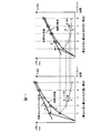
書き込みに関しては、書込み元のメモリ閾値電圧を書込み先に近づける、という手法を採用する。ここで採用する方式では、電圧パルスの印加形態は書き込み処理時間の短縮が考慮されたISPPを基本とする。先ずこの点から説明する。不揮発性メモリセルの書込み特性はメモリセル毎にバラツキが有る。図2のように書き込み電圧の印加時間に対してメモリ閾値電圧(メモリVth)の遷移が速い特性を示すもの(速い書き込み特性)、閾値電圧の遷移が遅い特性を示すもの(遅い書き込み特性)がある。そこで書込みメモリ閾値電圧分布幅を所望の範囲に揃える(すなわちメモリ閾値電圧分布の狭帯化をする)ために、書き込み処理は図3のように、書込みフローは書込みバイアスを加えメモリ閾値電圧を上昇させる「書込みバイアス印加」とメモリ閾値電圧が所望の電圧値まで上昇したか判定する「書込みベリファイ」の繰り返しからなる。書込み動作は全てのメモリセルが書込みベリファイをパスするまで、連続的に繰り返される。よって書込み動作時間を短縮するためには、この繰り返し回数を減らす事が有効である。
<Write method>
For writing, a technique of bringing the memory threshold voltage of the writing source closer to the writing destination is adopted. In the method adopted here, the application form of the voltage pulse is basically ISPP in consideration of shortening of the write processing time. First, this point will be described. The write characteristics of nonvolatile memory cells vary from memory cell to memory cell. As shown in FIG. 2, a memory threshold voltage (memory Vth) has a fast transition characteristic (fast write characteristic) and a threshold voltage has a slow transition characteristic (slow write characteristic) with respect to the write voltage application time. is there. Therefore, in order to align the write memory threshold voltage distribution width within the desired range (that is, to narrow the memory threshold voltage distribution), the write process increases the memory threshold voltage by adding a write bias as shown in FIG. “Write bias application” to be performed and “write verify” to determine whether the memory threshold voltage has increased to a desired voltage value are repeated. The write operation is continuously repeated until all memory cells pass the write verify. Therefore, in order to shorten the write operation time, it is effective to reduce the number of repetitions.
任意の書込みワード電圧(VWW)を加えた際のフラッシュメモリの書込み特性は、図4のように累積書込みバイアス印加時間の対数に対して線形である事が知られている。よって書込みパルス長を一定とすると、書込みパルス印加毎のメモリ閾値電圧(メモリVth)の増加量ΔVthが徐々に減少し、書込みベリファイ回数が増大する問題がある。そこでΔVthを一定にし、書込みベリファイ回数を最適化するために、図5のように書込みパルス毎に書込みバイアス印加時間を累積バイアス印加時間のべき乗に延ばす「べき乗パルス方式」がある。このべき乗パルス方式では、ベリファイ回数の最適化は可能だが書込みパルス毎にパルス長(=tWP)が延びるため、書込みバイアス印加時間(=ΣtWP)が指数的に増大する問題があった。 It is known that the write characteristics of the flash memory when an arbitrary write word voltage (VWW) is applied are linear with respect to the logarithm of the cumulative write bias application time as shown in FIG. Therefore, if the write pulse length is constant, there is a problem that the increase amount ΔVth of the memory threshold voltage (memory Vth) every time the write pulse is applied gradually decreases and the number of write verifications increases. Therefore, in order to make ΔVth constant and optimize the number of write verifications, there is a “power pulse method” in which the write bias application time is extended to the power of the cumulative bias application time for each write pulse as shown in FIG. In this power pulse method, the number of verifications can be optimized. However, since the pulse length (= tWP) increases for each write pulse, there is a problem that the write bias application time (= ΣtWP) increases exponentially.
書込みパルス毎にワード電圧VWWが一定であったべき乗パルス方式に対して、書込みパルス毎にパルス長を一定にするISPP方式がある。ISPP方式では、図6のように書込みバイアスをパルス毎にΔVwwだけ増加させ(VWWn+1=VWWn+ΔVww)、書込みパルス長を一定に保つ。これにより理想的にはメモリ閾値電圧はパルス印加毎にΔVwwだけ上昇するため、べき乗パルス方式と同様にベリファイ回数の最適化が可能となる。理想的な書込みベリファイ回数Nverifyは、書込み特性バラツキをΔVthwとすると、Nverify=ΔVthw/ΔVwwで与えられる。 In contrast to the power pulse method in which the word voltage VWW should be constant for each write pulse, there is an ISPP method in which the pulse length is constant for each write pulse. In the ISPP method, as shown in FIG. 6, the write bias is increased by ΔVww for each pulse (VWWn + 1 = VWWn + ΔVww), and the write pulse length is kept constant. Thus, ideally, the memory threshold voltage increases by ΔVww every time the pulse is applied, so that the number of verifications can be optimized in the same way as in the power pulse method. The ideal number of times of write verification Nverify is given by Nverify = ΔVthw / ΔVww, where the variation in write characteristics is ΔVthw.
図7図にはISPPを行った場合の実際の書込みベリファイ毎のメモリ閾値電圧の変動量ΔVthを示す。図7に示す通り、ワード電圧VWWが高い程ベリファイ回数の少ない領域でΔVthが大きくなる。このため、書込み動作の初期では書込みバラツキが大きくなり書込み飛び出し不良が発生しやすい。しかしこの対策としてワード電圧VWWを下げると、書込みベリファイをパスし難かったり、無駄な書込みバイアス電圧印加と書込みベリファイ回数が増大する問題がある。 FIG. 7 shows a variation amount ΔVth of the memory threshold voltage for each actual write verify when ISPP is performed. As shown in FIG. 7, as the word voltage VWW is higher, ΔVth is larger in a region where the number of verifications is smaller. For this reason, in the initial stage of the write operation, the write variation becomes large and a write jump defect is likely to occur. However, if the word voltage VWW is lowered as a countermeasure, there is a problem that it is difficult to pass the write verification, and the useless application of the write bias voltage and the number of write verifications are increased.
そこで、上述の認識の下で、書込み元のメモリ閾値電圧を書込み先に近づける、という手法を採用する。この手法は(1)低電圧側から書込みデータを合成しながら、順番に段階を踏んで書込みを行うというミックスプログラム(Mix Program)方式、(2)最初の書込みバイアス印加のみ粗く書込みを行う初期パルス印加方式に大別される。何れの場合も書込み元のメモリ閾値電圧を書込み先に近づける、という点で共通点を有している。 Therefore, based on the above recognition, a method of bringing the memory threshold voltage of the writing source closer to the writing destination is adopted. This method is (1) a mixed program (Mix Program) method in which write data is synthesized step by step while synthesizing write data from the low voltage side, and (2) an initial pulse for coarsely writing only the first write bias application. It is roughly divided into application methods. In any case, there is a common point in that the memory threshold voltage of the writing source is brought close to the writing destination.
《ミックスプログラム(Mix Program)方式》
ミックスプログラム方式とは、消去分布(11データ分布)のメモリ閾値電圧から、低電圧側の書込み分布に順番に書込みを行う方法である。ミックスプログラム方式では、各閾値電圧分布の書込みを行う際、図8の比較例のように書込み対象のメモリ閾値電圧毎に書込みを行う手法に対して、図9のように書込み対象分布より高電圧側の書込み分布も合わせて書込みを行うものである。図8の比較例と図9のミックスプログラム方式では書き込みデータに対する書き込み処理対象が図10に示される相違を有することになる。ミックスプログラム方式を採用すると、書込み元のメモリ閾値電圧分布は、必ず書込み先のメモリ閾値電圧分布の一つ低電圧側の分布となる。例えば各メモリ閾値電圧分布の間隔(電位差)が1V以下であっても、これに対する書込み特性バラツキは最大で閾値電圧分布の間隔に対して1.5倍程度になる。低電圧側から書込みを行う事で、本来の書込み特性バラツキよりもバラツキの小さい領域で書込みを行うことが可能になる。要するに、図2に示されるように、早い書き込み特性を持つメモリセルと遅い書き込み特性を持つメモリセルとの書き込み特性のバラツキは書き込み電圧の累計印加時間が長くなるに従って大きくなるから、遷移元(初期分布)に対して遷移先の閾値電圧がVHに対してVLのように近づく程書込み特性バラツキがDHからDLのように小さくなって、書込みベリファイ回数の抑制が可能になる。特に消去分布から高電圧側に離れた’01’分布、’00’分布の書込みベリファイ回数を抑制できる。例えば各々のベリファイ回数が2〜3回減らせる。書込み処理時間は1割程度の短縮になる。書込みベリファイ回数の低減は書込み処理時間の短縮に資するものとなる。図11には図2の内容を表現を変えて示している。
《Mix Program method》
The mixed program method is a method of sequentially writing from the memory threshold voltage of the erase distribution (11 data distribution) to the write distribution on the low voltage side. In the mixed program method, when writing each threshold voltage distribution, the method of writing for each memory threshold voltage to be written as in the comparative example of FIG. Writing is also performed in accordance with the writing distribution on the side. In the comparative example of FIG. 8 and the mixed program method of FIG. 9, the write processing target for the write data has the difference shown in FIG. When the mixed program method is employed, the memory threshold voltage distribution of the writing source is always one distribution on the low voltage side of the memory threshold voltage distribution of the writing destination. For example, even if the interval (potential difference) between the memory threshold voltage distributions is 1 V or less, the variation in the write characteristic with respect to this is at most about 1.5 times the interval of the threshold voltage distribution. By writing from the low voltage side, it is possible to perform writing in a region where the variation is smaller than the original variation in write characteristics. In short, as shown in FIG. 2, the variation in the write characteristic between the memory cell having the fast write characteristic and the memory cell having the slow write characteristic becomes larger as the cumulative application time of the write voltage becomes longer. As the threshold voltage of the transition destination approaches VL with respect to VH with respect to (distribution), the write characteristic variation decreases from DH to DL, and the number of write verifications can be suppressed. In particular, it is possible to suppress the number of write verifications of the “01” distribution and the “00” distribution that are separated from the erase distribution toward the high voltage side. For example, the number of times of each verification can be reduced by 2 to 3 times. The write processing time is reduced by about 10%. Reducing the number of times of write verification contributes to shortening of the write processing time. FIG. 11 shows the contents of FIG. 2 with different expressions.
《初期パルス印加方式》
書込み元と書込み先のメモリ閾値電圧の電位差を小さくするためには、最初の書込みバイアス印加(初期パルス印加)で、メモリ閾値電圧を出来るだけ書込み先に近づけるのがよい。そのためにはISPPのパルス幅を延ばすことが有効だが、全てのパルス幅を延ばすと総書込みバイアス時間が増加する問題がある。そこで、図12のように、初期パルスのみ、他の書込みパルスに対して、書込みバイアス印加時間を延ばす。すなわち、各閾値電圧分布における書き込み処理において最初の書込みバイアス印加のみ粗く書込みを行う。このように最初の書込みパルスのみ粗く書込みを行うことで、2発目以降の書込みパルス印加毎のメモリ閾値電圧の変化量を小さくできるため、書込み飛び出し不良の抑制が可能になり、これによって、書込みワード電圧を高めに設定できるようになり、書込み処理時間の短縮に資することができる。その理由を説明する。図13には不揮発性メモリセルMCの断面構造が例示される。CGはコントロールゲート、FGはフローティングゲート、VTNは書き込み時におけるトンネル酸化膜電位、VWWは書き込みゲート電圧である。書き込みでは電子(エレクトロン)がフローティングゲートFGに注入される。書き込みパルスを印加した後の時点において不揮発性メモリセルのフローティングゲートに蓄積された電子が少ない状態では基板とフローティングゲートとの間の電位差が比較的大きいままの状態であって、依然として電子がトンネル膜を抜け易い状態にあり、図14に示されるようにトンネル酸化膜電位VTNは大きい状態にある。この状態のメモリセルは遅い書き込み特性を持つメモリセルの特性と同じであると把握することができる。その逆に、不揮発性メモリセルのフローティングゲートFGに蓄積された電子が多い状態では基板とフローティングゲートFGとの間の電位差が比較的小さくなって、電子がトンネル膜を抜け難い状態にあり、図14に示されるようにトンネル酸化膜電位VTNは小さい状態にある。この状態のメモリセルは速い書き込み特性を持つメモリセルの特性と同じであると把握することができる。したがって、後者に比べて前者は、その次の書き込みパルスの印加によって飛び出し不良を生ずる蓋然性が高くなる。よって、最初の書込みパルス電圧印加(すなわち初期パルス電圧印加)で、メモリ閾値電圧を出来るだけ書込み先に近づける(換言すれば、初期パルス電圧印後における書込み元と書込み先のメモリ閾値電位差が小さくされる)ことにより、2パルス目以降は書込み元と書込み先のメモリ閾値電圧が近い領域で書込みを行えるようになり、書込み飛び出し不良率の低減、ひいては、書込み処理時間の短縮に資することができる。図15には飛び出し不良の概念が例示される。例えばINI−DSBを初期分布、REG−DSB1をその上の正規の閾値電圧分布、REG−DSB2を更にその上の正規の閾値電圧分布とする。VRiniは初期分布の閾値電圧を有するメモリセルに対する読み出しワード線電圧、VRdsb1は閾値電圧分布REG−DSB1の閾値電圧を有するメモリセルに対する読み出しワード線電圧である。例えば閾値電圧分布REG−DSB1に入れることを目的とする書き込み処理における飛び出し不良とは、メモリセルの閾値電圧が読み出しワード線電圧VRdsb1を越えてしまうことである。IREG−DSB1が正規の閾値電圧分布REG−DSB1に対する飛び出し不良分布の一例となる。
<Initial pulse application method>
In order to reduce the potential difference between the memory threshold voltage of the write source and the write destination, it is preferable to bring the memory threshold voltage as close as possible to the write destination by applying the first write bias (initial pulse application). For this purpose, it is effective to increase the pulse width of ISPP, but if all the pulse widths are extended, there is a problem that the total write bias time increases. Therefore, as shown in FIG. 12, the write bias application time is extended for only the initial pulse and other write pulses. That is, writing is performed roughly only in the first write bias application in the writing process in each threshold voltage distribution. By roughly writing only the first write pulse in this way, the amount of change in the memory threshold voltage for each application of the second and subsequent write pulses can be reduced, thereby making it possible to suppress write popping defects. The word voltage can be set higher, which can contribute to shortening the write processing time. The reason will be explained. FIG. 13 illustrates a cross-sectional structure of the nonvolatile memory cell MC. CG is a control gate, FG is a floating gate, VTN is a tunnel oxide film potential at the time of writing, and VWW is a writing gate voltage. In writing, electrons (electrons) are injected into the floating gate FG. When the number of electrons accumulated in the floating gate of the nonvolatile memory cell at the time after applying the write pulse is small, the potential difference between the substrate and the floating gate remains relatively large, and the electrons still remain in the tunnel film. As shown in FIG. 14, the tunnel oxide film potential VTN is in a large state. It can be understood that the memory cell in this state has the same characteristics as a memory cell having a slow write characteristic. Conversely, in a state where there are many electrons accumulated in the floating gate FG of the nonvolatile memory cell, the potential difference between the substrate and the floating gate FG becomes relatively small, and it is difficult for the electrons to pass through the tunnel film. As shown in FIG. 14, the tunnel oxide film potential VTN is in a small state. It can be understood that the memory cell in this state has the same characteristics as a memory cell having a fast write characteristic. Therefore, compared to the latter, the former is more likely to cause a pop-out defect due to the application of the next write pulse. Therefore, the memory threshold voltage is brought as close as possible to the writing destination by applying the first writing pulse voltage (that is, applying the initial pulse voltage) (in other words, the memory threshold potential difference between the writing source and the writing destination after the initial pulse voltage is applied is reduced). Thus, after the second pulse, writing can be performed in an area where the memory threshold voltages of the writing source and the writing destination are close to each other, which can contribute to the reduction of the write-out failure rate and hence the writing processing time. FIG. 15 illustrates the concept of pop-out failure. For example, INI-DSB is an initial distribution, REG-DSB1 is a normal threshold voltage distribution above it, and REG-DSB2 is a normal threshold voltage distribution above it. VRini is a read word line voltage for a memory cell having an initial distribution threshold voltage, and VRdsb1 is a read word line voltage for a memory cell having a threshold voltage of threshold voltage distribution REG-DSB1. For example, the pop-out defect in the write processing intended to be included in the threshold voltage distribution REG-DSB1 is that the threshold voltage of the memory cell exceeds the read word line voltage VRdsb1. IREG-DSB1 is an example of a pop-out defect distribution with respect to the normal threshold voltage distribution REG-DSB1.
前記ミックスプログラム方式は書込み先のメモリ閾値電圧分布の決定に関するものであり、初期パルス印加方式は書込みバイアスの印加の方法に関するものであり、各々の具体的手段は相違するから、相互に組み合わせて用いる事ができる。図16にはそれらを組み合わせて用いたときの書き込みゲート電圧VWWと飛び出し不良率及び書き込みベリファイ回数との関係が例示される。ベリファイ回数は前記比較例方式に比べてミックスプログラム方式の方が少なくなり、飛び出し不良率は初期パルスなしの場に比べて初期パルス方式を用いた方が低下される。例えば初期パルス方式を採用しない場合に飛び出し不良をゼロにしたい場合には書き込みゲート電圧VWWをV1に設定しなければならず、このとき、比較例方式を用いないなら、書き込みベリファイ回数はN1となり、ミックスプログラム方式を採用すればN2となる。初期パルス方式とミックスプログラム方式の双方を採用すれば書き込みゲート電圧VWWをV2に高くしても書き込み不良率をゼロに保ったまま書き込みベリファイ回数をN3に減ずることができる。 The mixed program method relates to the determination of the memory threshold voltage distribution of the write destination, and the initial pulse application method relates to the method of applying the write bias. Since the specific means are different, they are used in combination with each other. I can do things. FIG. 16 illustrates the relationship between the write gate voltage VWW, the pop-out defect rate, and the write verify count when they are used in combination. The number of times of verification is smaller in the mixed program method than in the comparative example method, and the pop-out failure rate is lower in the case of using the initial pulse method than in the case without the initial pulse. For example, when the initial pulse method is not adopted and the pop-out defect is desired to be zero, the write gate voltage VWW must be set to V1. At this time, if the comparative example method is not used, the number of write verify times is N1. If the mix program method is adopted, N2 is obtained. If both the initial pulse method and the mixed program method are employed, even if the write gate voltage VWW is increased to V2, the number of write verify operations can be reduced to N3 while maintaining the write defect rate at zero.
前記ミックスプログラム方式によれば所謂ソース浮きの効果を更に期待することができる。即ち、読み出し動作では、ビット線の充放電による電圧センスを行っている。そのためソース線を共通とするような小領域のメモリセルのメモリ閾値電圧に着目すると、そのような小領域の他のメモリセルに追加書込み等により書き込みが行われると、読み出し動作時に当該ソース線に全体として流れる読み出し電流が少なくなって、読み出しメモリセル電流によるソース電位の浮きの減少により、メモリ閾値電圧が下がって見える。同じ原因で、書込み動作初期に書き込みパスしたメモリセルは書込み動作が進むにつれて徐々にメモリ閾値電圧が下がって見える。さらに低電圧側のメモリ閾値電圧分布から書込むことで、高電圧側から書込む場合と比較してこの効果は大きくなると考えられる。書込み飛び出しし易い、書込みパルス回数の少ない領域で書込みベリファイをパスしたメモリセルは、前記ソース浮きの効果により、メモリ閾値電圧が低電圧側にシフトする。これは、前記ソース浮きの効果が飛び出し不良を抑制する方向に作用することを意味する。 According to the mix program method, the so-called source floating effect can be further expected. That is, in the read operation, voltage sensing is performed by charging / discharging the bit line. Therefore, paying attention to the memory threshold voltage of a memory cell in a small area that shares a source line, if writing is performed to another memory cell in such a small area by additional writing or the like, The read current flowing as a whole decreases, and the memory threshold voltage appears to decrease due to the decrease in floating of the source potential due to the read memory cell current. For the same reason, the memory threshold voltage of the memory cell that has passed the write operation at the beginning of the write operation appears to gradually decrease as the write operation proceeds. Furthermore, writing from the memory threshold voltage distribution on the low voltage side is considered to increase this effect as compared to writing from the high voltage side. The memory threshold voltage of the memory cell that has passed the write verify in the region where the number of write pulses is small and is likely to jump out of the memory shifts to the low voltage side due to the effect of the floating source. This means that the effect of the source floating acts in a direction to suppress the pop-out defect.
図17には初期パルス印加方式の別の例が示される。ここでは、前記メモリセルトランジスタの閾値電圧を初期分布から目的の閾値電圧分布に変更するとき、メモリセルトランジスタのワード線に印加する書き込み電圧パルスの電圧レベルを最初のパルスを除いて順次高くし、且つ、パルス幅を最初のパルスを除いて一定とし、最初のパルス幅をそれ以降のパルス幅よりも大きくする。電圧パルスの印加形態は同じくISPPを基本とする。更に詳しくは、初期パルスのバイアス時間を延ばすのではなく初期パルスのVWWだけISPPから外して任意の高電圧に設定する。これはパルス時間の短縮が可能という点で、書込み動作の高速化に適している。 FIG. 17 shows another example of the initial pulse application method. Here, when the threshold voltage of the memory cell transistor is changed from the initial distribution to the target threshold voltage distribution, the voltage level of the write voltage pulse applied to the word line of the memory cell transistor is sequentially increased except for the first pulse, In addition, the pulse width is constant except for the first pulse, and the first pulse width is made larger than the subsequent pulse width. The application form of the voltage pulse is basically based on ISPP. More specifically, instead of extending the bias time of the initial pulse, only the VWW of the initial pulse is removed from the ISPP and set to an arbitrary high voltage. This is suitable for speeding up the write operation because the pulse time can be shortened.
図18には初期パルス印加方式の更に別の例が示される。ここでは、前記メモリセルトランジスタの閾値電圧を初期分布から目的の閾値電圧分布に変更するとき、メモリセルトランジスタのワード線に印加する書き込み電圧パルスの電圧レベルを順次高くし、且つ、閾値電圧単位のパルス幅を最初のパルスから順次小さくする。電圧パルスの印加形態は同じくISPPを基本とする。要するに、初期パルスのバイアス時間を延ばすと共に、2回目以降の書込みバイアス印加毎に徐々にバイアス印加時間を短くすることで、より飛び出し不良を生じ難くしたものである。 FIG. 18 shows still another example of the initial pulse application method. Here, when the threshold voltage of the memory cell transistor is changed from the initial distribution to the target threshold voltage distribution, the voltage level of the write voltage pulse applied to the word line of the memory cell transistor is sequentially increased, and the threshold voltage unit. The pulse width is sequentially reduced from the first pulse. The application form of the voltage pulse is basically based on ISPP. In short, by extending the bias time of the initial pulse and gradually shortening the bias application time for each second and subsequent write bias application, it becomes more difficult to cause pop-out defects.
以上本発明者によってなされた発明を実施形態に基づいて具体的に説明したが、本発明はそれに限定されるものではなく、その要旨を逸脱しない範囲において種々変更可能であることは言うまでもない。 Although the invention made by the present inventor has been specifically described based on the embodiments, it is needless to say that the present invention is not limited thereto and can be variously modified without departing from the gist thereof.
例えば、上記では書き込み制御は制御部CNTが行うが、データプロセッサなどメモリの外部ロジックで行う等にしてもよい。また、上記説明ではフローティングゲートを用いたメモリセルに適用した場合を説明したが、シリコンナイトライド膜を電荷蓄積領域に用いるメモリセルにも本発明は適用可能である。更に多値記憶は4値に限定されず、それ以上の8値記憶にも本発明は適用可能である。本発明は単体の不揮発性メモリはもとよりマイクロコンピュータなどのオンチップの不揮発性メモリなどに広く適用することができる。 For example, in the above, the write control is performed by the control unit CNT, but may be performed by an external logic of a memory such as a data processor. In the above description, the case where the present invention is applied to a memory cell using a floating gate has been described. However, the present invention can also be applied to a memory cell using a silicon nitride film for a charge storage region. Further, multi-value storage is not limited to four values, and the present invention can be applied to more eight-value storage. The present invention can be widely applied not only to a single nonvolatile memory but also to an on-chip nonvolatile memory such as a microcomputer.
1 フラッシュメモリ
FARY0〜FARY3 フラッシュメモリアレイ
CNT 制御部
MC 不揮発性メモリセル
1 Flash memory FARY0 to FARY3 Flash memory array CNT control unit MC Nonvolatile memory cell
Claims (8)
前記メモリアレイは、電気的に閾値電圧を変更可能にされる複数のメモリトランジスタを有し、
前記制御回路は、閾値電圧の変更によって1個の前記メモリセルトランジスタに4値以上の論理値を記憶可能とし、
前記制御回路は、前記メモリセルトランジスタの閾値電圧を初期分布から目的の閾値電圧分布に変更するとき、変更対象とされる全ての前記メモリセルトランジスタについて、初期分布側から目的の閾値電圧分布に至るまで順次閾値電圧分布単位で閾値電圧を遷移させると共に、閾値電圧を遷移させるときメモリセルトランジスタのワード線に印加する書き込み電圧のパルス幅と電圧レベルとの積が最初のパルス印加で最大になるように制御する不揮発性記憶装置。 A memory array and a control circuit;
The memory array includes a plurality of memory transistors whose threshold voltage can be electrically changed,
The control circuit can store four or more logic values in one memory cell transistor by changing a threshold voltage;
When the threshold voltage of the memory cell transistor is changed from the initial distribution to the target threshold voltage distribution, the control circuit reaches the target threshold voltage distribution from the initial distribution side for all the memory cell transistors to be changed. The threshold voltage is sequentially changed in units of threshold voltage distribution until the threshold voltage is changed, and the product of the pulse width of the write voltage applied to the word line of the memory cell transistor and the voltage level is maximized by the first pulse application. Nonvolatile storage device to control.
前記メモリアレイは、電気的に閾値電圧を変更可能にされる複数のメモリトランジスタを有し、
前記制御回路は、閾値電圧の変更によって1個の前記メモリセルトランジスタに4値以上の論理値を記憶可能とし、
前記制御回路は、前記メモリセルトランジスタの閾値電圧を初期分布から目的の閾値電圧分布に変更するとき、変更対象とされる全ての前記メモリセルトランジスタについて順次目的とする閾値電圧分布へ遷移させると共に、閾値電圧を遷移させるときメモリセルトランジスタに印加する書き込み電圧のパルス幅と電圧レベルとの積が最初のパルス印加で最大になるように制御する不揮発性記憶装置。 A memory array and a control circuit;
The memory array includes a plurality of memory transistors whose threshold voltage can be electrically changed,
The control circuit can store four or more logic values in one memory cell transistor by changing a threshold voltage;
When the control circuit changes the threshold voltage of the memory cell transistor from the initial distribution to the target threshold voltage distribution, the control circuit sequentially makes a transition to the target threshold voltage distribution for all the memory cell transistors to be changed, and A non-volatile memory device that controls a product of a pulse width and a voltage level of a write voltage to be applied to a memory cell transistor when a threshold voltage is changed to be maximized by the first pulse application.
Priority Applications (1)
| Application Number | Priority Date | Filing Date | Title |
|---|---|---|---|
| JP2004376486A JP2006185483A (en) | 2004-12-27 | 2004-12-27 | Nonvolatile storage apparatus |
Applications Claiming Priority (1)
| Application Number | Priority Date | Filing Date | Title |
|---|---|---|---|
| JP2004376486A JP2006185483A (en) | 2004-12-27 | 2004-12-27 | Nonvolatile storage apparatus |
Publications (1)
| Publication Number | Publication Date |
|---|---|
| JP2006185483A true JP2006185483A (en) | 2006-07-13 |
Family
ID=36738495
Family Applications (1)
| Application Number | Title | Priority Date | Filing Date |
|---|---|---|---|
| JP2004376486A Withdrawn JP2006185483A (en) | 2004-12-27 | 2004-12-27 | Nonvolatile storage apparatus |
Country Status (1)
| Country | Link |
|---|---|
| JP (1) | JP2006185483A (en) |
Cited By (5)
| Publication number | Priority date | Publication date | Assignee | Title |
|---|---|---|---|---|
| JP2008117508A (en) * | 2006-11-03 | 2008-05-22 | Hynix Semiconductor Inc | Method for setting programming start bias for flash memory device and programming method using the same |
| JP2008198337A (en) * | 2007-01-17 | 2008-08-28 | Toshiba Corp | Semiconductor storage device |
| JP2009048760A (en) * | 2007-08-22 | 2009-03-05 | Samsung Electronics Co Ltd | Programming method for nonvolatile memory |
| JP2010020880A (en) * | 2008-07-10 | 2010-01-28 | Hynix Semiconductor Inc | Programming method of nonvolatile memory device |
| US11514984B2 (en) | 2019-09-19 | 2022-11-29 | Kioxia Corporation | Semiconductor memory device executing program operation |
-
2004
- 2004-12-27 JP JP2004376486A patent/JP2006185483A/en not_active Withdrawn
Cited By (6)
| Publication number | Priority date | Publication date | Assignee | Title |
|---|---|---|---|---|
| JP2008117508A (en) * | 2006-11-03 | 2008-05-22 | Hynix Semiconductor Inc | Method for setting programming start bias for flash memory device and programming method using the same |
| JP2008198337A (en) * | 2007-01-17 | 2008-08-28 | Toshiba Corp | Semiconductor storage device |
| JP2009048760A (en) * | 2007-08-22 | 2009-03-05 | Samsung Electronics Co Ltd | Programming method for nonvolatile memory |
| KR101373186B1 (en) | 2007-08-22 | 2014-03-13 | 삼성전자주식회사 | Flash memory device and program methods thereof, and memory system and computer system including the same |
| JP2010020880A (en) * | 2008-07-10 | 2010-01-28 | Hynix Semiconductor Inc | Programming method of nonvolatile memory device |
| US11514984B2 (en) | 2019-09-19 | 2022-11-29 | Kioxia Corporation | Semiconductor memory device executing program operation |
Similar Documents
| Publication | Publication Date | Title |
|---|---|---|
| US9852788B2 (en) | Multipage program scheme for flash memory | |
| JP4038823B2 (en) | Semiconductor nonvolatile memory device and computer system using the same | |
| US8565020B2 (en) | Semiconductor memory device | |
| US8174899B2 (en) | Non-volatile semiconductor memory device | |
| US7619920B2 (en) | NAND type flash memory and write method of the same | |
| US20100172181A1 (en) | Page buffer circuit for electrically rewritable non-volatile semiconductor memory device and control method | |
| US8848447B2 (en) | Nonvolatile semiconductor memory device using write pulses with different voltage gradients | |
| WO2009081745A1 (en) | Nonvolatile semiconductor storage device | |
| US20190035481A1 (en) | Memory device and method of operating the same | |
| US6826081B2 (en) | Nonvolatile semiconductor memory device, nonvolatile semiconductor memory device-integrated system, and defective block detecting method | |
| US6661709B2 (en) | Nonvolatile semiconductor memory device | |
| JP2011086364A (en) | Non-volatile semiconductor storage device | |
| US8189394B2 (en) | Page buffer circuit of nonvolatile memory device and method of operating the same | |
| US5812451A (en) | Nonvolatile semiconductor storage apparatus and method of writing data to the same | |
| US20090055579A1 (en) | Semiconductor memory device for simultaneously programming plurality of banks | |
| JP6677786B1 (en) | Page buffer circuit and nonvolatile storage device | |
| JP2011233209A (en) | Semiconductor storage | |
| US8238156B2 (en) | Nonvolatile semiconductor memory device and method of operating the same | |
| KR100866957B1 (en) | Nonvolatile memory device with shortened data program time and driving method thereof | |
| JP2006185483A (en) | Nonvolatile storage apparatus | |
| JP5787921B2 (en) | Nonvolatile semiconductor memory device | |
| US6487115B1 (en) | Non-volatile semiconductor memory device with writing sequence enabling early-stage judgement of writing | |
| JP3698462B2 (en) | Semiconductor nonvolatile memory device and computer system using the same | |
| KR100904731B1 (en) | Page Buffer and Program Method for Multi-Level Cell Flash Memory Devices | |
| JP3519542B2 (en) | Semiconductor storage device |
Legal Events
| Date | Code | Title | Description |
|---|---|---|---|
| A300 | Withdrawal of application because of no request for examination |
Free format text: JAPANESE INTERMEDIATE CODE: A300 Effective date: 20080304 |