JP2006146219A - Display device and driving method thereof - Google Patents
Display device and driving method thereof Download PDFInfo
- Publication number
- JP2006146219A JP2006146219A JP2005330899A JP2005330899A JP2006146219A JP 2006146219 A JP2006146219 A JP 2006146219A JP 2005330899 A JP2005330899 A JP 2005330899A JP 2005330899 A JP2005330899 A JP 2005330899A JP 2006146219 A JP2006146219 A JP 2006146219A
- Authority
- JP
- Japan
- Prior art keywords
- voltage
- driving transistor
- light emitting
- transistor
- terminal
- Prior art date
- Legal status (The legal status is an assumption and is not a legal conclusion. Google has not performed a legal analysis and makes no representation as to the accuracy of the status listed.)
- Granted
Links
Images


Classifications
-
- G—PHYSICS
- G09—EDUCATION; CRYPTOGRAPHY; DISPLAY; ADVERTISING; SEALS
- G09G—ARRANGEMENTS OR CIRCUITS FOR CONTROL OF INDICATING DEVICES USING STATIC MEANS TO PRESENT VARIABLE INFORMATION
- G09G3/00—Control arrangements or circuits, of interest only in connection with visual indicators other than cathode-ray tubes
- G09G3/20—Control arrangements or circuits, of interest only in connection with visual indicators other than cathode-ray tubes for presentation of an assembly of a number of characters, e.g. a page, by composing the assembly by combination of individual elements arranged in a matrix no fixed position being assigned to or needed to be assigned to the individual characters or partial characters
- G09G3/22—Control arrangements or circuits, of interest only in connection with visual indicators other than cathode-ray tubes for presentation of an assembly of a number of characters, e.g. a page, by composing the assembly by combination of individual elements arranged in a matrix no fixed position being assigned to or needed to be assigned to the individual characters or partial characters using controlled light sources
- G09G3/30—Control arrangements or circuits, of interest only in connection with visual indicators other than cathode-ray tubes for presentation of an assembly of a number of characters, e.g. a page, by composing the assembly by combination of individual elements arranged in a matrix no fixed position being assigned to or needed to be assigned to the individual characters or partial characters using controlled light sources using electroluminescent panels
- G09G3/32—Control arrangements or circuits, of interest only in connection with visual indicators other than cathode-ray tubes for presentation of an assembly of a number of characters, e.g. a page, by composing the assembly by combination of individual elements arranged in a matrix no fixed position being assigned to or needed to be assigned to the individual characters or partial characters using controlled light sources using electroluminescent panels semiconductive, e.g. using light-emitting diodes [LED]
- G09G3/3208—Control arrangements or circuits, of interest only in connection with visual indicators other than cathode-ray tubes for presentation of an assembly of a number of characters, e.g. a page, by composing the assembly by combination of individual elements arranged in a matrix no fixed position being assigned to or needed to be assigned to the individual characters or partial characters using controlled light sources using electroluminescent panels semiconductive, e.g. using light-emitting diodes [LED] organic, e.g. using organic light-emitting diodes [OLED]
- G09G3/3225—Control arrangements or circuits, of interest only in connection with visual indicators other than cathode-ray tubes for presentation of an assembly of a number of characters, e.g. a page, by composing the assembly by combination of individual elements arranged in a matrix no fixed position being assigned to or needed to be assigned to the individual characters or partial characters using controlled light sources using electroluminescent panels semiconductive, e.g. using light-emitting diodes [LED] organic, e.g. using organic light-emitting diodes [OLED] using an active matrix
- G09G3/3233—Control arrangements or circuits, of interest only in connection with visual indicators other than cathode-ray tubes for presentation of an assembly of a number of characters, e.g. a page, by composing the assembly by combination of individual elements arranged in a matrix no fixed position being assigned to or needed to be assigned to the individual characters or partial characters using controlled light sources using electroluminescent panels semiconductive, e.g. using light-emitting diodes [LED] organic, e.g. using organic light-emitting diodes [OLED] using an active matrix with pixel circuitry controlling the current through the light-emitting element
-
- G—PHYSICS
- G09—EDUCATION; CRYPTOGRAPHY; DISPLAY; ADVERTISING; SEALS
- G09G—ARRANGEMENTS OR CIRCUITS FOR CONTROL OF INDICATING DEVICES USING STATIC MEANS TO PRESENT VARIABLE INFORMATION
- G09G2300/00—Aspects of the constitution of display devices
- G09G2300/08—Active matrix structure, i.e. with use of active elements, inclusive of non-linear two terminal elements, in the pixels together with light emitting or modulating elements
- G09G2300/0809—Several active elements per pixel in active matrix panels
- G09G2300/0819—Several active elements per pixel in active matrix panels used for counteracting undesired variations, e.g. feedback or autozeroing
-
- G—PHYSICS
- G09—EDUCATION; CRYPTOGRAPHY; DISPLAY; ADVERTISING; SEALS
- G09G—ARRANGEMENTS OR CIRCUITS FOR CONTROL OF INDICATING DEVICES USING STATIC MEANS TO PRESENT VARIABLE INFORMATION
- G09G2300/00—Aspects of the constitution of display devices
- G09G2300/08—Active matrix structure, i.e. with use of active elements, inclusive of non-linear two terminal elements, in the pixels together with light emitting or modulating elements
- G09G2300/0809—Several active elements per pixel in active matrix panels
- G09G2300/0842—Several active elements per pixel in active matrix panels forming a memory circuit, e.g. a dynamic memory with one capacitor
- G09G2300/0861—Several active elements per pixel in active matrix panels forming a memory circuit, e.g. a dynamic memory with one capacitor with additional control of the display period without amending the charge stored in a pixel memory, e.g. by means of additional select electrodes
-
- G—PHYSICS
- G09—EDUCATION; CRYPTOGRAPHY; DISPLAY; ADVERTISING; SEALS
- G09G—ARRANGEMENTS OR CIRCUITS FOR CONTROL OF INDICATING DEVICES USING STATIC MEANS TO PRESENT VARIABLE INFORMATION
- G09G2310/00—Command of the display device
- G09G2310/02—Addressing, scanning or driving the display screen or processing steps related thereto
- G09G2310/0243—Details of the generation of driving signals
- G09G2310/0251—Precharge or discharge of pixel before applying new pixel voltage
-
- G—PHYSICS
- G09—EDUCATION; CRYPTOGRAPHY; DISPLAY; ADVERTISING; SEALS
- G09G—ARRANGEMENTS OR CIRCUITS FOR CONTROL OF INDICATING DEVICES USING STATIC MEANS TO PRESENT VARIABLE INFORMATION
- G09G2310/00—Command of the display device
- G09G2310/02—Addressing, scanning or driving the display screen or processing steps related thereto
- G09G2310/0243—Details of the generation of driving signals
- G09G2310/0254—Control of polarity reversal in general, other than for liquid crystal displays
-
- G—PHYSICS
- G09—EDUCATION; CRYPTOGRAPHY; DISPLAY; ADVERTISING; SEALS
- G09G—ARRANGEMENTS OR CIRCUITS FOR CONTROL OF INDICATING DEVICES USING STATIC MEANS TO PRESENT VARIABLE INFORMATION
- G09G2320/00—Control of display operating conditions
- G09G2320/04—Maintaining the quality of display appearance
- G09G2320/043—Preventing or counteracting the effects of ageing
-
- G—PHYSICS
- G09—EDUCATION; CRYPTOGRAPHY; DISPLAY; ADVERTISING; SEALS
- G09G—ARRANGEMENTS OR CIRCUITS FOR CONTROL OF INDICATING DEVICES USING STATIC MEANS TO PRESENT VARIABLE INFORMATION
- G09G2330/00—Aspects of power supply; Aspects of display protection and defect management
- G09G2330/02—Details of power systems and of start or stop of display operation
- G09G2330/021—Power management, e.g. power saving
Landscapes
- Engineering & Computer Science (AREA)
- Physics & Mathematics (AREA)
- Computer Hardware Design (AREA)
- General Physics & Mathematics (AREA)
- Theoretical Computer Science (AREA)
- Control Of Indicators Other Than Cathode Ray Tubes (AREA)
- Electroluminescent Light Sources (AREA)
- Control Of El Displays (AREA)
Abstract
【課題】非晶質シリコン薄膜トランジスタ及び有機発光素子の敷居電圧の劣化を補償することができ、電力損失を最小化することができる表示装置及びその駆動方法を提供する。
【解決手段】発光素子と、キャパシタと、制御端子、入力端子、及び出力端子を有し、発光素子が発光するように発光素子に駆動電流を供給する駆動トランジスタと、走査信号に応じて駆動トランジスタをダイオード接続させ、データ電圧をキャパシタに供給する第1スイッチング部と、発光信号に応じて駆動電圧を駆動トランジスタに供給し、キャパシタを駆動トランジスタに接続する第2スイッチング部とを各々含む複数の画素を有し、キャパシタは、第1スイッチング部を介して駆動トランジスタに接続されて、データ電圧と駆動トランジスタの敷居電圧に依存する制御電圧とを保存し、第2スイッチング部を介して駆動トランジスタに接続されて制御電圧を駆動トランジスタに供給する。
【選択図】図2A display device and a driving method thereof that can compensate for deterioration of the threshold voltage of an amorphous silicon thin film transistor and an organic light emitting device and can minimize power loss.
A driving transistor having a light emitting element, a capacitor, a control terminal, an input terminal, and an output terminal and supplying a driving current to the light emitting element so that the light emitting element emits light, and a driving transistor according to a scanning signal A plurality of pixels each including a first switching unit that supplies a data voltage to the capacitor and a second switching unit that supplies a driving voltage to the driving transistor according to the light emission signal and connects the capacitor to the driving transistor. The capacitor is connected to the driving transistor through the first switching unit, stores the data voltage and the control voltage depending on the threshold voltage of the driving transistor, and is connected to the driving transistor through the second switching unit. Then, a control voltage is supplied to the driving transistor.
[Selection] Figure 2
Description
本発明は、表示装置及びその駆動方法に関し、特に、非晶質シリコン薄膜トランジスタ及び有機発光素子の敷居電圧の劣化を補償することができ、電力損失を最小化することができる表示装置及びその駆動方法に関する。 The present invention relates to a display device and a driving method thereof, and more particularly to a display device capable of compensating for deterioration of a threshold voltage of an amorphous silicon thin film transistor and an organic light emitting element and minimizing power loss and a driving method thereof. About.
近年、パーソナルコンピュータやテレビなどの軽量化及び薄形化に伴って表示装置も軽量化及び薄形化が要求されており、このような要求によって陰極線管(CRT)が平板表示装置に代替されている。
このような平板表示装置には、液晶表示装置(LCD)、電界放出表示装置(FED)、有機発光表示装置、プラズマ表示装置(PDP)などがある。
In recent years, with the reduction in weight and thickness of personal computers and televisions, display devices have also been required to be reduced in weight and thickness. With such demands, cathode ray tubes (CRT) have been replaced with flat panel display devices. Yes.
Examples of such a flat panel display include a liquid crystal display (LCD), a field emission display (FED), an organic light emitting display, and a plasma display (PDP).
一般的に、能動型平板表示装置では複数の画素が行列形態に配列され、与えられた輝度情報に応じて各画素の光強度を制御することによって画像を表示する。このうちの有機発光表示装置は、蛍光性有機物質を電気的に励起発光させて画像を表示する表示装置であって、自己発光型であって消費電力が小さく、視野角が広く、画素の応答速度が速いので、高画質の動画像を表示するのが容易である。 In general, in an active flat panel display, a plurality of pixels are arranged in a matrix form, and an image is displayed by controlling the light intensity of each pixel in accordance with given luminance information. Among these, the organic light emitting display device is a display device that displays an image by electrically exciting and emitting a fluorescent organic substance, and is self-luminous, has low power consumption, a wide viewing angle, and a pixel response. Since the speed is fast, it is easy to display a high-quality moving image.
有機発光表示装置は、有機発光素子(OLED)とこれを駆動する薄膜トランジスタ(TFT)を備える。この薄膜トランジスタは、活性層の種類によって多結晶シリコン薄膜トランジスタと非晶質シリコン薄膜トランジスタなどに区分される。多結晶シリコン薄膜トランジスタを採用した有機発光表示装置は多様な長所があって一般的に広く使用されているが、薄膜トランジスタの製造工程が複雑であるために製造費用も増加する。また、このような有機発光表示装置では大画面のものを製造することは難しい。 The organic light emitting display device includes an organic light emitting element (OLED) and a thin film transistor (TFT) for driving the organic light emitting element (OLED). This thin film transistor is classified into a polycrystalline silicon thin film transistor and an amorphous silicon thin film transistor depending on the type of the active layer. An organic light emitting display using a polycrystalline silicon thin film transistor has various advantages and is generally widely used. However, a manufacturing process of the thin film transistor is complicated, and thus the manufacturing cost increases. In addition, it is difficult to manufacture a large-screen organic light-emitting display device.
一方、非晶質シリコン薄膜トランジスタを採用した有機発光表示装置は、大画面のものを製造し易く、多結晶シリコン薄膜トランジスタを採用した有機発光表示装置より製造工程の数も相対的に少ない。しかし、非晶質シリコン薄膜トランジスタが有機発光素子に持続的に電流を供給することにより、非晶質シリコン薄膜トランジスタ自体の敷居電圧(Vth)が遷移して劣化する恐れがある。これは、同一なデータ電圧が印加されても不均一な電流が有機発光素子に流れるようになり、結局、これによって有機発光表示装置の画質劣化が発生するという問題があった。 On the other hand, an organic light emitting display using an amorphous silicon thin film transistor is easy to manufacture a large screen, and the number of manufacturing steps is relatively smaller than that of an organic light emitting display using a polycrystalline silicon thin film transistor. However, when the amorphous silicon thin film transistor continuously supplies current to the organic light emitting device, the threshold voltage (V th ) of the amorphous silicon thin film transistor itself may transition and deteriorate. As a result, even when the same data voltage is applied, a non-uniform current flows through the organic light emitting device, resulting in a deterioration in image quality of the organic light emitting display device.
有機発光素子も長時間電流を流すことによってその敷居電圧が遷移する。n型薄膜トランジスタの場合、有機発光素子は薄膜トランジスタのソース側に位置するため、有機発光素子の敷居電圧が劣化すると薄膜トランジスタのソース方向電圧が変動する。そのため、薄膜トランジスタのゲートに同一なデータ電圧が印加されても、薄膜トランジスタのゲートとソースとの間の電圧が変動するので、不均一な電流が有機発光素子に流れるようになる。これも有機発光表示装置の画質劣化の一つの要因になる。 The threshold voltage of the organic light emitting element is also changed by passing a current for a long time. In the case of an n-type thin film transistor, since the organic light emitting element is located on the source side of the thin film transistor, the source direction voltage of the thin film transistor varies when the threshold voltage of the organic light emitting element deteriorates. For this reason, even if the same data voltage is applied to the gate of the thin film transistor, the voltage between the gate and the source of the thin film transistor fluctuates, so that a non-uniform current flows through the organic light emitting device. This is also a factor in image quality deterioration of the organic light emitting display device.
一方、駆動トランジスタ及び有機発光素子の敷居電圧の劣化を補償するために駆動電圧と有機発光素子との間の電流経路に多くの数の薄膜トランジスタを接続する場合、これらによって電力の損失が大きくなってしまうという問題があった。 On the other hand, when a large number of thin film transistors are connected to the current path between the driving voltage and the organic light emitting device in order to compensate for the deterioration of the threshold voltage of the driving transistor and the organic light emitting device, power loss increases due to these. There was a problem that.
そこで、本発明は上記従来の表示装置及びその駆動方法における問題点に鑑みてなされたものであって、本発明の目的は、非晶質シリコン薄膜トランジスタを備えながらも非晶質シリコン薄膜トランジスタ及び有機発光素子の敷居電圧の劣化を補償することができ、電力損失を最小化することができる表示装置及びその駆動方法を提供することにある。 Therefore, the present invention has been made in view of the problems in the conventional display device and the driving method thereof, and an object of the present invention is to provide an amorphous silicon thin film transistor and an organic light emitting device while including the amorphous silicon thin film transistor. It is an object of the present invention to provide a display device that can compensate for deterioration of the threshold voltage of an element and minimize power loss, and a driving method thereof.
上記目的を達成するためになされた本発明による表示装置は、発光素子と、キャパシタと、制御端子、入力端子、及び出力端子を有し、前記発光素子が発光するように発光素子に駆動電流を供給する駆動トランジスタと、走査信号に応じて前記駆動トランジスタをダイオード接続させ、データ電圧を前記キャパシタに供給する第1スイッチング部と、発光信号に応じて駆動電圧を前記駆動トランジスタに供給し、前記キャパシタを前記駆動トランジスタに接続する第2スイッチング部とを各々含む複数の画素を有し、前記キャパシタは、前記第1スイッチング部を介して前記駆動トランジスタに接続されて、前記データ電圧と前記駆動トランジスタの敷居電圧に依存する制御電圧とを保存し、前記第2スイッチング部を介して前記駆動トランジスタに接続されて前記制御電圧を前記駆動トランジスタに供給することを特徴とする。 A display device according to the present invention made to achieve the above object includes a light emitting element, a capacitor, a control terminal, an input terminal, and an output terminal. A driving current is supplied to the light emitting element so that the light emitting element emits light. A driving transistor to be supplied, a first switching unit for connecting the driving transistor to a diode in response to a scanning signal, and supplying a data voltage to the capacitor; a driving voltage to the driving transistor in response to a light emission signal; A plurality of pixels each including a second switching unit connected to the driving transistor, and the capacitor is connected to the driving transistor via the first switching unit, and the data voltage and the driving transistor A control voltage that depends on the threshold voltage, and the drive transistor via the second switching unit. It is connected to static and supplying the control voltage to the driving transistor.
前記第1スイッチング部は、前記走査信号に応じて前記駆動トランジスタの制御端子と入力端子とを接続する第1スイッチングトランジスタと、前記走査信号に応じて前記キャパシタを前記データ電圧に接続する第2スイッチングトランジスタとを有することを特徴とする。
前記第1スイッチング部は、前記走査信号に応じて共通電圧を前記駆動トランジスタの出力端子に接続する第3スイッチングトランジスタをさらに有することを特徴とする。
前記第2スイッチング部は、前記発光信号に応じて前記駆動トランジスタの入力端子を前記駆動電圧に接続する第4スイッチングトランジスタと、前記発光信号に応じて前記キャパシタと前記駆動トランジスタの出力端子とを接続する第5スイッチングトランジスタとを有することを特徴とする。
前記制御電圧は、前記共通電圧と前記敷居電圧の合計から前記データ電圧を引いた電圧であることを特徴とする。
前記データ電圧は0以下の値を有することを特徴とする。
前記第1乃至第5スイッチングトランジスタ、及び前記駆動トランジスタは非晶質シリコン薄膜トランジスタであることを特徴とする。
前記第1乃至第5スイッチングトランジスタ及び前記駆動トランジスタはnMOS薄膜トランジスタであることを特徴とする。
前記発光素子は有機発光層を有することを特徴とする。
The first switching unit connects a control terminal and an input terminal of the driving transistor according to the scanning signal, and second switching connects the capacitor to the data voltage according to the scanning signal. And a transistor.
The first switching unit may further include a third switching transistor that connects a common voltage to an output terminal of the driving transistor according to the scanning signal.
The second switching unit connects the input terminal of the driving transistor to the driving voltage according to the light emission signal, and connects the capacitor and the output terminal of the driving transistor according to the light emission signal. And a fifth switching transistor.
The control voltage is a voltage obtained by subtracting the data voltage from the sum of the common voltage and the threshold voltage.
The data voltage has a value of 0 or less.
The first to fifth switching transistors and the driving transistor are amorphous silicon thin film transistors.
The first to fifth switching transistors and the driving transistor are nMOS thin film transistors.
The light emitting element has an organic light emitting layer.
また、上記目的を達成するためになされた本発明による表示装置は、発光素子と、第1電圧に接続されている第1端子、前記発光素子に接続されている第2端子、及び制御端子を有する駆動トランジスタと、前記駆動トランジスタの第2端子と制御端子との間に接続されているキャパシタと、走査信号に応答して動作し、前記駆動トランジスタの第1端子と制御端子との間に接続されている第1スイッチング素子と、前記走査信号に応答して動作し、前記キャパシタとデータ電圧との間に接続されている第2スイッチング素子と、前記走査信号に応答して動作し、前記駆動トランジスタの第2端子と第2電圧との間に接続されている第3スイッチング素子と、発光信号に応答して動作し、前記第1電圧と前記駆動トランジスタの第1端子との間に接続されている第4スイッチング素子と、前記発光信号に応答して動作し、前記キャパシタと前記駆動トランジスタの第2端子との間に接続されている第5スイッチング素子とを有することを特徴とする。 In addition, a display device according to the present invention made to achieve the above object includes a light emitting element, a first terminal connected to a first voltage, a second terminal connected to the light emitting element, and a control terminal. A driving transistor having a capacitor connected between a second terminal and a control terminal of the driving transistor, operating in response to a scanning signal, and connected between the first terminal and the control terminal of the driving transistor A first switching element that is operated in response to the scanning signal, a second switching element that is connected between the capacitor and a data voltage, and that operates in response to the scanning signal, the driving A third switching element connected between the second terminal of the transistor and the second voltage; and operating in response to the light emission signal; and between the first voltage and the first terminal of the driving transistor. And a fifth switching element that operates in response to the light emission signal and is connected between the capacitor and a second terminal of the driving transistor. To do.
前記表示装置の表示動作を区分する、順次に接続される第1乃至第4区間において、前記第1区間の間で前記第1乃至第5スイッチング素子がターンオンされており、前記第2区間の間で前記第1乃至第3スイッチング素子がターンオンされ、前記第4及び第5スイッチング素子がターンオフされており、前記第3区間の間で前記第1乃至第5スイッチング素子がターンオフされており、前記第4区間の間で前記第1乃至第3スイッチング素子がターンオフされ、前記第4及び第5スイッチング素子がターンオンされていることを特徴とする。
前記データ電圧は0以下の値を有することを特徴とする。
In the first to fourth sections, which are sequentially connected, that divide the display operation of the display device, the first to fifth switching elements are turned on between the first sections, and between the second sections. The first to third switching elements are turned on, the fourth and fifth switching elements are turned off, and the first to fifth switching elements are turned off during the third period. The first to third switching elements are turned off and the fourth and fifth switching elements are turned on during four intervals.
The data voltage has a value of 0 or less.
上記目的を達成するためになされた本発明による表示装置の駆動方法は、制御端子と第1及び第2端子とを有する駆動トランジスタと、該駆動トランジスタの第2端子に接続されている発光素子と、前記駆動トランジスタの制御端子に接続されているキャパシタとを有する表示装置の駆動方法において、前記駆動トランジスタの制御端子と第1端子とを接続する段階と、前記駆動トランジスタの第2端子を共通電圧に接続する段階と、前記キャパシタをデータ電圧に接続する段階と、前記キャパシタを前記駆動トランジスタの制御端子と第2端子との間に接続する段階と、前記駆動トランジスタの第1端子を駆動電圧に接続する段階とを有することを特徴とする。 In order to achieve the above object, a method of driving a display device according to the present invention includes a driving transistor having a control terminal and first and second terminals, and a light emitting element connected to the second terminal of the driving transistor. And a capacitor connected to the control terminal of the driving transistor, the method of connecting the control terminal of the driving transistor and the first terminal, and the second terminal of the driving transistor using a common voltage. Connecting the capacitor to a data voltage; connecting the capacitor between a control terminal and a second terminal of the driving transistor; and driving the first terminal of the driving transistor to a driving voltage. And connecting.
前記駆動トランジスタの制御端子に第1電圧を印加して前記キャパシタを充電する段階をさらに有することを特徴とする。
互いに接続された前記駆動トランジスタの制御端子と第1端子を孤立させる段階をさらに有することを特徴とする。
前記キャパシタと前記駆動トランジスタを外部信号源と隔離させる段階をさらに有することを特徴とする。
The method may further include charging the capacitor by applying a first voltage to a control terminal of the driving transistor.
The method further comprises isolating the control terminal and the first terminal of the driving transistors connected to each other.
The method further comprises isolating the capacitor and the driving transistor from an external signal source.
また、上記目的を達成するためになされた本発明による表示装置の駆動方法は、発光素子と、前記発光素子に接続されている駆動トランジスタと、前記駆動トランジスタと前記発光素子とに接続されているキャパシタとを有する表示装置の駆動方法において、前記キャパシタに第1電圧及びデータ電圧を印加して充電する段階と、前記キャパシタに充電された電圧を前記駆動トランジスタを通して第2電圧側に放電する段階と、前記キャパシタの放電後の電圧を前記駆動トランジスタに印加して前記駆動トランジスタをターンオンさせる段階と、前記駆動トランジスタを通して前記発光素子に駆動電流を供給して発光させる段階とを有することを特徴とする。 In addition, a driving method of a display device according to the present invention made to achieve the above object is connected to a light emitting element, a driving transistor connected to the light emitting element, and the driving transistor and the light emitting element. In a driving method of a display device having a capacitor, a step of charging the capacitor by applying a first voltage and a data voltage, and a step of discharging the voltage charged in the capacitor to the second voltage side through the driving transistor; Applying a voltage after discharging of the capacitor to the driving transistor to turn on the driving transistor; and supplying a driving current to the light emitting element through the driving transistor to emit light. .
本発明に係る表示装置及びその駆動方法によれば、5個のスイッチングトランジスタ、一つの駆動トランジスタ、有機発光素子、及びキャパシタを備え、このキャパシタにデータ電圧と駆動トランジスタの敷居電圧に依存する電圧とを保存することによって、駆動トランジスタ及び有機発光素子の敷居電圧が劣化してもこれを補償することによって画質劣化を防止することができるという効果がある。 According to the display device and the driving method thereof according to the present invention, five switching transistors, one driving transistor, an organic light emitting element, and a capacitor are provided, and the capacitor has a voltage that depends on a data voltage and a threshold voltage of the driving transistor. By preserving this, it is possible to prevent image quality deterioration by compensating for the deterioration of the threshold voltage of the driving transistor and the organic light emitting element.
また、発光区間を除いた区間で、有機発光素子を通した電流の流れを防止して表示品質を改善することができ、発光区間で、駆動電圧と有機発光素子との間に二つのトランジスタのみを接続させることにより、電力損失を最小化することができるという効果がある。 In addition, the display quality can be improved by preventing the flow of current through the organic light emitting device in the section excluding the light emitting section, and only two transistors are provided between the driving voltage and the organic light emitting element in the light emitting section. As a result, it is possible to minimize power loss.
次に、本発明に係る表示装置及びその駆動方法を実施するための最良の形態の具体例を図面を参照しながら説明する。
図面においては、いろいろな層及び領域を明確に表現するために厚さを拡大して示した。明細書全体を通じて類似の部分については同一図面符号を付けた。層、膜、領域、板などの部分が他の部分の“上にある”とすれば、これは他の部分の“直上にある”場合だけでなく、その中間に他の部分がある場合も含む。反対に、ある部分が他の部分の“直上にある”とすれば、中間に他の部分がないことを意味する。また、ある部分が他の部分に接続されているとすれば、これは他の部分と“直接”接続されている場合だけでなく、他の部分を“介して”接続されている場合も含む。
Next, a specific example of the best mode for carrying out the display device and the driving method thereof according to the present invention will be described with reference to the drawings.
In the drawings, the thickness is shown enlarged to clearly represent the various layers and regions. Similar parts are denoted by the same reference numerals throughout the specification. If a layer, film, region, plate, etc. is “on top” of another part, this is not only when it is “directly above” another part, but also when there is another part in the middle Including. On the other hand, if a part is “just above” another part, it means that there is no other part in the middle. Also, if one part is connected to another part, this includes not only the case of being connected “directly” to the other part but also the case of being connected “through” another part. .
次に、本発明の実施例による表示装置及びその駆動方法について、添付した図面を参照して詳細に説明する。
まず、図1乃至図7を参照して、本発明の実施例による有機発光表示装置について説明する。
図1は、本発明の実施例による有機発光表示装置のブロック図であり、図2は、本発明の実施例による有機発光表示装置の一つの画素に対する等価回路図である。図3は、本発明の実施例による有機発光表示装置の一つの画素のスイッチングトランジスタと有機発光素子の断面を示した断面図であり、図4は、本発明の実施例による有機発光表示装置の有機発光素子の概略図である。
Next, a display device and a driving method thereof according to embodiments of the present invention will be described in detail with reference to the accompanying drawings.
First, an organic light emitting display device according to an embodiment of the present invention will be described with reference to FIGS.
FIG. 1 is a block diagram of an OLED display according to an embodiment of the present invention, and FIG. 2 is an equivalent circuit diagram of one pixel of the OLED display according to an embodiment of the present invention. FIG. 3 is a cross-sectional view illustrating a cross section of a switching transistor and an organic light emitting device of one pixel of an organic light emitting display device according to an embodiment of the present invention. FIG. 4 illustrates an organic light emitting display device according to an embodiment of the present invention. It is the schematic of an organic light emitting element.
図1に示すように、本発明の実施例による有機発光表示装置は、表示板300及びこれに接続された走査駆動部400、データ駆動部500、発光駆動部700、及びこれらを制御する信号制御部600を含む。
表示板300は、等価回路で見れば、複数の信号線(G1−Gn、D1−Dm、S1−Sn)、複数の駆動電圧線(図示せず)、及びこれらに接続されていてほぼ行列形態に配列された複数の画素(PX)を含む。
As shown in FIG. 1, an organic light emitting display according to an embodiment of the present invention includes a
When viewed in an equivalent circuit, the
信号線は、走査信号を伝達する複数の走査信号線(G1−Gn)とデータ信号を伝達するデータ線(D1−Dm)、及び発光信号を伝達する複数の発光信号線(S1−Sn)を含む。
走査信号線(G1−Gn)と発光信号線(S1−Sn)はほぼ行方向に延びており、互いにほとんど並行しており、データ線(D1−Dm)はほぼ列方向に延びており、互いにほとんど並行している。
駆動電圧線は駆動電圧(Vdd)を伝達し、行又は列方向に延びている。
The signal lines include a plurality of scanning signal lines (G 1 -G n ) for transmitting scanning signals, a data line (D 1 -D m ) for transmitting data signals, and a plurality of light emitting signal lines (S) for transmitting light emission signals. 1, including the -S n).
The scanning signal lines (G 1 -G n ) and the light emission signal lines (S 1 -S n ) extend substantially in the row direction, are almost parallel to each other, and the data lines (D 1 -D m ) are substantially in the column direction. And are almost parallel to each other.
The drive voltage line transmits the drive voltage (Vdd) and extends in the row or column direction.
図2に示すように、各画素は、有機発光素子(OLED:以下では単にLDと記す)、駆動トランジスタ(Qd)、キャパシタ(Cst)、及び5個のスイッチングトランジスタ(Qs1〜Qs5)を含む。
駆動トランジスタ(Qd)は、制御端子(Ng)、入力端子(Nd)、及び出力端子(Ns)を有し、入力端子(Nd)は駆動電圧(Vdd)に接続されている。キャパシタ(Cst)は、駆動トランジスタ(Qd)の制御端子(Ng)と出力端子(Ns)との間に接続されており、有機発光素子(LD)のアノードとカソードは、各々駆動トランジスタ(Qd)の出力端子(Ns)と共通電圧(Vss)とに接続されている。
As shown in FIG. 2, each pixel includes an organic light emitting element (OLED: hereinafter simply referred to as LD), a driving transistor (Qd), a capacitor (Cst), and five switching transistors (Qs1 to Qs5).
The drive transistor (Qd) has a control terminal (Ng), an input terminal (Nd), and an output terminal (Ns), and the input terminal (Nd) is connected to the drive voltage (Vdd). The capacitor (Cst) is connected between the control terminal (Ng) and the output terminal (Ns) of the driving transistor (Qd), and the anode and the cathode of the organic light emitting element (LD) are respectively connected to the driving transistor (Qd). Are connected to an output terminal (Ns) and a common voltage (Vss).
有機発光素子(LD)は、駆動トランジスタ(Qd)が供給する電流(ILD)の大きさによって発光強さを異ならして発光することによって画像を表示し、この電流(ILD)の大きさは、駆動トランジスタ(Qd)の制御端子(Ng)と出力端子(Ns)との間の電圧(Vgs)の大きさに依存する。
スイッチングトランジスタ(Qs1〜Qs3)は走査信号に応答して動作する。
The organic light emitting element (LD) displays an image by emitting light with different emission intensity depending on the magnitude of the current (I LD ) supplied by the driving transistor (Qd), and the magnitude of the current (I LD ). Depends on the magnitude of the voltage (Vgs) between the control terminal (Ng) and the output terminal (Ns) of the driving transistor (Qd).
The switching transistors (Qs1 to Qs3) operate in response to the scanning signal.
スイッチングトランジスタ(Qs1)は、駆動トランジスタ(Qd)の入力端子(Nd)と制御端子(Ng)との間に接続されており、スイッチングトランジスタ(Qs2)は、データ電圧(Vdata)とキャパシタ(Cst)との間に接続されており、スイッチングトランジスタ(Qs3)は、駆動トランジスタ(Qd)の出力端子(Ns)と共通電圧(Vss)との間に接続されている。
スイッチングトランジスタ(Qs4、Qs5)は発光信号に応答して動作する。
スイッチングトランジスタ(Qs4)は、駆動トランジスタ(Qd)の入力端子(Nd)と駆動電圧(Vdd)との間に接続されており、スイッチングトランジスタ(Qs5)は、キャパシタ(Cst)と駆動トランジスタ(Qd)の出力端子(Ns)との間に接続されている。
The switching transistor (Qs1) is connected between the input terminal (Nd) and the control terminal (Ng) of the driving transistor (Qd), and the switching transistor (Qs2) has a data voltage (Vdata) and a capacitor (Cst). The switching transistor (Qs3) is connected between the output terminal (Ns) of the driving transistor (Qd) and the common voltage (Vss).
The switching transistors (Qs4, Qs5) operate in response to the light emission signal.
The switching transistor (Qs4) is connected between the input terminal (Nd) of the driving transistor (Qd) and the driving voltage (Vdd), and the switching transistor (Qs5) includes the capacitor (Cst) and the driving transistor (Qd). And the output terminal (Ns).
このようなスイッチング及び駆動トランジスタ(Qs1〜Qs5、Qd)は、非晶質シリコン又は多結晶シリコンからなるnチャンネル金属酸化膜半導体(nMOS)トランジスタからなる。しかし、これらトランジスタ(Qs1〜Qs5、Qd)はpMOSトランジスタからなることもでき、この場合、pMOSトランジスタとnMOSトランジスタは互いに相補型(complementary)であるので、pMOSトランジスタの動作と電圧及び電流はnMOSトランジスタのそれと反対となる。 Such switching and driving transistors (Qs1 to Qs5, Qd) are n-channel metal oxide semiconductor (nMOS) transistors made of amorphous silicon or polycrystalline silicon. However, these transistors (Qs1 to Qs5, Qd) can also be composed of pMOS transistors. In this case, since the pMOS transistor and the nMOS transistor are complementary to each other, the operation, voltage and current of the pMOS transistor are the same as those of the nMOS transistor. The opposite of that.
以下では、このような有機発光表示装置の駆動トランジスタ(Qd)と有機発光素子(LD)の構造について説明する。
図3に示すように、絶縁基板110上に制御端子電極124が形成されている。制御端子電極124の側面は基板110面に対して傾いており、その傾斜角は20〜80゜である。
制御端子電極124上には、窒化ケイ素(SiNx)などからなる絶縁膜140が形成されている。
絶縁膜140の上部には、水素化非晶質シリコン(非晶質シリコンは略称としてa−Siを使う)又は多結晶シリコンなどからなる半導体154が形成されている。
Hereinafter, the structures of the driving transistor (Qd) and the organic light emitting element (LD) of the organic light emitting display device will be described.
As shown in FIG. 3, the
On the
A
半導体154の上部には、シリサイド又はn型不純物が高濃度にドーピングされているn+水素化非晶質シリコンなどの物質からなる抵抗性接触部材163、165が形成されている。
半導体154と抵抗性接触部材163、165の側面は傾いており、傾斜角は30〜80゜である。
抵抗性接触部材163、165及び絶縁膜140上には、出力端子電極175と入力端子電極173が形成されている。
The side surfaces of the
An
出力端子電極175と入力端子電極173は互いに分離されており、制御端子電極124を基準に両側に位置する。制御端子電極124、出力端子電極175、及び入力端子電極173は半導体154と共に駆動トランジスタ(Qd)を構成し、そのチャンネルは、出力端子電極175と入力端子電極173との間の半導体154に形成される。
出力端子電極175及び入力端子電極173も半導体154などと同様に、その側面が約30〜80゜の角度で各々傾いている。
The
The
出力端子電極175、入力端子電極173、及び露出された半導体154部分の上には、有機物質、プラズマ化学気相蒸着(PECVD)により形成されるa−Si:C:O、a−Si:O:Fなどの低誘電率絶縁物質、又は窒化ケイ素(SiNx)などからなる保護膜180が形成されている。保護膜180を構成する物質は、平坦化特性又は感光性を有することができる。
保護膜180には、出力端子電極175を露出する接触孔185が形成されている。
On the
A
保護膜180上には、接触孔185を介して出力端子電極175と物理的・電気的に接続されている画素電極190が形成されている。画素電極190は、ITO(インジウム錫酸化物)又はIZO(インジウム亜鉛酸化物)などの透明な導電物質や、アルミニウム又は銀合金の反射性に優れた物質で形成することができる。
保護膜180の上部には、有機絶縁物質又は無機絶縁物質からなっており、有機発光セルを分離させるための隔壁361が形成されている。隔壁361は画素電極190の周縁を囲んで、有機発光層370が満たされる領域を限定している。
隔壁361に囲まれた画素電極190上の領域には有機発光層370が形成されている。
A
A
An organic
有機発光層370は、図4に示すように、発光層(EML)の他、電子と正孔の均衡を良好にして発光効率を向上させるために電子輸送層(ETL)及び正孔輸送層(HTL)を含んだ多層構造からなり、また、別途の電子注入層(EIL)と正孔注入層(HIL)を含むことができる。
隔壁361上には、隔壁361と同一な模様のパターンからなり、金属のように低い比抵抗を有する導電物質からなる補助電極382が形成されている。補助電極382は、以降に形成される共通電極270と接触し、共通電極270に伝達される信号の歪曲現象を防止する機能をする。
As shown in FIG. 4, the organic
An
隔壁361、有機発光層370、及び補助電極382の上には、共通電圧(Vss)が印加される共通電極270が形成されている。共通電極270は、ITO又はIZOなどの透明な導電物質からなっている。仮に、画素電極190が透明な場合には、共通電極270はカルシウム(Ca)、バリウム(Ba)、アルミニウム(Al)などを含む金属からなることができる。
不透明な画素電極190と透明な共通電極270は、表示板300の上部方向に画像を表示する前面発光方式の有機発光表示装置に適用し、透明な画素電極190と不透明な共通電極270は、表示板300の下部方向に画像を表示する背面発光方式の有機発光表示装置に適用する。
A
The
画素電極190、有機発光層370、及び共通電極270は図2に示した有機発光素子(LD)を構成し、画素電極190はアノード、共通電極270はカソード、又は画素電極190はカソード、共通電極270はアノードとなる。有機発光素子(LD)は、発光層(EML)を形成する有機物質によって三原色、例えば、赤色、緑色、青色のうちの一つを固有に表示して、これら三原色の空間的合計により所望の色相を表示する。
The
再び図1を参照すれば、走査駆動部400は表示板300の走査信号線(G1−Gn)に接続されて、スイッチングトランジスタ(Qs1〜Qs3)をターンオンさせることができる高電圧(Von)とターンオフさせることができる低電圧(Voff)との組み合わせからなる走査信号(Vgi)を走査信号線(G1−Gn)に印加し、これらは複数の集積回路からなることができる。
Referring to FIG. 1 again, the
データ駆動部500は、表示板300のデータ線(D1−Dm)に接続されて画像信号を示すデータ電圧(Vdata)を画素に印加し、これらもまた複数の集積回路からなることができる。
発光駆動部700は、表示板300の発光信号線(S1−Sn)に接続されて、スイッチングトランジスタ(Qs4、Qs5)をターンオンさせることができる高電圧(Von)とターンオフさせることができる低電圧(Voff)との組み合わせからなる発光信号(Vsi)を発光信号線(S1−Sn)に印加し、これらもまた複数の集積回路からなることができる。
The
The
信号制御部600は、走査駆動部400、データ駆動部500、及び発光駆動部700などの動作を制御する。
走査駆動部400、データ駆動部500又は発光駆動部700は、複数の駆動集積回路チップの形態で表示板300上に装着されたり、可撓性印刷回路フィルム(図示せず)上に装着されてTCP(tape carrier package)の形態で表示板300に付着させることもできる。これとは異なって、走査駆動部400、データ駆動部500又は発光駆動部700は表示板300に集積させることもできる。一方、データ駆動部500と信号制御部600等は、ワン−チップ(one−chip)ともいう一つのIC内に集積されて実現することもできる。この時、走査駆動部400及び発光駆動部700は選択的にIC内に集積されることができる。
The
The
以下では、このような有機発光表示装置の表示動作について、図5乃至図7を参照して詳細に説明する。
図5は、本発明の実施例による有機発光表示装置の駆動信号を示したタイミング図であり、図6乃至図9は、図5に示した各区間での一つの画素に対する等価回路図であり、図10は、本発明の実施例による有機発光表示装置の駆動トランジスタの各端子に現れる電圧波形図の例である。
Hereinafter, a display operation of the organic light emitting display device will be described in detail with reference to FIGS.
FIG. 5 is a timing diagram illustrating driving signals of an organic light emitting display device according to an embodiment of the present invention. FIGS. 6 to 9 are equivalent circuit diagrams for one pixel in each section illustrated in FIG. FIG. 10 is an example of a voltage waveform diagram appearing at each terminal of the driving transistor of the organic light emitting display device according to the embodiment of the present invention.
信号制御部600は、外部のグラフィック制御器(図示せず)から入力画像信号(R、G、B)及びその表示を制御する入力制御信号、例えば、垂直同期信号(Vsync)と水平同期信号(Hsync)、メインクロック(MCLK)、データイネーブル信号(DE)などの提供を受ける。信号制御部600は、入力画像信号(R、G、B)と入力制御信号に基づいて画像信号(R、G、B)を表示板300の動作条件に合うように適切に処理し、走査制御信号(CONT1)、データ制御信号(CONT2)、及び発光制御信号(CONT3)などを生成した後、走査制御信号(CONT1)を走査駆動部400に伝送し、データ制御信号(CONT2)と処理された画像信号(DAT)はデータ駆動部500に伝送し、発光制御信号(CONT3)は発光駆動部700に伝送する。
The
走査制御信号(CONT1)は、高電圧(Von)の走査開始を指示する垂直同期開始信号(STV)と高電圧(Von)の出力を制御する少なくとも一つのクロック信号などを含む。
データ制御信号(CONT2)は、一つの画素行のデータ伝送を知らせる水平同期開始信号(STH)と、データ線(D1−Dm)に当該データ電圧の印加を命令するロード信号(LOAD)、及びデータクロック信号(HCLK)などを含む。
The scanning control signal (CONT1) includes a vertical synchronization start signal (STV) instructing the start of scanning of the high voltage (Von) and at least one clock signal for controlling the output of the high voltage (Von).
The data control signal (CONT2) is one of pixels in the horizontal synchronization start signal for informing the data transmission line (STH), a load signal for commanding the application of the data voltages to the data lines (D 1 -D m) (LOAD ), And a data clock signal (HCLK).
まず、データ駆動部500は、信号制御部600からのデータ制御信号(CONT2)に応じて一つの行、例えば、i番目行の画素に対する画像データ(DAT)を順に受信してシフトさせ、各画像データ(DAT)に対応するデータ電圧(Vdata)を当該データ線(D1−Dm)に印加する。
走査駆動部400は、信号制御部600からの走査制御信号(CONT1)に応じて走査信号線(Gi)に印加される走査信号(Vgi)の電圧値を高電圧(Von)に形成して、走査信号線(Gi)に接続されたスイッチングトランジスタ(Qs1〜Qs3)をターンオンさせる。この時、駆動トランジスタ(Qd)はダイオード接続される。
First, the
The
発光駆動部700は、信号制御部600からの発光制御信号(CONT3)に応じて発光信号線(Si)に印加される発光信号(Vsi)の電圧値を高電圧(Von)に維持して、発光信号線(Si)に接続されたスイッチングトランジスタ(Qs4、Qs5)をターンオンの状態に維持させる。
このような状態にある画素の等価回路を図6に示しており、この区間を先充電区間(T1)という(図5参照)。図6に示すように、スイッチングトランジスタ(Qs4、Qs5)は各々抵抗(r1、r2)として示すことができる。
The
An equivalent circuit of a pixel in such a state is shown in FIG. 6, and this section is referred to as a precharge section (T1) (see FIG. 5). As shown in FIG. 6, the switching transistors (Qs4, Qs5) can be represented as resistors (r1, r2), respectively.
そうすると、キャパシタ(Cst)の一つの端子(N1)と駆動トランジスタ(Qd)の制御端子(Ng)は抵抗(r1)を通じて駆動電圧(Vdd)に接続されるので、これらの電圧は駆動電圧(Vdd)から抵抗(r1)による電圧降下量を引いた値になり、キャパシタ(Cst)はこの電圧を維持する役割を果たす。この時、駆動電圧(Vdd)は、データ電圧(Vdata)より充分に高くて駆動トランジスタ(Qd)をターンオンさせることのできる程度の大きさであるのが好ましい。
したがって、駆動トランジスタ(Qd)はターンオンされて出力端子(Ns)を介して任意の電流を流す。しかし、この電流は共通電圧(Vss)として流れ、有機発光素子(LD)には流れないので有機発光素子(LD)は発光しない。結局、この区間(T1)で有機発光素子を介した電流の流れを防止して表示品質を改善することができる。
Then, since one terminal (N1) of the capacitor (Cst) and the control terminal (Ng) of the driving transistor (Qd) are connected to the driving voltage (Vdd) through the resistor (r1), these voltages are connected to the driving voltage (Vdd). ) Minus the voltage drop due to the resistor (r1), and the capacitor (Cst) plays a role of maintaining this voltage. At this time, the driving voltage (Vdd) is preferably sufficiently higher than the data voltage (V data ) so that the driving transistor (Qd) can be turned on.
Accordingly, the driving transistor (Qd) is turned on and allows an arbitrary current to flow through the output terminal (Ns). However, since this current flows as a common voltage (Vss) and does not flow to the organic light emitting element (LD), the organic light emitting element (LD) does not emit light. Eventually, the current can be prevented from flowing through the organic light emitting device in this section (T1), thereby improving the display quality.
次いで、発光駆動部700が信号制御部600からの発光制御信号(CONT3)に応じて発光信号(Vsi)を低電圧(Voff)に変え、スイッチングトランジスタ(Qs4、Qs5)をターンオフさせることによって本充電区間(T2)が開始される(図5参照)。走査信号(Vgi)はこの区間(T2)でも高電圧(Von)を維持し続けるので、スイッチングトランジスタ(Qs1〜Qs3)はオンの状態を維持する。
そうなると、図7に示すように、駆動トランジスタ(Qd)は、その制御端子(Ng)と入力端子(Nd)とが互いに接続された状態を維持したままで駆動電圧(Vdd)から分離されて、出力端子(Ns)が共通電圧(Vss)に接続された状態を維持する。駆動トランジスタ(Qd)の制御端子電圧(Vng)が充分に高いので、駆動電圧(Vdd)から分離された駆動トランジスタ(Qd)はターンオンの状態を維持する。
Next, the light
Then, as shown in FIG. 7, the drive transistor (Qd) is separated from the drive voltage (Vdd) while maintaining its control terminal (Ng) and input terminal (Nd) connected to each other, The state where the output terminal (Ns) is connected to the common voltage (Vss) is maintained. Since the control terminal voltage (Vng) of the driving transistor (Qd) is sufficiently high, the driving transistor (Qd) separated from the driving voltage (Vdd) maintains a turn-on state.
そのために、図10に示すように、先充電区間(T1)で所定のレベルに充電されていたキャパシタ(Cst)の端子(N1)から充電された電流が駆動トランジスタ(Qd)を通して放電され始め、したがって、駆動トランジスタ(Qd)の制御端子電圧(Vng)が低くなる。制御端子電圧(Vng)の電圧の降下は、駆動トランジスタ(Qd)の制御端子(Ng)と出力端子(Ns)との間の電圧(Vgs)が駆動トランジスタ(Qd)の敷居電圧(Vth)と同一になって駆動トランジスタ(Qd)がそれ以上電流を流さない時まで継続される。 Therefore, as shown in FIG. 10, the current charged from the terminal (N1) of the capacitor (Cst) charged to a predetermined level in the precharge period (T1) starts to be discharged through the driving transistor (Qd), Therefore, the control terminal voltage (Vng) of the drive transistor (Qd) is lowered. The voltage drop of the control terminal voltage (Vng) is caused by the voltage (Vgs) between the control terminal (Ng) and the output terminal (Ns) of the drive transistor (Qd) being the threshold voltage (Vth) of the drive transistor (Qd). It continues until the drive transistor (Qd) becomes the same and does not pass any more current.
したがって、この区間(T2)で次の数式1が成立する。
(数1)
Vgs=Vth
一方、キャパシタ(Cst)の一つの端子(N2)にはデータ電圧(Vdata)が継続して印加され、キャパシタ(Cst)に充電される電圧(Vc)は、駆動トランジスタ(Qd)の制御端子電圧(Vng)とデータ電圧(Vdata)の差であるので、次の数式2の通りとなる。
(数2)
Vc=Vss+Vth−Vdata
これより、キャパシタ(Cst)が、データ電圧(Vdata)と駆動トランジスタ(Qd)の敷居電圧(Vth)に依存する電圧とを保存することが分かる。
Therefore, the following formula 1 is established in this section (T2).
(Equation 1)
Vgs = Vth
Meanwhile, the data voltage (V data ) is continuously applied to one terminal (N2) of the capacitor (Cst), and the voltage (Vc) charged in the capacitor (Cst) is the control terminal of the driving transistor (Qd). Since it is the difference between the voltage (Vng) and the data voltage (V data ), the following equation 2 is obtained.
(Equation 2)
Vc = Vss + Vth-Vdata
Thus, it can be seen that the capacitor (Cst) stores the data voltage (V data ) and the voltage depending on the threshold voltage (Vth) of the driving transistor (Qd).
ところが、この電圧(Vc)が発光区間(T4)で有機発光素子(LD)に流れる電流(ILD)を決定するので、入力されるデータ電圧(Vdata)は0以下の値を有する。
電圧(Vc)がキャパシタ(Cst)に充電された後、走査駆動部400が信号制御部600からの走査制御信号(CONT1)に応じて走査信号(Vgi)を低電圧(Voff)に変え、スイッチングトランジスタ(Qs1〜Qs3)をターンオフさせることによって遮断区間(T3)が開始される(図5参照)。発光信号(Vsi)はこの区間(T3)でも低電圧(Voff)を維持し続けるので、スイッチングトランジスタ(Qs4、Qs5)はオフの状態を維持する。
However, since the voltage (Vc) determines the current (I LD ) flowing through the organic light emitting device (LD) in the light emission period (T4), the input data voltage (V data ) has a value of 0 or less.
After the voltage (Vc) is charged in the capacitor (Cst), the
そうすると、図8に示すように、駆動トランジスタ(Qd)の入力端子(Nd)とキャパシタ(Cst)の端子(N2)は開放される。たとえ、駆動トランジスタ(Qd)の出力端子(Ns)が有機発光素子(LD)に接続されていても、駆動トランジスタ(Qd)が電流を流さないので駆動トランジスタ(Qd)の出力端子(Ns)も開放された状態と同一である。したがって、この回路で電荷の流出及び流入がないので、キャパシタ(Cst)は本充電区間(T2)で充電された電圧(Vc)を維持し続ける。 Then, as shown in FIG. 8, the input terminal (Nd) of the drive transistor (Qd) and the terminal (N2) of the capacitor (Cst) are opened. Even if the output terminal (Ns) of the drive transistor (Qd) is connected to the organic light emitting device (LD), the drive transistor (Qd) does not pass current, so the output terminal (Ns) of the drive transistor (Qd) is also It is the same as the opened state. Accordingly, since there is no outflow or inflow of charges in this circuit, the capacitor (Cst) continues to maintain the voltage (Vc) charged in the main charging section (T2).
このように全てのスイッチングトランジスタ(Qs1〜Qs5)がターンオフされた状態で、所定時間の経過後、発光駆動部700が信号制御部600からの発光制御信号(CONT3)に応じて発光信号(Vsi)を高電圧(Von)に変え、スイッチングトランジスタ(Qs4、Qs5)をターンオンさせることによって発光区間(T4)が開始される(図5参照)。走査信号(Vgi)は、この区間(T4)でも低電圧(Voff)を維持し続けるので、スイッチングトランジスタ(Qs1〜Qs3)はオフの状態に維持される。
In a state where all the switching transistors (Qs1 to Qs5) are turned off as described above, the light
そうすると、図9に示すように、キャパシタ(Cst)は、駆動トランジスタ(Qd)の制御端子(Ng)と出力端子(Ns)との間に接続され、駆動トランジスタ(Qd)の入力端子(Nd)に駆動電圧(Vdd)が接続され、駆動トランジスタ(Qd)の出力端子(Ns)に有機発光素子(LD)が接続された状態となる。
したがって、図10に示すように、キャパシタ(Cst)の端子(N1)が孤立されているので、駆動トランジスタ(Qd)の制御端子電圧(Vng)と出力端子電圧(Vns)との間の電圧(Vgs)はキャパシタ(Cst)に保存されている電圧(Vc)と同一になり(Vgs=Vc)、駆動トランジスタ(Qd)は、電圧(Vgs)によって制御される出力電流(ILD)を出力端子(Ns)を通して有機発光素子(LD)に供給する。これにより有機発光素子(LD)は、出力電流(ILD)の大きさによって発光強さを異にして発光を行うことにより当該画像を表示する。
Then, as shown in FIG. 9, the capacitor (Cst) is connected between the control terminal (Ng) of the driving transistor (Qd) and the output terminal (Ns), and the input terminal (Nd) of the driving transistor (Qd). Is connected to the driving voltage (Vdd), and the organic light emitting element (LD) is connected to the output terminal (Ns) of the driving transistor (Qd).
Therefore, as shown in FIG. 10, since the terminal (N1) of the capacitor (Cst) is isolated, the voltage (Vng) between the control terminal voltage (Vng) and the output terminal voltage (Vns) of the driving transistor (Qd) ( Vgs) is the same as the voltage (Vc) stored in the capacitor (Cst) (Vgs = Vc), and the drive transistor (Qd) outputs an output current (I LD ) controlled by the voltage (Vgs) to the output terminal. The organic light emitting element (LD) is supplied through (Ns). Accordingly, the organic light emitting element (LD) displays the image by emitting light with different light emission intensity depending on the magnitude of the output current (I LD ).
ところが、キャパシタ(Cst)は、有機発光素子(LD)による負荷に関係なしで本充電区間(T2)で保存した電圧(Vc)を維持し続けるので(Vc=Vss+Vth−Vdata)、出力電流(IOLED)は次の数式3の通りに示すことができる。

数式3に示したように、発光区間(T4)での出力電流(ILD)はひたすらデータ電圧(Vdata)と共通電圧(Vss)によってのみ決定される。したがって、出力電流(ILD)は、駆動トランジスタ(Qd)の敷居電圧(Vth)の変化に影響を受けない。また、出力電流(ILD)は、有機発光素子(LD)の敷居電圧(Vth_LD)の変化にも影響を受けない。つまり、有機発光素子(LD)の敷居電圧(Vth_LD)が変化して駆動トランジスタ(Qd)の出力端子電圧(Vns)が伴って変わっても、キャパシタ(Cst)に保存されている電圧(Vc)は変わらないので電圧(Vgs)は変わらない。結局、本実施例による有機発光表示装置は、駆動トランジスタ(Qd)の敷居電圧(Vth)と有機発光素子(LD)の敷居電圧(Vth_LD)が劣化しても、これを補償することができる。 As shown in Equation 3, the output current (I LD ) in the light emission period (T4) is determined solely by the data voltage (V data ) and the common voltage (Vss). Therefore, the output current (I LD ) is not affected by the change in the threshold voltage (Vth) of the drive transistor (Qd). Further, the output current (I LD ) is not affected by a change in the threshold voltage (Vth_ LD ) of the organic light emitting element (LD). That is, even changes in the threshold voltage (Vth_ LD) changes to the output terminal voltage of the driving transistor (Qd) of the organic light emitting element (LD) (Vns) is accompanied, the voltage stored in the capacitor (Cst) (Vc ) Does not change, so the voltage (Vgs) does not change. After all, the organic light emitting display device according to the present embodiment, the threshold voltage (Vth) and the threshold voltage of the organic light emitting element (LD) of the driving transistor (Qd) (Vth_ LD) is also deteriorated, it is possible to compensate for this .
また、発光区間(T4)において、駆動電圧(Vdd)と有機発光素子(LD)との間にはスイッチングトランジスタ(Qs4)と駆動トランジスタ(Qd)のみが接続されるので電力損失が少ない。
一方、万一、本充電区間(T2)が終了した後で直ちに発光区間(T4)が連続されると、スイッチングトランジスタ(Qs1)がターンオフされる前にスイッチングトランジスタ(Qs4)がターンオンされることがあり得る。そうすると、駆動電圧(Vdd)から電荷が流入してキャパシタ(Cst)に充電された電圧値が変わることが起こりうる。
従って、本充電区間(T2)と発光区間(T4)との間に遮断区間(T3)を設けてスイッチングトランジスタ(Qs1)を確実にターンオフさせた後、スイッチングトランジスタ(Qs4)をターンオンさせる必要がある。
In the light emitting section (T4), only the switching transistor (Qs4) and the driving transistor (Qd) are connected between the driving voltage (Vdd) and the organic light emitting element (LD), so that power loss is small.
On the other hand, if the light emission period (T4) continues immediately after the end of the main charging period (T2), the switching transistor (Qs4) may be turned on before the switching transistor (Qs1) is turned off. possible. As a result, the voltage value charged in the capacitor (Cst) may change due to the inflow of charge from the driving voltage (Vdd).
Therefore, it is necessary to turn off the switching transistor (Qs4) after providing the blocking section (T3) between the main charging section (T2) and the light emitting section (T4) to surely turn off the switching transistor (Qs1). .
発光区間(T4)は、次のフレームでi番目行の画素に対する先充電区間(T1)が再び開始される時まで持続され、その次の行の画素に対しても先に説明した各区間(T1〜T4)での動作を同一に繰り返す。ただし、例えば、(i+1)番目行の先充電区間(T1)はi番目行の本充電区間(T2)が終了した後で開始するようにする。このような方式により、全ての走査信号線(G1−Gn)及び発光信号線(S1−Sn)に対して順に区間(T1〜T4)制御を行い、全ての画素に当該画像を表示する。 The light emitting section (T4) is continued until the time when the precharge section (T1) for the pixels in the i-th row is started again in the next frame. The operations in T1 to T4) are repeated in the same way. However, for example, the pre-charging section (T1) of the (i + 1) th row starts after the main charging section (T2) of the i-th row ends. By such a method, the sections (T1 to T4) are sequentially controlled for all the scanning signal lines (G 1 -G n ) and the light emitting signal lines (S 1 -S n ), and the image is applied to all the pixels. indicate.
また、各区間(T1〜T4)の長さは必要に応じて調整することができる。
さらに、共通電圧(Vss)は、例えば、0Vに設定することができる。駆動電圧(Vdd)はキャパシタ(Cst)に電荷を充分に供給し、駆動トランジスタ(Qd)が出力電流(ILD)を流すことができるように充分に高い電圧に設定するのが好ましく、例えば、15Vである。データ電圧(Vdata)は先に説明したように負の符号(0以下の値)を有し、その絶対値が大きいほどこれに対応する出力電流(ILD)が大きい。
Moreover, the length of each area (T1-T4) can be adjusted as needed.
Furthermore, the common voltage (Vss) can be set to 0 V, for example. The driving voltage (Vdd) is preferably set to a sufficiently high voltage so that the capacitor (Cst) can sufficiently supply electric charge and the driving transistor (Qd) can pass the output current (I LD ). 15V. As described above, the data voltage (Vdata) has a negative sign (a value of 0 or less), and the larger the absolute value, the larger the corresponding output current (I LD ).
以下では、本発明の実施例による有機発光表示装置での敷居電圧変化による模擬試験結果について、図11及び図12を参照して説明する。
図11は、本発明の実施例による有機発光表示装置の駆動トランジスタの敷居電圧変化による出力電流を示す波形図であり、図12は、本発明の実施例による有機発光表示装置の有機発光素子の敷居電圧変化による出力電流を示す波形図である。
Hereinafter, a simulation test result based on a threshold voltage change in the organic light emitting display device according to the embodiment of the present invention will be described with reference to FIGS. 11 and 12.
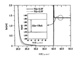
FIG. 11 is a waveform diagram illustrating an output current according to a threshold voltage change of a driving transistor of an organic light emitting display device according to an embodiment of the present invention. FIG. 12 illustrates an organic light emitting device of an organic light emitting display device according to an embodiment of the present invention. It is a wave form diagram which shows the output current by threshold voltage change.
図11に示した波形図は、駆動トランジスタ(Qd)の敷居電圧(Vth)が2.0Vから3.0Vに変化した場合の出力電流(ILD)の変化量を示す。模擬実験はSPICEを利用して行った。模擬実験条件としては、駆動電圧(Vdd)は15V、共通電圧(Vss)は0Vとし、データ電圧(Vdata)は−4.5Vに設定した。このような実験条件下で有機発光素子(LD)に流れる出力電流(ILD)を測定した結果、図11に示したように、出力電流(ILD)は敷居電圧(Vth)が2.0Vである場合に1.394μAであり、敷居電圧(Vth)が3.0Vである場合に1.375μAであった。したがって、駆動トランジスタ(Qd)の敷居電圧(Vth)が1Vだけ高まる場合の電流の変化量は19μAであり、変化前の電流と対比して1.363%が変化した。このような出力電流(ILD)の変動は、従来の2個の薄膜トランジスタを備えた画素での駆動トランジスタの敷居電圧変化による出力電流変動に比べると無視できる程度の数値である。 The waveform diagram shown in FIG. 11 shows the amount of change in the output current (I LD ) when the threshold voltage (Vth) of the drive transistor (Qd) changes from 2.0V to 3.0V. The simulation experiment was performed using SPICE. As simulation conditions, the drive voltage (Vdd) was 15 V, the common voltage (Vss) was 0 V, and the data voltage (V data ) was set to −4.5 V. As a result of measuring the output current (I LD ) flowing through the organic light emitting device (LD) under such experimental conditions, the output current (I LD ) has a threshold voltage (Vth) of 2.0 V as shown in FIG. And 1.375 μA when the threshold voltage is 3.0 V, and 1.375 μA. Therefore, the amount of change in current when the threshold voltage (Vth) of the drive transistor (Qd) is increased by 1 V is 19 μA, which is 1.363% compared with the current before the change. Such fluctuation of the output current (I LD ) is a numerical value that can be ignored as compared with the fluctuation of the output current due to the change of the threshold voltage of the driving transistor in the pixel including the conventional two thin film transistors.
図12に示した波形図は、有機発光素子(LD)の敷居電圧(Vth_LD)が2.8Vから3.3Vに変化した場合の出力電流(ILD)の変化量を示す。上述の実験条件と同一な実験条件下で有機発光素子(LD)に流れる出力電流(ILD)を測定した結果、図12に示したように、出力電流(ILD)は、敷居電圧(Vth_LD)が2.8Vである場合に1.306μAであり、敷居電圧(Vth_LD)が3.3Vである場合に1.291μAであった。したがって、有機発光素子(LD)の敷居電圧(Vth_LD)が0.5V上昇した場合の電流の変化量は15μAであり、劣化前の電流と対比して1.149%が変化した。このような出力電流(ILD)の変動は、従来の2個の薄膜トランジスタを備えた画素での有機発光素子の敷居電圧劣化による出力電流変動に比べると無視できる程度の数値である。
このような模擬実験結果は、駆動トランジスタ(Qd)の敷居電圧(Vth)及び有機発光素子(LD)の敷居電圧(Vth_LD)が劣化しても、本実施例による有機発光表示装置がこれを補償することができるということを示す。
The waveform diagram shown in FIG. 12 shows the amount of change in the output current (I LD ) when the threshold voltage (Vth_ LD ) of the organic light emitting element (LD) is changed from 2.8V to 3.3V. As a result of measuring the output current (I LD ) flowing through the organic light emitting device (LD) under the same experimental conditions as described above, as shown in FIG. 12, the output current (I LD ) is the threshold voltage (Vth_ LD) is 1.306μA if it is 2.8V, the threshold voltage (Vth_ LD) was 1.291μA if it is 3.3V. Therefore, the amount of change in current when the threshold voltage (Vth_ LD) rises 0.5V of the organic light emitting element (LD) is 15 .mu.A, 1.149% is changed in comparison with before degradation of the current. Such fluctuation of the output current (I LD ) is a numerical value that can be ignored as compared with the fluctuation of the output current due to deterioration of the threshold voltage of the organic light emitting element in the pixel having the conventional two thin film transistors.
Such simulation results also threshold voltage (Vth) and the threshold voltage of the organic light emitting element (LD) of the driving transistor (Qd) (Vth_ LD) is deteriorated, the organic light emitting display device according to the present embodiment this Indicates that it can be compensated.
尚、本発明は、上述の実施例に限られるものではない。本発明の技術的範囲から逸脱しない範囲内で多様に変更実施することが可能である。 The present invention is not limited to the above-described embodiments. Various modifications can be made without departing from the technical scope of the present invention.
110 絶縁基板
124 制御端子電極
140 絶縁膜
154 半導体
163、165 抵抗性接触部材
173 入力端子電極
175 出力端子電極
180 保護膜
185 接触孔
190 画素電極
270 共通電極
300 表示板
361 隔壁
370 有機発光層
382 補助電極
400 走査駆動部
500 データ駆動部
600 信号制御部
700 発光駆動部
110 Insulating
Claims (17)
キャパシタと、
制御端子、入力端子、及び出力端子を有し、前記発光素子が発光するように発光素子に駆動電流を供給する駆動トランジスタと、
走査信号に応じて前記駆動トランジスタをダイオード接続させ、データ電圧を前記キャパシタに供給する第1スイッチング部と、
発光信号に応じて駆動電圧を前記駆動トランジスタに供給し、前記キャパシタを前記駆動トランジスタに接続する第2スイッチング部とを各々含む複数の画素を有し、
前記キャパシタは、前記第1スイッチング部を介して前記駆動トランジスタに接続されて、前記データ電圧と前記駆動トランジスタの敷居電圧に依存する制御電圧とを保存し、前記第2スイッチング部を介して前記駆動トランジスタに接続されて前記制御電圧を前記駆動トランジスタに供給することを特徴とする表示装置。 A light emitting element;
A capacitor;
A driving transistor having a control terminal, an input terminal, and an output terminal, and supplying a driving current to the light emitting element so that the light emitting element emits light;
A first switching unit configured to diode-connect the driving transistor according to a scanning signal and supply a data voltage to the capacitor;
A plurality of pixels each including a second switching unit that supplies a driving voltage to the driving transistor according to a light emission signal and connects the capacitor to the driving transistor;
The capacitor is connected to the driving transistor through the first switching unit to store the data voltage and a control voltage depending on a threshold voltage of the driving transistor, and the driving through the second switching unit. A display device connected to a transistor to supply the control voltage to the driving transistor.
前記走査信号に応じて前記キャパシタを前記データ電圧に接続する第2スイッチングトランジスタとを有することを特徴とする請求項1に記載の表示装置。 The first switching unit includes a first switching transistor that connects a control terminal and an input terminal of the driving transistor according to the scanning signal;
The display device according to claim 1, further comprising: a second switching transistor that connects the capacitor to the data voltage in accordance with the scanning signal.
前記発光信号に応じて前記キャパシタと前記駆動トランジスタの出力端子とを接続する第5スイッチングトランジスタとを有することを特徴とする請求項1に記載の表示装置。 The second switching unit includes a fourth switching transistor that connects an input terminal of the driving transistor to the driving voltage according to the light emission signal;
The display device according to claim 1, further comprising a fifth switching transistor that connects the capacitor and an output terminal of the driving transistor in accordance with the light emission signal.
第1電圧に接続されている第1端子、前記発光素子に接続されている第2端子、及び制御端子を有する駆動トランジスタと、
前記駆動トランジスタの第2端子と制御端子との間に接続されているキャパシタと、
走査信号に応答して動作し、前記駆動トランジスタの第1端子と制御端子との間に接続されている第1スイッチング素子と、
前記走査信号に応答して動作し、前記キャパシタとデータ電圧との間に接続されている第2スイッチング素子と、
前記走査信号に応答して動作し、前記駆動トランジスタの第2端子と第2電圧との間に接続されている第3スイッチング素子と、
発光信号に応答して動作し、前記第1電圧と前記駆動トランジスタの第1端子との間に接続されている第4スイッチング素子と、
前記発光信号に応答して動作し、前記キャパシタと前記駆動トランジスタの第2端子との間に接続されている第5スイッチング素子とを有することを特徴とする表示装置。 A light emitting element;
A drive transistor having a first terminal connected to a first voltage, a second terminal connected to the light emitting element, and a control terminal;
A capacitor connected between a second terminal and a control terminal of the drive transistor;
A first switching element that operates in response to a scanning signal and is connected between a first terminal and a control terminal of the driving transistor;
A second switching element operating in response to the scan signal and connected between the capacitor and a data voltage;
A third switching element that operates in response to the scanning signal and is connected between a second terminal of the driving transistor and a second voltage;
A fourth switching element that operates in response to the light emission signal and is connected between the first voltage and the first terminal of the driving transistor;
A display device comprising: a fifth switching element that operates in response to the light emission signal and is connected between the capacitor and a second terminal of the driving transistor.
前記第1区間の間で前記第1乃至第5スイッチング素子がターンオンされており、
前記第2区間の間で前記第1乃至第3スイッチング素子がターンオンされ、前記第4及び第5スイッチング素子がターンオフされており、
前記第3区間の間で前記第1乃至第5スイッチング素子がターンオフされており、
前記第4区間の間で前記第1乃至第3スイッチング素子がターンオフされ、前記第4及び第5スイッチング素子がターンオンされていることを特徴とする請求項10に記載の表示装置。 In the first to fourth sections, which are sequentially sequential, which divide the display operation of the display device,
The first to fifth switching elements are turned on during the first period,
The first to third switching elements are turned on during the second period, and the fourth and fifth switching elements are turned off.
The first to fifth switching elements are turned off during the third period,
11. The display device of claim 10, wherein the first to third switching elements are turned off and the fourth and fifth switching elements are turned on during the fourth period.
前記駆動トランジスタの制御端子と第1端子とを接続する段階と、
前記駆動トランジスタの第2端子を共通電圧に接続する段階と、
前記キャパシタをデータ電圧に接続する段階と、
前記キャパシタを前記駆動トランジスタの制御端子と第2端子との間に接続する段階と、
前記駆動トランジスタの第1端子を駆動電圧に接続する段階とを有することを特徴とする表示装置の駆動方法。 A display device comprising: a drive transistor having a control terminal and first and second terminals; a light emitting element connected to the second terminal of the drive transistor; and a capacitor connected to the control terminal of the drive transistor. In the driving method,
Connecting the control terminal and the first terminal of the driving transistor;
Connecting the second terminal of the driving transistor to a common voltage;
Connecting the capacitor to a data voltage;
Connecting the capacitor between a control terminal and a second terminal of the driving transistor;
Connecting the first terminal of the driving transistor to a driving voltage.
前記キャパシタに第1電圧及びデータ電圧を印加して充電する段階と、
前記キャパシタに充電された電圧を前記駆動トランジスタを通して第2電圧側に放電する段階と、
前記キャパシタの放電後の電圧を前記駆動トランジスタに印加して前記駆動トランジスタをターンオンさせる段階と、
前記駆動トランジスタを通して前記発光素子に駆動電流を供給して発光させる段階とを有することを特徴とする表示装置の駆動方法。 In a driving method of a display device including a light emitting element, a driving transistor connected to the light emitting element, and a capacitor connected to the driving transistor and the light emitting element,
Charging the capacitor by applying a first voltage and a data voltage;
Discharging the voltage charged in the capacitor to the second voltage side through the driving transistor;
Applying a voltage after discharging of the capacitor to the driving transistor to turn on the driving transistor;
And a step of supplying a driving current to the light emitting element through the driving transistor to cause the light emitting element to emit light.
Applications Claiming Priority (2)
| Application Number | Priority Date | Filing Date | Title |
|---|---|---|---|
| KR10-2004-0093210 | 2004-11-15 | ||
| KR1020040093210A KR20060054603A (en) | 2004-11-15 | 2004-11-15 | Display device and driving method thereof |
Publications (2)
| Publication Number | Publication Date |
|---|---|
| JP2006146219A true JP2006146219A (en) | 2006-06-08 |
| JP5080733B2 JP5080733B2 (en) | 2012-11-21 |
Family
ID=36385570
Family Applications (1)
| Application Number | Title | Priority Date | Filing Date |
|---|---|---|---|
| JP2005330899A Expired - Lifetime JP5080733B2 (en) | 2004-11-15 | 2005-11-15 | Display device and driving method thereof |
Country Status (5)
| Country | Link |
|---|---|
| US (1) | US8619006B2 (en) |
| JP (1) | JP5080733B2 (en) |
| KR (1) | KR20060054603A (en) |
| CN (1) | CN1776797B (en) |
| TW (1) | TWI423196B (en) |
Cited By (8)
| Publication number | Priority date | Publication date | Assignee | Title |
|---|---|---|---|---|
| JP2007156420A (en) * | 2005-12-02 | 2007-06-21 | Samsung Electronics Co Ltd | Display device and driving method thereof |
| JP2008052279A (en) * | 2006-08-24 | 2008-03-06 | Toppoly Optoelectronics Corp | Image display system |
| JP2008122906A (en) * | 2006-11-14 | 2008-05-29 | Samsung Sdi Co Ltd | Pixel, organic electroluminescent display device, and driving method of organic electroluminescent display device |
| JP2008225432A (en) * | 2007-03-14 | 2008-09-25 | Samsung Sdi Co Ltd | Pixel, organic electroluminescence display device using the same, and driving method thereof |
| JP2008262144A (en) * | 2007-04-10 | 2008-10-30 | Samsung Sdi Co Ltd | Pixel, organic electroluminescence display device using the same, and driving method thereof |
| JP2009265328A (en) * | 2008-04-24 | 2009-11-12 | Toshiba Mobile Display Co Ltd | El display device |
| WO2011004646A1 (en) * | 2009-07-10 | 2011-01-13 | シャープ株式会社 | Display device |
| US8194012B2 (en) | 2008-03-10 | 2012-06-05 | Samsung Mobile Display Co.,Ltd. | Pixel and organic light emitting display using the same |
Families Citing this family (60)
| Publication number | Priority date | Publication date | Assignee | Title |
|---|---|---|---|---|
| US10013907B2 (en) | 2004-12-15 | 2018-07-03 | Ignis Innovation Inc. | Method and system for programming, calibrating and/or compensating, and driving an LED display |
| US9799246B2 (en) | 2011-05-20 | 2017-10-24 | Ignis Innovation Inc. | System and methods for extraction of threshold and mobility parameters in AMOLED displays |
| US8576217B2 (en) | 2011-05-20 | 2013-11-05 | Ignis Innovation Inc. | System and methods for extraction of threshold and mobility parameters in AMOLED displays |
| KR101160830B1 (en) * | 2005-04-21 | 2012-06-29 | 삼성전자주식회사 | Display device and driving method thereof |
| CN102663977B (en) | 2005-06-08 | 2015-11-18 | 伊格尼斯创新有限公司 | For driving the method and system of light emitting device display |
| EP1793366A3 (en) | 2005-12-02 | 2009-11-04 | Semiconductor Energy Laboratory Co., Ltd. | Semiconductor device, display device, and electronic device |
| JP5397219B2 (en) | 2006-04-19 | 2014-01-22 | イグニス・イノベーション・インコーポレイテッド | Stable drive scheme for active matrix display |
| CA2556961A1 (en) * | 2006-08-15 | 2008-02-15 | Ignis Innovation Inc. | Oled compensation technique based on oled capacitance |
| CN100437708C (en) * | 2006-09-22 | 2008-11-26 | 北京交通大学 | Pixel drive circuit of active organic electroluminescent display device |
| KR101373736B1 (en) | 2006-12-27 | 2014-03-14 | 삼성디스플레이 주식회사 | Display device and driving method thereof |
| JP2008170756A (en) * | 2007-01-12 | 2008-07-24 | Sony Corp | Display device |
| KR100873074B1 (en) | 2007-03-02 | 2008-12-09 | 삼성모바일디스플레이주식회사 | Pixel and organic light emitting display device using same and driving method thereof |
| KR101288595B1 (en) * | 2007-03-07 | 2013-07-22 | 엘지디스플레이 주식회사 | Organic Light Emitting Diode Display And Driving Method Thereof |
| TWI378428B (en) * | 2007-07-04 | 2012-12-01 | Tpo Displays Corp | Control method, display panel, and electronic system utilizing the same |
| KR100902221B1 (en) * | 2008-01-28 | 2009-06-11 | 삼성모바일디스플레이주식회사 | Pixel and organic light emitting display device using same |
| KR100911981B1 (en) | 2008-03-04 | 2009-08-13 | 삼성모바일디스플레이주식회사 | Pixel and organic light emitting display device using same |
| KR101008438B1 (en) | 2008-11-26 | 2011-01-14 | 삼성모바일디스플레이주식회사 | Pixel and organic light emitting display device using same |
| KR101056317B1 (en) | 2009-04-02 | 2011-08-11 | 삼성모바일디스플레이주식회사 | Pixel and organic light emitting display device using same |
| US10319307B2 (en) | 2009-06-16 | 2019-06-11 | Ignis Innovation Inc. | Display system with compensation techniques and/or shared level resources |
| US9384698B2 (en) | 2009-11-30 | 2016-07-05 | Ignis Innovation Inc. | System and methods for aging compensation in AMOLED displays |
| US9311859B2 (en) | 2009-11-30 | 2016-04-12 | Ignis Innovation Inc. | Resetting cycle for aging compensation in AMOLED displays |
| KR20110082931A (en) * | 2010-01-12 | 2011-07-20 | 삼성전기주식회사 | Compensation device for degradation of an active organic light emitting display |
| US10089921B2 (en) | 2010-02-04 | 2018-10-02 | Ignis Innovation Inc. | System and methods for extracting correlation curves for an organic light emitting device |
| US9881532B2 (en) | 2010-02-04 | 2018-01-30 | Ignis Innovation Inc. | System and method for extracting correlation curves for an organic light emitting device |
| CA2692097A1 (en) | 2010-02-04 | 2011-08-04 | Ignis Innovation Inc. | Extracting correlation curves for light emitting device |
| US20140313111A1 (en) | 2010-02-04 | 2014-10-23 | Ignis Innovation Inc. | System and methods for extracting correlation curves for an organic light emitting device |
| JP2012098317A (en) * | 2010-10-29 | 2012-05-24 | Hitachi Displays Ltd | Image display and method for driving the same |
| US9530349B2 (en) | 2011-05-20 | 2016-12-27 | Ignis Innovations Inc. | Charged-based compensation and parameter extraction in AMOLED displays |
| US9466240B2 (en) | 2011-05-26 | 2016-10-11 | Ignis Innovation Inc. | Adaptive feedback system for compensating for aging pixel areas with enhanced estimation speed |
| US9773439B2 (en) | 2011-05-27 | 2017-09-26 | Ignis Innovation Inc. | Systems and methods for aging compensation in AMOLED displays |
| US12176356B2 (en) | 2011-10-18 | 2024-12-24 | Semiconductor Energy Laboratory Co., Ltd. | Semiconductor device including transistor and light-emitting element |
| KR20190033094A (en) | 2011-10-18 | 2019-03-28 | 가부시키가이샤 한도오따이 에네루기 켄큐쇼 | Method for driving semiconductor device |
| US10089924B2 (en) | 2011-11-29 | 2018-10-02 | Ignis Innovation Inc. | Structural and low-frequency non-uniformity compensation |
| US9324268B2 (en) | 2013-03-15 | 2016-04-26 | Ignis Innovation Inc. | Amoled displays with multiple readout circuits |
| US8937632B2 (en) | 2012-02-03 | 2015-01-20 | Ignis Innovation Inc. | Driving system for active-matrix displays |
| US8922544B2 (en) | 2012-05-23 | 2014-12-30 | Ignis Innovation Inc. | Display systems with compensation for line propagation delay |
| US9320111B2 (en) * | 2012-05-31 | 2016-04-19 | Semiconductor Energy Laboratory Co., Ltd. | Light-emitting device |
| CN102789761B (en) * | 2012-08-06 | 2014-12-10 | 京东方科技集团股份有限公司 | Pixel circuit, driving method thereof and organic light emitting display |
| EP3043338A1 (en) | 2013-03-14 | 2016-07-13 | Ignis Innovation Inc. | Re-interpolation with edge detection for extracting an aging pattern for amoled displays |
| US9761170B2 (en) | 2013-12-06 | 2017-09-12 | Ignis Innovation Inc. | Correction for localized phenomena in an image array |
| US9502653B2 (en) | 2013-12-25 | 2016-11-22 | Ignis Innovation Inc. | Electrode contacts |
| CN103927982B (en) | 2014-03-24 | 2016-08-17 | 京东方科技集团股份有限公司 | Image element circuit and driving method, display device |
| CN103985360B (en) * | 2014-05-04 | 2016-04-27 | 深圳市华星光电技术有限公司 | The driving circuit of display panel and liquid crystal indicator |
| CN104167168B (en) * | 2014-06-23 | 2016-09-07 | 京东方科技集团股份有限公司 | Image element circuit and driving method thereof and display device |
| CN104134426B (en) * | 2014-07-07 | 2017-02-15 | 京东方科技集团股份有限公司 | Pixel structure and driving method thereof, and display device |
| CA2879462A1 (en) | 2015-01-23 | 2016-07-23 | Ignis Innovation Inc. | Compensation for color variation in emissive devices |
| CN104715726A (en) * | 2015-04-07 | 2015-06-17 | 合肥鑫晟光电科技有限公司 | Pixel driving circuit, pixel driving method and display device |
| CA2889870A1 (en) | 2015-05-04 | 2016-11-04 | Ignis Innovation Inc. | Optical feedback system |
| CA2892714A1 (en) | 2015-05-27 | 2016-11-27 | Ignis Innovation Inc | Memory bandwidth reduction in compensation system |
| CA2900170A1 (en) | 2015-08-07 | 2017-02-07 | Gholamreza Chaji | Calibration of pixel based on improved reference values |
| KR102389343B1 (en) * | 2015-08-27 | 2022-04-25 | 삼성디스플레이 주식회사 | Pixel, organic light emitting display device including the pixel and driving method of the pixel |
| CN105118438B (en) * | 2015-09-21 | 2017-07-25 | 京东方科技集团股份有限公司 | Pixel driving circuit, method, pixel circuit and display device |
| CN105427795A (en) * | 2016-01-11 | 2016-03-23 | 京东方科技集团股份有限公司 | Pixel driving circuit and method, pixel structure, and display device |
| KR102456297B1 (en) | 2016-04-15 | 2022-10-20 | 삼성디스플레이 주식회사 | Pixel circuit and method of driving the same |
| KR102566551B1 (en) * | 2016-12-05 | 2023-08-14 | 삼성디스플레이주식회사 | Display device and method for driving the same |
| CN111028780A (en) * | 2019-12-03 | 2020-04-17 | 武汉华星光电半导体显示技术有限公司 | Pixel compensation circuit of AMOLED |
| CN113539171A (en) * | 2021-07-27 | 2021-10-22 | 深圳市华星光电半导体显示技术有限公司 | Display pixel circuit, display pixel circuit driving method and display panel |
| KR20230093997A (en) * | 2021-12-20 | 2023-06-27 | 엘지디스플레이 주식회사 | Display Panel And Display Device Including The Same |
| TWI903131B (en) * | 2022-03-30 | 2025-11-01 | 群創光電股份有限公司 | Electronic device and setting method for electronic device |
| CN116844500B (en) * | 2023-07-10 | 2025-08-22 | 京东方科技集团股份有限公司 | Display control method and device, electronic device, and display device |
Citations (4)
| Publication number | Priority date | Publication date | Assignee | Title |
|---|---|---|---|---|
| JP2004246204A (en) * | 2003-02-14 | 2004-09-02 | Sony Corp | Pixel circuit, display device, and driving method of pixel circuit |
| JP2005157244A (en) * | 2003-11-27 | 2005-06-16 | Samsung Sdi Co Ltd | Light emitting display device, display panel and driving method thereof |
| JP2005157308A (en) * | 2003-11-24 | 2005-06-16 | Samsung Sdi Co Ltd | Light emitting display device, display panel, and driving method of light emitting display device |
| JP2005326828A (en) * | 2004-04-12 | 2005-11-24 | Sanyo Electric Co Ltd | Organic EL pixel circuit |
Family Cites Families (17)
| Publication number | Priority date | Publication date | Assignee | Title |
|---|---|---|---|---|
| EP1130565A4 (en) * | 1999-07-14 | 2006-10-04 | Sony Corp | ATTACK CIRCUIT AND DISPLAY INCLUDING THE SAME, PIXEL CIRCUIT, AND ATTACK METHOD |
| KR20020027957A (en) | 2000-10-06 | 2002-04-15 | 구자홍 | drive circuit for current driving of active matrix formula |
| JP3593982B2 (en) * | 2001-01-15 | 2004-11-24 | ソニー株式会社 | Active matrix type display device, active matrix type organic electroluminescence display device, and driving method thereof |
| JP3951687B2 (en) | 2001-08-02 | 2007-08-01 | セイコーエプソン株式会社 | Driving data lines used to control unit circuits |
| CN101257743B (en) | 2001-08-29 | 2011-05-25 | 株式会社半导体能源研究所 | Light emitting device and driving method of the light emitting device |
| KR100940342B1 (en) * | 2001-11-13 | 2010-02-04 | 가부시키가이샤 한도오따이 에네루기 켄큐쇼 | Display device and driving method |
| KR100452114B1 (en) | 2002-04-15 | 2004-10-12 | 한국과학기술원 | Pixel circuit and Organic Light Eitting Dode display using the same |
| KR100445435B1 (en) | 2002-07-23 | 2004-08-21 | 삼성에스디아이 주식회사 | Display device of organic electro luminescent and driving method there of |
| JP3832415B2 (en) * | 2002-10-11 | 2006-10-11 | ソニー株式会社 | Active matrix display device |
| KR100490622B1 (en) | 2003-01-21 | 2005-05-17 | 삼성에스디아이 주식회사 | Organic electroluminescent display and driving method and pixel circuit thereof |
| KR100497247B1 (en) | 2003-04-01 | 2005-06-23 | 삼성에스디아이 주식회사 | Light emitting display device and display panel and driving method thereof |
| JP2005099715A (en) * | 2003-08-29 | 2005-04-14 | Seiko Epson Corp | Electronic circuit driving method, electronic circuit, electronic device, electro-optical device, electronic apparatus, and electronic device driving method |
| US7193588B2 (en) * | 2003-09-29 | 2007-03-20 | Wintek Corporation | Active matrix organic electroluminescence display driving circuit |
| US6937215B2 (en) * | 2003-11-03 | 2005-08-30 | Wintek Corporation | Pixel driving circuit of an organic light emitting diode display panel |
| JP5105694B2 (en) * | 2003-12-24 | 2012-12-26 | 株式会社半導体エネルギー研究所 | Display device and electronic device |
| US7173585B2 (en) * | 2004-03-10 | 2007-02-06 | Wintek Corporation | Active matrix display driving circuit |
| KR100595101B1 (en) | 2004-11-10 | 2006-07-03 | 삼성에스디아이 주식회사 | Data integrated circuit and light emitting display device using the same |
-
2004
- 2004-11-15 KR KR1020040093210A patent/KR20060054603A/en not_active Ceased
-
2005
- 2005-10-19 TW TW094136507A patent/TWI423196B/en not_active IP Right Cessation
- 2005-11-14 US US11/274,913 patent/US8619006B2/en active Active
- 2005-11-15 JP JP2005330899A patent/JP5080733B2/en not_active Expired - Lifetime
- 2005-11-15 CN CN2005101247962A patent/CN1776797B/en not_active Expired - Lifetime
Patent Citations (4)
| Publication number | Priority date | Publication date | Assignee | Title |
|---|---|---|---|---|
| JP2004246204A (en) * | 2003-02-14 | 2004-09-02 | Sony Corp | Pixel circuit, display device, and driving method of pixel circuit |
| JP2005157308A (en) * | 2003-11-24 | 2005-06-16 | Samsung Sdi Co Ltd | Light emitting display device, display panel, and driving method of light emitting display device |
| JP2005157244A (en) * | 2003-11-27 | 2005-06-16 | Samsung Sdi Co Ltd | Light emitting display device, display panel and driving method thereof |
| JP2005326828A (en) * | 2004-04-12 | 2005-11-24 | Sanyo Electric Co Ltd | Organic EL pixel circuit |
Cited By (13)
| Publication number | Priority date | Publication date | Assignee | Title |
|---|---|---|---|---|
| JP2007156420A (en) * | 2005-12-02 | 2007-06-21 | Samsung Electronics Co Ltd | Display device and driving method thereof |
| JP2008052279A (en) * | 2006-08-24 | 2008-03-06 | Toppoly Optoelectronics Corp | Image display system |
| US8054258B2 (en) | 2006-11-14 | 2011-11-08 | Samsung Mobile Display Co., Ltd. | Pixel, organic light emitting display device and driving method thereof |
| JP2008122906A (en) * | 2006-11-14 | 2008-05-29 | Samsung Sdi Co Ltd | Pixel, organic electroluminescent display device, and driving method of organic electroluminescent display device |
| JP2008225432A (en) * | 2007-03-14 | 2008-09-25 | Samsung Sdi Co Ltd | Pixel, organic electroluminescence display device using the same, and driving method thereof |
| US8111219B2 (en) | 2007-03-14 | 2012-02-07 | Samsung Mobile Display Co., Ltd. | Pixel, organic light emitting display using the same, and associated methods |
| US8149186B2 (en) | 2007-04-10 | 2012-04-03 | Samsung Mobile Display Co., Ltd. | Pixel, organic light emitting display using the same, and associated methods |
| JP2008262144A (en) * | 2007-04-10 | 2008-10-30 | Samsung Sdi Co Ltd | Pixel, organic electroluminescence display device using the same, and driving method thereof |
| US8194012B2 (en) | 2008-03-10 | 2012-06-05 | Samsung Mobile Display Co.,Ltd. | Pixel and organic light emitting display using the same |
| JP2009265328A (en) * | 2008-04-24 | 2009-11-12 | Toshiba Mobile Display Co Ltd | El display device |
| WO2011004646A1 (en) * | 2009-07-10 | 2011-01-13 | シャープ株式会社 | Display device |
| JP5214030B2 (en) * | 2009-07-10 | 2013-06-19 | シャープ株式会社 | Display device |
| US8605077B2 (en) | 2009-07-10 | 2013-12-10 | Sharp Kabushiki Kaisha | Display device |
Also Published As
| Publication number | Publication date |
|---|---|
| CN1776797B (en) | 2010-05-05 |
| US20060103324A1 (en) | 2006-05-18 |
| KR20060054603A (en) | 2006-05-23 |
| TWI423196B (en) | 2014-01-11 |
| CN1776797A (en) | 2006-05-24 |
| US8619006B2 (en) | 2013-12-31 |
| JP5080733B2 (en) | 2012-11-21 |
| TW200617830A (en) | 2006-06-01 |
Similar Documents
| Publication | Publication Date | Title |
|---|---|---|
| JP5080733B2 (en) | Display device and driving method thereof | |
| JP4963013B2 (en) | Display device | |
| JP5078236B2 (en) | Display device and driving method thereof | |
| KR101152120B1 (en) | Display device and driving method thereof | |
| EP2674932B1 (en) | Organic light emitting diode display with lighting test circuit | |
| US7358938B2 (en) | Circuit and method for driving pixel of organic electroluminescent display | |
| CN100365689C (en) | Image display device and driving method thereof | |
| KR100497247B1 (en) | Light emitting display device and display panel and driving method thereof | |
| KR101209055B1 (en) | Display device and driving method thereof | |
| US20080001857A1 (en) | Organic light-emitting diode display device and driving method thereof | |
| KR101058107B1 (en) | Pixel circuit and organic light emitting display device using the same | |
| KR100599724B1 (en) | Display panel, light emitting display device using same and driving method thereof | |
| JP2006221172A (en) | Display device and driving method thereof | |
| KR20050041665A (en) | Image display apparatus and driving method thereof | |
| KR101495342B1 (en) | Organic Light Emitting Diode Display | |
| JP2006195477A (en) | Display device and driving method thereof | |
| KR20060083101A (en) | Display device and driving method thereof | |
| JP2006243740A (en) | Display device and driving method thereof | |
| KR100515307B1 (en) | Image display apparatus, and driving method thereof | |
| KR101240658B1 (en) | Display device and driving method thereof | |
| KR100741979B1 (en) | Pixel Circuit of Organic Electroluminescent Display | |
| KR100560453B1 (en) | Gate driving circuit of light emitting display device |
Legal Events
| Date | Code | Title | Description |
|---|---|---|---|
| A621 | Written request for application examination |
Free format text: JAPANESE INTERMEDIATE CODE: A621 Effective date: 20080911 |
|
| A977 | Report on retrieval |
Free format text: JAPANESE INTERMEDIATE CODE: A971007 Effective date: 20110519 |
|
| A131 | Notification of reasons for refusal |
Free format text: JAPANESE INTERMEDIATE CODE: A131 Effective date: 20110531 |
|
| A521 | Request for written amendment filed |
Free format text: JAPANESE INTERMEDIATE CODE: A523 Effective date: 20110831 |
|
| A02 | Decision of refusal |
Free format text: JAPANESE INTERMEDIATE CODE: A02 Effective date: 20110927 |
|
| A521 | Request for written amendment filed |
Free format text: JAPANESE INTERMEDIATE CODE: A523 Effective date: 20120125 |
|
| A911 | Transfer to examiner for re-examination before appeal (zenchi) |
Free format text: JAPANESE INTERMEDIATE CODE: A911 Effective date: 20120216 |
|
| A131 | Notification of reasons for refusal |
Free format text: JAPANESE INTERMEDIATE CODE: A131 Effective date: 20120508 |
|
| A521 | Request for written amendment filed |
Free format text: JAPANESE INTERMEDIATE CODE: A523 Effective date: 20120806 |
|
| TRDD | Decision of grant or rejection written | ||
| A01 | Written decision to grant a patent or to grant a registration (utility model) |
Free format text: JAPANESE INTERMEDIATE CODE: A01 Effective date: 20120828 |
|
| A01 | Written decision to grant a patent or to grant a registration (utility model) |
Free format text: JAPANESE INTERMEDIATE CODE: A01 |
|
| A61 | First payment of annual fees (during grant procedure) |
Free format text: JAPANESE INTERMEDIATE CODE: A61 Effective date: 20120831 |
|
| FPAY | Renewal fee payment (event date is renewal date of database) |
Free format text: PAYMENT UNTIL: 20150907 Year of fee payment: 3 |
|
| R150 | Certificate of patent or registration of utility model |
Ref document number: 5080733 Country of ref document: JP Free format text: JAPANESE INTERMEDIATE CODE: R150 Free format text: JAPANESE INTERMEDIATE CODE: R150 |
|
| FPAY | Renewal fee payment (event date is renewal date of database) |
Free format text: PAYMENT UNTIL: 20150907 Year of fee payment: 3 |
|
| S111 | Request for change of ownership or part of ownership |
Free format text: JAPANESE INTERMEDIATE CODE: R313115 |
|
| S631 | Written request for registration of reclamation of domicile |
Free format text: JAPANESE INTERMEDIATE CODE: R313631 |
|
| FPAY | Renewal fee payment (event date is renewal date of database) |
Free format text: PAYMENT UNTIL: 20150907 Year of fee payment: 3 |
|
| R371 | Transfer withdrawn |
Free format text: JAPANESE INTERMEDIATE CODE: R371 |
|
| FPAY | Renewal fee payment (event date is renewal date of database) |
Free format text: PAYMENT UNTIL: 20150907 Year of fee payment: 3 |
|
| S111 | Request for change of ownership or part of ownership |
Free format text: JAPANESE INTERMEDIATE CODE: R313115 |
|
| S631 | Written request for registration of reclamation of domicile |
Free format text: JAPANESE INTERMEDIATE CODE: R313631 |
|
| R350 | Written notification of registration of transfer |
Free format text: JAPANESE INTERMEDIATE CODE: R350 |
|
| R250 | Receipt of annual fees |
Free format text: JAPANESE INTERMEDIATE CODE: R250 |
|
| R250 | Receipt of annual fees |
Free format text: JAPANESE INTERMEDIATE CODE: R250 |
|
| R250 | Receipt of annual fees |
Free format text: JAPANESE INTERMEDIATE CODE: R250 |
|
| R250 | Receipt of annual fees |
Free format text: JAPANESE INTERMEDIATE CODE: R250 |
|
| R250 | Receipt of annual fees |
Free format text: JAPANESE INTERMEDIATE CODE: R250 |
|
| R250 | Receipt of annual fees |
Free format text: JAPANESE INTERMEDIATE CODE: R250 |
|
| R250 | Receipt of annual fees |
Free format text: JAPANESE INTERMEDIATE CODE: R250 |
|
| R250 | Receipt of annual fees |
Free format text: JAPANESE INTERMEDIATE CODE: R250 |
|
| R250 | Receipt of annual fees |
Free format text: JAPANESE INTERMEDIATE CODE: R250 |
|
| R250 | Receipt of annual fees |
Free format text: JAPANESE INTERMEDIATE CODE: R250 |
|
| R250 | Receipt of annual fees |
Free format text: JAPANESE INTERMEDIATE CODE: R250 |