JP2005509752A - Ion plasma deposition system - Google Patents
Ion plasma deposition system Download PDFInfo
- Publication number
- JP2005509752A JP2005509752A JP2003545857A JP2003545857A JP2005509752A JP 2005509752 A JP2005509752 A JP 2005509752A JP 2003545857 A JP2003545857 A JP 2003545857A JP 2003545857 A JP2003545857 A JP 2003545857A JP 2005509752 A JP2005509752 A JP 2005509752A
- Authority
- JP
- Japan
- Prior art keywords
- anode
- cathode
- substrate
- vacuum chamber
- particles
- Prior art date
- Legal status (The legal status is an assumption and is not a legal conclusion. Google has not performed a legal analysis and makes no representation as to the accuracy of the status listed.)
- Pending
Links
- 230000008021 deposition Effects 0.000 title claims description 23
- 239000000758 substrate Substances 0.000 claims abstract description 85
- 239000002245 particle Substances 0.000 claims abstract description 73
- 239000000446 fuel Substances 0.000 claims abstract description 49
- 238000000151 deposition Methods 0.000 claims abstract description 39
- 238000000034 method Methods 0.000 claims abstract description 38
- 230000005672 electromagnetic field Effects 0.000 claims abstract description 29
- 239000003054 catalyst Substances 0.000 claims abstract description 23
- 239000010409 thin film Substances 0.000 claims abstract description 15
- 239000013077 target material Substances 0.000 claims abstract description 11
- 238000010891 electric arc Methods 0.000 claims abstract description 6
- 239000000463 material Substances 0.000 claims description 39
- 239000007789 gas Substances 0.000 claims description 27
- 229910052751 metal Inorganic materials 0.000 claims description 27
- 239000002184 metal Substances 0.000 claims description 27
- OKTJSMMVPCPJKN-UHFFFAOYSA-N Carbon Chemical compound [C] OKTJSMMVPCPJKN-UHFFFAOYSA-N 0.000 claims description 24
- 229910052799 carbon Inorganic materials 0.000 claims description 24
- 238000004519 manufacturing process Methods 0.000 claims description 15
- 230000007935 neutral effect Effects 0.000 claims description 13
- 239000007787 solid Substances 0.000 claims description 13
- 238000007740 vapor deposition Methods 0.000 claims description 6
- 238000001704 evaporation Methods 0.000 claims description 5
- 229920006254 polymer film Polymers 0.000 claims description 4
- 239000012495 reaction gas Substances 0.000 claims description 4
- 239000007770 graphite material Substances 0.000 claims description 2
- 239000011859 microparticle Substances 0.000 claims description 2
- 239000007769 metal material Substances 0.000 claims 1
- 239000012528 membrane Substances 0.000 abstract description 15
- 229920000642 polymer Polymers 0.000 abstract description 7
- 238000000541 cathodic arc deposition Methods 0.000 abstract description 2
- 210000004027 cell Anatomy 0.000 description 41
- 150000002500 ions Chemical class 0.000 description 12
- 230000003197 catalytic effect Effects 0.000 description 11
- 238000012216 screening Methods 0.000 description 11
- 239000010406 cathode material Substances 0.000 description 10
- BASFCYQUMIYNBI-UHFFFAOYSA-N platinum Chemical compound [Pt] BASFCYQUMIYNBI-UHFFFAOYSA-N 0.000 description 10
- XKRFYHLGVUSROY-UHFFFAOYSA-N Argon Chemical compound [Ar] XKRFYHLGVUSROY-UHFFFAOYSA-N 0.000 description 8
- 229920000106 Liquid crystal polymer Polymers 0.000 description 7
- 239000004977 Liquid-crystal polymers (LCPs) Substances 0.000 description 7
- 239000004020 conductor Substances 0.000 description 6
- 230000008569 process Effects 0.000 description 6
- 239000003570 air Substances 0.000 description 5
- 239000011248 coating agent Substances 0.000 description 5
- 238000000576 coating method Methods 0.000 description 5
- PCHJSUWPFVWCPO-UHFFFAOYSA-N gold Chemical compound [Au] PCHJSUWPFVWCPO-UHFFFAOYSA-N 0.000 description 5
- 229910052737 gold Inorganic materials 0.000 description 5
- 239000010931 gold Substances 0.000 description 5
- 238000005304 joining Methods 0.000 description 5
- 150000002739 metals Chemical class 0.000 description 5
- 230000009257 reactivity Effects 0.000 description 5
- IJGRMHOSHXDMSA-UHFFFAOYSA-N Atomic nitrogen Chemical compound N#N IJGRMHOSHXDMSA-UHFFFAOYSA-N 0.000 description 4
- RYGMFSIKBFXOCR-UHFFFAOYSA-N Copper Chemical compound [Cu] RYGMFSIKBFXOCR-UHFFFAOYSA-N 0.000 description 4
- 229910045601 alloy Inorganic materials 0.000 description 4
- 239000000956 alloy Substances 0.000 description 4
- 229910052786 argon Inorganic materials 0.000 description 4
- 239000000919 ceramic Substances 0.000 description 4
- 229910052802 copper Inorganic materials 0.000 description 4
- 239000010949 copper Substances 0.000 description 4
- 239000002105 nanoparticle Substances 0.000 description 4
- 239000004033 plastic Substances 0.000 description 4
- 229920003023 plastic Polymers 0.000 description 4
- 229910052697 platinum Inorganic materials 0.000 description 4
- XLYOFNOQVPJJNP-UHFFFAOYSA-N water Chemical compound O XLYOFNOQVPJJNP-UHFFFAOYSA-N 0.000 description 4
- 230000008901 benefit Effects 0.000 description 3
- 230000015572 biosynthetic process Effects 0.000 description 3
- 238000005137 deposition process Methods 0.000 description 3
- 238000010586 diagram Methods 0.000 description 3
- -1 for example Substances 0.000 description 3
- 230000006872 improvement Effects 0.000 description 3
- LYCAIKOWRPUZTN-UHFFFAOYSA-N Ethylene glycol Chemical compound OCCO LYCAIKOWRPUZTN-UHFFFAOYSA-N 0.000 description 2
- PXHVJJICTQNCMI-UHFFFAOYSA-N Nickel Chemical compound [Ni] PXHVJJICTQNCMI-UHFFFAOYSA-N 0.000 description 2
- 239000005062 Polybutadiene Substances 0.000 description 2
- 239000010405 anode material Substances 0.000 description 2
- 238000013459 approach Methods 0.000 description 2
- QVGXLLKOCUKJST-UHFFFAOYSA-N atomic oxygen Chemical compound [O] QVGXLLKOCUKJST-UHFFFAOYSA-N 0.000 description 2
- 150000001721 carbon Chemical class 0.000 description 2
- 238000007796 conventional method Methods 0.000 description 2
- 238000001816 cooling Methods 0.000 description 2
- 239000012809 cooling fluid Substances 0.000 description 2
- 238000005260 corrosion Methods 0.000 description 2
- 230000007797 corrosion Effects 0.000 description 2
- 239000006185 dispersion Substances 0.000 description 2
- 230000009977 dual effect Effects 0.000 description 2
- 230000000694 effects Effects 0.000 description 2
- 239000010408 film Substances 0.000 description 2
- 238000001914 filtration Methods 0.000 description 2
- 239000011261 inert gas Substances 0.000 description 2
- 229920000554 ionomer Polymers 0.000 description 2
- VNWKTOKETHGBQD-UHFFFAOYSA-N methane Chemical compound C VNWKTOKETHGBQD-UHFFFAOYSA-N 0.000 description 2
- 238000012986 modification Methods 0.000 description 2
- 230000004048 modification Effects 0.000 description 2
- 239000002086 nanomaterial Substances 0.000 description 2
- 150000004767 nitrides Chemical class 0.000 description 2
- 229910052757 nitrogen Inorganic materials 0.000 description 2
- 229910052760 oxygen Inorganic materials 0.000 description 2
- 239000001301 oxygen Substances 0.000 description 2
- 229920002857 polybutadiene Polymers 0.000 description 2
- 229920005597 polymer membrane Polymers 0.000 description 2
- 238000006116 polymerization reaction Methods 0.000 description 2
- 229910052707 ruthenium Inorganic materials 0.000 description 2
- 239000004065 semiconductor Substances 0.000 description 2
- 238000005019 vapor deposition process Methods 0.000 description 2
- LSNNMFCWUKXFEE-UHFFFAOYSA-M Bisulfite Chemical compound OS([O-])=O LSNNMFCWUKXFEE-UHFFFAOYSA-M 0.000 description 1
- 239000004215 Carbon black (E152) Substances 0.000 description 1
- VYZAMTAEIAYCRO-UHFFFAOYSA-N Chromium Chemical compound [Cr] VYZAMTAEIAYCRO-UHFFFAOYSA-N 0.000 description 1
- 239000004695 Polyether sulfone Substances 0.000 description 1
- 239000004698 Polyethylene Substances 0.000 description 1
- KJTLSVCANCCWHF-UHFFFAOYSA-N Ruthenium Chemical compound [Ru] KJTLSVCANCCWHF-UHFFFAOYSA-N 0.000 description 1
- BQCADISMDOOEFD-UHFFFAOYSA-N Silver Chemical compound [Ag] BQCADISMDOOEFD-UHFFFAOYSA-N 0.000 description 1
- RTAQQCXQSZGOHL-UHFFFAOYSA-N Titanium Chemical compound [Ti] RTAQQCXQSZGOHL-UHFFFAOYSA-N 0.000 description 1
- QCWXUUIWCKQGHC-UHFFFAOYSA-N Zirconium Chemical compound [Zr] QCWXUUIWCKQGHC-UHFFFAOYSA-N 0.000 description 1
- 238000005299 abrasion Methods 0.000 description 1
- 229910052782 aluminium Inorganic materials 0.000 description 1
- XAGFODPZIPBFFR-UHFFFAOYSA-N aluminium Chemical compound [Al] XAGFODPZIPBFFR-UHFFFAOYSA-N 0.000 description 1
- 238000005452 bending Methods 0.000 description 1
- 238000005513 bias potential Methods 0.000 description 1
- 238000005219 brazing Methods 0.000 description 1
- 239000011852 carbon nanoparticle Substances 0.000 description 1
- 239000002717 carbon nanostructure Substances 0.000 description 1
- 239000002041 carbon nanotube Substances 0.000 description 1
- 229910021393 carbon nanotube Inorganic materials 0.000 description 1
- 239000003575 carbonaceous material Substances 0.000 description 1
- 230000015556 catabolic process Effects 0.000 description 1
- 210000003850 cellular structure Anatomy 0.000 description 1
- 229910010293 ceramic material Inorganic materials 0.000 description 1
- 230000008859 change Effects 0.000 description 1
- 229910052804 chromium Inorganic materials 0.000 description 1
- 239000011651 chromium Substances 0.000 description 1
- 238000004140 cleaning Methods 0.000 description 1
- 230000001427 coherent effect Effects 0.000 description 1
- 239000003086 colorant Substances 0.000 description 1
- 230000002860 competitive effect Effects 0.000 description 1
- 150000001875 compounds Chemical class 0.000 description 1
- 239000012141 concentrate Substances 0.000 description 1
- 229920001940 conductive polymer Polymers 0.000 description 1
- 239000000356 contaminant Substances 0.000 description 1
- 238000011109 contamination Methods 0.000 description 1
- 238000010924 continuous production Methods 0.000 description 1
- 229910003460 diamond Inorganic materials 0.000 description 1
- 239000010432 diamond Substances 0.000 description 1
- 238000007599 discharging Methods 0.000 description 1
- 230000005611 electricity Effects 0.000 description 1
- 238000004146 energy storage Methods 0.000 description 1
- 238000005516 engineering process Methods 0.000 description 1
- 238000007667 floating Methods 0.000 description 1
- 239000012530 fluid Substances 0.000 description 1
- NBVXSUQYWXRMNV-UHFFFAOYSA-N fluoromethane Chemical compound FC NBVXSUQYWXRMNV-UHFFFAOYSA-N 0.000 description 1
- 239000011521 glass Substances 0.000 description 1
- 239000010439 graphite Substances 0.000 description 1
- 229910002804 graphite Inorganic materials 0.000 description 1
- 229910052735 hafnium Inorganic materials 0.000 description 1
- VBJZVLUMGGDVMO-UHFFFAOYSA-N hafnium atom Chemical compound [Hf] VBJZVLUMGGDVMO-UHFFFAOYSA-N 0.000 description 1
- 230000020169 heat generation Effects 0.000 description 1
- 229930195733 hydrocarbon Natural products 0.000 description 1
- 150000002430 hydrocarbons Chemical class 0.000 description 1
- WGCNASOHLSPBMP-UHFFFAOYSA-N hydroxyacetaldehyde Natural products OCC=O WGCNASOHLSPBMP-UHFFFAOYSA-N 0.000 description 1
- 238000002513 implantation Methods 0.000 description 1
- 238000005342 ion exchange Methods 0.000 description 1
- 238000010884 ion-beam technique Methods 0.000 description 1
- 238000003475 lamination Methods 0.000 description 1
- 238000012423 maintenance Methods 0.000 description 1
- 150000001247 metal acetylides Chemical class 0.000 description 1
- 239000002923 metal particle Substances 0.000 description 1
- 239000012768 molten material Substances 0.000 description 1
- 229910052759 nickel Inorganic materials 0.000 description 1
- 229910052758 niobium Inorganic materials 0.000 description 1
- 239000010955 niobium Substances 0.000 description 1
- GUCVJGMIXFAOAE-UHFFFAOYSA-N niobium atom Chemical compound [Nb] GUCVJGMIXFAOAE-UHFFFAOYSA-N 0.000 description 1
- 238000013021 overheating Methods 0.000 description 1
- 239000003973 paint Substances 0.000 description 1
- 229910052763 palladium Inorganic materials 0.000 description 1
- 230000000737 periodic effect Effects 0.000 description 1
- 229920006393 polyether sulfone Polymers 0.000 description 1
- 229920000573 polyethylene Polymers 0.000 description 1
- 229920000307 polymer substrate Polymers 0.000 description 1
- 230000000379 polymerizing effect Effects 0.000 description 1
- 239000010970 precious metal Substances 0.000 description 1
- 238000007639 printing Methods 0.000 description 1
- 239000000376 reactant Substances 0.000 description 1
- 238000011084 recovery Methods 0.000 description 1
- 230000009467 reduction Effects 0.000 description 1
- 238000009419 refurbishment Methods 0.000 description 1
- 238000000926 separation method Methods 0.000 description 1
- 229910052709 silver Inorganic materials 0.000 description 1
- 239000004332 silver Substances 0.000 description 1
- 239000010935 stainless steel Substances 0.000 description 1
- 229910001220 stainless steel Inorganic materials 0.000 description 1
- 239000000126 substance Substances 0.000 description 1
- 238000006467 substitution reaction Methods 0.000 description 1
- 238000006277 sulfonation reaction Methods 0.000 description 1
- 239000002887 superconductor Substances 0.000 description 1
- 230000001629 suppression Effects 0.000 description 1
- 229910052715 tantalum Inorganic materials 0.000 description 1
- GUVRBAGPIYLISA-UHFFFAOYSA-N tantalum atom Chemical compound [Ta] GUVRBAGPIYLISA-UHFFFAOYSA-N 0.000 description 1
- 229910052719 titanium Inorganic materials 0.000 description 1
- 239000010936 titanium Substances 0.000 description 1
- ITMCEJHCFYSIIV-UHFFFAOYSA-N triflic acid Chemical compound OS(=O)(=O)C(F)(F)F ITMCEJHCFYSIIV-UHFFFAOYSA-N 0.000 description 1
- WFKWXMTUELFFGS-UHFFFAOYSA-N tungsten Chemical compound [W] WFKWXMTUELFFGS-UHFFFAOYSA-N 0.000 description 1
- 229910052721 tungsten Inorganic materials 0.000 description 1
- 239000010937 tungsten Substances 0.000 description 1
- 229910052726 zirconium Inorganic materials 0.000 description 1
Images


Classifications
-
- C—CHEMISTRY; METALLURGY
- C23—COATING METALLIC MATERIAL; COATING MATERIAL WITH METALLIC MATERIAL; CHEMICAL SURFACE TREATMENT; DIFFUSION TREATMENT OF METALLIC MATERIAL; COATING BY VACUUM EVAPORATION, BY SPUTTERING, BY ION IMPLANTATION OR BY CHEMICAL VAPOUR DEPOSITION, IN GENERAL; INHIBITING CORROSION OF METALLIC MATERIAL OR INCRUSTATION IN GENERAL
- C23C—COATING METALLIC MATERIAL; COATING MATERIAL WITH METALLIC MATERIAL; SURFACE TREATMENT OF METALLIC MATERIAL BY DIFFUSION INTO THE SURFACE, BY CHEMICAL CONVERSION OR SUBSTITUTION; COATING BY VACUUM EVAPORATION, BY SPUTTERING, BY ION IMPLANTATION OR BY CHEMICAL VAPOUR DEPOSITION, IN GENERAL
- C23C14/00—Coating by vacuum evaporation, by sputtering or by ion implantation of the coating forming material
- C23C14/22—Coating by vacuum evaporation, by sputtering or by ion implantation of the coating forming material characterised by the process of coating
- C23C14/24—Vacuum evaporation
- C23C14/32—Vacuum evaporation by explosion; by evaporation and subsequent ionisation of the vapours, e.g. ion-plating
-
- H—ELECTRICITY
- H01—ELECTRIC ELEMENTS
- H01J—ELECTRIC DISCHARGE TUBES OR DISCHARGE LAMPS
- H01J37/00—Discharge tubes with provision for introducing objects or material to be exposed to the discharge, e.g. for the purpose of examination or processing thereof
- H01J37/32—Gas-filled discharge tubes
- H01J37/32009—Arrangements for generation of plasma specially adapted for examination or treatment of objects, e.g. plasma sources
- H01J37/32055—Arc discharge
-
- C—CHEMISTRY; METALLURGY
- C23—COATING METALLIC MATERIAL; COATING MATERIAL WITH METALLIC MATERIAL; CHEMICAL SURFACE TREATMENT; DIFFUSION TREATMENT OF METALLIC MATERIAL; COATING BY VACUUM EVAPORATION, BY SPUTTERING, BY ION IMPLANTATION OR BY CHEMICAL VAPOUR DEPOSITION, IN GENERAL; INHIBITING CORROSION OF METALLIC MATERIAL OR INCRUSTATION IN GENERAL
- C23C—COATING METALLIC MATERIAL; COATING MATERIAL WITH METALLIC MATERIAL; SURFACE TREATMENT OF METALLIC MATERIAL BY DIFFUSION INTO THE SURFACE, BY CHEMICAL CONVERSION OR SUBSTITUTION; COATING BY VACUUM EVAPORATION, BY SPUTTERING, BY ION IMPLANTATION OR BY CHEMICAL VAPOUR DEPOSITION, IN GENERAL
- C23C14/00—Coating by vacuum evaporation, by sputtering or by ion implantation of the coating forming material
- C23C14/22—Coating by vacuum evaporation, by sputtering or by ion implantation of the coating forming material characterised by the process of coating
- C23C14/24—Vacuum evaporation
- C23C14/32—Vacuum evaporation by explosion; by evaporation and subsequent ionisation of the vapours, e.g. ion-plating
- C23C14/325—Electric arc evaporation
-
- C—CHEMISTRY; METALLURGY
- C23—COATING METALLIC MATERIAL; COATING MATERIAL WITH METALLIC MATERIAL; CHEMICAL SURFACE TREATMENT; DIFFUSION TREATMENT OF METALLIC MATERIAL; COATING BY VACUUM EVAPORATION, BY SPUTTERING, BY ION IMPLANTATION OR BY CHEMICAL VAPOUR DEPOSITION, IN GENERAL; INHIBITING CORROSION OF METALLIC MATERIAL OR INCRUSTATION IN GENERAL
- C23C—COATING METALLIC MATERIAL; COATING MATERIAL WITH METALLIC MATERIAL; SURFACE TREATMENT OF METALLIC MATERIAL BY DIFFUSION INTO THE SURFACE, BY CHEMICAL CONVERSION OR SUBSTITUTION; COATING BY VACUUM EVAPORATION, BY SPUTTERING, BY ION IMPLANTATION OR BY CHEMICAL VAPOUR DEPOSITION, IN GENERAL
- C23C14/00—Coating by vacuum evaporation, by sputtering or by ion implantation of the coating forming material
- C23C14/22—Coating by vacuum evaporation, by sputtering or by ion implantation of the coating forming material characterised by the process of coating
- C23C14/56—Apparatus specially adapted for continuous coating; Arrangements for maintaining the vacuum, e.g. vacuum locks
- C23C14/562—Apparatus specially adapted for continuous coating; Arrangements for maintaining the vacuum, e.g. vacuum locks for coating elongated substrates
-
- H—ELECTRICITY
- H01—ELECTRIC ELEMENTS
- H01J—ELECTRIC DISCHARGE TUBES OR DISCHARGE LAMPS
- H01J37/00—Discharge tubes with provision for introducing objects or material to be exposed to the discharge, e.g. for the purpose of examination or processing thereof
- H01J37/32—Gas-filled discharge tubes
- H01J37/32431—Constructional details of the reactor
- H01J37/3266—Magnetic control means
Landscapes
- Chemical & Material Sciences (AREA)
- Engineering & Computer Science (AREA)
- Materials Engineering (AREA)
- Chemical Kinetics & Catalysis (AREA)
- Mechanical Engineering (AREA)
- Metallurgy (AREA)
- Organic Chemistry (AREA)
- Plasma & Fusion (AREA)
- Analytical Chemistry (AREA)
- Physics & Mathematics (AREA)
- Physical Vapour Deposition (AREA)
- Inert Electrodes (AREA)
- Fuel Cell (AREA)
- Catalysts (AREA)
Abstract
陰極アーク蒸着を用いて、基板(40)の表面上に薄膜を蒸着させる方法および装置(10)。この方法および装置(10)は、真空チャンバ内(12)に配置され、ターゲット材料の陰極(14)であって、電力を供給されて電気アークを生成し、前記成分粒子のプラズマを生成する陰極を含む。このプラズマ成分は、陰極(14)を囲む少なくとも1つの第一陽極、この第一陽極に隣接して配置された第二陽極によって生成される電磁場によって選択され、制御され、そして基板に向けられる。追加の陽極構造および可変帯電スクリーンを用いて、プラズマ成分を更に制御することもできる。また、触媒層、導電層、および重合体陽子交換膜を用いるタイプの燃料電池を製造するための方法および装置(10)の使用も開示する。 A method and apparatus (10) for depositing a thin film on the surface of a substrate (40) using cathodic arc deposition. The method and apparatus (10) is disposed in a vacuum chamber (12) and is a target material cathode (14) that is powered to generate an electric arc to generate a plasma of the component particles. including. The plasma component is selected, controlled, and directed to the substrate by an electromagnetic field generated by at least one first anode surrounding the cathode (14), a second anode disposed adjacent to the first anode. Additional anode structures and variable charge screens can be used to further control the plasma component. Also disclosed is the use of the method and apparatus (10) for producing a fuel cell of the type using a catalyst layer, a conductive layer, and a polymer proton exchange membrane.
Description
(関連出願)
本出願は、2001年11月15日付けで出願された「一体型燃料電池コンポーネント及びこれを製造する方法(Integrated Fuel Cell Components and Process for Making Same)」という名称の米国仮特許出願第60/335,689号と、2002年5月1日付けで出願された「真空アーク注入装置及び真空アークによって生成されるイオンプラズマ注入装置(Vacuum Arc Implantation Apparatus and Ionic Plasma Impregnation Apparatus Generated By Vacuum Arc)」という名称の米国仮特許出願第60/376,893号に対する優先権を主張するものであり、これらの開示内容は、本引用によって本明細書に包含される。
(Related application)
This application is a US Provisional Patent Application No. 60/335 entitled “Integrated Fuel Cell Components and Process for Making Same” filed on November 15, 2001. No. 689, and “Vacuum Arc Implantation Apparatus and Ionic Plasma Improved Apparatus Generated Vacuum” filed on May 1, 2002. , US Provisional Patent Application No. 60 / 376,893, the disclosure of which is Which is incorporated herein by reference.
本発明は、基板上に薄膜を蒸着する方法及び装置に関するものである。更に詳しくは、本発明は、基板上(或いは、基板内)に1つ又は複数の材料を適用するべく、陰極アーク放電によって生成されるプラズマの様々な成分を制御する方法及び装置に関するものである。このプラズマ成分の制御は、陽極によって生成された制御され、バランスをとった電磁力を使用すると共に、変化可能に電圧を印加されたスクリーンなどのその他の装置を使用することにより、実行される。この装置及び方法は、様々な装置の製造に有用であるが、特に、燃料電池の製造において有用である。 The present invention relates to a method and apparatus for depositing a thin film on a substrate. More particularly, the present invention relates to a method and apparatus for controlling various components of a plasma generated by a cathodic arc discharge to apply one or more materials on (or in) a substrate. . This control of the plasma component is performed by using a controlled and balanced electromagnetic force generated by the anode and other devices such as a variable voltage applied screen. This apparatus and method is useful for the manufacture of various devices, but is particularly useful for the manufacture of fuel cells.
真空中において、陰極アークにより、材料の薄膜を基板上に堆積する方法については、当技術分野において周知である。この種の堆積法では、真空中において、コーティング材料から形成された陰極と陽極間にアークを生成し、これにより、コーティングに適した陰極材料のプラズマを生成する段階が必要とされる。しかしながら、このような既存の陰極アーク蒸着法は、特定の用途には有用であるものの、特定の欠点を有している。例えば、これらの方法によれば、基板を含むすべてのシステム表面が蒸着材料の未知のマクロ粒子、イオン、及び高エネルギー電子の唯一の組み合わせによってコーティングされる傾向がある。又、アーク閉じ込め方式の場合には、頻繁なクリーニングが必要であり、陰極に隣接する非陰極窒化材料にアークスポットが接触すると、汚染問題が発生し、ターゲット材料の非効率的な使用法と貴金属の回収に不可欠な粒子の制御が欠如しているため、多くの場合に高価であるコーティング材料を浪費する可能性がある。又、この種の方法では、選択又は制御されていない様々なサイズの粒子が形成され、この結果、不均一なコーティングの蒸着となる可能性がある。更には、通常、これらの方法では、基板表面を非常に高温に加熱することが必要とされ、この結果、基板材料が損傷すると共に、基板の選択肢も限定されることになる。 Methods for depositing a thin film of material on a substrate by cathodic arc in a vacuum are well known in the art. This type of deposition requires a step in vacuum to generate an arc between a cathode and an anode formed from a coating material, thereby generating a plasma of the cathode material suitable for coating. However, while such existing cathodic arc deposition methods are useful for certain applications, they have certain drawbacks. For example, these methods tend to coat all system surfaces, including the substrate, with a unique combination of unknown macroparticles, ions, and high energy electrons of the deposition material. In the case of the arc confinement method, frequent cleaning is required. When the arc spot comes into contact with the non-cathode nitrided material adjacent to the cathode, a contamination problem occurs, and the inefficient usage of the target material and the precious metal The lack of control of the particles essential to the recovery of can lead to wasted expensive coating materials in many cases. Also, this type of process can produce particles of various sizes that are not selected or controlled, which can result in non-uniform coating deposition. Furthermore, these methods typically require that the substrate surface be heated to a very high temperature, which results in damage to the substrate material and limited substrate options.
イオン及び電子フローの方向を適切に制御するべく、既に様々なフィルタリング装置が開発されている。これらフィルタの中には、線材又は管材の電磁コイルを使用して、螺旋状の電磁場内にフローを閉じ込めるものがある。しかしながら、その湾曲と、軸から外れたマクロ粒子の捕捉のために、これらの装置の場合には、マクロ粒子フィルタとしての使用法だけが目立っている。十分なイオン化を実現し基板において十分な蒸着速度を得るには、陰極の円形表面の周囲においてアークを走査又は閉じ込めなければならない。これは、螺旋状の飛跡を生成する交差磁場を理由とするものであり、これにより、イオンストリームは、電子が装置の中心下方の1つの経路に集中するべく強制される円形陽極の中心に濃密に収束することになる。 Various filtering devices have already been developed to properly control the direction of ion and electron flow. Some of these filters use wire or tube electromagnetic coils to confine the flow within a helical electromagnetic field. However, due to its curvature and off-axis capture of macro particles, in these devices only the use as a macro particle filter is noticeable. In order to achieve sufficient ionization and to obtain a sufficient deposition rate on the substrate, the arc must be scanned or confined around the circular surface of the cathode. This is due to the crossed magnetic field producing spiral tracks, which causes the ion stream to be concentrated in the center of the circular anode where the electrons are forced to concentrate in one path below the center of the device. Will converge to.
このイオンビームを曲げる技術は、ガス分析装置における飛跡に伴う損失を軽減する直線状磁力線の利点を示している。この技術は、飛跡損失を制限し結果的に生成される飛跡を制御するために、陰極アークの従来技術におけるイオン及び中性粒子の選別ではなく、プラズマ成分の適切な制御に対する必要性を強調するものである。それぞれのプラズマ成分を制御すれば、薄膜を採用する物品の製造方法を改善することが可能であり、これは、特に、大規模な燃料電池の製造領域において顕著である。 This technique of bending the ion beam shows the advantage of linear magnetic field lines that reduce the loss associated with tracks in the gas analyzer. This technique emphasizes the need for proper control of plasma components rather than ion and neutral screening in the prior art of cathodic arcs to limit track losses and control the resulting tracks. Is. By controlling the respective plasma components, it is possible to improve the manufacturing method of an article that employs a thin film, which is particularly remarkable in the manufacturing area of large-scale fuel cells.
電気化学的な燃料電池を製造するための従来の方法によれば、カーボン紙、塗料、ペースト、及び別個の重合体陽子交換膜を有するプラチナなどの金属触媒を含むスパッタ層などの電気伝導性材料の層を形成する段階と、これに続いて、層を1つに接合するための多数の方法が必要とされる。この種の層は、相当厚くなる可能性があり、この層の厚さにより、電気的伝導性及び陽子伝導性などの特性が影響を受けることになる。又、厚い層を1つに接合することにより、層間のインターフェイス特性が影響を受ける可能性があり、この結果、燃料電池の表面抵抗が増加して電気伝導性及び陽子伝導性が低下する可能性もある。 According to conventional methods for manufacturing electrochemical fuel cells, electrically conductive materials such as carbon paper, paints, pastes, and sputter layers comprising a metal catalyst such as platinum with a separate polymer proton exchange membrane Are required, followed by a number of methods for joining the layers together. This type of layer can be quite thick, and the thickness of this layer will affect properties such as electrical conductivity and proton conductivity. Also, joining the thick layers together can affect the interface characteristics between the layers, which can increase the surface resistance of the fuel cell and reduce electrical and proton conductivity. There is also.
基板材料に到達するプラズマ成分を制御可能な真空アークプラズマ蒸着方法及び装置を提供することが本発明の目的である。 It is an object of the present invention to provide a vacuum arc plasma deposition method and apparatus capable of controlling the plasma component reaching the substrate material.
同一装置により、複数の層内において、可変粒子サイズを有するナノ構造、非晶質の連続薄膜、及び結晶構造を生成する能力を有する真空アークプラズマ蒸着方法及び装置を提供することが本発明の別の目的である。 It is another aspect of the present invention to provide a vacuum arc plasma deposition method and apparatus having the ability to produce nanostructures with variable particle sizes, amorphous continuous thin films, and crystalline structures in multiple layers by the same apparatus. Is the purpose.
本発明の別の目的は、真空アークプラズマ蒸着方法及び装置を使用して、燃料電池の導電性層、触媒層、及び陽子交換膜層を形成する燃料電池の製造方法を提供することである。 Another object of the present invention is to provide a method of manufacturing a fuel cell that uses a vacuum arc plasma deposition method and apparatus to form a conductive layer, a catalyst layer, and a proton exchange membrane layer of the fuel cell.
本発明の更なる目的は、最終的に一体化された燃料電池層が形成され、この結果、複雑な張り合わせ、印刷、及び接合技術を使用する必要のない燃料電池の製造方法を提供することである。 It is a further object of the present invention to provide a method of manufacturing a fuel cell in which a final integrated fuel cell layer is formed, thus eliminating the need to use complex lamination, printing, and joining techniques. is there.
従って、本発明は、基板の表面上(又は、基板の表面内)に薄膜を蒸着する方法及び装置を提供するものであり、この方法及び装置によれば、真空チャンバ内において、陰極で生成されたアークにより、ターゲット材料からなる陰極を蒸発させ、特定成分からなるプラズマを生成する。そして、陰極近傍の少なくとも1つの第1陽極及び第1陽極に隣接配置された第2陽極によって生成される電磁場により、これらのプラズマ成分を選択、制御、又は基板に対してガイドする。又、更なる陽極構造と変化可能に電圧が印加されたスクリーンを使用し、プラズマ成分の更なる制御を実現する。この方法及び装置を使用すれば、触媒層、導電性層、重合体陽子交換膜、及び固体酸化物膜を採用するタイプの電気化学的な燃料電池を製造することができる。このプラズマ成分の制御により、あらゆる目的の薄膜の特性を定義する能力が大幅に改善される。 Accordingly, the present invention provides a method and apparatus for depositing a thin film on the surface of a substrate (or in the surface of the substrate), which is produced at the cathode in a vacuum chamber. The cathode made of the target material is evaporated by the generated arc, and plasma made of a specific component is generated. These plasma components are then selected, controlled, or guided to the substrate by an electromagnetic field generated by at least one first anode in the vicinity of the cathode and a second anode disposed adjacent to the first anode. In addition, further control of the plasma component is realized by using a further anode structure and a screen to which a voltage is variably applied. By using this method and apparatus, an electrochemical fuel cell of the type employing a catalyst layer, a conductive layer, a polymer proton exchange membrane, and a solid oxide membrane can be produced. This control of the plasma component greatly improves the ability to define the properties of the thin film for any purpose.
本発明は、選択された基板上に金属の薄膜を蒸着する方法及び装置に関するものである。コーティング対象の基板は、金属、セラミック、プラスチック、ガラス、柔軟なシート、或いはこれらの組み合わせなど、ほとんどどのような材料であってもよい。同様に、薄膜材料も、真空に対応したものであれば、どのような固体金属又は金属の組み合わせであってもよい。このような金属の例としては、ニオブ、タンタル、ハフニウム、ジルコニウム、チタン、クロム、ニッケル、銅、プラチナ、金、及び銀が挙げられる。イオン化すると、薄膜材料は、例えば、窒素、炭素、又は酸素などを含む様々な反応ガスと結合し、窒化物、炭化物、酸化物、及びこれらの組み合わせの化合物を生成することができる。又、イオン化した薄膜材料は、アルゴンなどの不活性ガスとも結合し、高純度の薄膜材料を得ることができる。又、薄膜材料は、様々なナノ構造や非晶質のダイアモンド薄膜を生成するべく、炭素などの半導体材料であってもよい。これらの薄膜は、様々な目的のために基板上にコーティング可能であり、例えば、高度に制御された散在する構造内に個別の粒子サイズの非晶質又は結晶質構造を蒸着することにより、複数蒸着材料の触媒反応度を改善するなどの目的でコーティングされる。又、この方法は、基板の耐食性、耐磨耗性、耐化学性、及び耐摩滅性を向上させるための一般的な結晶質窒化物を形成したり、装飾的な仕上げの追加や基板の色又は装飾的特性の改善を行ったり、或いは、電磁妨害、高周波妨害、及び静電放電から保護し、改善された導電性、触媒反応度、又は反射特性を基板に付与する能力をも有している。 The present invention relates to a method and apparatus for depositing a thin metal film on a selected substrate. The substrate to be coated can be almost any material such as metal, ceramic, plastic, glass, flexible sheet, or combinations thereof. Similarly, the thin film material may be any solid metal or combination of metals as long as it is compatible with vacuum. Examples of such metals include niobium, tantalum, hafnium, zirconium, titanium, chromium, nickel, copper, platinum, gold, and silver. Upon ionization, the thin film material can combine with various reactive gases including, for example, nitrogen, carbon, oxygen, etc., to produce compounds of nitrides, carbides, oxides, and combinations thereof. In addition, the ionized thin film material can be combined with an inert gas such as argon to obtain a high-purity thin film material. The thin film material may also be a semiconductor material such as carbon to produce various nanostructured and amorphous diamond thin films. These thin films can be coated on a substrate for a variety of purposes, for example by depositing individual particle size amorphous or crystalline structures in highly controlled interspersed structures. It is coated for the purpose of improving the catalytic reactivity of the vapor deposition material. This method also forms common crystalline nitrides to improve the corrosion resistance, wear resistance, chemical resistance, and abrasion resistance of the substrate, adds a decorative finish, and colors the substrate. Or have the ability to improve decorative properties, or protect against electromagnetic interference, high frequency interference, and electrostatic discharge and impart improved conductivity, catalytic reactivity, or reflective properties to the substrate. Yes.
まず、図1を参照すれば、本発明によるイオンプラズマ蒸着装置の一般的な図が示されている。この装置10は、水蒸気を除去し、大気ガス及び潜在的な汚染物質の存在しない環境を提供するべく、10×10-5Torrの範囲のベース圧力にポンピングされた真空チャンバ12を含んでいる。陰極14は、中心軸15を有しており、チャンバの中心近傍に配設されている。この陰極は、円筒形、球形、楕円形、矩形、或いは細長くなった形状であってもよく、どのような長さにも拡大縮小可能である。この長さは、非常に長いソースを稼働させるのに必要とされる入力パワーによってのみ制限されており、システムの残りの部分と共に拡大縮小可能である。この陰極は、イオン化して選択された基板上に蒸着(又は、基板内に注入)する材料のソースとして使用される。電源22及び24が、陰極の端部16及び18にそれぞれ接続されると共に、複数の陽極に接続されるか、或いは、真空チャンバに接地されている。これらの電源は、陰極材料のイオン化用のアークを生成するためのものであり、電流出力及びその他の電磁的特性が整合されている。
Referring first to FIG. 1, a general diagram of an ion plasma deposition apparatus according to the present invention is shown. The
電源22、24からの電流は、陰極材料の抵抗が、陰極材料の正確な分離のための唯一の変数となり、且つアークが移動する経路を決定するように、整合されている。従来技術においては、アークを高速に操縦し移動方向をスイッチングすることを試みており、大きなマクロ粒子は減少するが、有害な小さなマクロ粒子が生成されている。本発明においては、大規模なスイッチング装置とセンサは不要である。従来技術によるスイッチング及び検知装置によれば、陰極の不均等な損耗が発生すると共に、ターゲットサイズの変化に伴う絶え間のない較正が必要であり、最小限のコーティングを実行した後に保守が必要となり、且つ、この結果生成される蒸着の均質性は、改善されてはいるものの、本発明と比べれば、劣っている。本発明は、陰極自体の抵抗を変化させ、次のアークスプリット電流のポイントをわずかに超過した大電流においてアークスポットを駆動することに基づいたものである。アークスプリット電流は、それぞれの材料又は合金ごとに経験的に定義されており、これにより、アークスポットにおける電流密度が分割される。即ち、スプリットのしきい値をわずかに下回る電流レベルにおいては、最も大量のマクロ粒子が放出され、表面上でのアークの移動が大幅に減速する。一方、スプリットのしきい値をわずかに上回る電流レベルにおいては、アークがターゲットの表面上に均等に広がり、高速で移動すると共に、各スポットにおける低電流密度(及び、この結果としての溶融中性粒子材料の減少)により、マクロ粒子の放出量が減少する。アークスポットのスプリットは、10A〜1000Aの範囲において何回も発生する。この結果、所望のスプリット電流をわずかに上回るこのレベルにおいて、電源を正確に電流制御し監視することが可能である。パワー出力が完全に整合しており、変動がなければ、陰極材料の内部抵抗の変化により、ターゲットのあらゆる場所において、非常に改善された均一な経路でアークを駆動することができる。この抵抗は、陰極表面上の形状的特徴において生成される電流密度によって決定される。アークスポットは、材料を除去すると、プラズマフィールド内において、次の形状的に高い地点に移動する。このプラズマに向かう移動により、プラズマ内における電荷の交換から隠蔽されているターゲットの端部にアークが近づかないようになっている。
The current from the
このモードによれば、大電流の利点が提供され、より多くのアークスポット領域において中性粒子の生成が減少し、改善された小さなアークスポットにより、優れた均一性が提供されると共に、溶融材料が減少する。この連続的な動作により、蒸着材料の完全な均一性が提供されると共に、陰極に損耗パターンが生成されなくなり、長さの全体にわたり、且つ、360度の径方向において、ターゲットの最適な利用法が実現する。 This mode provides the advantages of high current, reduces the generation of neutral particles in more arc spot areas, and the improved small arc spot provides excellent uniformity and the molten material Decrease. This continuous operation provides complete uniformity of the deposition material, no wear pattern is created on the cathode, and optimal use of the target throughout its length and in the 360 degree radial direction. Is realized.
第1(又は、内部)陽極30は、陰極の長さ方向に隣接する(又は、これを取り囲む)上下方向に延長する構造の形態になっている。この構造により、それぞれの陽極コンポーネントの中心領域に向かって強化され、端部において方向が変化する磁界が生成される。この陽極により、荷電粒子が陰極から放出され、陰極の長さ全体に沿って陽極コンポーネント間に飛跡が生成される。そして、電子及びイオンを基板40に向かう直線状の湾曲した飛跡にガイドするべく、第2(又は、外部)陽極34が、陰極の長さ方向に沿って取り付けられている。この機能拡張された電磁場により、均一なプラズマ成分フローの大きな領域が生成され、この結果、アークスポットの移動が更に増強され、基板における均一な蒸着が保証される。生成されるこれらの磁界は調節可能であって、陽極構造を変更することにより、あらゆる長さの均一な蒸着を得ることが可能であり、プラズマストリームを螺旋状陽極上の小さな領域に収束する交差螺旋状磁場による制約から解放される。
The first (or internal)
これら内部及び外部陽極構造30及び34は、協働して、荷電粒子フローを基板に向かってガイドすると共に、マクロ粒子をスクリーニングする。又、装置のモードとして所望する場合には、この複数陽極構造の電磁場により、アークスポットを陰極表面上において高速に移動させ、陰極材料の更に完全なイオン化を実現し、マクロ粒子の形成量を減少させることも可能である。更には、電磁場の相対的な強度を調節し、反応ガス及び不活性ガスの圧力を調節すると共に、陽極構造のスクリーニング効果を調節することによって本装置を制御し、様々なサイズのマクロ、ナノ、及びメソ粒子を生成することも可能である。
These internal and
コーティング対象の基板40は、この複数陽極構造の電磁場によって制御される均一なプラズマに対して連続的な露出を提供すべく、陰極装置の周囲に離隔した状態で配置される。この基板40は、真空チャンバから電気的に絶縁されており、蒸着プロセスにおいて、回転させたり、或いは、電源42から印加される可変バイアス電圧により、ローリングさせることも可能である。尚、図1には、基板取付装置が1つしか示されていないが、図7に示されているように、コーティング対象の非常に大きな複数の基板又は物体を装置の周囲に一度に配置可能であることを理解されたい。又、1つの分割された真空チャンバ内に複数の陰極を提供し(図11を参照されたい)、燃料電池用途(及び多くの用途における大きな面積の複数層材料のロール)において、2つ、3つ、又はそれ以上の個別プロセス段階のプロセスパラメータを即座に制御する能力を向上させることも可能である。 The substrate 40 to be coated is spaced apart around the cathode device to provide continuous exposure to a uniform plasma controlled by this multi-anode structured electromagnetic field. The substrate 40 is electrically insulated from the vacuum chamber, and can be rotated or rolled by a variable bias voltage applied from the power source 42 in the vapor deposition process. Although only one substrate mounting device is shown in FIG. 1, as shown in FIG. 7, a very large number of substrates or objects to be coated can be placed around the device at once. Please understand that. It also provides multiple cathodes in one divided vacuum chamber (see FIG. 11), and in fuel cell applications (and rolls of large area multilayer material in many applications), two, three, It is also possible to improve the ability to immediately control the process parameters of one or more individual process steps.
動作の際には、電源から低電圧のエネルギーを陰極に入力する手段により、プラズマを生成する。この電圧は、通常、10〜50Vの範囲である。アークスポットが陰極表面上に位置するように、陽極コイルと陰極間に可変電流の電気アークが生成される。そして、このアークにより、陰極材料が蒸発してイオン粒子及び中性粒子が生成され、これらの粒子が、コーティング対象の1つ又は複数の基板に向かって径方向に放出される。 In operation, plasma is generated by means for inputting low voltage energy from the power source to the cathode. This voltage is usually in the range of 10-50V. A variable current electric arc is generated between the anode coil and the cathode such that the arc spot is located on the cathode surface. The arc then evaporates the cathode material to produce ionic and neutral particles that are emitted radially toward the substrate or substrates to be coated.
本発明によるこの複数コイル構成は、多くの用途において、その機能を発揮し、マクロ粒子の形成を制限すると共に、形成されたものを捕捉し、且つ、所望のイオン化粒子を基板材料に向かってガイドすることになる。但し、特定の陽極構造構成を使用すると共に/又は、更なる陽極スクリーンコンポーネント及び接地シールドコンポーネントを採用することにより、プラズマ成分の更なる制御が得られることが判明している。これらの追加コンポーネント又は構成により、特定成分のプラズマ粒子又は粒子の組み合わせを選択することが可能になる。具体的に選択可能な成分粒子としては、電子、1つ及び複数のイオン化状態のターゲット陰極材料、マクロ粒子、ミクロ粒子、及びナノ構造粒子、原子的中性原子、及び特定の粒子集塊サイズを有する粒子が含まれる。例えば、可能な組み合わせには、図7aに示されているように、ナノ粒子のみ、或いはイオン又は電子を有さない中性粒子のみの蒸着が含まれる。この可能な組み合わせを限定しない別の例は、図7bに示されているように、イオン材料及びある程度の電子フローのみの蒸着である。又、本発明による調節可能な陽極コンポーネントを使用すれば、選択されたプラズマ成分の多くのその他の組み合わせも実現可能である。 This multi-coil configuration according to the present invention performs its function in many applications, restricts the formation of macro particles, captures what is formed, and guides the desired ionized particles toward the substrate material. Will do. However, it has been found that further control of the plasma component can be obtained by using a specific anode structure configuration and / or by employing additional anode screen components and ground shield components. These additional components or configurations make it possible to select plasma particles or particle combinations of specific components. Specifically selectable component particles include electrons, target cathode materials in one and more ionized states, macro particles, micro particles, and nanostructured particles, atomic neutral atoms, and specific particle agglomerate sizes. Having particles. For example, possible combinations include deposition of only nanoparticles or only neutral particles without ions or electrons, as shown in FIG. 7a. Another example that does not limit this possible combination is the deposition of only ionic material and some electron flow, as shown in FIG. 7b. Many other combinations of selected plasma components are also possible using the adjustable anode component according to the present invention.
プラズマ成分の選択は、陽極の構造又は構造の組み合わせを配列し、陽極構造によって生成される特定の電磁場の構成を得ることにより、実現することができる。又、プラズマガン装置の技術分野において周知のものに類似した変化可能に電圧が印加されたメッシュスクリーン装置を陽極構造と組み合わせて使用することも可能である。採用するメッシュスクリーンのサイズを変化させることにより、ナノ粒子及びマクロ粒子の制御並びにフローのアライメントを実現することができる。 The selection of the plasma component can be achieved by arranging the structure or combination of structures of the anode and obtaining a specific electromagnetic field configuration generated by the anode structure. It is also possible to use a mesh screen device to which a variable voltage is applied similar to that known in the technical field of plasma gun devices in combination with the anode structure. By changing the size of the mesh screen employed, nanoparticle and macroparticle control and flow alignment can be achieved.
陽極構造の特定の構成を示す一実施例が図4に示されている。図4〜図6を参照すれば、この実施例には、ターゲット材料から構成された陰極54が中央に配設された真空チャンバ52が含まれている。電源68から陰極54と接地電位間に電力を供給し、陰極材料をイオン化してプラズマを生成するためのアークを生成する。
One embodiment showing a particular configuration of the anode structure is shown in FIG. With reference to FIGS. 4-6, this embodiment includes a
このアークは、陰極に隣接して配置されたバウンシングストライカ55によって、維持又は再起動される。このバウンシングストライカ55は、ハンガアセンブリによって片持ち支持されたタングステンから形成された棒又はワイヤである。ガスマニホルド58が、バウンシングストライカに隣接配置されており、バウンシングストライカの自由端に対してアルゴンガスの高圧パルス又はバーストを供給する。この高圧パルスにより、ストライカは、陰極表面近傍にまで押圧され、この結果、ストライカは、ほとんど陰極に接触するところまで近づくことになる。このようにストライカが陰極に近づくことにより、アークが点火される。そして、センサを使用してアーク電流のブレークダウンを検出し、必要なアルゴンガスバーストを供給して、アークを再生成又は維持する。尚、アークを維持するべく使用されている従来技術による機械的な装置は、故障する可能性があり、頻繁な交換や改修が必要であることから、このストライカ構成は、これらの機械的な装置に対する改善となっている。又、このストライカ構成は、アークを起動するために格段に大きな局所的圧力を必要する蒸着プロセスにおいて不安定なガスの動きを引き起こすストライカなしのガスバースト装置に対する改善にもなっている。尚、このバウンシングストライカの動作は、陰極から到来する材料の衝撃によって継続的に再生成され、バウンシングストライカは予測可能な方式で振動することになる。
This arc is maintained or restarted by a bouncing striker 55 located adjacent to the cathode. The bouncing striker 55 is a bar or wire formed from tungsten that is cantilevered by a hanger assembly. A
第1陽極構造56が陰極54の周囲に配置されている。この第1陽極構造56は、接続された一連のループ57として形成された中空のチューブから構成されており、それぞれのループは、下部屈曲部分57a、垂直のストレート部分57b、及び上部屈曲部分57cを有している。この第1陽極のループは、ループの垂直部分57bが、陰極54から離隔し、協働してこれを取り囲むように配列されている。
A
第1陽極56は、電源69に接続されており、この電源は、0〜100Vの範囲の電圧を0〜300Aで供給し、陰極54と第1陽極56間に電磁場を生成する。第1陽極は、この電流負荷に耐えると共に電磁場を生成可能なものであれば、どのような材料からでも製造可能である。銅、アルミニウム、ステンレス鋼、及びその他の導電性金属が好適な陽極材料である。水及び/又はグリコールなどの冷却流体を第1陽極56を形成する中空チューブ内に導入し、陽極の過熱を防止することができる。第1陽極によって生成された電磁場は、プラズマからの高エネルギー電子を陰極直近の周囲又は隣接する領域内に閉じ込めると共に、イオンを第2陽極60にガイドするべく機能する。又、この電磁場により、陰極表面上におけるアークの移動も加速される。
The
第2陽極構造60は、複数の陽極コンポーネント62を有しており、これらのそれぞれは、第1陽極に類似した接続された一連のループ63である。それぞれの第2陽極コンポーネントは、第1陽極と同様に、銅又はその他の好適な材料からなる中空のチューブから形成されており、流体によって冷却可能である。
The
それぞれの第2陽極コンポーネント62は、第1陽極56のループの垂直のストレート部分57bに隣接して配置されており、このストレート部分57bから真空チャンバ52の壁に向かって外向きに延長している。図4からわかるように、それぞれの第2陽極コンポーネント62は、真空チャンバの壁に向かって伸びるに伴って湾曲している。これらの第2陽極コンポーネント62は、互いに電気的に接続されており、第1陽極に電力を供給する電源に接続されるか、或いは別個の電源71に接続可能である。尚、第2陽極構造60を独自の電源に接続した場合に、電流、並びに第1及び第2陽極によって生成される電磁場のより良好な制御を実現することができる。
Each
第2陽極の電源により、それぞれの第2陽極コンポーネント62に、電磁場が生成される。実際には、この電磁場は、湾曲した壁として機能し、この壁により、イオン化粒子と電子は、連続した陽極コンポーネント62間に存在する放物線状の経路に沿って移動することになる。陽極コンポーネント62は、その外部端において高い負の電位を有しており、粒子は、2つの陽極コンポーネント間を移動する際に、加速することになる。この結果、基板の長さ全体にわたって分散した均一な飛跡を通って基板に到達するイオン材料の直線状の柱が生成されることになる。本発明によるこの分散の改善は、それぞれ、第2陽極構造の磁力線と、従来のコイルを巻回した「フィルタリングされたアーク」技術において見られる陽極構造の上部及び底部に沿った抑圧磁力線の欠如により、もたらされたものである。従来技術においては、陰極面に垂直の方向に巻回された複数のコイルによる平坦な陰極のフィルタリングが周知であり、これにより、荷電粒子に螺旋状のコースを取らせて収束ビームを生成する同軸の競合磁力線を生成している。しかしながら、この構成では、多数の部品と大きな領域の均一な蒸着は不可能である。本発明においては、プラズマ電位に対して浮遊している陽極のそれぞれの端部にセラミック構造を使用している。
An electromagnetic field is generated in each
各第2陽極コンポーネント62のそれぞれの外部端には、第3陽極コンポーネント70が隣接配置されている。それぞれの第3陽極コンポーネントは、第2陽極コンポーネントの端部にアライメントされた第1垂直パネル部分72と、この第1パネル72から垂直に真空チャンバ壁に向かって延長する第2パネル部分74を有している。この結果、第3陽極コンポーネント70の断面はT字形になっている。これらのパネル部分72、74は、銅又はその他の適切な陽極材料から製造されており、蝋付け又は当技術分野において既知の適切な手段によって互いに接合され、T字形の第3陽極コンポーネントを形成している。
A
第2陽極コンポーネント62の端部に隣接するパネル72、74によって形成された内部直角部分には、冷却チューブ76が配置されている。この冷却チューブ76には、電子フローをガイドするべく接地されるか或いは既定のバイアスに設定された第3陽極コンポーネントを冷却するための水又はその他の冷却流体が含まれている。一方、パネル72、74によって形成された外部直角部分には、所望の蒸着対象の材料に応じて、真空チャンバのこの領域にアルゴン、酸素、窒素、又はその他のガスを供給するガスジェットマニホルド78が配置されている。尚、このガスジェットマニホルドは、電子フローによる熱の発生を考慮し、セラミック材料から製造することが好ましいが、その他の材料も使用可能であろう。
A cooling tube 76 is disposed at an internal right angle formed by the
第3陽極コンポーネント70は、互いに電気的に接続されており、接地電位又はその他の既定のバイアス電位に設定されている。これらのコンポーネントは、第2陽極コンポーネント間を通過する電子を吸引すると共に、イオン粒子がそれぞれの放物線状の経路に沿ってコーティング対象の1つ又は複数の基板に向かって継続進行できるように機能する。
The
コーティング対象の基板は、真空チャンバ52の壁の周囲に配列されたターンテーブル80上に配置する。それぞれのターンテーブルは、中心軸82を有し、この中心軸を中心に回転することができる。又、これらのターンテーブルは、真空チャンバの壁の周囲を一緒に回転することも可能である。或いは、この代わりに、ターンテーブルは、真空チャンバの周囲を回転しつつ、同時に、それぞれの中心軸を中心に回転することも可能である。ターンテーブル80(従って、その上に配置された基板)には、別個の電源81から負のバイアス電圧が印加されており、この結果、基板には、接地に対して負の電圧が印加されている。
The substrate to be coated is placed on a
これらのターンテーブルは、それぞれのターンテーブルが2つの第2陽極コンポーネント62間の経路内に位置するように配列されている。この配列により、基板は、第2陽極コンポーネント間から出射されるイオン粒子の経路内に直接位置することができる。イオン粒子は、負の電圧が印加された基板に向かって加速し、この結果、基板が、選択されたイオン粒子のみによってコーティングされることになる。
These turntables are arranged so that each turntable is located in the path between the two
図4に示されている実施例のそれぞれの第2陽極コンポーネントにスクリーニング装置を配置することにより、マクロ粒子フローの制御を実現することができる。図6、図7a、及び図7bに、このスクリーニング装置が明瞭に示されている。このスクリーニング装置90は、セラミックの支柱に取り付けられており、第2陽極コンポーネント62の長さ全体にわたってその背面に直接隣接配置されている。このスクリーニング装置は、中央スクリーン94を間に挟んだ固体壁92を有しており、このスクリーンは、メッシュスクリーンであることが好ましい。スクリーンのメッシュサイズは、制御又はスクリーンの通過を許容する対象の所望の粒子サイズに応じて変化させることができる。スクリーンのすぐ背後には、ヒンジで動く固体ゲート96が配置されており、これは、閉鎖位置(ゲートがスクリーン94と直接隣接し、スクリーンを通過するマクロ粒子を遮断する位置)と開放位置(ゲート96がスクリーン94から離れて移動しており、マクロ粒子の通過が許容される位置)間において移動可能である。このスクリーンは、当技術分野において既知の手段により、制御及び移動可能である。例えば、チェーンドライブにより、セラミック支柱に取り付けられた駆動ギアを駆動し、開放及び閉鎖位置間において(或いは、開放及び閉鎖位置の中間の位置に)ゲートを移動させることができる。そして、このスクリーニング装置のゲート96を閉鎖すると、マクロ粒子は、図7bに示されているように、固体壁92に衝突し、基板に到達できなくなる。一方、マクロ粒子の一部又は全部を基板に到達させることが望ましい場合には、ゲート96を開放し、既定のサイズのマクロ粒子がスクリーンを通過して基板に到達できるようにすることができる。尚、図7aに示されているように、ゲート96が開放位置にある場合には、その自由端は、次の隣接する陽極コンポーネント62の近傍に位置していることを理解されたい。この位置においては、ゲート96は、2つの第2陽極コンポーネント62間のイオン経路を閉鎖してイオン粒子が基板に到達することを妨げていると共に、所望のサイズの中性粒子のみがスクリーン94を通過して基板に到達することを許容している。従って、これら第1、第2、及び第3陽極コンポーネント56、60、及び70に供給する電流をそれぞれ調節及び制御して所望の強度の電磁場を生成することにより、成分プラズマ粒子の更なる制御を得ることができる。
By placing a screening device on each second anode component of the embodiment shown in FIG. 4, control of the macroparticle flow can be achieved. The screening device is clearly shown in FIGS. 6, 7a and 7b. The screening device 90 is attached to a ceramic post and is located directly adjacent to the back side of the entire length of the
プラズマ成分を選択及び制御するこの能力により、様々な技術における材料の製造に本発明の装置を使用可能である。例えば、電界放射装置、超伝導体及び半導体装置、磁気装置、エネルギー貯蔵装置、触媒装置、光電装置、及び電子装置の製造に、この装置を使用することができる。尚、本発明の装置及び方法の特に有用な用途の1つが燃料電池の製造におけるものである。従って、本発明には、燃料電池を製造する方法も含まれている。 This ability to select and control the plasma component allows the apparatus of the present invention to be used to produce materials in a variety of technologies. For example, the device can be used to manufacture field emission devices, superconductors and semiconductor devices, magnetic devices, energy storage devices, catalyst devices, photoelectric devices, and electronic devices. One particularly useful application of the apparatus and method of the present invention is in the manufacture of fuel cells. Accordingly, the present invention also includes a method of manufacturing a fuel cell.
燃料電池を製造する従来の方法によれば、まず、燃料電池スタックのそれぞれの層を別個に製造した後に、これらの層を1つに接合している。しかしながら、本発明の方法及び装置によれば、燃料電池スタックのそれぞれの層を先行する層内に蒸着し、層を接合することなしに(又は、複雑な接合技術を必要とせずに)、均一な層を形成し一体化することが可能である。 According to conventional methods of manufacturing fuel cells, each layer of the fuel cell stack is first manufactured separately and then these layers are joined together. However, according to the method and apparatus of the present invention, each layer of the fuel cell stack is deposited in the preceding layer and is uniform without joining the layers (or without the need for complex joining techniques). Various layers can be formed and integrated.
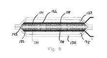
図8〜図10を参照すれば、このプラズマ蒸着方法によって製造された燃料電池の一実施例が示されている。この実施例は、基板130上に導電性層及び触媒層を形成する段階と、次いで、この触媒層上に重合体陽子交換膜を形成する段階と、次いで、この重合体陽子交換膜上に更なる触媒及び導電性層を形成する段階と、を有している。反応剤である燃料、空気、及び水を搬送するための燃料チャネル133及び空気チャネル135として機能する統合多孔性LCPチャネル131を有する液晶ポリマー(LCP)タイプのプラスチックケースを基板材料として使用している。このようなLCPケースは、型成形、熱成形、又は押出成形可能である。ポリブタジエン(PBD)やポリエチレンなどの型成形又は熱成形可能なその他の重合体材料を基板として使用することも可能である。この基板を図4に示されている装置などの蒸着装置に配置又はスプーリングする。そして、触媒の触媒反応度を向上させるべく(又は、電子伝導性陽極として)、このLCPプラスチック基板上に、グラファイト、炭素ナノチューブ、DLC(Diamond−Like Carbon)、又はこれらの組み合わせの形態の炭素層132を蒸着する。この炭素層は、真空アーク蒸着装置内に炭素材料からなる陰極を配置した後に、この炭素ターゲット材料を蒸発させ、LCPプラスチック基板上に所望の粒子サイズ及び分散によって炭素粒子を蒸着することにより、蒸着する。尚、これらの炭素粒子は、基板の一方の面又は他方の面に蒸着可能であり、或いは、同時に両面に蒸着することも可能である。
Referring to FIGS. 8 to 10, an embodiment of a fuel cell manufactured by this plasma deposition method is shown. This embodiment includes the steps of forming a conductive layer and a catalyst layer on the
その後、所望の金属からなる陰極を蒸着装置内に配置した後に、このターゲット金属を蒸発させ、所望のサイズの金属粒子を炭素層上に蒸着することにより、触媒金属層を炭素層132内に蒸着する。サイズがナノ粒子の範囲の個別中性粒子を蒸着すると、触媒の活動レベルを上げることができる。この触媒金属又は合金は、VIII族の金属又は酸化物、或いは金属の組み合わせであってよい。但し、大部分の燃料電池用途においては、触媒金属は、Pt又はこの合金、或いは、Ru−Pt又はこの合金であり、触媒効率を向上させるのに必要とされる周期表のVIII族又はその他の族の1つ又は複数のその他の金属又は酸化物を含むことも可能である。Ru−Ptタイプの触媒に加え、VIII族の酸化物層134を蒸着することにより、良好な結果を得ることができる。
Thereafter, after placing a cathode made of a desired metal in a vapor deposition apparatus, the target metal is evaporated, and metal particles of a desired size are vapor-deposited on the carbon layer, whereby a catalytic metal layer is vapor deposited in the
この触媒金属層の前、又はこれに続いて、金、炭素、又はその他の導電性材料の多孔性層138を蒸着し、燃料電池を通じた電子フローを向上させる。この層は、金、炭素、又はその他の導電性材料からなる陰極を真空アーク蒸着装置内に配置した後に、このターゲット陰極材料を蒸発させ、材料を触媒の金属層上に蒸着することにより、同様に形成される。
Prior to or following this catalytic metal layer, a
そして、反応ガスを真空チャンバの一区画内に導入し、プラズマを使用してガスを重合させて、固体重合体膜層145を形成及び蒸着することにより、1つ又は複数の固体重合体膜層140、142、及び144を多孔性導電性層上に蒸着する。使用する反応ガスは、例えば、トリフルオロメチルスルホン酸、又はクロロトリフルオロエチレン化合物である。これらのガスは、メタンなどのその他の炭化水素ガスと組み合わせて使用可能である。通常、2〜10mTのガスフロー圧力を使用する。この固体重合体膜は、陽子伝導性を有しており、燃料電池において陽子交換膜として機能する。
One or more solid polymer film layers are then formed by introducing a reaction gas into a compartment of the vacuum chamber and polymerizing the gas using plasma to form and deposit a solid
この固体重合体膜上において、触媒金属層134と導電性炭素層132、138の形成を反復し、固体重合体陽子交換膜のそれぞれの面上に触媒金属及び導電性炭素層を有する構造を形成可能である。尚、図8には、説明を目的として、層132〜150は、個別層として示されているが、それぞれの連続する層を先行する層内に分散させ、この結果、図9に示されているように、一体化した層を有する燃料電池を製造可能であることを理解されたい。別の実施例においては、この陽子交換膜上に触媒金属及び導電性炭素層を形成するプロセスを反復する代わりに、陽子交換膜を形成した後に、図9に示されているように、重合体膜層が対向し、基板の端部が密封されて燃料電池が形成されるように、基板を折り畳むことができる。重合体膜の両面に同一の一貫性を有する層を具備する必要がある場合には、この基板の折り畳みにより、完成したセルの両面がアライメントされ、有利である。
On this solid polymer membrane, formation of the
この蒸着装置は、所望のターゲット材料からなる1つの陰極によって稼働可能であるが、真空チャンバを3つ以上の区画に分割し、それぞれの区画に、炭素、触媒金属、及び導電性金属の個々の層を蒸着するターゲット陰極を供給すれば、燃料電池及びその他の用途において、本装置の効率的な稼働を実現することができる。図11には、3つ以上の別個の陰極を採用した装置の実施例が示されている(わかりやすくするべく、この図には、陽極構造が省略されている)。この実施例においては、基板101は、ロール又はスプール102から巻き出され、真空チャンバ104内に供給されるシートの形態になっている。複数のローラー106が真空チャンバの周囲に間隔をおいて配置されており、真空チャンバの周囲において3つ以上の別個の蒸着ステーション110、112、及び114をそれぞれ通じて、シート材料を搬送している。第1のステーション110は、例えば、炭素層を蒸着するべく、グラファイト材料からなる陰極116を採用している。次のステーション112は、この炭素層上に触媒層を蒸着するべく、所望の触媒金属からなる陰極118を採用している。そして、第3のステーション114は、例えば、この触媒イレヤ上に導電性層を蒸着するべく、所望の導電性材料からなる陰極120を採用している。次いで、この基板は、プラズマ重合/スルホン化領域122に進み、ここで、重合体陽子交換膜が蒸着される。次いで、この基板は、巻き上げられてロール又はスプール124となるか、或いは、そのセルの仕様に応じて、蒸着プロセスを反復することも可能である。本発明の別の実施例においては、基板の経済的なスプーリングと基板シートの他方の面への反転が可能になっており、機器及びターゲット材料の費用を削減している。又、炭素の前に、金又はその他の導電材料を低廉に蒸着し、導電性を向上させることも可能である。
The vapor deposition apparatus can be operated with a single cathode made of the desired target material, but divides the vacuum chamber into three or more compartments, each of which contains individual carbon, catalytic metal, and conductive metal. If the target cathode for depositing the layer is supplied, efficient operation of the apparatus can be realized in fuel cells and other applications. FIG. 11 shows an embodiment of an apparatus that employs three or more separate cathodes (for clarity, the anode structure is omitted in this figure). In this embodiment, the
一般的に、この蒸着プロセスは、完成した燃料電池スタックに対してどのような方向からでも遂行可能であって、いずれの端部が基板であってよい。又、本装置は、マクロ粒子のみを蒸着すると共に、プロセスパラメータによってマクロ粒子のサイズを制御可能な構成においても稼働可能である。このモードの用途の目的は、様々な粒子サイズからなる分散した触媒の高い表面領域を有するナノ構造を生成し、燃料電池における反応度効率を最適化することである。炭素のナノ構造に続いて、プラチナの個別サイズの粒子を分散させ、これに続いて、別の粒子サイズのルテニウムを分散させ、これに続いて、電子伝導用の金の非晶質連続薄膜を生成することができる。その他の実施例には、予め型成形又は押出成形されたポリエーテルスルホンイオン導電性重合体を基板陽子交換膜として使用し、この重合体基板の両面上に触媒金属及び導電性炭素層を同時に又は連続して蒸着する段階が含まれている。 In general, this deposition process can be performed from any direction with respect to the completed fuel cell stack, and either end may be a substrate. In addition, this apparatus can be operated in a configuration in which only the macro particles are deposited and the size of the macro particles can be controlled by the process parameters. The purpose of this mode of application is to produce nanostructures with a high surface area of dispersed catalyst of various particle sizes to optimize the reactivity efficiency in fuel cells. Following the carbon nanostructure, platinum individual sized particles are dispersed, followed by another particle sized ruthenium, followed by a gold continuous amorphous film for electron conduction. Can be generated. In other embodiments, a pre-molded or extruded polyethersulfone ion conductive polymer is used as a substrate proton exchange membrane, and a catalytic metal and a conductive carbon layer are formed on both sides of the polymer substrate simultaneously or simultaneously. A continuous deposition step is included.
燃料、空気、及び水チャネルを連続的に相互成層及び積層し共通マニホルドを形成可能な構成において個別の燃料電池を複数セルとして積層することができる。図10に、このような燃料電池スタックが示されている。スタックを組み立てた後に、燃料電池に空気及び燃料をそれぞれ導入するための注入口154、156、並びに燃料電池からそれぞれ燃料及び空気を排出するための排出口158、160を燃料スタック層を貫通して挿入可能である。それぞれの燃料電池又は燃料電池の組み合わせを超音波加熱又はオーバーモールドし、セルの端部を密封して、燃料スタックに構造的な完全性を付与することができる。
Individual fuel cells can be stacked as multiple cells in a configuration that allows fuel, air, and water channels to be continuously stratified and stacked to form a common manifold. FIG. 10 shows such a fuel cell stack. After the stack is assembled,
次の例は、燃料電池を製造する方法を示すものである。図7に類似した装置を使用し、LCPの基板に5〜10ナノメートルの炭素ナノ粒子を蒸着する。この蒸着プロセスにおいては、第1陽極に対して、電流を0〜50A供給し、第2陽極構造に対しては、50〜150Aの電流を供給し、第3陽極は、接地電位に設定する。そして、陰極に対する電流は、240Aとし、真空チャンバのガス圧は、7.0×10⁻⁴Tollとする。次いで、この炭素について使用したものと同様のプロセス条件下において、触媒反応度を向上させるべく、小さな粒子サイズに対して調節されたパラメータにより、Pd、Pt、Ruの分散した触媒ナノ粒子を炭素上に蒸着する。そして、2〜10mTの圧力において、パワー5〜100Wのパルス化された13.56MHzのRFプラズマ重合により、イオノマー層とスルホン化を遂行する。プラックスエア社(Praxair)から市販されているフッ化炭素ガスとVWRサイエンティフィック社(VWR Scientific)から販売されているスルホン酸溶液を30sccmに設定したマスフローコントローラを通じて導入し、パーフルオロ化された陽子交換膜を生成する。 The following example shows a method of manufacturing a fuel cell. An apparatus similar to FIG. 7 is used to deposit 5-10 nanometer carbon nanoparticles on the substrate of the LCP. In this vapor deposition process, a current of 0 to 50 A is supplied to the first anode, a current of 50 to 150 A is supplied to the second anode structure, and the third anode is set to the ground potential. The current to the cathode is 240 A, and the gas pressure in the vacuum chamber is 7.0 × 10 −4 Toll. The Pd, Pt, and Ru dispersed catalyst nanoparticles are then deposited on the carbon with parameters adjusted for small particle size to improve catalytic reactivity under the same process conditions used for this carbon. Vapor deposition. Then, the ionomer layer and sulfonation are performed by pulsed 13.56 MHz RF plasma polymerization with a power of 5 to 100 W at a pressure of 2 to 10 mT. Perfluorinated protons introduced through a mass flow controller set at 30 sccm with a fluorocarbon gas commercially available from Praxair and a sulfonic acid solution marketed by VWR Scientific (VWR Scientific) Generate an exchange membrane.
本発明を使用して一体化された燃料電池の様々な層を形成することにより、連続的なプロセスを使用して、燃料電池を非常に大規模に製造することが可能になる。又、この方法によれば、正確な量の金属触媒、導電性材料、及び陽子交換イオノマー材料によって層を正確に形成することにより、大きな接着力、良好な耐食性、容積当たりの大きな出力、少ない燃料のクロスオーバー、及び大きなイオン交換効率が提供される。 By forming the various layers of an integrated fuel cell using the present invention, it is possible to manufacture the fuel cell on a very large scale using a continuous process. Also, according to this method, by accurately forming the layer with the exact amount of metal catalyst, conductive material, and proton exchange ionomer material, great adhesion, good corrosion resistance, large output per volume, low fuel Crossover and high ion exchange efficiency.
以上、特定の実施例を参照し、本発明について説明したが、当業者であれば、本発明の真の精神及び範囲を逸脱することなく、様々な変更や変形を加えると共に、等価物による置換が可能であることを理解するであろう。従って、このようなすべての変更も添付の特許請求の範囲に含まれている。 Although the present invention has been described with reference to specific embodiments, those skilled in the art will make various changes and modifications and substitutions by equivalents without departing from the true spirit and scope of the present invention. You will understand that is possible. Accordingly, all such modifications are included within the scope of the appended claims.
本発明の固有の特徴及び利点は、以下の添付図面との関連で、本明細書の説明を参照することにより、明らかとなるであろう。
Claims (20)
(a)真空チャンバと、
(b)前記真空チャンバ内に配設され、ターゲット材料から構成された陰極であって、電力を供給されて電気アークを生成し、前記成分粒子のプラズマを生成する陰極と、
(c)前記真空チャンバ内に配設された少なくとも1つの第1陽極であって、前記陰極と前記第1陽極間に電磁場を生成し、前記帯電した成分粒子のフローをガイドする少なくとも1つの第1陽極と、
(d)前記第1陽極に隣接配置された少なくとも1つの第2陽極構造であって、電磁場を生成し、前記帯電した成分粒子を蒸着のために前記基板にガイドする少なくとも1つの第2陽極構造と、
(e)前記第2陽極に隣接して配置され、前記基板に対する中性成分粒子のフローを制御する少なくとも1つの壁及びスクリーンと、
を有するプラズマ蒸着装置。 A plasma deposition apparatus for applying one or more thin film materials in or on a substrate by selectively controlling the deposition of plasma components from the cathode to the substrate,
(A) a vacuum chamber;
(B) a cathode disposed in the vacuum chamber and made of a target material, the cathode being supplied with electric power to generate an electric arc and generating a plasma of the component particles;
(C) at least one first anode disposed in the vacuum chamber, which generates an electromagnetic field between the cathode and the first anode and guides the flow of the charged component particles. 1 anode,
(D) at least one second anode structure disposed adjacent to the first anode, wherein the at least one second anode structure generates an electromagnetic field and guides the charged component particles to the substrate for deposition. When,
(E) at least one wall and screen disposed adjacent to the second anode and controlling the flow of neutral component particles to the substrate;
A plasma deposition apparatus having:
(a)真空チャンバと、
(b)前記真空チャンバ内に配設され、ターゲット材料から構成された陰極であって、電力を供給されて電気アークを生成し、成分粒子のプラズマを生成する陰極と、
(c)前記真空チャンバ内に配設された少なくとも1つの第1陽極であって、前記陰極と前記第1陽極間に電磁場を生成し、前記帯電した成分粒子のフローをガイドする少なくとも1つの第1陽極と、
(d)前記第1陽極に隣接配置された少なくとも1つの第2陽極構造であって、電磁場を生成し、前記帯電した成分粒子を蒸着するべく前記基板にガイドする少なくとも1つの第2陽極構造と、
(e)前記第2陽極に隣接して配置され、前記基板に対する中性成分粒子のフローを制御する少なくとも1つの壁及び少なくとも1つのスクリーンと、
(f)前記第2陽極構造の一端部に隣接して配置され、電磁場を生成して電子成分粒子のフローを制御する少なくとも1つの第3陽極構造と、
を有する装置。 A plasma deposition apparatus that applies one or more materials in or on a substrate by selectively controlling the deposition of plasma particles from the cathode to the substrate,
(A) a vacuum chamber;
(B) a cathode disposed in the vacuum chamber and composed of a target material, the cathode being supplied with electric power to generate an electric arc and generating a plasma of component particles;
(C) at least one first anode disposed in the vacuum chamber, which generates an electromagnetic field between the cathode and the first anode and guides the flow of the charged component particles. 1 anode,
(D) at least one second anode structure disposed adjacent to the first anode, wherein the at least one second anode structure generates an electromagnetic field and guides the charged component particles to the substrate for vapor deposition; ,
(E) at least one wall and at least one screen disposed adjacent to the second anode and controlling the flow of neutral component particles to the substrate;
(F) at least one third anode structure disposed adjacent to one end of the second anode structure and generating an electromagnetic field to control the flow of electronic component particles;
Having a device.
(a)離隔した関係で前記陰極と前記基板とを真空チャンバ内に取り付ける段階と、
(b)前記真空チャンバ内に前記陰極を取り囲む少なくとも1つの第1陽極構造を設ける段階であって、該第1陽極構造に隣接して、少なくとも1つの第2電極構造が配置され、該第2陽極に隣接して、調節可能な開口部を具備するスクリーンを有する壁コンポーネントが配置される段階と、
(c)前記陰極に電力を供給して電気アークを生成し、荷電粒子を含む成分ターゲット粒子のプラズマを生成する段階と、
(d)前記陰極と前記第1陽極間に電磁場を生成し、前記荷電粒子のフローをガイドする段階と、
(e)前記第2陽極構造の周囲に電磁場を生成し、前記荷電粒子を前記基板にガイドする段階と、
(f)前記スクリーンの前記開口部を調節し、前記基板に対する中性粒子のフローを制御する段階と、
を有する方法。 A plasma deposition method of applying particles of the target material evaporated from a cathode of a selected target material in or on a surface of a substrate,
(A) mounting the cathode and the substrate in a vacuum chamber in a spaced relationship;
(B) providing at least one first anode structure surrounding the cathode in the vacuum chamber, wherein at least one second electrode structure is disposed adjacent to the first anode structure; A wall component having a screen with an adjustable opening is disposed adjacent to the anode;
(C) supplying electric power to the cathode to generate an electric arc and generating plasma of component target particles including charged particles;
(D) generating an electromagnetic field between the cathode and the first anode to guide the flow of the charged particles;
(E) generating an electromagnetic field around the second anode structure and guiding the charged particles to the substrate;
(F) adjusting the opening of the screen to control the flow of neutral particles to the substrate;
Having a method.
(a)グラファイト材料の陰極を蒸発させて成分粒子のプラズマを生成し、少なくとも1つの第1陽極及び1つの第2陽極によって生成された電磁場によって前記粒子を前記基板にガイドすることにより、前記基板上に炭素層を蒸着する段階と、
(b)金属材料の陰極を蒸発させて成分粒子のプラズマを生成し、前記少なくとも第1陽極及び第2陽極によって生成された前記電磁場によって前記成分粒子を前記基板にガイドすることにより、前記炭素層上にマイクロ粒子の金属触媒層を蒸着する段階と、
(c)前記真空チャンバ内に反応ガスを導入し、前記金属触媒層上に固体重合体膜層を形成する段階と、
(d)段階(a)及び段階(b)を反復して前記燃料電池を形成する段階と、
を実行する方法。 A method of manufacturing a fuel cell, for a selected substrate in a vacuum chamber,
(A) generating a plasma of component particles by evaporating a cathode of graphite material and guiding the particles to the substrate by an electromagnetic field generated by at least one first anode and one second anode; Depositing a carbon layer thereon;
(B) generating a plasma of component particles by evaporating a cathode of a metal material, and guiding the component particles to the substrate by the electromagnetic field generated by the at least first and second anodes. Depositing a microparticle metal catalyst layer thereon;
(C) introducing a reaction gas into the vacuum chamber to form a solid polymer film layer on the metal catalyst layer;
(D) repeating steps (a) and (b) to form the fuel cell;
How to run.
Applications Claiming Priority (3)
| Application Number | Priority Date | Filing Date | Title |
|---|---|---|---|
| US33568901P | 2001-11-15 | 2001-11-15 | |
| US37689302P | 2002-05-01 | 2002-05-01 | |
| PCT/US2002/036788 WO2003044240A1 (en) | 2001-11-15 | 2002-11-15 | Ionic plasma deposition apparatus |
Publications (1)
| Publication Number | Publication Date |
|---|---|
| JP2005509752A true JP2005509752A (en) | 2005-04-14 |
Family
ID=26989841
Family Applications (1)
| Application Number | Title | Priority Date | Filing Date |
|---|---|---|---|
| JP2003545857A Pending JP2005509752A (en) | 2001-11-15 | 2002-11-15 | Ion plasma deposition system |
Country Status (5)
| Country | Link |
|---|---|
| EP (1) | EP1456432A1 (en) |
| JP (1) | JP2005509752A (en) |
| KR (1) | KR20050044500A (en) |
| AU (1) | AU2002366086A1 (en) |
| WO (1) | WO2003044240A1 (en) |
Cited By (7)
| Publication number | Priority date | Publication date | Assignee | Title |
|---|---|---|---|---|
| JP2007179963A (en) * | 2005-12-28 | 2007-07-12 | Kasatani:Kk | Manufacturing method of catalyst for fuel cell and supporting method of catalyst |
| JP2009045528A (en) * | 2007-08-16 | 2009-03-05 | Ulvac Japan Ltd | Nanoparticle carrying device and coaxial carrying method with coaxial vacuum arc deposition source |
| JP2009528082A (en) * | 2006-02-25 | 2009-08-06 | カメレオン サイエンティフィック コーポレイション | UV active antibacterial surface |
| JP2009542261A (en) * | 2006-03-27 | 2009-12-03 | カメレオン サイエンティフィック コーポレイション | Improved surface for the attachment of biological materials |
| KR101362860B1 (en) | 2012-10-04 | 2014-02-21 | 주식회사 알지비하이텍 | A flatness correct equipment |
| KR101445743B1 (en) | 2008-04-04 | 2014-11-03 | 참엔지니어링(주) | Plasma processing apparatus and plasma processing method |
| JP2020066800A (en) * | 2018-10-24 | 2020-04-30 | ベイパー テクノロジーズ、インコーポレイテッド | Plasma passage for high-capacity plasma cvd processing |
Families Citing this family (34)
| Publication number | Priority date | Publication date | Assignee | Title |
|---|---|---|---|---|
| CA2635062C (en) | 2002-12-18 | 2010-10-26 | Chameleon Scientific Corporation | Antimicrobial coating methods |
| US8066854B2 (en) | 2002-12-18 | 2011-11-29 | Metascape Llc | Antimicrobial coating methods |
| FR2894076B1 (en) * | 2005-11-30 | 2014-07-11 | Centre Nat Rech Scient | PROCESS FOR PRODUCING, BY DEPOSITION ON A SUPPORT, ELECTRODE FOR A FUEL CELL |
| EP1996744B1 (en) * | 2006-01-27 | 2011-02-23 | NanoSurface Technologies, LLC | Antimicrobial coating methods |
| US20070178222A1 (en) * | 2006-01-30 | 2007-08-02 | Storey Daniel M | Radiopaque coatings for polymer substrates |
| US9422622B2 (en) | 2006-01-30 | 2016-08-23 | Surfatek Llc | Flexible conductive single wire |
| ITAT20060002A1 (en) | 2006-02-16 | 2007-08-17 | Demo Giovanni Garzino | NON-POLLUTING DEVICE FOR COATING MATERIALS. |
| US20070207310A1 (en) * | 2006-03-03 | 2007-09-06 | Storey Daniel M | Chrome coated surfaces and deposition methods therefor |
| US20080160208A1 (en) * | 2006-12-29 | 2008-07-03 | Michael Patrick Maly | System and method for restoring or regenerating an article |
| PT2251454E (en) | 2009-05-13 | 2014-10-01 | Sio2 Medical Products Inc | Vessel coating and inspection |
| US9458536B2 (en) | 2009-07-02 | 2016-10-04 | Sio2 Medical Products, Inc. | PECVD coating methods for capped syringes, cartridges and other articles |
| FR2959610B1 (en) | 2010-04-30 | 2013-01-04 | Dreux Agglomeration | METHOD FOR DEPOSITING A CATALYTIC LAYER FOR A FUEL CELL |
| US11624115B2 (en) | 2010-05-12 | 2023-04-11 | Sio2 Medical Products, Inc. | Syringe with PECVD lubrication |
| US9878101B2 (en) | 2010-11-12 | 2018-01-30 | Sio2 Medical Products, Inc. | Cyclic olefin polymer vessels and vessel coating methods |
| US20120199070A1 (en) * | 2011-02-03 | 2012-08-09 | Vapor Technologies, Inc. | Filter for arc source |
| US9272095B2 (en) | 2011-04-01 | 2016-03-01 | Sio2 Medical Products, Inc. | Vessels, contact surfaces, and coating and inspection apparatus and methods |
| WO2013071138A1 (en) | 2011-11-11 | 2013-05-16 | Sio2 Medical Products, Inc. | PASSIVATION, pH PROTECTIVE OR LUBRICITY COATING FOR PHARMACEUTICAL PACKAGE, COATING PROCESS AND APPARATUS |
| US11116695B2 (en) | 2011-11-11 | 2021-09-14 | Sio2 Medical Products, Inc. | Blood sample collection tube |
| EP2846755A1 (en) | 2012-05-09 | 2015-03-18 | SiO2 Medical Products, Inc. | Saccharide protective coating for pharmaceutical package |
| US20150297800A1 (en) | 2012-07-03 | 2015-10-22 | Sio2 Medical Products, Inc. | SiOx BARRIER FOR PHARMACEUTICAL PACKAGE AND COATING PROCESS |
| US9664626B2 (en) | 2012-11-01 | 2017-05-30 | Sio2 Medical Products, Inc. | Coating inspection method |
| EP2920567B1 (en) | 2012-11-16 | 2020-08-19 | SiO2 Medical Products, Inc. | Method and apparatus for detecting rapid barrier coating integrity characteristics |
| US9764093B2 (en) | 2012-11-30 | 2017-09-19 | Sio2 Medical Products, Inc. | Controlling the uniformity of PECVD deposition |
| CN105705676B (en) | 2012-11-30 | 2018-09-07 | Sio2医药产品公司 | Control the uniformity of the PECVD depositions on injector for medical purpose, cylindrantherae etc. |
| WO2014134577A1 (en) | 2013-03-01 | 2014-09-04 | Sio2 Medical Products, Inc. | Plasma or cvd pre-treatment for lubricated pharmaceutical package, coating process and apparatus |
| KR102167557B1 (en) | 2013-03-11 | 2020-10-20 | 에스아이오2 메디컬 프로덕츠, 인크. | Coated Packaging |
| US9937099B2 (en) | 2013-03-11 | 2018-04-10 | Sio2 Medical Products, Inc. | Trilayer coated pharmaceutical packaging with low oxygen transmission rate |
| US9863042B2 (en) | 2013-03-15 | 2018-01-09 | Sio2 Medical Products, Inc. | PECVD lubricity vessel coating, coating process and apparatus providing different power levels in two phases |
| EP3122917B1 (en) | 2014-03-28 | 2020-05-06 | SiO2 Medical Products, Inc. | Antistatic coatings for plastic vessels |
| CA2995225C (en) | 2015-08-18 | 2023-08-29 | Sio2 Medical Products, Inc. | Pharmaceutical and other packaging with low oxygen transmission rate |
| DE102017213404A1 (en) * | 2017-08-02 | 2019-02-07 | Fraunhofer-Gesellschaft zur Förderung der angewandten Forschung e.V. | Arrangement for coating substrate surfaces by means of electric arc discharge |
| CN108330464B (en) * | 2018-02-26 | 2023-10-31 | 温州职业技术学院 | Wire rod diamond-like coating processingequipment |
| KR102539000B1 (en) * | 2020-04-01 | 2023-06-05 | 국일그래핀 주식회사 | Large area graphene layer deposition apparatus |
| KR102798852B1 (en) | 2022-12-01 | 2025-04-23 | 주식회사 이온플럭스 | Centered Arc Ion Plating Evaporator |
Family Cites Families (4)
| Publication number | Priority date | Publication date | Assignee | Title |
|---|---|---|---|---|
| AT376460B (en) * | 1982-09-17 | 1984-11-26 | Kljuchko Gennady V | PLASMA ARC DEVICE FOR APPLYING COVERS |
| JPH0772338B2 (en) * | 1990-12-25 | 1995-08-02 | 株式会社神戸製鋼所 | Vacuum arc deposition equipment |
| US5269898A (en) * | 1991-03-20 | 1993-12-14 | Vapor Technologies, Inc. | Apparatus and method for coating a substrate using vacuum arc evaporation |
| DE19600933C2 (en) * | 1996-01-12 | 2002-01-10 | Wagon Automotive Gmbh | Passenger car |
-
2002
- 2002-11-15 EP EP02803641A patent/EP1456432A1/en not_active Withdrawn
- 2002-11-15 KR KR1020047007483A patent/KR20050044500A/en not_active Withdrawn
- 2002-11-15 AU AU2002366086A patent/AU2002366086A1/en not_active Abandoned
- 2002-11-15 WO PCT/US2002/036788 patent/WO2003044240A1/en not_active Ceased
- 2002-11-15 JP JP2003545857A patent/JP2005509752A/en active Pending
Cited By (8)
| Publication number | Priority date | Publication date | Assignee | Title |
|---|---|---|---|---|
| JP2007179963A (en) * | 2005-12-28 | 2007-07-12 | Kasatani:Kk | Manufacturing method of catalyst for fuel cell and supporting method of catalyst |
| JP2009528082A (en) * | 2006-02-25 | 2009-08-06 | カメレオン サイエンティフィック コーポレイション | UV active antibacterial surface |
| JP2009542261A (en) * | 2006-03-27 | 2009-12-03 | カメレオン サイエンティフィック コーポレイション | Improved surface for the attachment of biological materials |
| JP2009045528A (en) * | 2007-08-16 | 2009-03-05 | Ulvac Japan Ltd | Nanoparticle carrying device and coaxial carrying method with coaxial vacuum arc deposition source |
| KR101445743B1 (en) | 2008-04-04 | 2014-11-03 | 참엔지니어링(주) | Plasma processing apparatus and plasma processing method |
| KR101362860B1 (en) | 2012-10-04 | 2014-02-21 | 주식회사 알지비하이텍 | A flatness correct equipment |
| JP2020066800A (en) * | 2018-10-24 | 2020-04-30 | ベイパー テクノロジーズ、インコーポレイテッド | Plasma passage for high-capacity plasma cvd processing |
| JP7357474B2 (en) | 2018-10-24 | 2023-10-06 | ベイパー テクノロジーズ、インコーポレイテッド | Plasma passage for large capacity plasma CVD processing |
Also Published As
| Publication number | Publication date |
|---|---|
| EP1456432A1 (en) | 2004-09-15 |
| WO2003044240A1 (en) | 2003-05-30 |
| KR20050044500A (en) | 2005-05-12 |
| AU2002366086A1 (en) | 2003-06-10 |
Similar Documents
| Publication | Publication Date | Title |
|---|---|---|
| JP2005509752A (en) | Ion plasma deposition system | |
| US20040134770A1 (en) | Ionic plasma deposition apparatus | |
| US6351075B1 (en) | Plasma processing apparatus having rotating magnets | |
| KR101166570B1 (en) | Apparatus and method for manufacturing carbon structure | |
| CZ290081B6 (en) | Process for producing razor blade | |
| JP7520115B2 (en) | Method and apparatus for sputter depositing a target material onto a substrate - Patents.com | |
| CN1993490A (en) | Apparatus for directing plasma flow to coat internal passageways | |
| JPWO2007139086A1 (en) | Carbon nanotube growth substrate, carbon nanotube growth method, carbon nanotube growth catalyst particle size control method, and carbon nanotube diameter control method | |
| JP2001028244A (en) | Beam source | |
| US12460300B2 (en) | Method and apparatus for sputter deposition of target material to a substrate | |
| JP6625728B2 (en) | Plasma generator | |
| US20150292080A1 (en) | Apparatus for the generation of nanocluster films and methods for doing the same | |
| JP2021528815A (en) | Single beam plasma source | |
| US20030193031A1 (en) | Filtered ion source | |
| JP5420835B2 (en) | Plasma generator and film forming method using the same | |
| CN112359330A (en) | Ion coating device with scanning coil | |
| TWI254959B (en) | Film-forming apparatus and film-forming method | |
| CN100564252C (en) | Gas atom-encapsulated fullerene manufacturing device, manufacturing method, and gas atom-encapsulated fullerene | |
| US6342131B1 (en) | Method of depositing a multilayer thin film by means of magnetron sputtering which controls the magnetic field | |
| CN214142510U (en) | Ion Coating Unit with Scanning Coil | |
| CN118957507B (en) | Multipole magnetic coil charged particle beam scanning device and method | |
| JP2005068554A (en) | Thin film manufacturing method and manufacturing apparatus | |
| JP3803756B2 (en) | Soft landing method for cluster ion species | |
| CN118957508B (en) | A single-pole magnetic coil charged particle beam scanning device and method | |
| US20070110644A1 (en) | System for manufacturing a fullerene derivative and method for manufacturing |
Legal Events
| Date | Code | Title | Description |
|---|---|---|---|
| A621 | Written request for application examination |
Free format text: JAPANESE INTERMEDIATE CODE: A621 Effective date: 20051108 |
|
| A977 | Report on retrieval |
Free format text: JAPANESE INTERMEDIATE CODE: A971007 Effective date: 20080702 |
|
| A131 | Notification of reasons for refusal |
Free format text: JAPANESE INTERMEDIATE CODE: A131 Effective date: 20081209 |
|
| A02 | Decision of refusal |
Free format text: JAPANESE INTERMEDIATE CODE: A02 Effective date: 20090526 |