JP2005209729A - PCB mounting structure - Google Patents
PCB mounting structure Download PDFInfo
- Publication number
- JP2005209729A JP2005209729A JP2004012312A JP2004012312A JP2005209729A JP 2005209729 A JP2005209729 A JP 2005209729A JP 2004012312 A JP2004012312 A JP 2004012312A JP 2004012312 A JP2004012312 A JP 2004012312A JP 2005209729 A JP2005209729 A JP 2005209729A
- Authority
- JP
- Japan
- Prior art keywords
- sub
- board
- boards
- printed circuit
- circuit board
- Prior art date
- Legal status (The legal status is an assumption and is not a legal conclusion. Google has not performed a legal analysis and makes no representation as to the accuracy of the status listed.)
- Pending
Links
Images


Landscapes
- Combinations Of Printed Boards (AREA)
- Mounting Of Printed Circuit Boards And The Like (AREA)
Abstract
【課題】 複数の子基板をプリント基板に実装するにあたって、スタッドおよびネジを共有し、ユニットの重量を軽量化し、更に子基板を実装するプリント基板の部品実装面積を確保することができるプリント基板実装構造を提供する。
【解決手段】 プリント基板3上に、スペーサとしてのスタッド4を介して複数の子基板1,11,21を実装するプリント基板実装構造において、子基板1,11,21の端面に互い違いの段差を持たせ、隣り合う子基板の端を重ねて、その重ねた部分の両方の子基板を、固定部材を用いてスタッド4に固定する。
【選択図】 図2PROBLEM TO BE SOLVED: To mount a plurality of sub-boards on a printed board, share a stud and a screw, reduce the weight of the unit, and further secure a component mounting area of the printed board for mounting the sub-board. Provide structure.
SOLUTION: In a printed circuit board mounting structure in which a plurality of sub boards 1, 11, 21 are mounted on a printed board 3 via studs 4 as spacers, staggered steps are formed on the end surfaces of the sub boards 1, 11, 21. Then, the ends of the adjacent sub-boards are overlapped, and both the sub-boards of the overlapped portion are fixed to the stud 4 using a fixing member.
[Selection] Figure 2
Description
本発明は、プリント基板上に、スペーサを介して複数の子基板を実装するプリント基板実装構造に関するものである。 The present invention relates to a printed board mounting structure in which a plurality of child boards are mounted on a printed board via spacers.
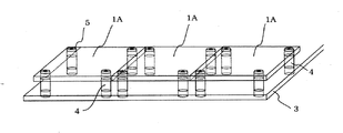
従来、プリント基板上に、スペーサとしてのスタッドを介して複数の子基板を実装する場合、それぞれの子基板の四隅をスタッドとネジで固定している(例えば、特許文献1参照)。具体的な構成を図3および図4に示す。
図3および図4において、子基板1Aは、四角形状をしており、四隅にネジ貫通穴用としてスルーホール2が形成されている。このように構成された複数の子基板1Aをプリント基板3上に実装する場合は、次のようにする。
まず、プリント基板3の、子基板1Aのスルーホール2に対応する場所に、スタッド装着用スルーホールを設け、前記スタッド装着用スルーホールに、上部にネジ穴を有するとともに外径が前記スルーホール2よりも大きいスタッド4を立てて固定する。この場合、各子基板1Aにそれぞれ4本のスタッド4が必要となる。
次に、前記スタッド4の上部先端に、子基板1Aを載置し、前記スタッド4のネジ穴の位置に前記子基板1Aのスルーホール2を合わせる。この状態で、ネジ5を子基板1のスルーホール2に通してスタッド4のネジ穴に螺合させ締め付けて、子基板1Aをプリント基板3に実装する。
3 and 4, the
First, a stud mounting through hole is provided in a place corresponding to the through
Next, the
しかしながら、このような従来技術においては、次のような問題があった。
(1)子基板は、プリント基板に対して、実装する複数の子基板それぞれの四隅で固定す る構造となっており、子基板実装枚数の4倍のスタッドを必要とするため、ユニッ トの重量が大きくなる。
(2)プリント基板に設けるスタッド装着用スルーホールも子基板実装枚数の4倍必要と なるので、プリント基板上での部品実装面積が十分に確保出来ない。
本発明は、このような問題点に鑑みてなされたもので、複数の子基板をプリント基板に実装するにあたって、スタッドおよびネジを共有し、ユニットの重量を軽量化し、更に子基板を実装するプリント基板の部品実装面積を確保することができるプリント基板実装構造を提供することを目的とするものである。
However, such conventional techniques have the following problems.
(1) The sub-board is fixed to the printed circuit board at the four corners of each of the sub-boards to be mounted, and requires four times as many studs as the number of sub-boards mounted. Increases weight.
(2) The stud mounting through-holes provided on the printed circuit board are required to be four times as many as the number of sub-boards mounted, so a sufficient component mounting area cannot be secured on the printed circuit board.
The present invention has been made in view of such problems, and in mounting a plurality of sub boards on a printed board, a stud and a screw are shared, the weight of the unit is reduced, and the sub board is mounted. It is an object of the present invention to provide a printed circuit board mounting structure capable of securing a component mounting area of a board.
上記問題を解決するため、本発明は、プリント基板上に、スペーサを介して複数の子基板を並べて実装するプリント基板実装構造において、前記子基板の並列方向の端面に互い違いの段差を持たせ、隣り合う子基板の端を重ねて、その重ねた部分の両方の子基板を、固定部材を用いて前記スペーサに固定するようにしたものである。 In order to solve the above problems, the present invention provides a printed circuit board mounting structure in which a plurality of child boards are mounted side by side via spacers on a printed circuit board, and the end faces in the parallel direction of the child boards have staggered steps. The ends of the adjacent sub-boards are overlapped, and both the sub-boards of the overlapped portion are fixed to the spacer using a fixing member.
本発明によれば、子基板固定用のスタッドおよびネジを削減することができ、ユニットの軽量化および子基板を実装するプリント基板の部品実装面積を確保することができるという効果がある。 According to the present invention, it is possible to reduce the studs and screws for fixing the sub board, and it is possible to reduce the weight of the unit and secure the component mounting area of the printed board on which the sub board is mounted.
以下、本発明の実施例を図に基づいて説明する。 Embodiments of the present invention will be described below with reference to the drawings.
図1は、本発明の実施例における子基板の構造を示す斜視図である。図2は、本発明の実施例におけるプリント基板実装構造を示す斜視図である。
本発明においては、プリント基板上に、スペーサを介して複数の子基板を並べて実装する場合、前記子基板の並列方向の端面に互い違いの段差を持たせ、隣り合う子基板の端を重ねて、その重ねた部分の両方の子基板を、固定部材を用いて前記スペーサに固定するようにしている。具体的な構成を図1および図2に示す。
図1および図2において、四角形状をした子基板1は並列方向の端面の厚みを薄くして段差を形成している。図1に示す子基板1の右側の端面には、子基板1の上面を削り基板厚さを中央部の半分の厚さとした上側段差7を形成し、反対側の左側端面には、子基板1の下面を削り、こちらも基板厚さを中央部の半分の厚さとした下側段差7を形成している。また、前記下側段差6と上側段差7には、それぞれ幅方向の両端部にネジ貫通穴用のスルーホール2が形成されている。
従来の子基板1Aは全面同じ厚さであり、断面形状は長方形であるのに対し、本発明における子基板1は並列方向の端面の厚さを中央部分の厚さの半分とした互い違いの段差を持たせるように加工している。
前記下側段差6および上側段差7を形成することにより、同一の複数の子基板をプリント基板に実装するにあたって、スタッドおよびネジを共有することができる。
すなわち、図2に示すように、子基板1と同一で、前記子基板1に隣接する子基板を11、更に子基板11と同一で、前記子基板11に隣接する子基板を21とすると、子基板1の上側段差7と、隣接する子基板21の下側段差16とを重ね合わせることができ、子基板1の上側段差7に設けられたスルーホール2と、隣接する子基板11の下側段差16に設けられたスルーホール12とが一致する。これにより隣接する子基板1および子基板11がそれぞれに有する4つのスルーホール2、12のうち2つが一致することとなり、このスルーホール12の上面からネジ5でスタッド4に共締めできる構造となり、プリント基板3に装着されたスタッド4およびネジ5を共有化することができる。
同様に、子基板11に隣接する子基板21についても、子基板11の上側段差17と子基板21の下側段差26とが重ね合わさり、両子基板11,21間でスタッド4およびネジ5を共有化することができる。
これによりスタッド4及びネジ5の数を削減することができる。
なお、本実施例では、複数の子基板は同一のものを用いているが、当然ながら、同一でない複数の子基板であってもよい。
また、子基板の形状は四角に限らず、並列方向の端面を重ね合わせられる形状であればどのような形状でも構わない。
FIG. 1 is a perspective view showing the structure of a daughter board in an embodiment of the present invention. FIG. 2 is a perspective view showing a printed circuit board mounting structure in an embodiment of the present invention.
In the present invention, when mounting a plurality of sub-boards side by side through a spacer on a printed board, the staggered steps are provided on the end faces in the parallel direction of the sub-boards, and the ends of the adjacent sub-boards are overlapped, Both the child substrates in the overlapped portion are fixed to the spacer using a fixing member. A specific configuration is shown in FIGS.
In FIG. 1 and FIG. 2, the quadrilateral child substrate 1 has a step formed by reducing the thickness of the end face in the parallel direction. On the right end face of the sub-board 1 shown in FIG. 1, an upper step 7 is formed by cutting the top surface of the sub-board 1 so that the thickness of the board is half the central portion, and on the left end face on the opposite side, A lower step 7 is formed by cutting the lower surface of 1 and also having a substrate thickness half the thickness of the central portion. The
Whereas the
By forming the
That is, as shown in FIG. 2, when the sub-board 1 is the same as the sub-board 1 and is adjacent to the sub-board 1, and the sub-board 11 is the same as the sub-board 11 and is adjacent to the sub-board 11, The upper step 7 of the child substrate 1 and the lower step 16 of the adjacent child substrate 21 can be overlapped, and the through-
Similarly, for the child substrate 21 adjacent to the child substrate 11, the upper step 17 of the child substrate 11 and the
Thereby, the number of
In the present embodiment, the same plurality of sub-boards are used, but it is needless to say that a plurality of sub-boards may not be the same.
Further, the shape of the sub-board is not limited to a square, and any shape may be used as long as the end faces in the parallel direction can be superimposed.
1,1A 子基板
2 スルーホール
3 プリント基板
4 スタッド
5 ねじ
6 下側段差
7 上側段差
11 子基板
12 スルーホール
16 下側段差
17 上側段差
21 子基板
22 スルーホール
26 下側段差
27 上側段差
1, 1A
Claims (2)
前記子基板の並列方向の端面に互い違いの段差を持たせ、隣り合う子基板の端を重ねて、その重ねた部分の両方の子基板を、固定部材を用いて前記スペーサに固定したことを特徴とするプリント基板実装構造。 In a printed circuit board mounting structure in which a plurality of child boards are mounted side by side via a spacer on a printed circuit board,
It is characterized by having staggered steps on the end faces in the parallel direction of the sub-boards, overlapping the ends of the adjacent sub-boards, and fixing both the sub-boards of the overlapped parts to the spacer using a fixing member. Printed circuit board mounting structure.
Priority Applications (1)
| Application Number | Priority Date | Filing Date | Title |
|---|---|---|---|
| JP2004012312A JP2005209729A (en) | 2004-01-20 | 2004-01-20 | PCB mounting structure |
Applications Claiming Priority (1)
| Application Number | Priority Date | Filing Date | Title |
|---|---|---|---|
| JP2004012312A JP2005209729A (en) | 2004-01-20 | 2004-01-20 | PCB mounting structure |
Publications (1)
| Publication Number | Publication Date |
|---|---|
| JP2005209729A true JP2005209729A (en) | 2005-08-04 |
Family
ID=34898725
Family Applications (1)
| Application Number | Title | Priority Date | Filing Date |
|---|---|---|---|
| JP2004012312A Pending JP2005209729A (en) | 2004-01-20 | 2004-01-20 | PCB mounting structure |
Country Status (1)
| Country | Link |
|---|---|
| JP (1) | JP2005209729A (en) |
Cited By (4)
| Publication number | Priority date | Publication date | Assignee | Title |
|---|---|---|---|---|
| KR100988517B1 (en) * | 2005-10-07 | 2010-10-20 | 도요타 지도샤(주) | Fixing member for fixing a plurality of circuit boards and the module using the fixing member |
| JP2017513237A (en) * | 2014-03-21 | 2017-05-25 | ノキア テクノロジーズ オサケユイチア | Flexible electronic device and associated method |
| US10435289B2 (en) | 2014-10-16 | 2019-10-08 | Nokia Technoloiges Oy | Deformable apparatus and method |
| US12069804B2 (en) | 2019-07-22 | 2024-08-20 | Samsung Electronics Co., Ltd. | Electronic device comprising printed circuit board assembly |
-
2004
- 2004-01-20 JP JP2004012312A patent/JP2005209729A/en active Pending
Cited By (5)
| Publication number | Priority date | Publication date | Assignee | Title |
|---|---|---|---|---|
| KR100988517B1 (en) * | 2005-10-07 | 2010-10-20 | 도요타 지도샤(주) | Fixing member for fixing a plurality of circuit boards and the module using the fixing member |
| JP2017513237A (en) * | 2014-03-21 | 2017-05-25 | ノキア テクノロジーズ オサケユイチア | Flexible electronic device and associated method |
| US10470304B2 (en) | 2014-03-21 | 2019-11-05 | Nokia Technologies Oy | Flexible electronics apparatus and associated methods |
| US10435289B2 (en) | 2014-10-16 | 2019-10-08 | Nokia Technoloiges Oy | Deformable apparatus and method |
| US12069804B2 (en) | 2019-07-22 | 2024-08-20 | Samsung Electronics Co., Ltd. | Electronic device comprising printed circuit board assembly |
Similar Documents
| Publication | Publication Date | Title |
|---|---|---|
| JP4678554B2 (en) | Control device | |
| JP2006013410A (en) | Slide rail fixing arrangement of server chassis | |
| IL151278A (en) | Printed circuit board assembly | |
| JP2016162944A (en) | Printed circuit board and printed circuit board connection structure using the circuit board | |
| JP2005209729A (en) | PCB mounting structure | |
| JP2004103907A (en) | Circuit board positioning structure | |
| US20150163912A1 (en) | Mounting in circuit board | |
| KR200450073Y1 (en) | Multi assembly jig | |
| JP2007287826A (en) | Circuit board fixing structure | |
| TWI722829B (en) | Circuit board fixing structure | |
| JP2008078438A (en) | Structure for mounting printed board | |
| JP2005011158A (en) | Riser card device with expansion slots on two sides | |
| JPH04101491A (en) | Mounting method for chip component | |
| JP2001177209A (en) | Fixing structure of circuit board for stack structure | |
| JP2002134916A (en) | Laminated wiring board | |
| JPH02219299A (en) | Printed board mounting structure | |
| JP2010287821A (en) | Heat sink fitting structure | |
| JPS5832293Y2 (en) | Printed circuit board holding device | |
| KR20250027965A (en) | Pcb assembly | |
| JPH11346041A (en) | PCB and electronic equipment | |
| JPH1197808A (en) | Circuit board | |
| JPH0818292A (en) | Printed circuit board support method | |
| JP2004327494A (en) | Structure for attaching component onto printed circuit board mounted on device enclosure | |
| JP2009206263A (en) | Electronic equipment | |
| US20210064101A1 (en) | Fixing structure |