JP2005183660A - Solar cell module - Google Patents
Solar cell module Download PDFInfo
- Publication number
- JP2005183660A JP2005183660A JP2003422103A JP2003422103A JP2005183660A JP 2005183660 A JP2005183660 A JP 2005183660A JP 2003422103 A JP2003422103 A JP 2003422103A JP 2003422103 A JP2003422103 A JP 2003422103A JP 2005183660 A JP2005183660 A JP 2005183660A
- Authority
- JP
- Japan
- Prior art keywords
- photovoltaic element
- bypass diode
- photovoltaic
- conductive member
- solar cell
- Prior art date
- Legal status (The legal status is an assumption and is not a legal conclusion. Google has not performed a legal analysis and makes no representation as to the accuracy of the status listed.)
- Withdrawn
Links
- 230000007774 longterm Effects 0.000 abstract description 5
- 239000000463 material Substances 0.000 description 46
- 239000003566 sealing material Substances 0.000 description 21
- 238000010586 diagram Methods 0.000 description 20
- 239000007774 positive electrode material Substances 0.000 description 15
- 239000000758 substrate Substances 0.000 description 11
- 239000011248 coating agent Substances 0.000 description 10
- 238000000576 coating method Methods 0.000 description 10
- 238000007789 sealing Methods 0.000 description 10
- 239000010408 film Substances 0.000 description 7
- 239000004065 semiconductor Substances 0.000 description 7
- 238000000034 method Methods 0.000 description 5
- 229910021417 amorphous silicon Inorganic materials 0.000 description 4
- 238000004519 manufacturing process Methods 0.000 description 4
- RYGMFSIKBFXOCR-UHFFFAOYSA-N Copper Chemical compound [Cu] RYGMFSIKBFXOCR-UHFFFAOYSA-N 0.000 description 3
- 239000011889 copper foil Substances 0.000 description 3
- 239000007772 electrode material Substances 0.000 description 3
- 239000002184 metal Substances 0.000 description 3
- 229910052751 metal Inorganic materials 0.000 description 3
- XUIMIQQOPSSXEZ-UHFFFAOYSA-N Silicon Chemical compound [Si] XUIMIQQOPSSXEZ-UHFFFAOYSA-N 0.000 description 2
- 238000006243 chemical reaction Methods 0.000 description 2
- 239000011521 glass Substances 0.000 description 2
- 238000010438 heat treatment Methods 0.000 description 2
- 229910021424 microcrystalline silicon Inorganic materials 0.000 description 2
- 238000000465 moulding Methods 0.000 description 2
- 229910052710 silicon Inorganic materials 0.000 description 2
- 239000010703 silicon Substances 0.000 description 2
- 238000005476 soldering Methods 0.000 description 2
- 239000010409 thin film Substances 0.000 description 2
- 230000037303 wrinkles Effects 0.000 description 2
- BQCADISMDOOEFD-UHFFFAOYSA-N Silver Chemical compound [Ag] BQCADISMDOOEFD-UHFFFAOYSA-N 0.000 description 1
- KTSFMFGEAAANTF-UHFFFAOYSA-N [Cu].[Se].[Se].[In] Chemical compound [Cu].[Se].[Se].[In] KTSFMFGEAAANTF-UHFFFAOYSA-N 0.000 description 1
- 230000004888 barrier function Effects 0.000 description 1
- 238000005452 bending Methods 0.000 description 1
- 239000004566 building material Substances 0.000 description 1
- 150000001875 compounds Chemical class 0.000 description 1
- 230000007797 corrosion Effects 0.000 description 1
- 238000005260 corrosion Methods 0.000 description 1
- 229910021419 crystalline silicon Inorganic materials 0.000 description 1
- 230000007547 defect Effects 0.000 description 1
- 238000007872 degassing Methods 0.000 description 1
- 230000000694 effects Effects 0.000 description 1
- 230000005611 electricity Effects 0.000 description 1
- 230000007613 environmental effect Effects 0.000 description 1
- 239000013081 microcrystal Substances 0.000 description 1
- 229910021420 polycrystalline silicon Inorganic materials 0.000 description 1
- 229920006267 polyester film Polymers 0.000 description 1
- 238000007650 screen-printing Methods 0.000 description 1
- 229910052709 silver Inorganic materials 0.000 description 1
- 239000004332 silver Substances 0.000 description 1
- 229910000679 solder Inorganic materials 0.000 description 1
- 229910001220 stainless steel Inorganic materials 0.000 description 1
- 239000010935 stainless steel Substances 0.000 description 1
- 238000010792 warming Methods 0.000 description 1
Images


Classifications
-
- H—ELECTRICITY
- H10—SEMICONDUCTOR DEVICES; ELECTRIC SOLID-STATE DEVICES NOT OTHERWISE PROVIDED FOR
- H10F—INORGANIC SEMICONDUCTOR DEVICES SENSITIVE TO INFRARED RADIATION, LIGHT, ELECTROMAGNETIC RADIATION OF SHORTER WAVELENGTH OR CORPUSCULAR RADIATION
- H10F77/00—Constructional details of devices covered by this subclass
- H10F77/93—Interconnections
- H10F77/933—Interconnections for devices having potential barriers
- H10F77/935—Interconnections for devices having potential barriers for photovoltaic devices or modules
-
- H—ELECTRICITY
- H02—GENERATION; CONVERSION OR DISTRIBUTION OF ELECTRIC POWER
- H02S—GENERATION OF ELECTRIC POWER BY CONVERSION OF INFRARED RADIATION, VISIBLE LIGHT OR ULTRAVIOLET LIGHT, e.g. USING PHOTOVOLTAIC [PV] MODULES
- H02S40/00—Components or accessories in combination with PV modules, not provided for in groups H02S10/00 - H02S30/00
- H02S40/30—Electrical components
- H02S40/36—Electrical components characterised by special electrical interconnection means between two or more PV modules, e.g. electrical module-to-module connection
-
- H—ELECTRICITY
- H10—SEMICONDUCTOR DEVICES; ELECTRIC SOLID-STATE DEVICES NOT OTHERWISE PROVIDED FOR
- H10F—INORGANIC SEMICONDUCTOR DEVICES SENSITIVE TO INFRARED RADIATION, LIGHT, ELECTROMAGNETIC RADIATION OF SHORTER WAVELENGTH OR CORPUSCULAR RADIATION
- H10F19/00—Integrated devices, or assemblies of multiple devices, comprising at least one photovoltaic cell covered by group H10F10/00, e.g. photovoltaic modules
- H10F19/30—Integrated devices, or assemblies of multiple devices, comprising at least one photovoltaic cell covered by group H10F10/00, e.g. photovoltaic modules comprising thin-film photovoltaic cells
- H10F19/31—Integrated devices, or assemblies of multiple devices, comprising at least one photovoltaic cell covered by group H10F10/00, e.g. photovoltaic modules comprising thin-film photovoltaic cells having multiple laterally adjacent thin-film photovoltaic cells deposited on the same substrate
-
- H—ELECTRICITY
- H10—SEMICONDUCTOR DEVICES; ELECTRIC SOLID-STATE DEVICES NOT OTHERWISE PROVIDED FOR
- H10F—INORGANIC SEMICONDUCTOR DEVICES SENSITIVE TO INFRARED RADIATION, LIGHT, ELECTROMAGNETIC RADIATION OF SHORTER WAVELENGTH OR CORPUSCULAR RADIATION
- H10F19/00—Integrated devices, or assemblies of multiple devices, comprising at least one photovoltaic cell covered by group H10F10/00, e.g. photovoltaic modules
- H10F19/90—Structures for connecting between photovoltaic cells, e.g. interconnections or insulating spacers
- H10F19/902—Structures for connecting between photovoltaic cells, e.g. interconnections or insulating spacers for series or parallel connection of photovoltaic cells
- H10F19/904—Structures for connecting between photovoltaic cells, e.g. interconnections or insulating spacers for series or parallel connection of photovoltaic cells characterised by the shapes of the structures
-
- Y—GENERAL TAGGING OF NEW TECHNOLOGICAL DEVELOPMENTS; GENERAL TAGGING OF CROSS-SECTIONAL TECHNOLOGIES SPANNING OVER SEVERAL SECTIONS OF THE IPC; TECHNICAL SUBJECTS COVERED BY FORMER USPC CROSS-REFERENCE ART COLLECTIONS [XRACs] AND DIGESTS
- Y02—TECHNOLOGIES OR APPLICATIONS FOR MITIGATION OR ADAPTATION AGAINST CLIMATE CHANGE
- Y02E—REDUCTION OF GREENHOUSE GAS [GHG] EMISSIONS, RELATED TO ENERGY GENERATION, TRANSMISSION OR DISTRIBUTION
- Y02E10/00—Energy generation through renewable energy sources
- Y02E10/50—Photovoltaic [PV] energy
Landscapes
- Photovoltaic Devices (AREA)
Abstract
【課題】
光起電力素子に複数の逆方向電圧印加防止用のバイパスダイオードを接続する場合に、気泡残りなく封止することができ、外観が良好なだけでなく、屋外長期使用における信頼性を向上させることができる太陽電池モジュールを提供する。
【解決手段】
少なくとも一つの光起電力素子1と、光起電力素子1の逆方向電圧印加防止用のバイパスダイオード5と、バイパスダイオード5を配置するための導電部材2とを有する太陽電池モジュールであって、導電部材2は、対の光起電力素子側接続部10と複数系統のバイパスダイオード側接続部11とから構成され、これらバイパスダイオード側接続部11は光起電力素子接続部10、10間に並列に配されており、隣接する系統のバイパスダイオード側接続部11上に各バイパスダイオード5が互い違いに位置をずらして配置されている。
【選択図】 図1
【Task】
When connecting multiple bypass diodes to prevent reverse voltage application to the photovoltaic device, it can be sealed without bubbles remaining, and it not only has a good appearance, but also improves reliability in outdoor long-term use Provided is a solar cell module.
[Solution]
A solar cell module comprising at least one photovoltaic element 1, a bypass diode 5 for preventing reverse voltage application of the photovoltaic element 1, and a conductive member 2 for disposing the bypass diode 5. The member 2 includes a pair of photovoltaic element side connection portions 10 and a plurality of bypass diode side connection portions 11, and these bypass diode side connection portions 11 are arranged in parallel between the photovoltaic element connection portions 10 and 10. The bypass diodes 5 are alternately arranged on the bypass diode side connection portions 11 of adjacent systems.
[Selection] Figure 1
Description
本発明は、少なくとも一つの光起電力素子を備え、該光起電力素子の逆方向電圧印加防止用のバイパスダイオードを有する太陽電池モジュールに関する。 The present invention relates to a solar cell module including at least one photovoltaic element and having a bypass diode for preventing reverse voltage application of the photovoltaic element.
従来から、環境問題に対する意識の高まりが、世界的において広がりを見せている。中でも、CO2排出に伴う地球の温暖化現象に対する危惧感は深刻であり、クリーンなエネルギーへの希求はますます強まってきている。太陽電池は現在のところ、その安全性と扱い易さから、クリーンなエネルギー源として期待のもてるものであるということができる。 Traditionally, the growing awareness of environmental issues has spread worldwide. Above all, the fear of global warming due to CO 2 emissions is serious, and the demand for clean energy is increasing. At present, solar cells can be expected as a clean energy source because of their safety and ease of handling.
近年では、太陽電池装置の形態として様々な方式のものが提案されてきている。従来からの地上設置型の架台設置方式以外に、屋根上に架台を組んで太陽電池パネルを固定する方式や、また建材そのものに太陽電池を組み入れた建材一体型太陽電池に関する技術開発も行われている。 In recent years, various types of solar cell devices have been proposed. In addition to the conventional ground-mounted mounting system, technical development has also been carried out on a system that builds a mounting on the roof and fixes the solar panel, and on a building-integrated solar cell that incorporates solar cells into the building material itself. Yes.
一般的に太陽電池モジュールは、単一または複数枚の光起電力素子が被覆材により封止されており、受光面、非受光面が耐候性材料で覆われている構造を有する。電気的には光起電力素子は直並列接続されており、一般的には出力電力は交流電力へ変換後に系統電力に接続される。 Generally, a solar cell module has a structure in which a single or a plurality of photovoltaic elements are sealed with a covering material, and a light receiving surface and a non-light receiving surface are covered with a weather-resistant material. Electrically, the photovoltaic elements are connected in series and parallel, and generally the output power is connected to the system power after being converted into AC power.
このように使用されている太陽電池モジュールにおいて、一部の光起電力素子が影になった場合、影になった光起電力素子の両端には逆方向の電圧がかかる場合がある。 In the solar cell module used in this way, when some of the photovoltaic elements are shaded, a reverse voltage may be applied to both ends of the shaded photovoltaic elements.
図12は、従来の影になった光起電力素子を説明するための概略図である。図12において、31は光起電力素子、32は影になった光起電力素子、33は太陽電池モジュール、34は配線である。 FIG. 12 is a schematic diagram for explaining a conventional photovoltaic element in the shadow. In FIG. 12, 31 is a photovoltaic element, 32 is a shaded photovoltaic element, 33 is a solar cell module, and 34 is a wiring.
図示するように、一枚の光起電力素子32が影になった場合、影となった光起電力素子32には電流が流れない。その一方で、残りの光起電力素子31は光照射されているので、電気を流そうとする。そのため、影になった光起電力素子32には負荷を介して逆方向の電圧がかかることになり、場合によっては影になった光起電力素子32は損傷することになる。これを防ぐために光起電力素子31にはバイパスダイオードが接続されている。
As shown in the drawing, when one
図13は、従来のバイパスダイオードが接続された光起電力素子の断面構造を示す概略図、図14は図13の光起電力素子の概略図である。これらの図において、31は光起電力素子、41はバイパスダイオード、42は導電部材、43は正極電極材、44は半導体光起電力素子活性層、45は導電性基体、46は集電電極、47は半田である。 FIG. 13 is a schematic diagram showing a cross-sectional structure of a photovoltaic element to which a conventional bypass diode is connected, and FIG. 14 is a schematic diagram of the photovoltaic element in FIG. In these drawings, 31 is a photovoltaic element, 41 is a bypass diode, 42 is a conductive member, 43 is a positive electrode material, 44 is a semiconductor photovoltaic element active layer, 45 is a conductive substrate, 46 is a collecting electrode, 47 is solder.
図示するように、光起電力素子の導電性基体45が裏面電極材を兼ねている場合、パスダイオード41は、光起電力素子31の正極電極材43と導電性基体45との間に電気的に接続されている。また、パスダイオード41は、導電部材42により光起電力素子31と並列接続されており、光起電力素子31の逆方向に整流できる方向、すなわち、カソード電極側が正極電極材43に電気的に接続されている。
As shown in the figure, when the
以上のようにしてバイパスダイオードを形成した後に、必要に応じて光起電力素子31を直列接続あるいは並列接続してから封止する。
After forming the bypass diode as described above, the
図15は従来の光起電力素子を封止するために材料を積層している状態を示す模式図、図16は従来の一体成型封止後の太陽電池モジュールの断面構造を示す概略図である。これら図において、31は光起電力素子、41はバイパスダイオード、51は封止材、52は表面被覆材、53は裏面被覆材である。 FIG. 15 is a schematic view showing a state in which materials are laminated to seal a conventional photovoltaic element, and FIG. 16 is a schematic view showing a cross-sectional structure of a conventional solar cell module after integral molding sealing. . In these figures, 31 is a photovoltaic element, 41 is a bypass diode, 51 is a sealing material, 52 is a surface covering material, and 53 is a back surface covering material.
図15に示すように、表面被覆材52/封止材51/光起電力素子31/封止材51/裏面被覆材53を順に配し、これらを真空引きすると共に加熱することで、図16に示すように、光起電力素子31を一体成形封止することができる。
As shown in FIG. 15, the
以上のように、光起電力素子31を封止して太陽電池モジュールを作製し、光起電力素子31が屋外環境で長期間使用できるようになっている。
As described above, the
一方、光起電力素子31の変換効率が上がり電流が増えてくると、それまで使用していたバイパスダイオード41では容量不足になる場合がある。このときに、単に容量の大きなダイオード41を選択すると、ダイオード41の体積が大きくなってしまうため、太陽電池モジュールの一体成形封止後にダイオード周りに気泡残りが発生したり、あるいは、表面被覆材52にフィルムを使用した場合にはフィルムしわが発生することがある。特に、気泡残りがあると、屋外暴露環境では水分がこの気泡内に溜まって電気回路のショートや電極材の腐食に至る虞れがある。
On the other hand, when the conversion efficiency of the
以上の問題に対しては、体積が小さくて済む容量の小さなダイオード複数個を並列に接続して配置することで対処することができる。例えば、特開2000−243995号公報(特許文献1)には、光起電力素子の電流が増えた場合に、複数個のバイパスダイオードを並列に電気接続する技術が開示されている。 The above problems can be dealt with by connecting a plurality of small-capacitance diodes having a small volume in parallel. For example, Japanese Patent Application Laid-Open No. 2000-243959 (Patent Document 1) discloses a technique of electrically connecting a plurality of bypass diodes in parallel when the current of a photovoltaic element increases.
光起電力素子に対して複数個のバイパスダイオードを並列接続する方式としては、一つのバイパスダイオードに一対の導電部材を用意して、これを光起電力素子に複数個取り付ける方式と、複数個のバイパスダイオードに一対の導電部材を用意して、導電部材にバイパスダイオードを並列接続して、これを光起電力素子と並列接続する方式とが考えられる。 As a method of connecting a plurality of bypass diodes in parallel to the photovoltaic element, a pair of conductive members are prepared for one bypass diode, and a plurality of these are attached to the photovoltaic element. A method of preparing a pair of conductive members for the bypass diode, connecting the bypass diode in parallel to the conductive member, and connecting the bypass diode in parallel with the photovoltaic element is conceivable.
図17は、従来の容量の小さな複数個のダイオードを並列接続できる導電部材を用意し、これを光起電力素子に並列接続した状態を示す概略図、図18は従来の容量の小さな複数個のダイオードを並列接続して配置した光起電力素子を一体成形封止した状態の断面構造を示す概略図である。これらの図において、31は光起電力素子、41はバイパスダイオード、42は導電部材、dは光起電力素子の端部からバイパスダイオードの外側端部までの距離である。 FIG. 17 is a schematic diagram showing a state in which a conventional conductive member capable of connecting a plurality of diodes with small capacities is connected in parallel to a photovoltaic element, and FIG. It is the schematic which shows the cross-section of the state which integrally molded and sealed the photovoltaic element arrange | positioned by connecting the diode in parallel. In these drawings, 31 is a photovoltaic element, 41 is a bypass diode, 42 is a conductive member, and d is the distance from the end of the photovoltaic element to the outer end of the bypass diode.
このように構成することで、従来からの製造コストを増大させることなく、脱気不良が発生し難くなり、表面被覆材52にフィルムを使用した場合は、フィルムしわが発生し難くなる。
By comprising in this way, it becomes difficult to generate | occur | produce deaeration without increasing the manufacturing cost from the former, and when a film is used for the
しかしながら、太陽電池モジュールを製造するにあたって、コストの低減化が重要な課題となっており、太陽電池モジュールの封止材料の使用量を削減することは重要である。図17に示したように、複数個のバイパスダイオード41を並列接続しようとすると、実装工程における製造コストは変わらないが、今度はバイパスダイオード41の占める面積が増大してしまうため、その分、封止材の使用量を増加させる必要性が生じてくる。
However, in manufacturing the solar cell module, cost reduction is an important issue, and it is important to reduce the amount of the sealing material used for the solar cell module. As shown in FIG. 17, when a plurality of
そこで、封止材料の使用量をできる限り少なくするために、光起電力素子31の端部から最も離れたバイパスダイオード41の外側端部までの距離dを小さくすると共に、隣接するバイパスダイオード同士の間隔もできるだけ狭くすることが求められる。
Therefore, in order to reduce the amount of the sealing material used as much as possible, the distance d from the end of the
しかし、複数個のダイオード41を接近して配置すると、ダイオード近傍に充填不良、すなわち、気泡残りが発生するということが判明した。
However, it has been found that when a plurality of
本発明は、上記の課題に鑑みて創案されたものであり、その目的は、光起電力素子に複数の逆方向電圧印加防止用のバイパスダイオードを接続する場合に、気泡残りなく封止することができ、外観が良好なだけでなく、屋外長期使用における信頼性を向上させることができる太陽電池モジュールを提供することにある。 The present invention has been made in view of the above problems, and its purpose is to seal without any remaining bubbles when a plurality of bypass diodes for preventing reverse voltage application are connected to a photovoltaic element. It is possible to provide a solar cell module that not only has a good appearance but also can improve reliability in outdoor long-term use.
上記の目的を達成すべく、本発明に係る太陽電池モジュールは、少なくとも一つの光起電力素子と、該光起電力素子の逆方向電圧印加防止用のバイパスダイオードと、該バイパスダイオードを配置するための導電部材とを有する太陽電池モジュールにおいて、上記導電部材は、対の光起電力素子側接続部と複数系統のバイパスダイオード側接続部とから構成され、これらバイパスダイオード側接続部は上記光起電力素子接続部間に並列に配されており、隣接する系統のバイパスダイオード側接続部上に各バイパスダイオードが互い違いに位置をずらして配置されていることを特徴とする。 In order to achieve the above object, a solar cell module according to the present invention includes at least one photovoltaic element, a bypass diode for preventing reverse voltage application of the photovoltaic element, and the bypass diode. The conductive member is composed of a pair of photovoltaic element side connection parts and a plurality of bypass diode side connection parts, and these bypass diode side connection parts are formed of the photovoltaic power module. The bypass diodes are arranged in parallel between the element connection portions, and the bypass diodes are alternately arranged on the bypass diode side connection portions of adjacent systems.
また、複数の光起電力素子を直列または並列に電気的に接続して光起電力素子群が構成され、隣接する光起電力素子同士を前記導電部材が跨ぐように形成されていることが好ましい。 Moreover, it is preferable that a plurality of photovoltaic elements are electrically connected in series or in parallel to form a photovoltaic element group, and that the conductive member straddles the adjacent photovoltaic elements. .
さらに、前記光起電力素子間には間隔が設けられており、該間隔及びその延長線上の領域には前記バイパスダイオードが存在しないことが好ましい。 Furthermore, it is preferable that a space is provided between the photovoltaic elements, and the bypass diode does not exist in the space and a region on an extension line thereof.
本発明に係る太陽電池モジュールによれば、次のような優れた効果を奏する。 The solar cell module according to the present invention has the following excellent effects.
すなわち、バイパスダイオードを配置するための導電部材は、対の光起電力素子側接続部と複数系統のバイパスダイオード側接続部とから成り、これらバイパスダイオード側接続部は上記光起電力素子接続部間に並列に配され、隣接する系統のバイパスダイオード側接続部上に各バイパスダイオードが互い違いに位置をずらして配置されているので、封止時に脱気が促されて封止材の流れ込みがスムーズになり、封止する部材間に気泡が残らないように封止でき、太陽電池モジュールの外観が良好なだけでなく、屋外長期使用における太陽電池モジュールの信頼性を向上させることができる。 That is, the conductive member for disposing the bypass diode is composed of a pair of photovoltaic element side connection parts and a plurality of bypass diode side connection parts, and these bypass diode side connection parts are connected between the photovoltaic element connection parts. Since the bypass diodes are arranged in staggered positions on the bypass diode side connection part of the adjacent system, deaeration is promoted at the time of sealing, and the flow of the sealing material is smooth Thus, the sealing can be performed so that no bubbles remain between the members to be sealed, and not only the appearance of the solar cell module is good, but also the reliability of the solar cell module in long-term outdoor use can be improved.
また、複数の光起電力素子を直列または並列に電気的に接続して光起電力素子群が構成され、隣接する光起電力素子同士を前記導電部材が跨ぐように形成されているので、光起電力素子群のうちのいずれかの光起電力素子が影となっても、影となった光起電力素子に逆方向の電圧が印加されるのを防止することができる。 In addition, a plurality of photovoltaic elements are electrically connected in series or in parallel to form a photovoltaic element group, and the conductive member is formed so as to straddle adjacent photovoltaic elements. Even if any photovoltaic element in the photovoltaic element group becomes a shadow, it is possible to prevent a reverse voltage from being applied to the shadowed photovoltaic element.
さらに、前記光起電力素子間には間隔が設けられており、該間隔及びその延長線上の領域には前記バイパスダイオードが存在しないので、光起電力素子間での太陽電池モジュールの屈曲があった場合にその応力がバイパスダイオードに及ぶのを防止することができる。 Further, a space is provided between the photovoltaic elements, and the bypass diode does not exist in the space and a region on the extension line thereof, so that the solar cell module is bent between the photovoltaic elements. In some cases, the stress can be prevented from reaching the bypass diode.
以下、本発明を実施するための最良の形態を図面に基づいて説明するが、本発明は本実施形態に限定されるものではない。 Hereinafter, the best mode for carrying out the present invention will be described with reference to the drawings, but the present invention is not limited to this embodiment.
図1は、本発明に係る太陽電池モジュールを構成する光起電力素子を説明するための概略図である。図1において、1は光起電力素子、2は導電部材、3は光起電力素子の正極電極材、4は光起電力素子の集電電極、5はバイパスダイオードである。 FIG. 1 is a schematic view for explaining a photovoltaic element constituting a solar cell module according to the present invention. In FIG. 1, 1 is a photovoltaic element, 2 is a conductive member, 3 is a positive electrode material of the photovoltaic element, 4 is a collector electrode of the photovoltaic element, and 5 is a bypass diode.
図示するように、本実施形態の光起電力素子1は、不図示の基板として導電性の板材を使用し、この基板を裏面電極材として使用し、その上に不図示の半導体層を形成した後、光起電力素子の端部に正極電極材3を形成している。本実施形態では、例えば、2個のバイパスダイオード5が並列に接続されている。これらのバイパスダイオード5は予め導電部材2上に互い違いに位置がずれるように千鳥状に配置して電気接続し、導電部材2とバイパスダイオード5とを一体形成した後、導電部材2を光起電力素子の正極電極材3と基板に電気接続している。そして、このように作製した光起電力素子1を被覆材により一体的に封止している。
As shown in the figure, the
図2は、本実施形態における光起電力素子を封止するために被覆材を積層している状態を示す模式図である。図2において、1は光起電力素子、6は封止材、7は表面被覆材、8は裏面被覆材である。このように表面被覆材7/封止材6/光起電力素子1/封止材6/裏面被覆材8の順に積層して、各層間を真空引きすると共に、加熱して一体的に封止する。各被覆材は上記光起電力素子1よりも縦横サイズが大きいものを使用する。
FIG. 2 is a schematic diagram showing a state in which a covering material is laminated in order to seal the photovoltaic element in the present embodiment. In FIG. 2, 1 is a photovoltaic element, 6 is a sealing material, 7 is a surface covering material, and 8 is a back surface covering material. In this way, the surface covering material 7 /
以下、本実施形態の太陽電池モジュールの各構成要素について詳細に説明する。 Hereinafter, each component of the solar cell module of this embodiment will be described in detail.
〔光起電力素子〕
本発明で使用する光起電力素子1は、特に限定はなく、例えば、例えば、アモルファス・マイクロクリスタルシリコン積層型光起電力素子、結晶シリコン光起電力素子、多結晶シリコン光起電力素子、アモルファスシリコン光起電力素子、銅インジウムセレナイド光起電力素子、あるいは化合物半導体光起電力素子等が挙げられる。しかしながら、薄膜系の光起電力素子は可撓性を有するので、大面積の太陽電池モジュールを作製するのに好ましい。特に、可撓性を有する導電性基板上に光変換部材としての半導体活性層などを形成した光起電力素子は、大面積化も容易で、曲げ応力に対する光起電力素子の信頼性も高いため好ましく、例えば、アモルファス・マイクロクリスタルシリコン型3層構造を含む積層型光起電力素子が特に好ましい。
[Photovoltaic element]
The
光起電力素子単体での電気的特性(電圧、出力等)には限界があるため、所望の電気的特性が得られるように、複数の光起電力素子1を直列または並列に電気的に接続して用い、これを光起電力素子群という。なお、各光起電力素子1には、直並列化ができるように、正極及び負極が存在する。
Since there is a limit to the electrical characteristics (voltage, output, etc.) of a single photovoltaic element, a plurality of
〔バイパスダイオード〕
単一の光起電力素子または光起電力素子群には、遮光時に光起電力素子に逆方向の電圧が印加されるのを防止すべく、バイパスダイオード5が並列接続されている。このバイパスダイオード5としては、特に限定はないが、一般整流シリコンダイオード、ショットキーバリアダイオード等が有用である。
[Bypass diode]
A
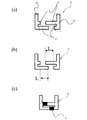
図3は、本実施形態において、導電部材上にバイパスダイオードを固定する状況を示しており、(a)は導電部材上にバイパスダイオードを固定する状況を説明するための概略図、(b)は導電部材上にバイパスダイオードを固定する状態を説明するための概略図である。図3において、5はバイパスダイオード、2は導電部材、9はバイパスパスダイオードの電極である。 FIG. 3 shows a situation in which the bypass diode is fixed on the conductive member in this embodiment, (a) is a schematic diagram for explaining the situation in which the bypass diode is fixed on the conductive member, and (b) It is the schematic for demonstrating the state which fixes a bypass diode on an electrically-conductive member. In FIG. 3, 5 is a bypass diode, 2 is a conductive member, and 9 is an electrode of the bypass pass diode.
図示するように、導電部材2上にバイパスダイオード5の電極9を位置合わせして、電気接続する。この電気接続には、一般的には半田付けを用いる。
As shown in the drawing, the electrode 9 of the
一方、ダイオードには定格電流がある。ダイオード毎に接合温度の上限設定があり、この接合温度以下で使用しなければならない。定格電流以上が流れると、接合温度以上となってしまい、ダイオードが破壊する虞れがある。したがってダイオードは定格電流を増大させるために接合部の面積を増大させる。すなわち、ダイオード素子を並列に大面積で構成する必要がある。そのため、定格電流が大きくなるとダイオードの体積は大きくなってしまう。 On the other hand, a diode has a rated current. Each diode has an upper limit for the junction temperature, and must be used below this junction temperature. If the current exceeds the rated current, the temperature will be higher than the junction temperature and the diode may be destroyed. Thus, the diode increases the junction area to increase the rated current. That is, it is necessary to configure the diode elements in large areas in parallel. Therefore, when the rated current increases, the volume of the diode increases.
光起電力素子1を流れる電流がダイオードの定格電流以上となった場合、定格電流の大きなダイオードを使用するのではなく、定格電流の小さな複数個のバイパスダイオード5を並列に形成することで、光起電力素子1の一体封止時における脱気性、封止性を改善することができる。
When the current flowing through the
〔導電部材〕
本実施形態における導電部材2は、バイパスダイオード5と光起電力素子1の正負電極間を電気的に接続する配線部材である。封止材中への封止性を良くするために銅箔を使用することが多いが、特に限定されない。バイパスダイオード5の光起電力素子1への電気接続は、予めバイパスダイオード5と導電部材2とを一体にしておいてから、光起電力素子1と電気的に接続する。バイパスダイオード5のアノード極、カソード極に配置される導電部材2は、バイパスダイオード5を互い違いに位置をずらして千鳥状に配置できるような形状に作成されていると都合が良い。
[Conductive member]
The
図4、本実施形態において、バイパスダイオードと導電部材とを一体形成する状況を示しており、(a)は導電部材を説明するための概略図、(b)は導電部材のバイパスダイオード側接続部の長さを説明するための概略図、(c)はダイオードと導電部材が一体形成された状態を表す概略図である。図4において、2は導電部材、5はバイパスダイオード、10は導電部材の光起電力素子側接続部、11は導電部材のバイパスダイオード側接続部である。 FIG. 4 shows a state in which the bypass diode and the conductive member are integrally formed in the present embodiment, wherein (a) is a schematic diagram for explaining the conductive member, and (b) is a bypass diode side connection portion of the conductive member. Schematic for demonstrating the length of this, (c) is the schematic showing the state by which the diode and the electrically-conductive member were integrally formed. In FIG. 4, 2 is a conductive member, 5 is a bypass diode, 10 is a photovoltaic element side connection part of the conductive member, and 11 is a bypass diode side connection part of the conductive member.
図示するように、導電部材2は、一対の光起電力素子側接続部10と2系統のバイパスダイオード側接続部11とから成り、これらバイパスダイオード側接続部11は上記光起電力素子接続部10、10間に並列に配されている。導電部材2のバイパスダイオード側接続部11に長さの違いLをつけることで、バイパスダイオード5を互い違いに位置をずらして千鳥状に配置することができる。例えば、Lの長さをバイパスダイオード5の長さ以上とすることで、互い違いに位置をずらした千鳥状配置とすることができる。バイパスダイオード5と導電部材2との電気接続は、上述したように、例えば半田付けして接続する。
As shown in the drawing, the
〔バイパスダイオードの配置〕
本発明におけるバイパスダイオード5の千鳥状配置とは、一つの光起電力素子に並列接続する一群のバイパスダイオードの配置が、光起電力素子受光面側から見ると互い違いに位置がずれてジグザクに点在している状態をいう。
[Placement of bypass diode]
The zigzag arrangement of the
このような状態を実現するには、導電部材2のバイパスダイオード側接続部11の一端からの長さが、隣接する並走するバイパスダイオード側接続部の一端からの長さと異なるようにすることで実現できる。
In order to realize such a state, the length of the
なお、前述した導電部材2の長さの差Lは、バイパスダイオード自体の並走方向に沿っている長さよりも、大きい方が好ましい。特に、バイパスダイオード5が矩形状である場合は、最も隣接するバイパスダイオード間の最近接距離が、バイパスダイオード5の頂点間の距離であるような状態が好ましい。
The length difference L of the
また、複数の光起電力素子1を直列または並列に電気的に接続して光起電力素子群を構成する場合、光起電力素子間には間隔が設けるが、この間隔及びその延長線上の領域にはバイパスダイオード5が存在しないことが好ましい。光起電力素子間の間隔及びその延長線上の領域にバイパスダイオード5が存在しないことにより、光起電力素子間での太陽電池モジュールの屈曲があった場合にその応力がバイパスダイオード5に及ばないため、バイパスダイオード5が破損するなどのトラブル発生を防止することができる。
Further, when a plurality of
以上のように、本実施形態の太陽電池モジュールによれば、複数の光起電力素子1を直列または並列に電気的に接続して光起電力素子群を構成した場合に、隣接する光起電力素子同士を導電部材2が跨ぐように形成されているので、光起電力素子群のうちのいずれかの光起電力素子1が影となっても、影となった光起電力素子1に逆方向の電圧が印加されるのを防止することができる。
As described above, according to the solar cell module of the present embodiment, when a plurality of
また、光起電力素子1に容量の小さな複数のバイパスダイオード5を並列接続しても、隣接する導電部材2上におけるバイパスダイオード5の配置を互い違いに千鳥状とすることにより、封止材6の使用量を削減することができる。
Further, even when a plurality of
さらに、隣接する導電部材2上におけるバイパスダイオード5の配置を互い違いに千鳥状とすることにより、バイパスダイオード5の近傍での脱気が促されて、封止する部材間への封止材6の流れ込みがスムーズになり、バイパスダイオード5の近傍に気泡が残らないように封止できる。これにより、太陽電池モジュールの外観が良好となるだけでなく、屋外長期使用における太陽電池モジュールの信頼性を向上させることができる。
Furthermore, by alternately arranging the
以下、本発明の好適な実施例に詳細に説明するが、本発明はこれらの実施例に限定されるものではない。 Hereinafter, although the preferred examples of the present invention are described in detail, the present invention is not limited to these examples.
〔実施例1〕
実施例1の太陽電池モジュールは、光起電力素子に2個のバイパスダイオード5が並列に電気接続されており、被覆材が表面側、裏面側共に耐候性フィルムで構成されているものである。
[Example 1]
In the solar cell module of Example 1, two
図5は、実施例1で使用する光起電力素子の断面構成を示す模式図である。図5において、1は光起電力素子、21は導電性基体、22は金属電極層、23は半導体光活性層、24は透明導電層、25は集電電極、26は正極電極材である。 FIG. 5 is a schematic diagram showing a cross-sectional configuration of the photovoltaic element used in Example 1. In FIG. 5, 1 is a photovoltaic element, 21 is a conductive substrate, 22 is a metal electrode layer, 23 is a semiconductor photoactive layer, 24 is a transparent conductive layer, 25 is a collecting electrode, and 26 is a positive electrode material.
図示するように、本実施例における光起電力素子1は、導電性基体21としてステンレス鋼板を使用し、その上に裏面側の金属電極層22としてAl層とZnO層を順次形成する。その上に、n型a−Si層、i型a−Si層、p型微結晶μc−Si層を形成し、a−Si系半導体光活性層23を形成する。そして、透明導電層24としてIn2O3薄膜を形成する。次に、銀ペーストからなる集電電極25をスクリーン印刷後、乾燥して形成し、最後に正極電極材26を光起電力素子1の端部に形成して、光起電力素子1を作製する。
As shown in the figure, the
以上のようにして、大きさが240mm×360mmの光起電力素子1を作製する。光起電力素子1の一枚当たりの定格電流は10Aである。
As described above, the
次に、バイパスダイオードと導電部材を一体化する。図4に示したように、バイパスダイオード5は定格5A品(寸法が幅2.5mm、長さ4mm)を2個使用する。導電部材2は、厚さ0.1mmt、幅2.5mmの銅箔で、図4のような形状に切断されたものを準備しておき、半田付けしてバイパスダイオード5と一体にする。図4中のLは導電部材2のバイパスダイオード側接続部11の長さ違いであり、本実施例では8mmとする。各バイパスダイオード5の長さが4mmであるため、これらを互い違いに位置ずれするように千鳥状に配置することができる。
Next, the bypass diode and the conductive member are integrated. As shown in FIG. 4, two
そして、バイパスダイオード5を固定した導電部材2を光起電力素子1へ電気的に接続する。図1及び図4に示したように、導電部材2の光起電力素子側接続部10うちの一方は正極電極材32上に、他方は不図示の導電性基材上に電気的に接続する。このとき、光起電力素子1の端部から最も離れたバイパスダイオード5の外側端部までの距離dが8mmとなるように電気接続する。また、バイパスダイオード5のカソード側の導電部材2が光起電力素子1の正極電極材側に接続されるように注意する。
Then, the
次に、図2に示したように、上記のように作製した光起電力素子1を封止する。本実施例では、封止材6としてEVAを、表面被覆材7としてフッ素樹脂フィルムを、裏面被覆材8としてポリエステルフィルムを使用する。各被覆材料の大きさは270mm×380mmとしている。図2のように、裏面被覆材8、封止材6、上記のように作製した光起電力素子1、封止材6、表面被覆材7の順に積層し、これらの部材間を真空引きすると共に加熱処理して封止する。
Next, as shown in FIG. 2, the
図6は、実施例1で作製した封止後の太陽電池モジュールの断面構造を示す概略図である。図6において、1は光起電力素子、5はバイパスダイオード、6は封止材、7は表面被覆材、8は裏面被覆材である。封止後の太陽電池モジュールは、気泡残りがなく、外観仕上がりの良好なものであった。 6 is a schematic view showing a cross-sectional structure of the sealed solar cell module produced in Example 1. FIG. In FIG. 6, 1 is a photovoltaic element, 5 is a bypass diode, 6 is a sealing material, 7 is a surface coating material, and 8 is a back surface coating material. The sealed solar cell module had no bubbles remaining and had a good appearance.
以上のように、隣接する導電部材2上のバイパスダイオード5を互い違いに位置をずらして千鳥状に配置することで、一体成形時に脱気が促されて封止材6の流れ込みがスムーズとなり、気泡残りがないように封止できる。これにより、太陽電池モジュールの外観が良好になるだけでなく、屋外長期使用における太陽電池モジュールの信頼性を向上させることができる。
As described above, the
〔実施例2〕
実施例2の太陽電池モジュールは、光起電力素子に3個のバイパスダイオード5が並列に電気接続されており、被覆材の表面側にガラス、裏面側はフィルムで構成されているものである。
[Example 2]
In the solar cell module of Example 2, three
図7は、実施例2で使用するバイパスダイオードと導電部材とを一体形成する状況を示しており、(a)は導電部材を説明するための概略図、(b)は導電部材のバイパスダイオード側接続部の長さを説明するための概略図、(c)はダイオードと導電部材とが一体になった状態を表す概略図である。図7において、2は導電部材、5はバイパスダイオード、10は導電部材の光起電力素子側接続部、11は導電部材のバイパスダイオード側接続部である。 FIG. 7 shows a situation in which the bypass diode and the conductive member used in Example 2 are integrally formed. (A) is a schematic diagram for explaining the conductive member, and (b) is a bypass diode side of the conductive member. Schematic for demonstrating the length of a connection part, (c) is the schematic showing the state with which the diode and the electrically-conductive member were united. In FIG. 7, 2 is a conductive member, 5 is a bypass diode, 10 is a photovoltaic element side connection part of the conductive member, and 11 is a bypass diode side connection part of the conductive member.
本実施例で使用するバイパスダイオード5は、定格電流3.5A品(寸法が幅2.0mm、長さ3mm)を使用する。導電部材2は、厚さ0.1mmt、幅2.0mmの銅箔で、図7のような形状に切断されたものを準備しておき、半田付けしてバイパスダイオード5と一体にする。図7中のLは、導電部材2のバイパスダイオード側接続部11の長さ違いであり、本実施例では6mmとする。各バイパスダイオード5の長さが3mmであるため、これらを互い違いに位置ずれするように千鳥状に配置することができる。
The
次に、バイパスダイオード5を固定した導電部材2を光起電力素子1へ電気的に接続する。光起電力素子1は実施例1のようにして作製したものを使用する。
Next, the
図8は、実施例2で使用する光起電力素子を示す概略図である。図8において、1は光起電力素子、2は導電部材、3は正極電極材、5はバイパスダイオードである。 FIG. 8 is a schematic view showing a photovoltaic element used in Example 2. In FIG. 8, 1 is a photovoltaic element, 2 is a conductive member, 3 is a positive electrode material, and 5 is a bypass diode.
図示するように、導電部材2の光起電力素子側接続部10うちの一方は正極電極材3上に、他方は不図示の導電性基材上に電気的に接続する。このとき、光起電力素子1の端部から最も離れたバイパスダイオード5の外側端部までの距離dが12mmとなるように電気接続する。また、バイパスダイオード5のカソード側の導電部材2が光起電力素子1の正極電極材側に接続されるように注意する。
As shown in the drawing, one of the photovoltaic element
次に、上記のように作製した光起電力素子1を封止する。本実施例では、表面被覆材7としてガラス板を使用する以外は、実施例1と同じ材料を使用している。各被覆材料の大きさは275mm×380mmとしている。図2のように、裏面被覆材8、封止材6、上記のように作製した光起電力素子1、封止材6、表面被覆材7の順に積層し、これらの部材間を真空引きすると共に加熱処理して封止する。
Next, the
以上のように、3個のバイパスダイオード5が並列接続されている場合でも、実施例1と同様に、各バイパスダイオード5を互い違いに位置ずれするように千鳥状に配置することで、気泡残りがなく、外観仕上がりの良好な太陽電池モジュールを作製することができる。
As described above, even when the three
〔実施例3〕
実施例3の太陽電池モジュールは、複数の光起電力素子を直列に電気接続して光起電力素子群を形成し、バイパスダイオード5を並列配置する導電部材は光起電力素子間に跨るように配して作製し、光起電力素子群を一体封止後、その周囲に枠材を取り付けたものである。
Example 3
In the solar cell module of Example 3, a plurality of photovoltaic elements are electrically connected in series to form a photovoltaic element group, and the conductive member in which the
図9は実施例3の光起電力素子の直列接続部を示す概略図、図10は図9のバイパスダイオード配置部を示す拡大概略図である。これらの図において、1は光起電力素子、2は導電部材、5はバイパスダイオード、12は光起電力素子間の間隔の延長線上の領域である。 FIG. 9 is a schematic view showing a series connection portion of the photovoltaic elements of Example 3, and FIG. 10 is an enlarged schematic view showing the bypass diode arrangement portion of FIG. In these drawings, 1 is a photovoltaic element, 2 is a conductive member, 5 is a bypass diode, and 12 is a region on an extension line of the interval between the photovoltaic elements.
図示するように、二枚の光起電力素子1を直列接続しており、これら光起電力素子間の間隔の延長線上の領域403に跨るように、導電部材2上に2個のバイパスダイオード5を並列接続して配置している。光起電力素子間の隙間は5mmとしている。
As shown in the figure, two
使用したダイオードは実施例1と同じであり、導電部材2のバイパスダイオード側接続部11の長さ違いL(図4のL)は12mmとしている。こうすることで、図10に示すように、光起電力素子間の間隔の延長線上の領域12にバイパスダイオード5が存在しないように配置できる。また、本実施例における光起電力素子1において、不図示の導電性基体は負極電極を兼ねているので、アノード側、カソード側の双方の導電部材2は、光起電力素子1の導電性基体に直接電気接続されている。さらに、光起電力素子1の端部から最も離れているバイパスダイオード5の外側端部までの距離dは、実施例1と同じく8mmとしている。
The used diode is the same as in Example 1, and the length difference L (L in FIG. 4) of the bypass diode
次に、上述したような要領で、複数の光起電力素子1を直列接続して光起電力素子群を形成し、大面積の太陽電池モジュールを作製する。
Next, in the manner described above, a plurality of
図11は、実施例3の太陽電池モジュールを作製する状況を示しており、(a)は複数の光起電力素子を直列化した状態を説明する概略図、(b)は一体封止後に枠材を取り付けた状態を表す概略図である。図11において、1は光起電力素子、13は光起電力素子間の間隔、14は枠材、15は直列化Uターン部の渡し電極、16は正極電極の延長部である。 FIG. 11 shows a situation in which the solar cell module of Example 3 is manufactured, (a) is a schematic diagram illustrating a state in which a plurality of photovoltaic elements are serialized, and (b) is a frame after integral sealing. It is the schematic showing the state which attached the material. In FIG. 11, 1 is a photovoltaic element, 13 is a space between photovoltaic elements, 14 is a frame member, 15 is a transfer electrode of a serialized U-turn part, and 16 is an extension part of a positive electrode.
図11(a)に示すように、4枚の光起電力素子1を直列接続して1列の直列体を形成し、これを2列作製して並列に配置し、Uターンするように2列の直列体を直列接続する。また、直列化Uターン部では渡し電極15を使用して2列の光起電力素子群を直列化し、直列化の端部では正極電極を延長して、この延長部16と導電性基体との間にバイパスダイオード5を電気的に接続している。このようにして各光起電力素子1にバイパスダイオード5を接続する。
As shown in FIG. 11 (a), four
次に、複数の光起電力素子1の直列化して光起電力素子群を形成後、その封止工程を行う。各被覆材料の大きさは、505mm×1475mmとしている。被覆材料の寸法変更以外は、実施例1と同様にして作製する。
Next, after a plurality of
最後に、図11(b)に示すように、光起電力素子群の周囲に枠材14を取り付けて、太陽電池モジュールを作製する。
Finally, as shown in FIG.11 (b), the
以上のように、複数の光起電力素子1を直列化して光起電力素子群を形成した場合においては、バイパスダイオード5を光起電力素子間の間隔13に跨って配置できる。また、バイパスダイオード5が光起電力素子間の間隔13の延長線上の領域12に存在しないように配置することで、光起電力素子間での太陽電池モジュールの屈曲があった場合にその応力がバイパスダイオード5に及ばないため、バイパスダイオード5が破損するなどのトラブル発生を防止することができる。
As described above, when a plurality of
本実施例では、バイパスダイオード5は、図11に示すように、光起電力素子1の一端側にのみ設けてあるので、各直列体は互いにバイパスダイオード5が形成されていない側を突き合わせて配置することで、並走する2列の直列体間の間隔を最小に設定することができる。また、以上のような構成とすることで、太陽電池モジュールが枠材14により遮光される領域に各バイパスダイオード5を配置することができる。通常、太陽電池モジュールと枠材14との間には、このような枠材14により遮光される領域は必ず必要である。さらに、上記のように複数列の直列体をUターンするように直列接続して大面積の太陽電池モジュールを形成する場合において、封止材の使用量を大幅に削減することが可能となるものである。
In this embodiment, as shown in FIG. 11, the
1 光起電力素子
2 導電部材
3 光起電力素子の正極電極材
4 光起電力素子の集電電極
5 バイパスダイオード
6 封止材
7 表面被覆材
8 裏面被覆材
9 バイパスパスダイオードの電極
10 導電部材の光起電力素子側接続部
11 導電部材のバイパスダイオード側接続部
12 光起電力素子間の間隔の延長線上の領域
13 光起電力素子間の間隔
14 枠材
15 直列化Uターン部の渡し電極
16 正極電極の延長部
21 導電性基体
22 金属電極層
23 半導体光活性層
24 透明導電層
25 集電電極
26 正極電極材
DESCRIPTION OF
Claims (3)
上記導電部材は、対の光起電力素子側接続部と複数系統のバイパスダイオード側接続部とから構成され、これらバイパスダイオード側接続部は上記光起電力素子接続部間に並列に配されており、隣接する系統のバイパスダイオード側接続部上に各バイパスダイオードが互い違いに位置をずらして配置されていることを特徴とする太陽電池モジュール。 In a solar cell module having at least one photovoltaic element, a bypass diode for preventing reverse voltage application of the photovoltaic element, and a conductive member for disposing the bypass diode,
The conductive member is composed of a pair of photovoltaic element side connection parts and a plurality of bypass diode side connection parts, and these bypass diode side connection parts are arranged in parallel between the photovoltaic element connection parts. A solar cell module, wherein the bypass diodes are alternately arranged on the bypass diode side connection portions of adjacent systems.
The solar cell module according to claim 2, wherein a space is provided between the photovoltaic elements, and the bypass diode does not exist in the space and a region on an extension line thereof.
Priority Applications (2)
| Application Number | Priority Date | Filing Date | Title |
|---|---|---|---|
| JP2003422103A JP2005183660A (en) | 2003-12-19 | 2003-12-19 | Solar cell module |
| US11/009,004 US20050133086A1 (en) | 2003-12-19 | 2004-12-13 | Solar cell module with conductor member and with bypass diode arranged on condcutor member, and method of producing same |
Applications Claiming Priority (1)
| Application Number | Priority Date | Filing Date | Title |
|---|---|---|---|
| JP2003422103A JP2005183660A (en) | 2003-12-19 | 2003-12-19 | Solar cell module |
Publications (1)
| Publication Number | Publication Date |
|---|---|
| JP2005183660A true JP2005183660A (en) | 2005-07-07 |
Family
ID=34675304
Family Applications (1)
| Application Number | Title | Priority Date | Filing Date |
|---|---|---|---|
| JP2003422103A Withdrawn JP2005183660A (en) | 2003-12-19 | 2003-12-19 | Solar cell module |
Country Status (2)
| Country | Link |
|---|---|
| US (1) | US20050133086A1 (en) |
| JP (1) | JP2005183660A (en) |
Cited By (2)
| Publication number | Priority date | Publication date | Assignee | Title |
|---|---|---|---|---|
| JP2008512860A (en) * | 2004-09-11 | 2008-04-24 | アズール・スペース・ソーラー・パワー・ゲーエムベーハー | Solar cell assembly and method for connecting solar cell strings |
| TWI552358B (en) * | 2011-10-11 | 2016-10-01 | 林世賢 | A diode unit module used in a solar photovoltaic system including a solar photovoltaic template |
Families Citing this family (16)
| Publication number | Priority date | Publication date | Assignee | Title |
|---|---|---|---|---|
| JP2005175197A (en) * | 2003-12-11 | 2005-06-30 | Canon Inc | Solar cell module and manufacturing method thereof |
| US20050224109A1 (en) * | 2004-04-09 | 2005-10-13 | Posbic Jean P | Enhanced function photovoltaic modules |
| US20080257402A1 (en) * | 2005-10-21 | 2008-10-23 | Michael Viktor Kamp | Solar Power System with a Number of Photovoltaic Modules |
| WO2009002350A1 (en) * | 2006-07-10 | 2008-12-31 | Scott Frazier | Solar energy conversion devices and systems |
| US20080302031A1 (en) * | 2007-06-05 | 2008-12-11 | Solar Roofing Systems, Inc., | Integrated solar roofing tile connection system |
| JP5497037B2 (en) * | 2008-08-06 | 2014-05-21 | エムビーシー・ベンチャーズ・インコーポレイテッド | Solar energy conversion |
| US9018519B1 (en) | 2009-03-10 | 2015-04-28 | Solaero Technologies Corp. | Inverted metamorphic multijunction solar cells having a permanent supporting substrate |
| US20100229933A1 (en) * | 2009-03-10 | 2010-09-16 | Emcore Solar Power, Inc. | Inverted Metamorphic Multijunction Solar Cells with a Supporting Coating |
| US20110108084A1 (en) * | 2009-10-25 | 2011-05-12 | Tisler Anthony C | In-line flexible diode assembly for use in photovoltaic modules and method of making the same |
| EP2352178A1 (en) * | 2010-01-29 | 2011-08-03 | Saint-Gobain Glass France | Solar module assemblies and diode cable |
| US8563849B2 (en) * | 2010-08-03 | 2013-10-22 | Sunpower Corporation | Diode and heat spreader for solar module |
| US8581242B2 (en) * | 2012-02-21 | 2013-11-12 | Atomic Energy Council—Institute of Nuclear Energy Research | Apparatus combining bypass diode and wire |
| WO2014047457A2 (en) | 2012-09-20 | 2014-03-27 | Mbc Ventures, Inc. | Controller for skylight energy management system |
| US9627565B2 (en) * | 2013-11-27 | 2017-04-18 | Space Systems/Loral, Llc | Integral corner bypass diode interconnecting configuration for multiple solar cells |
| CN111584473B (en) * | 2020-06-08 | 2023-09-01 | 无锡尚德太阳能电力有限公司 | Dual-chip diode module |
| DE102023000609A1 (en) * | 2023-02-21 | 2024-08-22 | Azur Space Solar Power Gmbh | Protection of space solar cells in a string arrangement |
Family Cites Families (53)
| Publication number | Priority date | Publication date | Assignee | Title |
|---|---|---|---|---|
| JP3170105B2 (en) * | 1993-07-01 | 2001-05-28 | キヤノン株式会社 | Solar cell module |
| US5589006A (en) * | 1993-11-30 | 1996-12-31 | Canon Kabushiki Kaisha | Solar battery module and passive solar system using same |
| JPH07302926A (en) * | 1994-04-30 | 1995-11-14 | Canon Inc | Solar cell module |
| JP3618802B2 (en) * | 1994-11-04 | 2005-02-09 | キヤノン株式会社 | Solar cell module |
| JP2915327B2 (en) * | 1995-07-19 | 1999-07-05 | キヤノン株式会社 | Solar cell module and method of manufacturing the same |
| CN1169228C (en) * | 1995-08-24 | 2004-09-29 | 佳能株式会社 | Solar cell module, its manufacturing method and building element |
| US5616185A (en) * | 1995-10-10 | 1997-04-01 | Hughes Aircraft Company | Solar cell with integrated bypass diode and method |
| JPH10112549A (en) * | 1996-10-08 | 1998-04-28 | Canon Inc | Solar cell module |
| JPH10209474A (en) * | 1997-01-21 | 1998-08-07 | Canon Inc | Solar cell module and method of manufacturing the same |
| JPH10233521A (en) * | 1997-02-19 | 1998-09-02 | Canon Inc | Solar cell module, solar cell integrated building material using the same, and solar power generation device |
| US5998729A (en) * | 1997-04-11 | 1999-12-07 | Canon Kabushiki Kaisha | Solar cell module having improved flexibility |
| JPH11135820A (en) * | 1997-08-27 | 1999-05-21 | Canon Inc | Solar cell module and reinforcing member for solar cell module |
| JPH11150287A (en) * | 1997-09-10 | 1999-06-02 | Canon Inc | Solar cell module, enclosure with solar cell, method of installing enclosure with solar cell, and solar power generation system |
| JP3397659B2 (en) * | 1997-10-30 | 2003-04-21 | キヤノン株式会社 | Photovoltaic roof and construction method |
| JP3792867B2 (en) * | 1997-11-06 | 2006-07-05 | キヤノン株式会社 | Solar cell module, solar cell array, and solar power generation apparatus construction method |
| JP3586083B2 (en) * | 1997-11-13 | 2004-11-10 | キヤノン株式会社 | Arrangement method of solar cell module and solar cell module array |
| JPH11193612A (en) * | 1997-12-27 | 1999-07-21 | Canon Inc | Mounting method of fixing member, solar cell module array, solar cell power generation system and solar cell module or exterior material |
| JPH11289103A (en) * | 1998-02-05 | 1999-10-19 | Canon Inc | Semiconductor device, solar cell module and disassembly method thereof |
| IT1298560B1 (en) * | 1998-02-05 | 2000-01-12 | Sgs Thomson Microelectronics | CURRENT GENERATOR VERY STABLE IN TEMPERATURE |
| JPH11238897A (en) * | 1998-02-23 | 1999-08-31 | Canon Inc | Solar cell module manufacturing method and solar cell module |
| JP3675218B2 (en) * | 1998-04-06 | 2005-07-27 | キヤノン株式会社 | SOLAR CELL MODULE, ITS CONSTRUCTION METHOD, AND POWER GENERATION DEVICE USING THE SOLAR CELL MODULE |
| US6175075B1 (en) * | 1998-04-21 | 2001-01-16 | Canon Kabushiki Kaisha | Solar cell module excelling in reliability |
| EP0962989B1 (en) * | 1998-05-20 | 2011-01-19 | Canon Kabushiki Kaisha | Photovoltaic power generating structure |
| JP2000286437A (en) * | 1998-06-12 | 2000-10-13 | Canon Inc | Solar cell module and manufacturing method |
| JP2000200919A (en) * | 1998-10-30 | 2000-07-18 | Canon Inc | Solar cell module and solar cell array |
| JP2000243995A (en) * | 1998-12-25 | 2000-09-08 | Canon Inc | Inspection method and manufacturing method of solar cell module |
| US6291761B1 (en) * | 1998-12-28 | 2001-09-18 | Canon Kabushiki Kaisha | Solar cell module, production method and installation method therefor and photovoltaic power generation system |
| JP2000269535A (en) * | 1999-01-14 | 2000-09-29 | Canon Inc | Solar cell module, power generation device, method for separating solar cell module, and method for regenerating solar cell module |
| JP2000312019A (en) * | 1999-02-25 | 2000-11-07 | Canon Inc | Photovoltaic module array, photovoltaic module array installation structure, photovoltaic module installation method, and photovoltaic power generation system |
| JP2000345675A (en) * | 1999-03-26 | 2000-12-12 | Canon Inc | Solar cell module, roof with solar cell, and solar cell power generation system |
| US6414236B1 (en) * | 1999-06-30 | 2002-07-02 | Canon Kabushiki Kaisha | Solar cell module |
| US6635507B1 (en) * | 1999-07-14 | 2003-10-21 | Hughes Electronics Corporation | Monolithic bypass-diode and solar-cell string assembly |
| JP4336442B2 (en) * | 2000-05-23 | 2009-09-30 | キヤノン株式会社 | Solar cell module |
| AU5400501A (en) * | 2000-06-27 | 2002-01-03 | Canon Kabushiki Kaisha | Photovoltaic element, producing method therefor, and solar cell modules |
| JP2002083990A (en) * | 2000-07-06 | 2002-03-22 | Canon Inc | Photovoltaic element assembly, solar cell module using the same, and method of manufacturing solar cell module |
| US6653549B2 (en) * | 2000-07-10 | 2003-11-25 | Canon Kabushiki Kaisha | Photovoltaic power generation systems and methods of controlling photovoltaic power generation systems |
| US6806415B2 (en) * | 2000-11-10 | 2004-10-19 | Canon Kabushiki Kaisha | Method for controlling a solar power generation system having a cooling mechanism |
| JP2002198555A (en) * | 2000-12-26 | 2002-07-12 | Canon Inc | Semiconductor element mounting substrate and semiconductor device using the substrate |
| JP2003031829A (en) * | 2001-05-09 | 2003-01-31 | Canon Inc | Photovoltaic element |
| JP2002359048A (en) * | 2001-05-31 | 2002-12-13 | Canon Inc | Conductor connection method, conductor connection structure, and solar cell module having the connection structure |
| JP2002359386A (en) * | 2001-05-31 | 2002-12-13 | Canon Inc | Solar cell string, solar cell array and solar power generation system |
| JP2002359387A (en) * | 2001-06-01 | 2002-12-13 | Canon Inc | Solar cell installation structure and solar power generation system |
| JP2002368247A (en) * | 2001-06-01 | 2002-12-20 | Canon Inc | Solar cell structure, solar cell array, and solar power generation system |
| JP2003158282A (en) * | 2001-08-30 | 2003-05-30 | Canon Inc | Solar power system |
| JP2004006702A (en) * | 2002-03-28 | 2004-01-08 | Canon Inc | Solar cell module placement structure, solar cell module array, and solar energy power generation system |
| JP3744458B2 (en) * | 2002-04-10 | 2006-02-08 | 住友電装株式会社 | Terminal box device for solar cell module |
| JP4401649B2 (en) * | 2002-12-13 | 2010-01-20 | キヤノン株式会社 | Manufacturing method of solar cell module |
| JP2004288898A (en) * | 2003-03-24 | 2004-10-14 | Canon Inc | Method of manufacturing solar cell module |
| US7534956B2 (en) * | 2003-04-10 | 2009-05-19 | Canon Kabushiki Kaisha | Solar cell module having an electric device |
| JP2004319800A (en) * | 2003-04-17 | 2004-11-11 | Canon Inc | Solar cell module |
| JP2004319812A (en) * | 2003-04-17 | 2004-11-11 | Canon Inc | Solar cell module with power converter |
| JP2005150318A (en) * | 2003-11-14 | 2005-06-09 | Canon Inc | Solar cell module and manufacturing method thereof |
| JP2005175197A (en) * | 2003-12-11 | 2005-06-30 | Canon Inc | Solar cell module and manufacturing method thereof |
-
2003
- 2003-12-19 JP JP2003422103A patent/JP2005183660A/en not_active Withdrawn
-
2004
- 2004-12-13 US US11/009,004 patent/US20050133086A1/en not_active Abandoned
Cited By (2)
| Publication number | Priority date | Publication date | Assignee | Title |
|---|---|---|---|---|
| JP2008512860A (en) * | 2004-09-11 | 2008-04-24 | アズール・スペース・ソーラー・パワー・ゲーエムベーハー | Solar cell assembly and method for connecting solar cell strings |
| TWI552358B (en) * | 2011-10-11 | 2016-10-01 | 林世賢 | A diode unit module used in a solar photovoltaic system including a solar photovoltaic template |
Also Published As
| Publication number | Publication date |
|---|---|
| US20050133086A1 (en) | 2005-06-23 |
Similar Documents
| Publication | Publication Date | Title |
|---|---|---|
| CN101779297B (en) | Solar cell module | |
| US9515214B2 (en) | Solar battery module and manufacturing method thereof | |
| CN105874609B (en) | The modular manufacture of solar energy battery core with low resistance electrode | |
| US8927850B2 (en) | Photovoltaic module | |
| KR101554045B1 (en) | Solar cell module | |
| KR101679452B1 (en) | Solar battery, solar battery module and solar battery system | |
| JP2005183660A (en) | Solar cell module | |
| US8497419B2 (en) | Solar cell module | |
| JP5714080B2 (en) | Solar cell module | |
| JP2005011869A (en) | Solar cell module and its manufacturing method | |
| TW201601328A (en) | Photovoltaic module | |
| JP5328996B2 (en) | SOLAR BATTERY CELL, SOLAR BATTERY MODULE AND SOLAR CELL LEAD JOIN | |
| JP2012019094A (en) | Solar cell module | |
| US9153713B2 (en) | Solar cell modules and methods of manufacturing the same | |
| JP2012129359A (en) | Solar cell module and solar cell | |
| JP5637089B2 (en) | Solar cell module | |
| JP2010238938A (en) | Solar cell, solar cell module, and solar cell system | |
| KR101192345B1 (en) | Pattern Of The Electrode Of Solar Cell And Sollar Cell Comprising The Said Electrode Pattern | |
| JPH0567017U (en) | Solar cell module | |
| JP5485434B1 (en) | Solar cells | |
| JP2005167161A (en) | Method of manufacturing solar battery module | |
| KR102410785B1 (en) | Shingled high power module and manufacturing method thereof | |
| CN111868936A (en) | Solar cell modules and solar power generation systems | |
| JP5367090B2 (en) | Solar cell module and manufacturing method thereof | |
| JP2002190611A (en) | Power generation device with multiple solar cell modules |
Legal Events
| Date | Code | Title | Description |
|---|---|---|---|
| A300 | Application deemed to be withdrawn because no request for examination was validly filed |
Free format text: JAPANESE INTERMEDIATE CODE: A300 Effective date: 20070306 |