JP2005032785A - Method of manufacturing semiconductor device - Google Patents
Method of manufacturing semiconductor device Download PDFInfo
- Publication number
- JP2005032785A JP2005032785A JP2003193297A JP2003193297A JP2005032785A JP 2005032785 A JP2005032785 A JP 2005032785A JP 2003193297 A JP2003193297 A JP 2003193297A JP 2003193297 A JP2003193297 A JP 2003193297A JP 2005032785 A JP2005032785 A JP 2005032785A
- Authority
- JP
- Japan
- Prior art keywords
- film
- insulating film
- semiconductor substrate
- semiconductor device
- material film
- Prior art date
- Legal status (The legal status is an assumption and is not a legal conclusion. Google has not performed a legal analysis and makes no representation as to the accuracy of the status listed.)
- Pending
Links
Images


Landscapes
- Testing Or Measuring Of Semiconductors Or The Like (AREA)
- Drying Of Semiconductors (AREA)
- Internal Circuitry In Semiconductor Integrated Circuit Devices (AREA)
Abstract
Description
【0001】
【発明の属する技術分野】
本発明は、半導体装置の製造技術に関し、特に、層間絶縁膜の半導体基板面内での膜厚均一化に適用して有効な技術に関する。
【0002】
【従来の技術】
半導体基板にMISFETなどの半導体素子を形成した後、半導体基板上に層間絶縁膜を形成する。形成された層間絶縁膜は、その上面を平坦化するためにCMP処理される。
【0003】
特開2002−299256号公報には、被処理基板上の成膜の膜厚分布の不均一性を解消するために、複数の反応ガス導入用の穴が設けられ、被処理基板の表面に向かい合うように配置したシャワーヘッドを有する半導体製造装置において、被処理基板の中心に1番近い第1の円周上にある第1の穴からガスの流量Aが吹き出され、第1の円周の外側にある第2の円周上の第2の穴の位置までに、ガスが反応してガスの流量が流量Aから、流量A−流量Bとなり、流量A−流量Bとなったガスの流量を流量Aに戻すため、第2の円周上の第2の穴の位置で、流量Bを足し、このように穴のある各円周上で流量をAに戻すことにより、被処理基板面内でのガスの流量が略変わらないようにした技術が記載されている(特許文献1参照)。
【0004】
【特許文献1】
特開2002−299256号公報
【0005】
【発明が解決しようとする課題】
本発明者の検討によれば、次のことが分かった。
【0006】
半導体基板上に層間絶縁膜などの材料膜を形成してCMP処理したとき、層間絶縁膜(材料膜)の上面は局所的には平坦化されるが、半導体基板の面内全体でみると、層間絶縁膜の上面にはうねり(ゆるやかな凹凸)が生じ、半導体基板面内での層間絶縁膜の膜厚分布が不均一になってしまう。このような現象は、半導体基板の直径が大きくなるほど顕著となる傾向にある。半導体基板面内での層間絶縁膜の膜厚分布が不均一であると、層間絶縁膜にスルーホールなどをドライエッチング法で形成する際に、層間絶縁膜が相対的に厚い領域ではスルーホールが非開口となる恐れがある。これを防止し、半導体基板面内のいずれの領域においてもスルーホールを確実に開口するには、ドライエッチング工程におけるオーバーエッチング量を比較的大きくする必要があるが、オーバーエッチングによるエッチングストッパ膜の突き抜けや半導体基板へのダメージなどを生じる恐れがある。これらは、半導体装置の製造歩留りを低下させる。このため、半導体基板面内での層間絶縁膜(材料膜)の膜厚分布をより均一にすることが好ましい。
【0007】
上記特許文献1には、被処理基板上の成膜の膜厚分布の不均一性を解消する成膜技術が記載されているが、成膜した段階で基板面内の膜厚分布が不均一となってしまった場合には対処できず、その半導体基板については半導体装置の製造歩留りが低下してしまう。
【0008】
本発明の目的は、半導体装置の製造歩留まりを向上できる半導体装置の製造方法を提供することにある。
【0009】
本発明の他の目的は、半導体基板上に形成した材料膜の半導体基板面内での膜厚分布の均一性を向上できる半導体装置の製造方法を提供することにある。
【0010】
本発明の前記ならびにその他の目的と新規な特徴は、本明細書の記述および添付図面から明らかになるであろう。
【0011】
【課題を解決するための手段】
本願において開示される発明のうち、代表的なものの概要を簡単に説明すれば、次のとおりである。
【0012】
本発明の半導体装置の製造方法は、半導体基板上に形成した第1材料膜の膜厚分布を測定し、測定した第1材料膜の膜厚分布に対応して選択した露光量分布で第1材料膜上に形成した第2感光性材料膜を露光処理し、現像処理後に残存する第2感光性材料膜と第1材料膜とをエッチングするものである。
【0013】
【発明の実施の形態】
以下、本発明の実施の形態を図面に基づいて詳細に説明する。なお、実施の形態を説明するための全図において、同一の機能を有する部材には同一の符号を付し、その繰り返しの説明は省略する。また、以下の実施の形態では、特に必要なとき以外は同一または同様な部分の説明を原則として繰り返さない。
【0014】
(実施の形態1)
本実施の形態の半導体装置の製造工程を図面を参照して説明する。図1〜図3は、本発明の一実施の形態である半導体装置、例えばMISFET(Metal Insulator Semiconductor Field Effect Transistor)、の製造工程中の要部断面図である。
【0015】
図1に示されるように、例えば1〜10Ωcm程度の比抵抗を有するp型の単結晶シリコンなどからなる半導体基板(半導体ウエハ)1が用意(準備)され、半導体基板1の主面に素子分離領域2が形成される。素子分離領域2は酸化シリコンなどからなり、例えばSTI(Shallow Trench Isolation)法またはLOCOS(Local Oxidization of Silicon )法などにより形成される。
【0016】
次に、半導体基板1のnチャネル型MISFETを形成する領域に、例えばホウ素(B)などの不純物をイオン注入することなどによってp型ウエル3を形成する。
【0017】
次に、p型ウエル3の表面にゲート絶縁膜4が形成される。ゲート絶縁膜4は、例えば薄い酸化シリコン膜などからなり、例えば熱酸化法などによって形成することができる。
【0018】
次に、p型ウエル3のゲート絶縁膜4上にゲート電極5が形成される。例えば、半導体基板1上に多結晶シリコン膜を形成し、その多結晶シリコン膜にリン(P)などをイオン注入して低抵抗のn型半導体膜とし、その多結晶シリコン膜をドライエッチングによってパターニングすることにより、多結晶シリコン膜からなるゲート電極5を形成することができる。
【0019】
次に、p型ウエル3のゲート電極5の両側の領域にリン(P)などの不純物をイオン注入することにより、n−型半導体領域(不純物拡散層)6が形成される。
【0020】
次に、ゲート電極5の側壁上に、例えば酸化シリコンなどからなるサイドウォールまたはサイドウォールスペーサ(側壁スペーサ)7を形成する。サイドウォールスペーサ7は、例えば、半導体基板1の全面上に酸化シリコン膜を堆積し、この酸化シリコン膜を異方性エッチングすることによって形成することができる。
【0021】
サイドウォールスペーサ7の形成後、n+型半導体領域8(ソース、ドレイン)を、例えば、p型ウエル3のゲート電極5およびサイドウォールスペーサ7の両側の領域にリン(P)などの不純物をイオン注入することにより形成する。n+型半導体領域8は、n−型半導体領域6よりも不純物濃度が高い。
【0022】
このようにして、図1に示されるような構造が得られ、p型ウエル3にnチャネル型のMISFET(Metal Insulator Semiconductor Field Effect Transistor)9が形成される。
【0023】
なお、図示はしないけれども、ゲート電極5およびn+型半導体領域8の表面を露出させ、例えばコバルト(Co)膜を堆積して熱処理することによって、ゲート電極5とn+型半導体領域8との表面に、それぞれシリサイド膜を形成して、n+型半導体領域8の拡散抵抗と、コンタクト抵抗とを低抵抗化することもできる。シリサイド膜の形成後に、未反応のコバルト膜は除去する。
【0024】
次に、図2に示されるように、半導体基板1の主面(MISFET9形成側の主面)の全面上に絶縁膜(層間絶縁膜)11を形成する。絶縁膜11は、例えば酸化シリコン膜により形成できる。絶縁膜11を構成する酸化シリコン膜としては、例えば高密度プラズマCVD(HDP−CVD:High Density Plasma Chemical Vapor Deposition)法で形成した酸化シリコン膜またはプラズマCVD法で形成したTEOS(Tetraethoxysilane)酸化膜などを用いることができる。また、絶縁膜11の形成前に、エッチングストッパ膜として機能し得る相対的に薄い窒化シリコン膜(図示せず)を半導体基板1の主面の全面上に形成し、その窒化シリコン膜上に相対的に厚い酸化シリコン膜などからなる絶縁膜11を形成することもできる。それから、図3に示されるように、絶縁膜11の上面をCMP(Chemical Mechanical Polishing)法などにより平坦化する。また、他の形態として、絶縁膜11にSOG(Spin On Glass)膜などを用い、その上面をエッチバック法により平坦化することもできる。
【0025】
図4は、上記のように半導体素子(ここではMISFET9)を複数形成した半導体基板1の主面(半導体素子形成側の主面)上に絶縁膜11を形成し、絶縁膜11をCMP処理して絶縁膜11の上面を平坦化した状態を模式的に示す断面図であり、図3と同じ工程段階に対応する。図4には、半導体基板1全体が示されており、半導体基板1および絶縁膜11以外の構成要素については図示を省略している。また、図4の断面図においては、理解を簡単にするために、半導体基板1の主面に平行な方向の寸法に対して半導体基板1の主面に垂直な方向(厚み方向)の寸法を誇張して描いてある。このため、例えば絶縁膜11の膜厚(膜厚分布)なども誇張して描いてある。
【0026】
半導体基板1上に形成された絶縁膜11に対してCMP処理を施しても、絶縁膜11の上面は例えば図3に示されるように局所的には平坦化されるが、半導体基板1の面内(主面内)全体でみると、図4に示されるように、絶縁膜11の上面にはうねり(ゆるやかな凹凸)が生じ、半導体基板1面内での絶縁膜11の膜厚分布が不均一になってしまう。このような現象は半導体基板1の直径が大きくなるほど顕著となる傾向にあり、例えば直径300mmの半導体基板1では、絶縁膜11の凹部(膜厚極小部)12aと凸部(膜厚極大部)12bの差が数百nmになる場合もある。このように、絶縁膜11の上面を完全に平坦化し、半導体基板1面内での絶縁膜11の膜厚分布を均一にすることは容易ではない。半導体基板1面内での絶縁膜11の膜厚分布が不均一であると、膜厚分布が不均一な絶縁膜11にコンタクトホール(スルーホール)などをドライエッチング法で形成する際に、絶縁膜11が相対的に厚い領域ではコンタクトホール(スルーホール)が非開口となる恐れがある。これを防止し、半導体基板1面内のいずれの領域においてもコンタクトホール(スルーホール)を確実に開口するには、ドライエッチング工程におけるオーバーエッチング量を比較的大きくする必要があるが、オーバーエッチングによるエッチングストッパ膜の突き抜けや半導体基板1(例えばn+型半導体領域8またはゲート電極5)へダメージを与える恐れがある。これらは、半導体装置の製造歩留りを低下させる。このため、絶縁膜11の半導体基板1面内での膜厚分布をより均一にすることが好ましい。本実施の形態では、次のような処理を行って半導体基板1面内での絶縁膜11の膜厚分布を均一化する。
【0027】
図5は、半導体基板1上に形成した絶縁膜11の半導体基板1面内の膜厚均一性を向上する処理を説明するためのフローチャートである。図6は、図4に続く半導体装置の製造工程中における断面図であり、図7はその上面図(平面図)である。図7のA−A線の断面図が図6に対応する。図6および図7には、半導体基板1全体が示されており、半導体基板1および絶縁膜11以外の構成要素については図示を省略している。また、図6の断面図においては、理解を簡単にするために、半導体基板1の主面に平行な方向の寸法に対して半導体基板1の主面に垂直な方向(厚み方向)の寸法を誇張して描いてある。
【0028】
上記のようにして、半導体基板1(の主面)上に絶縁膜11を形成し(ステップS1)、絶縁膜11に対してCMP処理を施した(ステップS2)後、半導体基板1の面内(主面内)における絶縁膜11の膜厚分布を測定する(ステップS3)。例えば、図6および図7に示されるように、半導体基板1を複数の区画13に仮想的に分け、各区画13の中心位置14での絶縁膜11の膜厚t1を測定する。各区画13の中心位置14での絶縁膜11の膜厚t1は、例えば分光エリプソ法などを用いて測定することができる。
【0029】
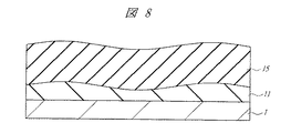
図8および図9は、図6に続く半導体装置の製造工程中における断面図であり、図10は図9の上面図(平面図)である。図10のA−A線の断面図が図9に対応する。図8および図9においても、理解を簡単にするために、半導体基板1の主面に平行な方向の寸法に対して半導体基板1の主面に垂直な方向(厚み方向)の寸法を誇張して描いてある。このため、例えば絶縁膜11およびフォトレジスト膜15の膜厚なども誇張して描いてある。
【0030】
上記のように絶縁膜11の膜厚分布を測定(ステップS3)した後、図8に示されるように、絶縁膜11上に感光性材料からなる膜(感光性材料膜)、ここではフォトレジスト膜15を形成する(ステップS4)。フォトレジスト膜15は、例えばネガ型のフォトレジスト膜である。他の形態として、フォトレジスト膜15にポジ型のフォトレジスト膜を用いることも可能である。ネガ型またはポジ型のフォトレジスト膜を用いることで、膜厚を容易に露光量でコントロールすることが出来る利点がある。また、フォトレジスト膜15の代わりに感光性ポリイミド膜などの他の感光性材料膜を用いることもできる。
【0031】
フォトレジスト膜15を均一な膜厚に形成しても、上記のように下地の絶縁膜11の膜厚分布が不均一で絶縁膜11の上面にうねり(ゆるやかな凹凸)が生じている場合、図8に模式的に示されるように、フォトレジスト膜15の上面にも下地の絶縁膜11を反映したうねり(ゆるやかな凹凸)が生じる。
【0032】
次に、フォトレジスト膜15を露光する(ステップS5)。この際、絶縁膜11の膜厚分布に対応した露光量(露光エネルギー、露光強度)分布でフォトレジスト膜15(半導体基板1)が露光される。本実施の形態では、後述する現像処理後のフォトレジスト膜15の残存膜厚と絶縁膜11の膜厚との和が半導体基板1の面内(主面内)で均一になるような露光量分布で、フォトレジスト膜15を露光処理する。
【0033】
半導体基板1上のフォトレジスト膜15の露光処理は、複数のショットによって行われる。図9および図10に示されるように、例えば、1回のショットによって露光される領域が区画13に対応し、区画13の数に対応するショット数の露光が行われて、全区画13すなわちフォトレジスト膜15全体の露光処理が行われる。
【0034】
図11は、各区画13(の中心位置14)において測定された絶縁膜11の膜厚t1とその区画13(を露光するショット)の露光量(露光エネルギー、露光強度)との関係を示すグラフである。図11のグラフの横軸は、各区画13(の中心位置14)において測定された絶縁膜11の膜厚t1(任意単位:arbitrary unit)に対応し、縦軸は、その区画13を露光するショットの露光量(任意単位:arbitrary unit)に対応する。本実施の形態では、各区画13に対して露光(ショット)を行う際の露光量(露光エネルギー、露光強度)を各ショット毎に調整し、例えば図11に示されるように、絶縁膜11の膜厚t1が相対的に薄かった区画13(例えば区画13a)では露光量を相対的に大きくし、絶縁膜11の膜厚が相対的に厚かった区画13(例えば区画13b)では露光量を相対的に小さくする。予め図11に示されるような絶縁膜11の膜厚t1と露光量との相関関係を理論的または実験的に求めて記憶装置に記憶しておき、図9および図10に示されるように各区画13を露光する際に、コンピュータが各区画13での絶縁膜11の膜厚t1に対応する露光量を記憶装置から読み出して選択し、選択された露光量で各区画13を露光することで、半導体基板1面内の露光量分布を調整することもできる。また、各区画13の露光の際には、レチクル(マスク)は不要であり、一つの区画13内は均等に露光することができる。
【0035】
図12は、図9に続く半導体装置の製造工程中における断面図である。図12においても、理解を簡単にするために、半導体基板1の主面に平行な方向の寸法に対して半導体基板1の主面に垂直な方向(厚み方向)の寸法を誇張して描いてある。このため、例えば絶縁膜11およびフォトレジスト膜15の膜厚なども誇張して描いてある。
【0036】
上記のようにフォトレジスト膜15の露光処理(ステップS5)を行った後、図12に示されるように、フォトレジスト膜15の現像処理を行う(ステップS6)。
【0037】
図13は、ネガ型のフォトレジスト膜15を露光し現像処理した場合のフォトレジスト膜15の残存膜厚t2の露光量(露光エネルギー、露光強度)に対する依存性を模式的に示すグラフである。図13のグラフの横軸は、各区画13を露光するショットの露光量(任意単位:arbitrary unit)に対応し、縦軸は、現像処理後のその区画13におけるフォトレジスト膜15の残存膜厚t2(任意単位:arbitrary unit)に対応する。図13からも分かるように、各区画13において現像処理後に残存するフォトレジスト膜15の膜厚(残存膜厚)t2は、その区画13を露光した際の露光量に対応し、フォトレジスト膜15がネガ型の場合は、露光量が大きかった領域ほどフォトレジスト膜15の残存膜厚t2が厚くなる。
【0038】
このため、図12に示されるように、露光量が大きかった区画13(例えば区画13a)では現像処理後のフォトレジスト膜15の残存膜厚t2が相対的に厚くなり、露光量が小さかった区画13(例えば区画13b)では現像処理後のフォトレジスト膜15の残存膜厚t2が相対的に薄くなる。上記のように絶縁膜11の膜厚t1が薄かった区画13(例えば区画13a)では露光量を相対的に大きくしているのでフォトレジスト膜15の残存膜厚t2が相対的に厚くなり、絶縁膜11の膜厚t1が厚かった区画13(例えば区画13b)では露光量を相対的に小さくしているのでフォトレジスト膜15の残存膜厚t2が相対的に薄くなる。従って、絶縁膜11の膜厚分布と残存するフォトレジスト膜15の膜厚(残存膜厚)分布とが相殺し、現像処理後のフォトレジスト膜15の残存膜厚t2と絶縁膜11の膜厚t1との和が半導体基板1面内で均一になり、残存するフォトレジスト膜15の上面は半導体基板1の面内(主面内)において全体的に(絶縁膜11の上面よりも)平坦になる。
【0039】
図14および図15は、図12に続く半導体装置の製造工程中における断面図である。図14および図15においても、理解を簡単にするために、半導体基板1の主面に平行な方向の寸法に対して半導体基板1の主面に垂直な方向(厚み方向)の寸法を誇張して描いてある。このため、例えば絶縁膜11の膜厚なども誇張して描いてある。
【0040】
上記のようにフォトレジスト膜15の現像処理(ステップS6)を行った後、図14に示されるように、フォトレジスト膜15および絶縁膜11をエッチングする(ステップS7)。この際、フォトレジスト膜15のエッチング速度(エッチングレート)と絶縁膜11のエッチング速度(エッチングレート)とが同じになるようなエッチング条件で、エッチング処理、例えばプラズマエッチングなどのドライエッチングを行う。エッチングガスとして、例えばAr/O2/CF4/CHF3などを用いることができる。
【0041】
このエッチング処理によって、フォトレジスト膜15の全部と、絶縁膜11の一部とが除去される。上記のように、フォトレジスト膜15に対するエッチング速度と絶縁膜11に対するエッチング速度とが同じになるような条件でエッチング処理を行っているので、エッチング(除去)されたフォトレジスト膜15と絶縁膜11との合計の厚みは、半導体基板1の面内において均一になる。このため、図14に示されるエッチング処理後に残存する絶縁膜11の上面は、図12に示されるエッチング処理前のフォトレジスト膜15の上面の形状を反映したものになる。また、上記のように、エッチング処理(ステップS7)前(現像処理後)のフォトレジスト膜15の残存膜厚t2と絶縁膜11の膜厚t1との和は半導体基板1面内でほぼ均一である。従って、エッチング処理(ステップS7)後に残存する絶縁膜11の上面は、半導体基板1の面内(主面内)において全体的に(絶縁膜11のCMP処理後でフォトレジスト膜15の形成前の絶縁膜11の上面よりも)平坦になり、エッチング処理後に残存する絶縁膜11の半導体基板1の面内(主面内)での膜厚分布が(絶縁膜11のCMP処理後でフォトレジスト膜15の形成前の絶縁膜11の膜厚分布よりも)均一になる。
【0042】
上記のようにフォトレジスト膜15および絶縁膜11のエッチング処理を行った(ステップS7)後、図15に示されるように、絶縁膜11をCMP処理する(ステップS8)ことがより好ましい。これにより、各区画13の境界に存在し得る絶縁膜11の微小な段差を除去することができる。このため、絶縁膜11の上面をより平坦化し、半導体基板1の面内(主面内)での絶縁膜11の膜厚分布をより均一化することができる。また、各区画13の境界に存在し得る絶縁膜11の段差が小さく、悪影響が生じない程度である場合は、このCMP処理(ステップS8)を省略することもできる。
【0043】
図16は、図15に続く半導体装置の製造工程中における要部断面図であり、図1〜図3に対応する要部断面図である。
【0044】
上記のようにして(ステップS1〜S8)絶縁膜11の半導体基板1面内での膜厚分布をより均一化する処理を行った後、図16に示されるように、絶縁膜11上に、コンタクトホール形成用の図示しないフォトレジスト膜を形成し、そのフォトレジスト膜を露光し現像してパターン化し、パターン化されたフォトレジスト膜をエッチングマスクとして用いて絶縁膜11を選択的にドライエッチングすることにより、絶縁膜11にコンタクトホール(スルーホール)21を形成する。コンタクトホール21の底部では、半導体基板1の主面の一部、例えばn+型半導体領域8の一部、やゲート電極5の一部などが露出される。本実施の形態では、上記のように半導体基板1の面内での絶縁膜11の膜厚分布をより均一にすることができるので、コンタクトホール21の形成のためのドライエッチング工程において、オーバーエッチング量を小さくしても絶縁膜11にコンタクトホール21を確実に形成することが可能となる。このため、オーバーエッチングによる半導体基板1(例えばn+型半導体領域8またはゲート電極5)のダメージを抑制または防止することができる。また、絶縁膜11にコンタクトホール21を確実に開口できるので、半導体装置の製造歩留りを向上することができる。
【0045】
次に、コンタクトホール21内に、タングステン(W)などからなるプラグ22が形成される。プラグ22は、例えば、コンタクトホール21の内部を含む絶縁膜11上にバリア膜として例えば窒化チタン膜22aを形成した後、タングステン膜をCVD(Chemical Vapor Deposition)法などによって窒化チタン膜22a上にコンタクトホール21を埋めるように形成し、絶縁膜11上の不要なタングステン膜および窒化チタン膜22aをCMP法またはエッチバック法などによって除去することにより形成することができる。
【0046】
次に、プラグ22が埋め込まれた絶縁膜11上に、配線23が形成される。例えば、プラグ22が埋め込まれた絶縁膜11上に、チタン膜23aと、窒化チタン膜23bと、アルミニウム膜(アルミニウム合金膜)23cと、チタン膜23dと、窒化チタン膜23eとを順に形成し、フォトリソグラフィ法などによって所定のパターンに加工して配線23を形成する。配線23は、プラグ22を介してn+型半導体領域8やゲート電極5と電気的に接続されている。配線23は、上記のようなアルミニウム配線に限定されず種々変更可能であり、例えばアルミニウム(Al)またはアルミニウム合金などの単体膜からなるアルミニウム配線や、タングステン配線、あるいは銅配線(ダマシン法を用いた埋込銅配線)とすることもできる。
【0047】
次に、絶縁膜11上に、配線23を覆うように、例えば酸化シリコン膜などからなる絶縁膜(層間絶縁膜)24が形成される。それから、絶縁膜24がCMP処理されて、絶縁膜24の上面が平坦化される。そして、上記絶縁膜11と同様の手法(ステップS3〜S8)を用いて絶縁膜24の上面をより平坦化し、半導体基板1面内での絶縁膜24の膜厚分布をより均一化する。すなわち、半導体基板1面内での絶縁膜24の膜厚分布を測定し、絶縁膜24上にフォトレジスト膜を形成し、そのフォトレジスト膜を絶縁膜24の膜厚分布に対応した露光量分布で露光し、現像した後、フォトレジスト膜の全部と絶縁膜24の一部とをエッチングし、必要に応じて絶縁膜24をCMP処理する。その後、絶縁膜24にスルーホールおよびそこに埋め込まれるプラグが上記コンタクトホール21およびプラグ22と同様にして形成され、更にプラグが埋め込まれた絶縁膜24上に配線23と同様にして上層配線が形成されるが、ここではその説明は省略する。
【0048】
本実施の形態では、半導体基板1上に絶縁膜11を形成し、半導体基板1面内での絶縁膜11の膜厚分布を測定し、絶縁膜11上にフォトレジスト膜(感光性材料膜)15を形成し、絶縁膜11の膜厚分布に対応した露光量分布でフォトレジスト膜15の露光処理を行う。これにより、現像処理後に残存するフォトレジスト膜15の半導体基板1面内での膜厚分布が、絶縁膜11の半導体基板1面内での膜厚分布と相殺され、絶縁膜11とフォトレジスト膜15の合計の膜厚(すなわち絶縁膜11の膜厚t1とフォトレジスト膜15の残存膜厚t2との和)が半導体基板1面内で均一になる。その後、フォトレジスト膜15の全部と絶縁膜11の一部(上層部分)とをドライエッチングによって除去する。このようにして、半導体基板1上に形成された絶縁膜11の半導体基板1面内での膜厚分布を(フォトレジスト膜15の形成前の絶縁膜11の膜厚分布よりも)均一にすることができる。
【0049】
半導体基板1面内での絶縁膜の膜厚分布が不均一であると、その膜厚分布が不均一な絶縁膜にコンタクトホール(スルーホール)などをドライエッチング法で形成する際に、絶縁膜が相対的に厚い領域ではコンタクトホール(スルーホール)が非開口となる恐れがある。これを防止し、半導体基板1面内のいずれの領域においてもコンタクトホール(スルーホール)を確実に開口するには、ドライエッチング工程におけるオーバーエッチング量を比較的大きくする必要があるが、オーバーエッチングによるエッチングストッパ膜の突き抜けや半導体基板1(例えばn+型半導体領域8またはゲート電極5)へダメージを与える恐れがある。これらは、半導体装置の製造歩留りを低下させる。本実施の形態では、半導体基板1上に形成した絶縁膜11の半導体基板1面内での膜厚分布を均一にすることができるので、絶縁膜11にコンタクトホール(スルーホール)を形成した際の開口不良を防止できる。また、絶縁膜11にコンタクトホール(スルーホール)を形成するためのドライエッチング工程におけるオーバーエッチング量を比較的小さくすることができるので、オーバーエッチングによるエッチングストッパ膜の突き抜けや半導体基板1へのダメージを防止することができる。このため、半導体装置の製造歩留りを向上できる。
【0050】
また、半導体基板上に形成した材料膜(絶縁膜11)の半導体基板面内でも膜厚を均一にできるので、エッチングなどのプロセスマージン(加工マージン)を拡大し、プロセスの選択肢が広がり、工程簡略化や安価なプロセスを選択することができるようになる。このため、半導体装置の製造工程におけるプロセスマージンを拡大し、安定した加工が行え、半導体装置の製造歩留りを向上できる。また、プロセスの簡略化などにより、半導体装置の製造コストを低減できる。
【0051】
また、本実施の形態は、大口径の(すなわち直径が比較的大きな)半導体基板、例えば直径が300mm以上の半導体基板を用いる場合に適用すれば、より好適である。半導体基板の直径が大きいと、半導体基板上に形成された材料膜に対してCMP処理を施しても、その材料膜の上面にはうねり(ゆるやかな凹凸)が生じ、半導体基板1面内での膜厚分布が不均一になりやすい。本実施の形態では、上記(ステップS3〜S8)のようにして半導体基板上に形成された材料膜(絶縁膜11)の半導体基板面内での膜厚分布を均一化する処理を行うことで、半導体基板面内での膜厚分布が不均一になりやすい大口径の半導体基板、例えば直径300mm以上の半導体ウエハにおいても、半導体基板上に均一な材料膜を形成することができ、半導体装置の製造歩留まりを著しく向上することが可能となる。
【0052】
また、本実施の形態は、多層配線構造を形成する半導体装置の製造工程に適用することもできる。この場合、上層の層間絶縁膜ほど成膜段階に生じる段差がきつくなるが、各層間絶縁膜、特に上層の層間絶縁膜を本実施の形態の絶縁膜11と同様にして平坦化処理することで、信頼性に優れた多層配線構造を形成することが可能となる。
【0053】
以上、本発明者によってなされた発明をその実施の形態に基づき具体的に説明したが、本発明は前記実施の形態に限定されるものではなく、その要旨を逸脱しない範囲で種々変更可能であることは言うまでもない。
【0054】
前記実施の形態では、nチャネル型のMISFETを形成する場合について説明したが、種々の半導体装置の製造工程に適用することができる。
【0055】
【発明の効果】
本願において開示される発明のうち、代表的なものによって得られる効果を簡単に説明すれば以下のとおりである。
【0056】
半導体基板上に形成した第1材料膜の膜厚分布を測定し、測定した第1材料膜の膜厚分布に対応して選択した露光量分布で第1材料膜上に形成した第2感光性材料膜を露光処理し、現像処理後に残存する第2感光性材料膜と第1材料膜とをエッチングすることにより、半導体装置の製造歩留りを向上できる。
【図面の簡単な説明】
【図1】本発明の一実施の形態である半導体装置の製造工程中の要部断面図である。
【図2】図1に続く半導体装置の製造工程中における要部断面図である。
【図3】図2に続く半導体装置の製造工程中における要部断面図である。
【図4】半導体基板上に形成した絶縁膜をCMP処理して絶縁膜の上面を平坦化した状態を模式的に示す断面図である。
【図5】半導体基板上に形成した絶縁膜の半導体基板面内の膜厚均一性を向上する処理を説明するためのフローチャートである。
【図6】図4に続く半導体装置の製造工程中における断面図である。
【図7】図6の上面図である。
【図8】図6に続く半導体装置の製造工程中における断面図である。
【図9】図8に続く半導体装置の製造工程中における断面図である。
【図10】図9の上面図である。
【図11】各区画において測定された絶縁膜の膜厚とその区画の露光量との関係を示すグラフである。
【図12】図9に続く半導体装置の製造工程中における断面図である。
【図13】ネガ型のフォトレジスト膜を露光し現像処理した場合のフォトレジスト膜の残存膜厚の露光量に対する依存性を模式的に示すグラフである。
【図14】図12に続く半導体装置の製造工程中における断面図である。
【図15】図14に続く半導体装置の製造工程中における断面図である。
【図16】図15に続く半導体装置の製造工程中における要部断面図である。
【符号の説明】
1 半導体基板
2 素子分離領域
3 p型ウエル
4 ゲート絶縁膜
5 ゲート電極
6 n−型半導体領域
7 サイドウォールスペーサ
8 n+型半導体領域
9 nチャネル型のMISFET
11 絶縁膜
12a 凹部
12b 凸部
13 区画
13a 区画
13b 区画
14 中心位置
15 フォトレジスト膜
21 コンタクトホール
22 プラグ
22a 窒化チタン膜
23 配線
23a チタン膜
23b 窒化チタン膜
23c アルミニウム膜
23d チタン膜
23e 窒化チタン膜
24 絶縁膜[0001]
BACKGROUND OF THE INVENTION
The present invention relates to a manufacturing technique of a semiconductor device, and more particularly to a technique effective when applied to uniform film thickness of an interlayer insulating film within a semiconductor substrate surface.
[0002]
[Prior art]
After forming a semiconductor element such as MISFET on the semiconductor substrate, an interlayer insulating film is formed on the semiconductor substrate. The formed interlayer insulating film is subjected to CMP to planarize the upper surface.
[0003]
In Japanese Patent Laid-Open No. 2002-299256, a plurality of holes for introducing reactive gases are provided to face the surface of the substrate to be processed in order to eliminate the non-uniformity of the film thickness distribution of the film formation on the substrate to be processed. In the semiconductor manufacturing apparatus having the shower head arranged as described above, the gas flow rate A is blown out from the first hole on the first circumference closest to the center of the substrate to be processed, and the outside of the first circumference. By the position of the second hole on the second circumference of the gas, the gas reacts and the flow rate of the gas changes from the flow rate A to the flow rate A-flow rate B, and the flow rate of the gas changed to the flow rate A-flow rate B In order to return to the flow rate A, the flow rate B is added at the position of the second hole on the second circumference, and the flow rate is returned to A on each circumference having the holes in this way, so Describes a technique in which the flow rate of gas in the cylinder is not substantially changed (see Patent Document 1).
[0004]
[Patent Document 1]
JP 2002-299256 A
[0005]
[Problems to be solved by the invention]
According to the study of the present inventor, the following has been found.
[0006]
When a material film such as an interlayer insulating film is formed on a semiconductor substrate and CMP processing is performed, the upper surface of the interlayer insulating film (material film) is locally flattened. Waviness (gradual unevenness) occurs on the upper surface of the interlayer insulating film, and the film thickness distribution of the interlayer insulating film in the semiconductor substrate surface becomes non-uniform. Such a phenomenon tends to become more prominent as the diameter of the semiconductor substrate increases. If the thickness distribution of the interlayer insulating film in the semiconductor substrate surface is non-uniform, when a through hole or the like is formed in the interlayer insulating film by a dry etching method, the through hole is not formed in a region where the interlayer insulating film is relatively thick. There is a risk of non-opening. In order to prevent this and to reliably open the through hole in any region in the semiconductor substrate surface, it is necessary to make the overetching amount relatively large in the dry etching process, but the etching stopper film penetrates by overetching. Or damage to the semiconductor substrate. These lower the manufacturing yield of the semiconductor device. For this reason, it is preferable to make the film thickness distribution of the interlayer insulating film (material film) in the semiconductor substrate surface more uniform.
[0007]
[0008]
An object of the present invention is to provide a method of manufacturing a semiconductor device that can improve the manufacturing yield of the semiconductor device.
[0009]
Another object of the present invention is to provide a method of manufacturing a semiconductor device that can improve the uniformity of the film thickness distribution in the semiconductor substrate surface of the material film formed on the semiconductor substrate.
[0010]
The above and other objects and novel features of the present invention will be apparent from the description of this specification and the accompanying drawings.
[0011]
[Means for Solving the Problems]
Of the inventions disclosed in the present application, the outline of typical ones will be briefly described as follows.
[0012]
The method for manufacturing a semiconductor device of the present invention measures the film thickness distribution of the first material film formed on the semiconductor substrate, and the first exposure dose distribution is selected corresponding to the measured film thickness distribution of the first material film. The second photosensitive material film formed on the material film is subjected to an exposure process, and the second photosensitive material film and the first material film remaining after the development process are etched.
[0013]
DETAILED DESCRIPTION OF THE INVENTION
Hereinafter, embodiments of the present invention will be described in detail with reference to the drawings. Note that components having the same function are denoted by the same reference symbols throughout the drawings for describing the embodiments, and the repetitive description thereof will be omitted. In the following embodiments, the description of the same or similar parts will not be repeated in principle unless particularly necessary.
[0014]
(Embodiment 1)
A manufacturing process of the semiconductor device of the present embodiment will be described with reference to the drawings. 1 to 3 are fragmentary cross-sectional views of a semiconductor device according to an embodiment of the present invention, such as a MISFET (Metal Insulator Semiconductor Field Effect Transistor), during a manufacturing process.
[0015]
As shown in FIG. 1, for example, a semiconductor substrate (semiconductor wafer) 1 made of p-type single crystal silicon having a specific resistance of about 1 to 10 Ωcm is prepared (prepared), and element isolation is performed on the main surface of the
[0016]
Next, the p-type well 3 is formed by ion-implanting impurities such as boron (B) into the region of the
[0017]
Next, a
[0018]
Next, a
[0019]
Next, an impurity such as phosphorus (P) is ion-implanted into regions on both sides of the
[0020]
Next, side walls or side wall spacers (side wall spacers) 7 made of, for example, silicon oxide are formed on the side walls of the
[0021]
After the formation of the
[0022]
In this way, a structure as shown in FIG. 1 is obtained, and an n-channel MISFET (Metal Insulator Semiconductor Field Effect Transistor) 9 is formed in the p-type well 3.
[0023]
Although not shown, the
[0024]
Next, as shown in FIG. 2, an insulating film (interlayer insulating film) 11 is formed on the entire main surface (main surface on the
[0025]
In FIG. 4, an insulating
[0026]
Even if the insulating
[0027]
FIG. 5 is a flowchart for explaining a process of improving the film thickness uniformity in the surface of the
[0028]
As described above, the insulating
[0029]
8 and 9 are cross-sectional views in the manufacturing process of the semiconductor device subsequent to FIG. 6, and FIG. 10 is a top view (plan view) of FIG. A sectional view taken along line AA in FIG. 10 corresponds to FIG. 8 and 9 also exaggerate the dimension in the direction (thickness direction) perpendicular to the main surface of the
[0030]
After measuring the film thickness distribution of the insulating
[0031]
Even when the
[0032]
Next, the
[0033]
The exposure process of the
[0034]
FIG. 11 shows the film thickness t of the insulating
[0035]
FIG. 12 is a cross-sectional view of the semiconductor device during a manufacturing step following that of FIG. Also in FIG. 12, for the sake of easy understanding, the dimension in the direction perpendicular to the main surface of the semiconductor substrate 1 (thickness direction) is exaggerated with respect to the dimension in the direction parallel to the main surface of the
[0036]
After the exposure process (step S5) of the
[0037]
FIG. 13 shows the remaining film thickness t of the
[0038]
For this reason, as shown in FIG. 12, the remaining film thickness t of the
[0039]
14 and 15 are cross-sectional views of the semiconductor device during the manufacturing process subsequent to FIG. 14 and 15 also exaggerate the dimension in the direction perpendicular to the main surface of the semiconductor substrate 1 (thickness direction) with respect to the dimension in the direction parallel to the main surface of the
[0040]
After performing the development process (step S6) of the
[0041]
By this etching process, the
[0042]
More preferably, after the
[0043]
16 is a fragmentary cross-sectional view of the semiconductor device during a manufacturing step following that of FIG. 15, and is a fragmentary cross-sectional view corresponding to FIGS. 1 to 3.
[0044]
As described above (steps S1 to S8), after performing the process of making the film thickness distribution of the insulating
[0045]
Next, a
[0046]
Next, the
[0047]
Next, an insulating film (interlayer insulating film) 24 made of, for example, a silicon oxide film is formed on the insulating
[0048]
In the present embodiment, an insulating
[0049]
If the film thickness distribution of the insulating film in the surface of the
[0050]
In addition, since the film thickness of the material film (insulating film 11) formed on the semiconductor substrate can be made uniform even within the semiconductor substrate surface, the process margin (processing margin) such as etching is expanded, process options are expanded, and the process is simplified. And cheaper processes can be selected. For this reason, the process margin in the manufacturing process of the semiconductor device can be expanded, stable processing can be performed, and the manufacturing yield of the semiconductor device can be improved. Further, the manufacturing cost of the semiconductor device can be reduced by simplifying the process.
[0051]
Further, this embodiment is more suitable when applied to a semiconductor substrate having a large diameter (that is, a relatively large diameter), for example, a semiconductor substrate having a diameter of 300 mm or more. If the diameter of the semiconductor substrate is large, even if the CMP process is performed on the material film formed on the semiconductor substrate, the upper surface of the material film is wavy (loose unevenness), and the surface of the
[0052]
The present embodiment can also be applied to a manufacturing process of a semiconductor device that forms a multilayer wiring structure. In this case, the step formed in the film formation stage becomes more severe as the upper interlayer insulating film is formed. By flattening each interlayer insulating film, in particular, the upper interlayer insulating film in the same manner as the insulating
[0053]
Although the invention made by the present inventor has been specifically described based on the embodiment, the invention is not limited to the embodiment and can be variously modified without departing from the scope of the invention. Needless to say.
[0054]
Although the case where an n-channel MISFET is formed has been described in the above embodiment, the present invention can be applied to various semiconductor device manufacturing processes.
[0055]
【The invention's effect】
Among the inventions disclosed in the present application, effects obtained by typical ones will be briefly described as follows.
[0056]
The film thickness distribution of the first material film formed on the semiconductor substrate is measured, and the second photosensitivity formed on the first material film with the exposure amount distribution selected corresponding to the measured film thickness distribution of the first material film. The manufacturing yield of the semiconductor device can be improved by exposing the material film and etching the second photosensitive material film and the first material film remaining after the developing process.
[Brief description of the drawings]
FIG. 1 is a fragmentary sectional view in a manufacturing process of a semiconductor device in an embodiment of the invention;
FIG. 2 is a fragmentary cross-sectional view of the semiconductor device during a manufacturing step following that of FIG. 1;
3 is a fragmentary cross-sectional view of the semiconductor device during a manufacturing step following that of FIG. 2; FIG.
FIG. 4 is a cross-sectional view schematically showing a state in which an insulating film formed on a semiconductor substrate is subjected to a CMP process to flatten the upper surface of the insulating film.
FIG. 5 is a flowchart for explaining processing for improving film thickness uniformity in a semiconductor substrate surface of an insulating film formed on a semiconductor substrate.
6 is a cross-sectional view of the semiconductor device during a manufacturing step following that of FIG. 4; FIG.
7 is a top view of FIG. 6. FIG.
8 is a cross-sectional view of the semiconductor device during a manufacturing step following that of FIG. 6; FIG.
FIG. 9 is a cross-sectional view of the semiconductor device during a manufacturing step following that of FIG. 8;
10 is a top view of FIG. 9. FIG.
FIG. 11 is a graph showing the relationship between the thickness of the insulating film measured in each section and the exposure amount in that section.
12 is a cross-sectional view of the semiconductor device during a manufacturing step following that of FIG. 9; FIG.
FIG. 13 is a graph schematically showing the dependency of the remaining film thickness of the photoresist film on the exposure amount when the negative photoresist film is exposed and developed.
14 is a cross-sectional view of the semiconductor device during a manufacturing step following that of FIG. 12; FIG.
15 is a cross-sectional view of the semiconductor device during a manufacturing step following that of FIG. 14; FIG.
16 is a fragmentary cross-sectional view of the semiconductor device during a manufacturing step following that of FIG. 15; FIG.
[Explanation of symbols]
1 Semiconductor substrate
2 Device isolation region
3 p-type well
4 Gate insulation film
5 Gate electrode
6 n − Type semiconductor region
7 Sidewall spacer
8 n + Type semiconductor region
9 n-channel MISFET
11 Insulating film
12a recess
12b Convex part
13 sections
13a section
13b section
14 Center position
15 Photoresist film
21 Contact hole
22 plug
22a Titanium nitride film
23 Wiring
23a Titanium film
23b Titanium nitride film
23c Aluminum film
23d titanium film
23e Titanium nitride film
24 Insulating film
Claims (5)
(a)半導体基板を準備する工程、
(b)前記半導体基板上に第1材料膜を形成する工程、
(c)前記半導体基板の主面内における前記第1材料膜の膜厚分布を測定する工程、
(d)前記第1材料膜上に、感光性材料からなる第2材料膜を形成する工程、
(e)前記(c)工程で測定した前記第1材料膜の膜厚分布に対応した露光量分布で前記第2材料膜を露光処理する工程、
(f)前記第2材料膜を現像処理する工程、
(g)前記第2材料膜および前記第1材料膜をエッチングする工程。A method of manufacturing a semiconductor device comprising the following steps:
(A) a step of preparing a semiconductor substrate;
(B) forming a first material film on the semiconductor substrate;
(C) measuring the thickness distribution of the first material film in the main surface of the semiconductor substrate;
(D) forming a second material film made of a photosensitive material on the first material film;
(E) a step of exposing the second material film with an exposure amount distribution corresponding to the film thickness distribution of the first material film measured in the step (c);
(F) a step of developing the second material film;
(G) A step of etching the second material film and the first material film.
前記(f)工程における前記現像処理後の前記第2材料膜の残存膜厚と前記第1材料膜の膜厚との和が前記半導体基板の主面内で均一になるような露光量分布で、前記(e)工程における前記第2材料膜の露光処理を行うことを特徴とする半導体装置の製造方法。In the manufacturing method of the semiconductor device according to claim 1,
The exposure distribution is such that the sum of the remaining thickness of the second material film after the development process and the thickness of the first material film in the step (f) is uniform in the main surface of the semiconductor substrate. A method for manufacturing a semiconductor device, comprising performing an exposure process on the second material film in the step (e).
前記(g)工程では、前記第2材料膜のエッチング速度と前記第1材料膜のエッチング速度とが同じになるようなエッチング条件でエッチングを行い、前記第2材料膜の全部と前記第1材料膜の一部とを除去することを特徴とする半導体装置の製造方法。In the manufacturing method of the semiconductor device according to claim 1,
In the step (g), etching is performed under an etching condition such that the etching rate of the second material film and the etching rate of the first material film are the same, and the entire second material film and the first material are formed. A method for manufacturing a semiconductor device, wherein a part of the film is removed.
前記(g)工程の後に、前記第1材料膜を化学的機械的研磨する工程を更に有することを特徴とする半導体装置の製造方法。In the manufacturing method of the semiconductor device according to claim 1,
The method of manufacturing a semiconductor device, further comprising a step of chemically mechanically polishing the first material film after the step (g).
前記第2材料膜は、フォトレジスト膜であることを特徴とする半導体装置の製造方法。In the manufacturing method of the semiconductor device according to claim 1,
The method of manufacturing a semiconductor device, wherein the second material film is a photoresist film.
Priority Applications (1)
| Application Number | Priority Date | Filing Date | Title |
|---|---|---|---|
| JP2003193297A JP2005032785A (en) | 2003-07-08 | 2003-07-08 | Method of manufacturing semiconductor device |
Applications Claiming Priority (1)
| Application Number | Priority Date | Filing Date | Title |
|---|---|---|---|
| JP2003193297A JP2005032785A (en) | 2003-07-08 | 2003-07-08 | Method of manufacturing semiconductor device |
Publications (1)
| Publication Number | Publication Date |
|---|---|
| JP2005032785A true JP2005032785A (en) | 2005-02-03 |
Family
ID=34204803
Family Applications (1)
| Application Number | Title | Priority Date | Filing Date |
|---|---|---|---|
| JP2003193297A Pending JP2005032785A (en) | 2003-07-08 | 2003-07-08 | Method of manufacturing semiconductor device |
Country Status (1)
| Country | Link |
|---|---|
| JP (1) | JP2005032785A (en) |
Cited By (2)
| Publication number | Priority date | Publication date | Assignee | Title |
|---|---|---|---|---|
| JP2009021603A (en) * | 2007-07-12 | 2009-01-29 | Samsung Electronics Co Ltd | Semiconductor device and manufacturing method thereof |
| JP2016225495A (en) * | 2015-06-01 | 2016-12-28 | 株式会社日立国際電気 | Method for manufacturing semiconductor device, substrate processing system, substrate processing device, and program |
-
2003
- 2003-07-08 JP JP2003193297A patent/JP2005032785A/en active Pending
Cited By (2)
| Publication number | Priority date | Publication date | Assignee | Title |
|---|---|---|---|---|
| JP2009021603A (en) * | 2007-07-12 | 2009-01-29 | Samsung Electronics Co Ltd | Semiconductor device and manufacturing method thereof |
| JP2016225495A (en) * | 2015-06-01 | 2016-12-28 | 株式会社日立国際電気 | Method for manufacturing semiconductor device, substrate processing system, substrate processing device, and program |
Similar Documents
| Publication | Publication Date | Title |
|---|---|---|
| JP4398467B2 (en) | Manufacturing method of semiconductor device | |
| US6838388B2 (en) | Fabrication method of semiconductor integrated circuit device | |
| US7504287B2 (en) | Methods for fabricating an integrated circuit | |
| TWI251296B (en) | Method for fabricating semiconductor device capable of preventing damage by wet cleaning process | |
| EP0895283A2 (en) | Method of forming multi-level coplanar metal/insulator films using dual damascene with sacreficial flowable oxide | |
| TW201349510A (en) | Integrated circuit, semiconductor structure and manufacturing method thereof | |
| CN109427651B (en) | Semiconductor structure and forming method thereof | |
| TWI626677B (en) | Manufacturing method of integrated circuit and semiconductor component | |
| JP4711658B2 (en) | Manufacturing method of semiconductor device having fine pattern | |
| CN110718462B (en) | Method for fabricating semiconductor structure on semiconductor wafer | |
| US20080261397A1 (en) | Method for Manufacturing Semiconductor Device | |
| US20080150142A1 (en) | Multilevel wiring, laminated aluminum wiring, semiconductor device and manufacturing method of the same | |
| JP3436263B2 (en) | Method for forming conformal H-rich Si3N4 layer | |
| JP2003243293A (en) | Manufacturing method for semiconductor device | |
| JP2005032785A (en) | Method of manufacturing semiconductor device | |
| US20070013070A1 (en) | Semiconductor devices and methods of manufacture thereof | |
| JP2007027348A (en) | Semiconductor device and its manufacturing method | |
| JP2004356386A (en) | Semiconductor device and its manufacturing method | |
| US20050277254A1 (en) | Methods of forming device with recessed gate electrodes | |
| US7592268B2 (en) | Method for fabricating semiconductor device | |
| KR100790816B1 (en) | Wiring Manufacturing Method of Semiconductor Memory Device | |
| KR100811449B1 (en) | Semiconductor device and manufacturing method thereof | |
| JPH11204751A (en) | Method for manufacturing semiconductor device | |
| JPH06177236A (en) | Manufacture of element isolation film of trench structure | |
| US20060278607A1 (en) | Method for fabricating semiconductor device with step gated asymmetric recess structure |
Legal Events
| Date | Code | Title | Description |
|---|---|---|---|
| A711 | Notification of change in applicant |
Free format text: JAPANESE INTERMEDIATE CODE: A712 Effective date: 20050318 |