JP2005019759A - Semiconductor wafer surface protecting adhesive film and semiconductor wafer protecting method using the adhesive film - Google Patents
Semiconductor wafer surface protecting adhesive film and semiconductor wafer protecting method using the adhesive film Download PDFInfo
- Publication number
- JP2005019759A JP2005019759A JP2003183637A JP2003183637A JP2005019759A JP 2005019759 A JP2005019759 A JP 2005019759A JP 2003183637 A JP2003183637 A JP 2003183637A JP 2003183637 A JP2003183637 A JP 2003183637A JP 2005019759 A JP2005019759 A JP 2005019759A
- Authority
- JP
- Japan
- Prior art keywords
- semiconductor wafer
- adhesive film
- protecting
- film
- adhesive
- Prior art date
- Legal status (The legal status is an assumption and is not a legal conclusion. Google has not performed a legal analysis and makes no representation as to the accuracy of the status listed.)
- Pending
Links
- 239000004065 semiconductor Substances 0.000 title claims abstract description 191
- 239000002313 adhesive film Substances 0.000 title claims abstract description 132
- 238000000034 method Methods 0.000 title claims abstract description 85
- 239000010410 layer Substances 0.000 claims abstract description 58
- 229920005989 resin Polymers 0.000 claims abstract description 31
- 239000011347 resin Substances 0.000 claims abstract description 31
- 230000001681 protective effect Effects 0.000 claims abstract description 24
- 230000008859 change Effects 0.000 claims abstract description 14
- 238000002844 melting Methods 0.000 claims abstract description 9
- 230000008018 melting Effects 0.000 claims abstract description 9
- 238000004519 manufacturing process Methods 0.000 claims description 26
- 238000003860 storage Methods 0.000 claims description 21
- 239000012790 adhesive layer Substances 0.000 claims description 20
- 238000012545 processing Methods 0.000 claims description 16
- 229920000106 Liquid crystal polymer Polymers 0.000 claims description 6
- 239000004977 Liquid-crystal polymers (LCPs) Substances 0.000 claims description 6
- 239000005038 ethylene vinyl acetate Substances 0.000 claims description 4
- 229920001200 poly(ethylene-vinyl acetate) Polymers 0.000 claims description 4
- 239000004820 Pressure-sensitive adhesive Substances 0.000 abstract description 70
- 230000008569 process Effects 0.000 abstract description 30
- 235000012431 wafers Nutrition 0.000 description 210
- 230000001070 adhesive effect Effects 0.000 description 43
- 239000000853 adhesive Substances 0.000 description 42
- 239000000178 monomer Substances 0.000 description 33
- -1 aromatic diol Chemical class 0.000 description 24
- 238000000227 grinding Methods 0.000 description 21
- 238000000576 coating method Methods 0.000 description 19
- 239000011248 coating agent Substances 0.000 description 18
- NIXOWILDQLNWCW-UHFFFAOYSA-N acrylic acid group Chemical group C(C=C)(=O)O NIXOWILDQLNWCW-UHFFFAOYSA-N 0.000 description 17
- 239000003431 cross linking reagent Substances 0.000 description 15
- 125000000524 functional group Chemical group 0.000 description 13
- RTZKZFJDLAIYFH-UHFFFAOYSA-N Diethyl ether Chemical compound CCOCC RTZKZFJDLAIYFH-UHFFFAOYSA-N 0.000 description 12
- 238000010438 heat treatment Methods 0.000 description 11
- 239000003795 chemical substances by application Substances 0.000 description 9
- 239000000203 mixture Substances 0.000 description 9
- 238000004140 cleaning Methods 0.000 description 8
- 230000000052 comparative effect Effects 0.000 description 8
- 238000011109 contamination Methods 0.000 description 8
- 239000000839 emulsion Substances 0.000 description 8
- 238000005259 measurement Methods 0.000 description 8
- XUIMIQQOPSSXEZ-UHFFFAOYSA-N Silicon Chemical compound [Si] XUIMIQQOPSSXEZ-UHFFFAOYSA-N 0.000 description 7
- 229910052710 silicon Inorganic materials 0.000 description 7
- 239000010703 silicon Substances 0.000 description 7
- 239000004094 surface-active agent Substances 0.000 description 7
- VFXXTYGQYWRHJP-UHFFFAOYSA-N 4,4'-azobis(4-cyanopentanoic acid) Chemical compound OC(=O)CCC(C)(C#N)N=NC(C)(CCC(O)=O)C#N VFXXTYGQYWRHJP-UHFFFAOYSA-N 0.000 description 6
- 239000007788 liquid Substances 0.000 description 6
- 229910052757 nitrogen Inorganic materials 0.000 description 6
- 238000012546 transfer Methods 0.000 description 6
- XLYOFNOQVPJJNP-UHFFFAOYSA-N water Substances O XLYOFNOQVPJJNP-UHFFFAOYSA-N 0.000 description 6
- 238000004132 cross linking Methods 0.000 description 5
- 238000005520 cutting process Methods 0.000 description 5
- 238000007720 emulsion polymerization reaction Methods 0.000 description 5
- 125000001997 phenyl group Chemical group [H]C1=C([H])C([H])=C(*)C([H])=C1[H] 0.000 description 5
- 238000006116 polymerization reaction Methods 0.000 description 5
- 125000006017 1-propenyl group Chemical group 0.000 description 4
- HRPVXLWXLXDGHG-UHFFFAOYSA-N Acrylamide Chemical compound NC(=O)C=C HRPVXLWXLXDGHG-UHFFFAOYSA-N 0.000 description 4
- VZCYOOQTPOCHFL-OWOJBTEDSA-N Fumaric acid Chemical compound OC(=O)\C=C\C(O)=O VZCYOOQTPOCHFL-OWOJBTEDSA-N 0.000 description 4
- WOBHKFSMXKNTIM-UHFFFAOYSA-N Hydroxyethyl methacrylate Chemical compound CC(=C)C(=O)OCCO WOBHKFSMXKNTIM-UHFFFAOYSA-N 0.000 description 4
- CERQOIWHTDAKMF-UHFFFAOYSA-N Methacrylic acid Chemical compound CC(=C)C(O)=O CERQOIWHTDAKMF-UHFFFAOYSA-N 0.000 description 4
- MTHSVFCYNBDYFN-UHFFFAOYSA-N anhydrous diethylene glycol Natural products OCCOCCO MTHSVFCYNBDYFN-UHFFFAOYSA-N 0.000 description 4
- 230000001588 bifunctional effect Effects 0.000 description 4
- 238000001035 drying Methods 0.000 description 4
- 150000002148 esters Chemical class 0.000 description 4
- 150000002978 peroxides Chemical class 0.000 description 4
- 229920000642 polymer Polymers 0.000 description 4
- VZCYOOQTPOCHFL-UHFFFAOYSA-N trans-butenedioic acid Natural products OC(=O)C=CC(O)=O VZCYOOQTPOCHFL-UHFFFAOYSA-N 0.000 description 4
- 238000001039 wet etching Methods 0.000 description 4
- GOXQRTZXKQZDDN-UHFFFAOYSA-N 2-Ethylhexyl acrylate Chemical compound CCCCC(CC)COC(=O)C=C GOXQRTZXKQZDDN-UHFFFAOYSA-N 0.000 description 3
- VHUUQVKOLVNVRT-UHFFFAOYSA-N Ammonium hydroxide Chemical compound [NH4+].[OH-] VHUUQVKOLVNVRT-UHFFFAOYSA-N 0.000 description 3
- PEDCQBHIVMGVHV-UHFFFAOYSA-N Glycerine Chemical compound OCC(O)CO PEDCQBHIVMGVHV-UHFFFAOYSA-N 0.000 description 3
- OFOBLEOULBTSOW-UHFFFAOYSA-N Malonic acid Chemical compound OC(=O)CC(O)=O OFOBLEOULBTSOW-UHFFFAOYSA-N 0.000 description 3
- VVQNEPGJFQJSBK-UHFFFAOYSA-N Methyl methacrylate Chemical compound COC(=O)C(C)=C VVQNEPGJFQJSBK-UHFFFAOYSA-N 0.000 description 3
- 239000004743 Polypropylene Substances 0.000 description 3
- DNIAPMSPPWPWGF-UHFFFAOYSA-N Propylene glycol Chemical compound CC(O)CO DNIAPMSPPWPWGF-UHFFFAOYSA-N 0.000 description 3
- 239000002253 acid Substances 0.000 description 3
- 229940114077 acrylic acid Drugs 0.000 description 3
- 125000000217 alkyl group Chemical group 0.000 description 3
- QGZKDVFQNNGYKY-UHFFFAOYSA-N ammonia Natural products N QGZKDVFQNNGYKY-UHFFFAOYSA-N 0.000 description 3
- ROOXNKNUYICQNP-UHFFFAOYSA-N ammonium peroxydisulfate Substances [NH4+].[NH4+].[O-]S(=O)(=O)OOS([O-])(=O)=O ROOXNKNUYICQNP-UHFFFAOYSA-N 0.000 description 3
- VAZSKTXWXKYQJF-UHFFFAOYSA-N ammonium persulfate Chemical compound [NH4+].[NH4+].[O-]S(=O)OOS([O-])=O VAZSKTXWXKYQJF-UHFFFAOYSA-N 0.000 description 3
- 229910001870 ammonium persulfate Inorganic materials 0.000 description 3
- 125000004432 carbon atom Chemical group C* 0.000 description 3
- 125000003178 carboxy group Chemical group [H]OC(*)=O 0.000 description 3
- 238000006243 chemical reaction Methods 0.000 description 3
- 238000003851 corona treatment Methods 0.000 description 3
- 239000002245 particle Substances 0.000 description 3
- 238000005498 polishing Methods 0.000 description 3
- 229920001721 polyimide Polymers 0.000 description 3
- 229920001155 polypropylene Polymers 0.000 description 3
- 238000010526 radical polymerization reaction Methods 0.000 description 3
- 239000002994 raw material Substances 0.000 description 3
- 239000002904 solvent Substances 0.000 description 3
- 239000000126 substance Substances 0.000 description 3
- 239000000758 substrate Substances 0.000 description 3
- 238000005406 washing Methods 0.000 description 3
- MYRTYDVEIRVNKP-UHFFFAOYSA-N 1,2-Divinylbenzene Chemical compound C=CC1=CC=CC=C1C=C MYRTYDVEIRVNKP-UHFFFAOYSA-N 0.000 description 2
- LCPVQAHEFVXVKT-UHFFFAOYSA-N 2-(2,4-difluorophenoxy)pyridin-3-amine Chemical compound NC1=CC=CN=C1OC1=CC=C(F)C=C1F LCPVQAHEFVXVKT-UHFFFAOYSA-N 0.000 description 2
- OZAIFHULBGXAKX-UHFFFAOYSA-N 2-(2-cyanopropan-2-yldiazenyl)-2-methylpropanenitrile Chemical compound N#CC(C)(C)N=NC(C)(C)C#N OZAIFHULBGXAKX-UHFFFAOYSA-N 0.000 description 2
- SMZOUWXMTYCWNB-UHFFFAOYSA-N 2-(2-methoxy-5-methylphenyl)ethanamine Chemical compound COC1=CC=C(C)C=C1CCN SMZOUWXMTYCWNB-UHFFFAOYSA-N 0.000 description 2
- OMIGHNLMNHATMP-UHFFFAOYSA-N 2-hydroxyethyl prop-2-enoate Chemical compound OCCOC(=O)C=C OMIGHNLMNHATMP-UHFFFAOYSA-N 0.000 description 2
- 239000004925 Acrylic resin Substances 0.000 description 2
- 229920000178 Acrylic resin Polymers 0.000 description 2
- JBRZTFJDHDCESZ-UHFFFAOYSA-N AsGa Chemical compound [As]#[Ga] JBRZTFJDHDCESZ-UHFFFAOYSA-N 0.000 description 2
- SOGAXMICEFXMKE-UHFFFAOYSA-N Butylmethacrylate Chemical compound CCCCOC(=O)C(C)=C SOGAXMICEFXMKE-UHFFFAOYSA-N 0.000 description 2
- 241001050985 Disco Species 0.000 description 2
- 239000004593 Epoxy Substances 0.000 description 2
- IAYPIBMASNFSPL-UHFFFAOYSA-N Ethylene oxide Chemical compound C1CO1 IAYPIBMASNFSPL-UHFFFAOYSA-N 0.000 description 2
- BAPJBEWLBFYGME-UHFFFAOYSA-N Methyl acrylate Chemical compound COC(=O)C=C BAPJBEWLBFYGME-UHFFFAOYSA-N 0.000 description 2
- 101100490446 Penicillium chrysogenum PCBAB gene Proteins 0.000 description 2
- PPBRXRYQALVLMV-UHFFFAOYSA-N Styrene Chemical compound C=CC1=CC=CC=C1 PPBRXRYQALVLMV-UHFFFAOYSA-N 0.000 description 2
- XTXRWKRVRITETP-UHFFFAOYSA-N Vinyl acetate Chemical group CC(=O)OC=C XTXRWKRVRITETP-UHFFFAOYSA-N 0.000 description 2
- 239000003522 acrylic cement Substances 0.000 description 2
- 150000003863 ammonium salts Chemical class 0.000 description 2
- 125000003118 aryl group Chemical group 0.000 description 2
- WERYXYBDKMZEQL-UHFFFAOYSA-N butane-1,4-diol Chemical compound OCCCCO WERYXYBDKMZEQL-UHFFFAOYSA-N 0.000 description 2
- HNEGQIOMVPPMNR-IHWYPQMZSA-N citraconic acid Chemical compound OC(=O)C(/C)=C\C(O)=O HNEGQIOMVPPMNR-IHWYPQMZSA-N 0.000 description 2
- 229940018557 citraconic acid Drugs 0.000 description 2
- 150000001875 compounds Chemical class 0.000 description 2
- 239000013078 crystal Substances 0.000 description 2
- 230000007547 defect Effects 0.000 description 2
- 239000008367 deionised water Substances 0.000 description 2
- 229910021641 deionized water Inorganic materials 0.000 description 2
- ZQMIGQNCOMNODD-UHFFFAOYSA-N diacetyl peroxide Chemical compound CC(=O)OOC(C)=O ZQMIGQNCOMNODD-UHFFFAOYSA-N 0.000 description 2
- 208000028659 discharge Diseases 0.000 description 2
- 230000000694 effects Effects 0.000 description 2
- 238000005530 etching Methods 0.000 description 2
- 238000011156 evaluation Methods 0.000 description 2
- 239000001530 fumaric acid Substances 0.000 description 2
- 150000002500 ions Chemical class 0.000 description 2
- VZCYOOQTPOCHFL-UPHRSURJSA-N maleic acid Chemical compound OC(=O)\C=C/C(O)=O VZCYOOQTPOCHFL-UPHRSURJSA-N 0.000 description 2
- 239000011976 maleic acid Substances 0.000 description 2
- 239000000463 material Substances 0.000 description 2
- HNEGQIOMVPPMNR-NSCUHMNNSA-N mesaconic acid Chemical compound OC(=O)C(/C)=C/C(O)=O HNEGQIOMVPPMNR-NSCUHMNNSA-N 0.000 description 2
- FQPSGWSUVKBHSU-UHFFFAOYSA-N methacrylamide Chemical compound CC(=C)C(N)=O FQPSGWSUVKBHSU-UHFFFAOYSA-N 0.000 description 2
- LVHBHZANLOWSRM-UHFFFAOYSA-N methylenebutanedioic acid Natural products OC(=O)CC(=C)C(O)=O LVHBHZANLOWSRM-UHFFFAOYSA-N 0.000 description 2
- HNEGQIOMVPPMNR-UHFFFAOYSA-N methylfumaric acid Natural products OC(=O)C(C)=CC(O)=O HNEGQIOMVPPMNR-UHFFFAOYSA-N 0.000 description 2
- 238000000465 moulding Methods 0.000 description 2
- 239000003921 oil Substances 0.000 description 2
- 238000007517 polishing process Methods 0.000 description 2
- 239000009719 polyimide resin Substances 0.000 description 2
- 239000003505 polymerization initiator Substances 0.000 description 2
- USHAGKDGDHPEEY-UHFFFAOYSA-L potassium persulfate Chemical compound [K+].[K+].[O-]S(=O)(=O)OOS([O-])(=O)=O USHAGKDGDHPEEY-UHFFFAOYSA-L 0.000 description 2
- 238000002360 preparation method Methods 0.000 description 2
- FBCQUCJYYPMKRO-UHFFFAOYSA-N prop-2-enyl 2-methylprop-2-enoate Chemical compound CC(=C)C(=O)OCC=C FBCQUCJYYPMKRO-UHFFFAOYSA-N 0.000 description 2
- 239000007870 radical polymerization initiator Substances 0.000 description 2
- 238000007789 sealing Methods 0.000 description 2
- CHQMHPLRPQMAMX-UHFFFAOYSA-L sodium persulfate Substances [Na+].[Na+].[O-]S(=O)(=O)OOS([O-])(=O)=O CHQMHPLRPQMAMX-UHFFFAOYSA-L 0.000 description 2
- 239000007787 solid Substances 0.000 description 2
- 229920001187 thermosetting polymer Polymers 0.000 description 2
- OVBFMUAFNIIQAL-UHFFFAOYSA-N 1,4-diisocyanatobutane Chemical compound O=C=NCCCCN=C=O OVBFMUAFNIIQAL-UHFFFAOYSA-N 0.000 description 1
- TXTIIWDWHSZBRK-UHFFFAOYSA-N 2,4-diisocyanato-1-methylbenzene;2-ethyl-2-(hydroxymethyl)propane-1,3-diol Chemical compound CCC(CO)(CO)CO.CC1=CC=C(N=C=O)C=C1N=C=O TXTIIWDWHSZBRK-UHFFFAOYSA-N 0.000 description 1
- KQSMCAVKSJWMSI-UHFFFAOYSA-N 2,4-dimethyl-1-n,1-n,3-n,3-n-tetrakis(oxiran-2-ylmethyl)benzene-1,3-diamine Chemical compound CC1=C(N(CC2OC2)CC2OC2)C(C)=CC=C1N(CC1OC1)CC1CO1 KQSMCAVKSJWMSI-UHFFFAOYSA-N 0.000 description 1
- JAHNSTQSQJOJLO-UHFFFAOYSA-N 2-(3-fluorophenyl)-1h-imidazole Chemical compound FC1=CC=CC(C=2NC=CN=2)=C1 JAHNSTQSQJOJLO-UHFFFAOYSA-N 0.000 description 1
- BEWCNXNIQCLWHP-UHFFFAOYSA-N 2-(tert-butylamino)ethyl 2-methylprop-2-enoate Chemical compound CC(=C)C(=O)OCCNC(C)(C)C BEWCNXNIQCLWHP-UHFFFAOYSA-N 0.000 description 1
- KUAUJXBLDYVELT-UHFFFAOYSA-N 2-[[2,2-dimethyl-3-(oxiran-2-ylmethoxy)propoxy]methyl]oxirane Chemical compound C1OC1COCC(C)(C)COCC1CO1 KUAUJXBLDYVELT-UHFFFAOYSA-N 0.000 description 1
- AGXAFZNONAXBOS-UHFFFAOYSA-N 2-[[3-(oxiran-2-ylmethyl)phenyl]methyl]oxirane Chemical compound C=1C=CC(CC2OC2)=CC=1CC1CO1 AGXAFZNONAXBOS-UHFFFAOYSA-N 0.000 description 1
- JJRDRFZYKKFYMO-UHFFFAOYSA-N 2-methyl-2-(2-methylbutan-2-ylperoxy)butane Chemical compound CCC(C)(C)OOC(C)(C)CC JJRDRFZYKKFYMO-UHFFFAOYSA-N 0.000 description 1
- RPBWMJBZQXCSFW-UHFFFAOYSA-N 2-methylpropanoyl 2-methylpropaneperoxoate Chemical compound CC(C)C(=O)OOC(=O)C(C)C RPBWMJBZQXCSFW-UHFFFAOYSA-N 0.000 description 1
- RSWGJHLUYNHPMX-UHFFFAOYSA-N Abietic-Saeure Natural products C12CCC(C(C)C)=CC2=CCC2C1(C)CCCC2(C)C(O)=O RSWGJHLUYNHPMX-UHFFFAOYSA-N 0.000 description 1
- NIXOWILDQLNWCW-UHFFFAOYSA-M Acrylate Chemical compound [O-]C(=O)C=C NIXOWILDQLNWCW-UHFFFAOYSA-M 0.000 description 1
- NLHHRLWOUZZQLW-UHFFFAOYSA-N Acrylonitrile Chemical compound C=CC#N NLHHRLWOUZZQLW-UHFFFAOYSA-N 0.000 description 1
- NOWKCMXCCJGMRR-UHFFFAOYSA-N Aziridine Chemical compound C1CN1 NOWKCMXCCJGMRR-UHFFFAOYSA-N 0.000 description 1
- 239000004342 Benzoyl peroxide Substances 0.000 description 1
- OMPJBNCRMGITSC-UHFFFAOYSA-N Benzoylperoxide Chemical compound C=1C=CC=CC=1C(=O)OOC(=O)C1=CC=CC=C1 OMPJBNCRMGITSC-UHFFFAOYSA-N 0.000 description 1
- XDTMQSROBMDMFD-UHFFFAOYSA-N Cyclohexane Chemical compound C1CCCCC1 XDTMQSROBMDMFD-UHFFFAOYSA-N 0.000 description 1
- FBPFZTCFMRRESA-FSIIMWSLSA-N D-Glucitol Natural products OC[C@H](O)[C@H](O)[C@@H](O)[C@H](O)CO FBPFZTCFMRRESA-FSIIMWSLSA-N 0.000 description 1
- JIGUQPWFLRLWPJ-UHFFFAOYSA-N Ethyl acrylate Chemical compound CCOC(=O)C=C JIGUQPWFLRLWPJ-UHFFFAOYSA-N 0.000 description 1
- 229910001218 Gallium arsenide Inorganic materials 0.000 description 1
- 229920000544 Gore-Tex Polymers 0.000 description 1
- 239000005057 Hexamethylene diisocyanate Substances 0.000 description 1
- 229920003171 Poly (ethylene oxide) Polymers 0.000 description 1
- KHPCPRHQVVSZAH-HUOMCSJISA-N Rosin Natural products O(C/C=C/c1ccccc1)[C@H]1[C@H](O)[C@@H](O)[C@@H](O)[C@@H](CO)O1 KHPCPRHQVVSZAH-HUOMCSJISA-N 0.000 description 1
- BJSBGAIKEORPFG-UHFFFAOYSA-N [[6-amino-1,2,3,4-tetramethoxy-4-(methoxyamino)-1,3,5-triazin-2-yl]-methoxyamino]methanol Chemical compound CONC1(N(C(N(C(=N1)N)OC)(N(CO)OC)OC)OC)OC BJSBGAIKEORPFG-UHFFFAOYSA-N 0.000 description 1
- 150000007513 acids Chemical class 0.000 description 1
- 229940048053 acrylate Drugs 0.000 description 1
- 229920000800 acrylic rubber Polymers 0.000 description 1
- 230000009471 action Effects 0.000 description 1
- 239000000654 additive Substances 0.000 description 1
- 230000000996 additive effect Effects 0.000 description 1
- 229910052782 aluminium Inorganic materials 0.000 description 1
- 238000010539 anionic addition polymerization reaction Methods 0.000 description 1
- 239000012298 atmosphere Substances 0.000 description 1
- FFBZKUHRIXKOSY-UHFFFAOYSA-N aziridine-1-carboxamide Chemical compound NC(=O)N1CC1 FFBZKUHRIXKOSY-UHFFFAOYSA-N 0.000 description 1
- 150000001541 aziridines Chemical class 0.000 description 1
- 238000005452 bending Methods 0.000 description 1
- 235000019400 benzoyl peroxide Nutrition 0.000 description 1
- 230000015572 biosynthetic process Effects 0.000 description 1
- CQEYYJKEWSMYFG-UHFFFAOYSA-N butyl acrylate Chemical compound CCCCOC(=O)C=C CQEYYJKEWSMYFG-UHFFFAOYSA-N 0.000 description 1
- BVKZGUZCCUSVTD-UHFFFAOYSA-N carbonic acid Chemical compound OC(O)=O BVKZGUZCCUSVTD-UHFFFAOYSA-N 0.000 description 1
- 238000010538 cationic polymerization reaction Methods 0.000 description 1
- 238000001816 cooling Methods 0.000 description 1
- 229920001577 copolymer Polymers 0.000 description 1
- 238000005336 cracking Methods 0.000 description 1
- LSXWFXONGKSEMY-UHFFFAOYSA-N di-tert-butyl peroxide Chemical compound CC(C)(C)OOC(C)(C)C LSXWFXONGKSEMY-UHFFFAOYSA-N 0.000 description 1
- 239000012969 di-tertiary-butyl peroxide Substances 0.000 description 1
- 125000004386 diacrylate group Chemical group 0.000 description 1
- GPLRAVKSCUXZTP-UHFFFAOYSA-N diglycerol Chemical compound OCC(O)COCC(O)CO GPLRAVKSCUXZTP-UHFFFAOYSA-N 0.000 description 1
- 238000005108 dry cleaning Methods 0.000 description 1
- 239000003995 emulsifying agent Substances 0.000 description 1
- 238000010556 emulsion polymerization method Methods 0.000 description 1
- FFYWKOUKJFCBAM-UHFFFAOYSA-N ethenyl 2-methylprop-2-enoate Chemical compound CC(=C)C(=O)OC=C FFYWKOUKJFCBAM-UHFFFAOYSA-N 0.000 description 1
- BLCTWBJQROOONQ-UHFFFAOYSA-N ethenyl prop-2-enoate Chemical compound C=COC(=O)C=C BLCTWBJQROOONQ-UHFFFAOYSA-N 0.000 description 1
- SUPCQIBBMFXVTL-UHFFFAOYSA-N ethyl 2-methylprop-2-enoate Chemical compound CCOC(=O)C(C)=C SUPCQIBBMFXVTL-UHFFFAOYSA-N 0.000 description 1
- LYCAIKOWRPUZTN-UHFFFAOYSA-N ethylene glycol Natural products OCCO LYCAIKOWRPUZTN-UHFFFAOYSA-N 0.000 description 1
- 229910052732 germanium Inorganic materials 0.000 description 1
- GNPVGFCGXDBREM-UHFFFAOYSA-N germanium atom Chemical compound [Ge] GNPVGFCGXDBREM-UHFFFAOYSA-N 0.000 description 1
- 239000003292 glue Substances 0.000 description 1
- VOZRXNHHFUQHIL-UHFFFAOYSA-N glycidyl methacrylate Chemical compound CC(=C)C(=O)OCC1CO1 VOZRXNHHFUQHIL-UHFFFAOYSA-N 0.000 description 1
- RRAMGCGOFNQTLD-UHFFFAOYSA-N hexamethylene diisocyanate Chemical compound O=C=NCCCCCCN=C=O RRAMGCGOFNQTLD-UHFFFAOYSA-N 0.000 description 1
- 125000002887 hydroxy group Chemical group [H]O* 0.000 description 1
- WGCNASOHLSPBMP-UHFFFAOYSA-N hydroxyacetaldehyde Natural products OCC=O WGCNASOHLSPBMP-UHFFFAOYSA-N 0.000 description 1
- 239000012948 isocyanate Substances 0.000 description 1
- 230000007246 mechanism Effects 0.000 description 1
- 150000007974 melamines Chemical class 0.000 description 1
- YVOQADGLLJCMOE-UHFFFAOYSA-N n-[6-(aziridine-1-carbonylamino)hexyl]aziridine-1-carboxamide Chemical compound C1CN1C(=O)NCCCCCCNC(=O)N1CC1 YVOQADGLLJCMOE-UHFFFAOYSA-N 0.000 description 1
- 125000001624 naphthyl group Chemical group 0.000 description 1
- SRSFOMHQIATOFV-UHFFFAOYSA-N octanoyl octaneperoxoate Chemical compound CCCCCCCC(=O)OOC(=O)CCCCCCC SRSFOMHQIATOFV-UHFFFAOYSA-N 0.000 description 1
- 150000002894 organic compounds Chemical class 0.000 description 1
- 239000003960 organic solvent Substances 0.000 description 1
- RPQRDASANLAFCM-UHFFFAOYSA-N oxiran-2-ylmethyl prop-2-enoate Chemical compound C=CC(=O)OCC1CO1 RPQRDASANLAFCM-UHFFFAOYSA-N 0.000 description 1
- WXZMFSXDPGVJKK-UHFFFAOYSA-N pentaerythritol Chemical compound OCC(CO)(CO)CO WXZMFSXDPGVJKK-UHFFFAOYSA-N 0.000 description 1
- PNJWIWWMYCMZRO-UHFFFAOYSA-N pent‐4‐en‐2‐one Natural products CC(=O)CC=C PNJWIWWMYCMZRO-UHFFFAOYSA-N 0.000 description 1
- 229910052698 phosphorus Inorganic materials 0.000 description 1
- 239000011574 phosphorus Substances 0.000 description 1
- 229920000728 polyester Polymers 0.000 description 1
- 229920006290 polyethylene naphthalate film Polymers 0.000 description 1
- 229920000139 polyethylene terephthalate Polymers 0.000 description 1
- 239000005020 polyethylene terephthalate Substances 0.000 description 1
- 229920000223 polyglycerol Polymers 0.000 description 1
- 229920001228 polyisocyanate Polymers 0.000 description 1
- 239000005056 polyisocyanate Substances 0.000 description 1
- 230000000379 polymerizing effect Effects 0.000 description 1
- 238000003825 pressing Methods 0.000 description 1
- 238000003672 processing method Methods 0.000 description 1
- QTECDUFMBMSHKR-UHFFFAOYSA-N prop-2-enyl prop-2-enoate Chemical compound C=CCOC(=O)C=C QTECDUFMBMSHKR-UHFFFAOYSA-N 0.000 description 1
- 230000005855 radiation Effects 0.000 description 1
- 238000005096 rolling process Methods 0.000 description 1
- 238000005185 salting out Methods 0.000 description 1
- 239000000600 sorbitol Substances 0.000 description 1
- 238000003756 stirring Methods 0.000 description 1
- QAOWNCQODCNURD-UHFFFAOYSA-N sulfuric acid Substances OS(O)(=O)=O QAOWNCQODCNURD-UHFFFAOYSA-N 0.000 description 1
- 150000003505 terpenes Chemical class 0.000 description 1
- 235000007586 terpenes Nutrition 0.000 description 1
- 238000005979 thermal decomposition reaction Methods 0.000 description 1
- KHPCPRHQVVSZAH-UHFFFAOYSA-N trans-cinnamyl beta-D-glucopyranoside Natural products OC1C(O)C(O)C(CO)OC1OCC=CC1=CC=CC=C1 KHPCPRHQVVSZAH-UHFFFAOYSA-N 0.000 description 1
- 238000004506 ultrasonic cleaning Methods 0.000 description 1
- 239000002966 varnish Substances 0.000 description 1
Landscapes
- Adhesive Tapes (AREA)
- Adhesives Or Adhesive Processes (AREA)
- Mechanical Treatment Of Semiconductor (AREA)
- Container, Conveyance, Adherence, Positioning, Of Wafer (AREA)
Abstract
【解決課題】半導体ウェハが厚み100μm以下程度に薄層化され、且つ、ダイボンディング工程において高温に晒された場合であっても、半導体ウェハの反りを矯正し、破損を防止し得る半導体ウェハ表面保護用粘着フィルム、及び該粘着フィルムを用いる半導体ウェハの保護方法を提供する。
【解決手段】基材フィルムの片表面に粘着剤層が形成された半導体ウェハ表面保護用粘着フィルムであって、基材フィルムの少なくとも一層に0〜200℃での寸法変化率が±0.1%以内であり、且つ、融点が少なくとも200℃であり、厚みが10〜300μmである樹脂層(A)を含むことを特徴とする半導体ウェハ表面保護用粘着フィルム。
【選択図】なしA semiconductor wafer surface capable of correcting warpage of the semiconductor wafer and preventing damage even when the semiconductor wafer is thinned to a thickness of about 100 μm or less and exposed to a high temperature in a die bonding process. A protective adhesive film and a method for protecting a semiconductor wafer using the adhesive film are provided.
A pressure-sensitive adhesive film for protecting a semiconductor wafer having a pressure-sensitive adhesive layer formed on one surface of a base film, wherein the dimensional change rate at 0 to 200 ° C. is ± 0.1 in at least one layer of the base film. %, A melting point of at least 200 ° C., and a resin layer (A) having a thickness of 10 to 300 μm.
[Selection figure] None
Description
【0001】
【発明の属する技術分野】
本発明は、半導体ウェハ表面保護用粘着フィルム、及び該半導体ウェハ表面保護用粘着フィルムを用いる半導体ウェハの裏面加工方法に関する。詳しくは、シリコン、ガリウム−砒素等の半導体ウェハの集積回路が形成された側の面に粘着フィルムを貼着して該ウエハの他の面を加工する際に用いる半導体ウェハ表面保護用粘着フィルム、及び該半導体ウェハ表面保護用粘着フィルムを用いる半導体ウエハの裏面加工方法に関する。更に詳しくは、薄層化した半導体チップの製造工程、特に、裏面加工工程、粘着フィルム剥離工程、搬送操作中等において、半導体ウェハの破損防止、生産性向上のために好適である半導体ウェハ表面保護用粘着フィルム及びそれを用いる半導体ウェハの裏面加工方法に関する。
【0002】
【従来の技術】
半導体ウェハを加工する工程は、半導体ウェハの回路形成面に半導体ウェハ表面保護用粘着フィルムを貼着する工程、半導体ウェハの回路非形成面を加工する工程、半導体ウェハ表面保護用粘着フィルムを剥離する工程、半導体ウェハを分割切断するダイシング工程、分割された半導体チップをリードフレームへ接合するダイボンディング工程を経た後、半導体チップを外部保護の為に樹脂で封止するモールド工程、等により構成されている。
【0003】
従来、ダイボンディング工程では、リードフレーム上にダイボンディング材料である樹脂ペーストを供給し、その上に半導体チップを載せて接着する方法が最も多く用いられている。しかし、樹脂ペーストを用いた場合、リードフレーム上に均一に塗布することが困難である為、接着層の硬化時にボイドが発生したり、チップクラックが生じる等の問題がある。
【0004】
ダイボンディング材料である樹脂ペーストの欠点である不均一な塗布性を改善すること、及び工程全般の合理化を目的として、特開平6−302629号公報には、ダイボンディング工程において、ダイボンディング用接着フィルムを用いる方法が開示されている。この方法は、半導体ウェハの回路非形成面にダイボンディング用接着フィルムを貼着する工程、ダイボンディング用接着フィルムを貼着した状態の半導体ウェハをダイシングテープに固着した後、分割切断するダイシング工程、及びダイシングテープを剥離する工程を経た後、半導体チップをリードフレームにダイボンディングする工程を実施する方法である。
【0005】
しかしながら、この方法は、半導体ウェハの回路非形成面を加工して、半導体ウェハを更に薄くした場合、特に100μm以下にした場合には、半導体ウェハ表面保護用粘着フィルムが貼着していない状態では、ダイボンディング用接着フィルムを貼着する際に、ロールの圧力、ウェハを薄層化した為に生じたウェハの反り等により半導体ウェハが破損する等の重大な問題が発生する。
近年益々、半導体チップの薄層化の要求が高まっており、厚みが30〜100μm程度のチップも望まれている。従って、このように薄層化された半導体ウェハであっても破損することなく、ダイボンディング用粘着フィルムを貼着できる半導体ウェハの保護方法が望まれている。
【0006】
【発明が解決しようとする課題】
本発明の目的は、上記問題に鑑み、半導体ウェハが厚み100μm以下程度に薄層化され、且つ、ダイボンディング工程において高温に晒された場合であっても、半導体ウェハの反りを矯正し、破損を防止し得る半導体ウェハ表面保護用粘着フィルム、及び該粘着フィルムを用いる半導体ウェハの保護方法を提供することにある。
【0007】
【課題を解決するための手段】
本発明者らは鋭意検討した結果、半導体ウェハ表面保護用粘着フィルムの基材フィルムの熱膨張係数、融点、貯蔵弾性率に着目し、これらの特定の特性を有する樹脂を少なくとも1層として基材フィルムに用いることにより、上記課題が解決できることを見出し本発明に到った。
すなわち、本発明は、基材フィルムの片表面に粘着剤層が形成された半導体ウェハ表面保護用粘着フィルムであって、基材フィルムの少なくとも一層に0〜200℃での寸法変化率が±0.1%以内であり、且つ、融点が少なくとも200℃、厚みが10〜300μmである樹脂層(A)を含むことを特徴とする半導体ウエハ表面保護用粘着フィルムに関する。
更に、基材フィルムの少なくとも1層の23〜200℃における貯蔵弾性率が少なくとも1×10⁸Paであることを特徴とする前記の半導体ウェハ表面保護用粘着フィルムに関する。
【0008】
また、本発明の他の発明は、半導体ウェハの回路形成面に半導体ウェハ表面保護用粘着フィルムを貼着する第一工程、半導体ウェハの回路非形成面を加工する第二工程、及び半導体ウェハの回路非形成面にダイボンティング用接着フィルムを貼着する第三工程を含む工程における半導体ウェハ保護方法であって、半導体ウェハ表面保護用粘着フィルムを剥離することなしに第三工程を実施し、且つ、半導体ウェハ表面保護用粘着フィルムとして、前記半導体ウェハ表面保護用粘着フィルムを用いることを特徴とする半導体ウェハ保護方法である。
本発明に係わる半導体ウェハ表面保護用粘着フィルムを用いることにより、半導体ウェハの裏面研削加工において、集積回路が保護膜によって保護されたウェハが、厚みが100μm以下になるまで薄層化され、且つ、ダイボンディング工程において高温に晒された場合であっても、半導体ウェハ表面保護用粘着フィルムが加熱された際の、基材フィルムの熱膨張による寸法変化を抑制することによって、半導体ウェハの反りを矯正、防止することができ、ウェハの破損を防止できる。
【0009】
【発明の実施の形態】
以下、本発明について詳細に説明する。先ず、本発明に係わる半導体ウェハ表面保護用粘着フィルムについて説明する。
本発明に係わる半導体ウェハ表面保護用粘着フィルムは、基材フィルムの片表面に粘着剤層を形成することにより製造される。通常、粘着剤層を保護するために、粘着剤層の表面に剥離フィルムが貼着される。剥離フィルムを剥離したときに露出する粘着剤層の表面を介して半導体ウェハ表面に貼着することを考慮し、粘着剤層による半導体ウェハ表面の汚染防止を図るためには、剥離フィルムの片面に、粘着剤塗布液を塗布、乾燥して粘着剤層を形成した後、得られた粘着剤層を基材フィルムの片面に転写する方法が好ましい。
【0010】
本発明に係わる粘着フィルムに用いる基材フィルムの特徴は、0〜200℃での寸法変化率が±0.1%以内、好ましくは±0.05%以内であり、融点が少なくとも200℃であり、厚みが10〜300μmある樹脂層(A)を少なくとも1層有することを特徴としている。基材フィルム全体の厚みは30〜350μm、更に好ましくは50〜300μmであることが好ましい。
該樹脂層は、加熱時及び加熱後に発生する粘着フィルムの応力を最小限にし、加熱後のウェハ反り変形量を最小限にとどめる効果がある。
【0011】
前記の樹脂層(A)を形成する樹脂として、液晶ポリマーが挙げられる。液晶ポリマーの市販品としては、(株)クラレ製、商品名:Vecstar、ジャパンゴアテックス(株)製、商品名:BIAC(R)が挙げられる。本発明に用いる液晶ポリマーは、一般にヒドロキシカルボン酸、芳香族ジカルボン酸、芳香族ジオールとからなる。主鎖骨格はベンゼン環、若しくはナフタレン環で耐熱分解性に優れている。そのため芳香環の比率の高い液晶ポリマーほど高い難燃性を持つ。また、配向性を制御することで、熱変形開始温度及び、熱膨張係数の制御が可能である。さらに、高い結晶性を有するため、優れた耐薬品性を示し、有機溶剤、洗浄液、オイル、グルースに強く、酸にも良く耐える。また、ポリマー分子が水親和性のある水酸基等を全く含まないことに加え、分子同士が結晶のように密接に配向し、さらに分子が剛直であるため、優れた吸湿寸法安定性を持つ。
【0012】
更に、基材フィルムの少なくとも1層の23〜200℃における貯蔵弾性率が少なくとも1×10⁸Pa、より好ましくは1×10⁹Pa以上の高弾性率樹脂層であることが好ましい。前記樹脂層(A)が高弾性率樹脂層の特性を備えることも可能である。基材フィルムの少なくとも1層の23〜200℃における貯蔵弾性率が1×10⁸Pa未満である場合は、ダイボンディング用接着フィルムの貼着工程において、表面保護用粘着フィルムが熱により、チャックテーブルに接している基材フィルムが融解し、チャックテーブルからアームによる搬送に問題が生じることがある。また、薄層化した半導体ウェハの反りが原因で、ダイボンディング用接着フィルム貼着時のウェハ破損、チャックテーブルからアームによる搬送時の吸着不良などの問題が生じることもある。該高弾性率樹脂層の厚みは10〜150μmであることが好ましい。より好ましくは30〜130μmである。厚みが150μmを超える場合は、粘着フィルムを半導体ウェハに貼付け、半導体ウェハ外周に沿って切断する際に切断不良が生じることがある。また、曲げ応力の増加による、粘着フィルムの剥離不良が発生することがある。
【0013】
また、低弾性率樹脂層を有することが好ましい。低弾性率樹脂層は、その柔軟性により半導体ウェハ表面の回路により形成された凹凸段差を吸収し、半導体ウェハの裏面研削加工による破損を防止することを目的とした層である。かかる観点から、低弾性率樹脂層は、23℃における貯蔵弾性率が(E’)1×10⁵〜1×10⁸Paであることが好ましい。
上記特性を有する低弾性率樹脂層を形成し得る樹脂を例示すると、エチレン−酢酸ビニル共重合体、エチレン−アルキルアクリレート共重合体(アルキル基の炭素数1〜4)等が挙げられる。これらの内、エチレン−酢酸ビニル共重合が好ましい。更に好ましくは、酢酸ビニル単位の含有率が5〜50重量%程度のエチレン−酢酸ビニル共重合である。
【0014】
本発明に係わる半導体ウェハ表面保護用粘着フィルムの粘着剤層を形成する粘着剤は、ダイボンディング用接着フィルム貼着時の温度条件下、例えば150℃程度の温度でも、粘着剤として充分機能するものであることが好ましい。具体的には、アクリル系粘着剤、シリコン系粘着剤等が例示される。粘着剤層の厚みは3〜100μmであることが好ましい。粘着剤層は、半導体ウェハ表面保護用粘着フィルムをウェハの回路形成面(以下、表面という)から剥離した後、半導体ウェハの表面に糊残りなどによる汚染が生じないことが好ましい。
【0015】
粘着剤層は、特に、ダイボンディング用接着フィルムを加熱貼着するダイボンディング工程において150℃程度の高温に曝された際に、粘着力が大きくなり過ぎないように、また、半導体ウェハ表面の汚染が増加しないように、反応性官能基を有する架橋剤、過酸化物、放射線等により高密度に架橋されたものであることが好ましい。更に、ダイボンディング用接着フィルムを貼着する際に、温度150℃以上の条件下で加熱処理された場合であっても、粘着力が上昇して剥離不良を起こさないこと、及び糊残りが発生しないことが好ましい。その為、粘着剤層は、150℃における貯蔵弾性率が少なくとも1×10⁵Paであることが好ましい。貯蔵弾性率は、高ければ高いほどよいが、通常、その上限は1×10⁸Pa程度である。
【0016】
上記特性を有する粘着剤層を形成する方法として、アクリル系粘着剤を用いる方法を例示する。粘着剤層は、(メタ)アクリル酸アルキルエステルモノマー単位、架橋剤と反応し得る官能基を有するモノマー単位、2官能性モノマー単位をそれぞれ特定量含む乳化重合共重合体であるアクリル系粘着剤、並びに、凝集力を上げたり粘着力を調整するための、官能基を1分子中に2個以上有する架橋剤を含む溶液またはエマルション液を用いることにより形成される。溶液で使用する場合は、乳化重合で得られたエマルション液からアクリル系粘着剤を塩析等で分離した後、溶剤等で再溶解して使用する。アクリル系粘着剤は、分子量が充分に大きく、溶剤への溶解性が低く、若しくは溶解しない場合が多いので、コスト的な観点から鑑みても、エマルション液のまま使用することが好ましい。
本発明に用いるアクリル系粘着剤としては、アクリル酸アルキルエステル、メタクリル酸アルキルエステル、又はこれらの混合物を主モノマー〔以下、モノマー(A)〕として、架橋剤と反応し得る官能基を有するコモノマーを含むモノマー混合物を共重合して得られたものが挙げられる。
【0017】
モノマー(A)としては、炭素数1〜12程度のアルキル基を有するアクリル酸アルキルエステル、又はメタクリル酸アルキルエステル〔以下、これらの総称して(メタ)アクリル酸アルキルエステルという〕が挙げられる。好ましくは、炭素数1〜8のアルキル基を有する(メタ)アクリル酸アルキルエステルである。具体的には、アクリル酸メチル、メタクリル酸メチル、アクリル酸エチル、メタクリル酸エチル、アクリル酸ブチル、メタクリル酸ブチル、アクリル酸−2−エチルヘキシル等が挙げられる。これらは単独で使用しても、また、2種以上を混合して使用してもよい。モノマー(A)の使用量は粘着剤の原料となる全モノマーの総量中に、通常、10〜98.9重量%の範囲で含ませることが好ましい。更に好ましくは85〜95重量%である。モノマー(A)の使用量をかかる範囲とすることにより、(メタ)アクリル酸アルキルエステルモノマー単位(A)10〜98.9重量%、好ましくは85〜95重量%を含むポリマーが得られる。
【0018】
架橋剤と反応し得る官能基を有するモノマー単位(B)を形成するモノマー(B)としては、アクリル酸、メタクリル酸、イタコン酸、メサコン酸、シトラコン酸、フマル酸、マレイン酸、イタコン酸モノアルキルエステル、メサコン酸モノアルキルエステル、シトラコン酸モノアルキルエステル、フマル酸モノアルキルエステル、マレイン酸モノアルキルエステル、アクリル酸グリシジル、メタクリル酸グリシジル、アクリル酸−2−ヒドロキシエチル、メタクリル酸−2−ヒドロキシエチル、アクリルアミド、メタクリルアミド、ターシャル−ブチルアミノエチルアクリレート、ターシャル−ブチルアミノエチルメタクリレート等が挙げられる。好ましくは、アクリル酸、メタクリル酸、アクリル酸−2−ヒドロキシエチル、メタクリル酸−2−ヒドロキシエチル、アクリルアミド、メタクリルアミド等である。これらの一種を上記主モノマーと共重合させてもよいし、また2種以上を共重合させてもよい。架橋剤と反応し得る官能基を有するモノマー(B)の使用量は、粘着剤の原料となる全モノマーの総量中に、通常、1〜40重量%の範囲で含まれていることが好ましい。更に好ましくは、1〜10重量%である。而して、モノマー組成とほぼ等しい組成の構成単位(B)を有するポリマーが得られる。
【0019】
更に、粘着剤層は、半導体ウェハの裏面加工、及びダイボンディング用接着フィルムの貼着時等における温度条件下でも、粘着剤として充分機能するように、粘着力や剥離性を調整することが好ましい。その方策として、エマルション粒子の凝集力を維持する為に粒子バルクの架橋方式も考慮することが好ましい。
【0020】
エマルション粒子に対しては、150〜200℃の温度条件下でも1×10⁵Pa以上を有する為に、2官能モノマー(C)を共重合することによって凝集力を維持するよう架橋方式を改良することが好ましい。良好に共重合するモノマーとして、メタクリル酸アリル、アクリル酸アリル、ジビニルベンゼン、メタクリル酸ビニル、アクリル酸ビニルや、例えば、両末端がジアクリレートまたはジメタクリレートで主鎖の構造がプロピレングリコール型〔日本油脂(株)製、商品名;PDP−200、同PDP−400、同ADP−200、同ADP−400〕、テトラメチレングリコール型〔日本油脂(株)製、商品名;ADT‐250、同ADT‐850〕及びこれらの混合型〔日本油脂(株)製、商品名:ADET‐1800、同ADPT−4000〕であるもの等が挙げられる。
【0021】
2官能モノマー(C)を乳化共重合する場合、その使用量は、全モノマー中に0.1〜30重量%含むことが好ましい。更に好ましくは0.1〜5重量%である。而して、モノマー組成とほぼ等しい組成の構成単位(C)を有するポリマーが得られる。
上記粘着剤を構成する主モノマー、及び架橋剤と反応し得る官能基を有するコモノマーの他に、界面活性剤としての性質を有する特定のコモノマー(以下、重合性界面活性剤と称する)を共重合してもよい。重合性界面活性剤は、主モノマー及びコモノマーと共重合する性質を有すると共に、乳化重合する場合には乳化剤としての作用を有する。重合性界面活性剤を用いて乳化重合したアクリル系粘着剤を用いた場合には、通常、界面活性剤による半導体ウェハ表面に対する汚染が生じない。また、粘着剤層に起因する僅かな汚染が生じた場合においても、半導体ウェハ表面を水洗することにより容易に除去することが可能となる。
【0022】
このような重合性界面活性剤の例としては、例えば、ポリオキシエチレンノニルフェニルエーテルのベンゼン環に重合性の1−プロペニル基を導入したもの〔第一工業製薬(株)製;商品名:アクアロンRN−10、同RN−20、同RN−30、同RN−50等〕、ポリオキシエチレンノニルフェニルエーテルの硫酸エステルのアンモニウム塩のベンゼン環に重合性の1−プロペニル基を導入したもの〔第一工業製薬(株)製;商品名:アクアロンHS−10、同HS−20等〕、及び分子内に重合性二重結合を持つ、スルホコハク酸ジエステル系〔花王(株)製;商品名:ラテムルS−120A、同S−180A等〕等が挙げられる。更に必要に応じて、酢酸ビニル、アクリロニトリル、スチレン等の重合性2重結合を有するモノマーを共重合してもよい。
【0023】
アクリル系粘着剤の重合反応機構としては、ラジカル重合、アニオン重合、カチオン重合等が挙げられる。粘着剤の製造コスト、モノマーの官能基の影響及び半導体ウェハ表面へのイオンの影響等を等慮すればラジカル重合によって重合することが好ましい。ラジカル重合反応によって重合する際、ラジカル重合開始剤として、ベンゾイルパーオキサイド、アセチルパーオキサイド、イソブチリルパーオキサイド、オクタノイルパーオキサイド、ジ−ターシャル−ブチルパーオキサイド、ジ−ターシャル−アミルパーオキサイド等の有機過酸化物、過硫酸アンモニウム、過硫酸カリウム、過硫酸ナトリウム等の無機過酸化物、2,2’−アゾビスイソブチロニトリル、2,2’−アゾビス−2−メチルブチロニトリル、4,4’−アゾビス−4−シアノバレリックアシッド等のアゾ化合物が挙げられる。
【0024】
乳化重合法により重合する場合には、これらのラジカル重合開始剤の中で、水溶性の過硫酸アンモニウム、過硫酸カリウム、過硫酸ナトリウム等の無機過酸化物、同じく水溶性の4,4’−アゾビス−4−シアノバレリックアシッド等の分子内にカルボキシル基を持ったアゾ化合物が好ましい。半導体ウェハ表面へのイオンの影響を考慮すれば、過硫酸アンモニウム、4,4’−アゾビス−4−シアノバレリックアシッド等の分子内にカルボキシル基を有するアゾ化合物が更に好ましい。4,4’−アゾビス−4−シアノバレリックアシッド等の分子内にカルボキシル基を有するアゾ化合物が特に好ましい。
【0025】
本発明に用いる架橋性の官能基を1分子中に2個以上有する架橋剤は、アクリル系粘着剤が有する官能基と反応させ、粘着力及び凝集力を調整するために用いる。架橋剤としては、ソルビトールポリグリシジルエーテル、ポリグリセロールポリグリシジルエーテル、ペンタエリスリトールポリグリシジルエーテル、ジグリセロールポリグリシジルエーテル、グリセロールポリグリシジルエーテル、ネオペンチルグリコールジグリシジルエーテル、レソルシンジグリシジルエーテル等のエポキシ系化合物、テトラメチレンジイソシアネート、ヘキサメチレンジイソシアネート、トリメチロールプロパンのトルエンジイソシアネート3付加物、ポリイソシアネート等のイソシアネート系化合物、トリメチロールプロパン−トリ−β−アジリジニルプロピオネート、テトラメチロールメタン−トリ−β−アジリジニルプロピオネート、N,N’−ジフェニルメタン−4,4’−ビス(1−アジリジンカルボキシアミド)、N,N’−ヘキサメチレン−1,6−ビス(1−アジリジンカルボキシアミド)、N,N’−トルエン−2,4−ビス(1−アジリジンカルボキシアミド)、トリメチロールプロパン−トリ−β−(2−メチルアジリジン)プロピオネート等のアジリジン系化合物、N,N,N’,N’−テトラグリシジルm−キシレンジアミン、1,3−ビス(N,N’−ジグリシジルアミノメチル)シクロヘキサンの4官能性エポキシ系化合物及びヘキサメトキシメチロールメラミン等のメラミン系化合物が挙げられる。これらは単独で使用してもよいし、2種以上に対して併用してもよい。
【0026】
架橋剤の含有量は、通常、架橋剤中の官能基数がアクリル系粘着剤中の官能基数よりも多くならない程度の範囲が好ましい。しかし、架橋反応で新たに官能基が生じる場合や、架橋反応が遅い場合等、必要に応じて過剰に含有してもよい。好ましい含有量は、アクリル系粘着剤100重量部に対し、架橋剤0.1〜15重量部である。含有量が少なすぎると、粘着剤層の凝集力が不十分となり、150〜200℃において、弾性率が1×10⁵Pa未満となり、耐熱特性が低下する。そのため、粘着剤層に起因する糊残りを生じ易くなったり、粘着力が高くなり、表面保護用粘着フィルムを半導体ウェハ表面から剥離する際に自動剥がし機で剥離トラブルが発生したり、半導体ウェハを完全に破損したりすることがある。含有量が多すぎると、粘着剤層と半導体ウェハ表面との密着力が弱くなり、半導体ウェハ裏面研削工程において、半導体ウェハ表面と粘着剤層の間に研磨屑が浸入して半導体ウェハを破損したり、半導体ウェハ表面を汚染することがある。
【0027】
本発明に用いる粘着剤塗布液には、上記の特定の2官能モノマーを共重合したアクリル系粘着剤及び架橋剤の他に、粘着特性を調整するためにロジン系、テルペン樹脂系等のタッキファイヤー、各種界面活性剤等を本発明の目的に影響しない程度に適宜含有してもよい。また、塗布液がエマルション液である場合は、ジエチレングリコールモノアルキルエーテル等の造膜助剤を本発明の目的に影響しない程度に適宜添加してよい。造膜助剤として使用されるジエチレングリコールモノアルキルエーテル及びその誘導体は、粘着剤層中に多量に存在した場合、洗浄が不可能となる程度に半導体ウェハ表面を汚染することがある。そのため、粘着剤塗布液の乾燥温度において揮発する性質を有するものを使用し、粘着剤層中の残存量を極力低くすることが好ましい。
【0028】
本発明の半導体ウェハ表面保護用粘着フィルムの粘着力は、半導体ウェハの加工条件、半導体ウェハの直径、裏面研削後の半導体ウェハの厚み、ダイボンディング用接着フィルム貼着温度等を勘案して適宜調整できる。粘着力が低すぎると、半導体ウェハ表面への表面保護用粘着フィルムの貼着が困難となったり、表面保護用粘着フィルムによる保護性能が不十分となり、半導体ウェハが破損したり、半導体ウェハ表面に研削屑等による汚染が生じることがある。また、粘着力が高すぎると、半導体ウェハの裏面加工を実施した後、表面保護用粘着フィルムを半導体ウェハ表面から剥離する際に、自動剥がし機で剥離トラブルが発生する等、剥離作業性が低下したり、半導体ウェハを破損したりすることがある。通常、SUS304−BA板に対する粘着力に換算して5〜500g/25mm、好ましくは10〜300g/25mmである。
【0029】
基材フィルムまたは剥離フィルムの片表面に粘着剤塗布液を塗布する方法としては、従来公知の塗布方法、例えば、ロールコーター法、リバースロールコーター法、グラビアロール法、バーコート法、コンマコーター法、ダイコーター法等が採用できる。塗布された粘着剤の乾燥条件には特に制限はないが、一般的には、80〜200℃の温度範囲において、10秒〜10分間乾燥することが好ましい。更に好ましくは、80〜170℃において、15秒〜5分間乾燥する。架橋剤と粘着剤との架橋反応を十分に促進させるために、粘着剤塗布液の乾燥が終了した後、表面保護粘着フィルムを40〜80℃において5〜300時間程度加熱してもよい。
【0030】
本発明の半導体ウェハ表面保護用粘着フィルムの製造方法は、上記の通りであるが、半導体ウェハ表面の汚染防止の観点から、基材フィルム、剥離フィルム、粘着剤主剤等全ての原料資材の製造環境、粘着剤塗布液の調製、保存、塗布及び乾燥環境は、米国連邦規格209bに規定されるクラス1,000以下のクリーン度に維持されていることが好ましい。
本発明に係わる半導体ウェハ保護方法を適用した半導体ウェハの製造方法は、先ず、前記の如く、半導体ウェハの表面に半導体ウェハ表面保護用粘着フィルムを貼着する第一工程、及び半導体ウェハの回路非形成面(以下、裏面という)を加工する第二工程を順次実施し、引き続き、該表面保護用粘着フィルムを剥離することなしに半導体ウェハの裏面にダイボンディング用接着フィルムを貼着する第三工程を実施する。以降の工程には特に制限はないが、例えば、半導体ウェハ表面保護用粘着フィルムを剥離する工程、半導体ウェハを分割切断するダイシング工程、半導体チップを外部保護の為に樹脂で封止するモールド工程等を順次実施する半導体ウェハの製造方法が挙げられる。
【0031】
本発明の半導体ウェハ保護方法について詳細に説明する。本発明の半導体ウェハ保護方法は、半導体ウェハの表面に半導体ウェハ表面保護用粘着フィルムを貼着する第一工程、及び半導体ウェハの裏面を加工する第二工程を順次実施し、引き続き、半導体ウェハ表面保護用粘着フィルムを剥離することなしに、半導体ウェハ裏面にダイボンディング用接着フィルムを貼着する第三工程を実施する。この際、半導体ウェハ表面保護用粘着フィルムとして、前記半導体ウェハ表面保護用粘着フィルムを用いる。
【0032】
本発明に係わる半導体ウェハ保護方法の詳細は、先ず、半導体ウェハ表面保護用粘着フィルム(以下、表面保護用粘着フィルムと略称する)の粘着剤層側から剥離フィルムを剥離し、粘着剤層表面を露出させ、その粘着剤層を介して、半導体ウェハの表面に表面保護用粘着フィルムを貼着する(第一工程)。次いで、裏面加工機のチャックテーブル等に表面保護用粘着フィルムの基材フィルム層を介して半導体ウェハを固定し、半導体ウェハの裏面を加工する(第二工程)。第二工程は、半導体ウェハの裏面研削工程、ウェットエッチング工程、及びポリッシング工程を全て実施してもよいし、又は、これらの工程のいずれか一工程を実施してもよい。次いで、表面保護用粘着フィルムを剥離することなしに、ダイボンディング用接着フィルムの貼着工程に搬送され、ダイボンディング用接着フィルムを貼着する(第三工程)。その後、表面保護用粘着フィルムは剥離される。また、必要に応じて表面保護用粘着フィルムを剥離した後に、半導体ウェハ表面に対して、水洗、プラズマ洗浄等の処理が施される。
【0033】
従来、裏面加工工程において、半導体ウェハは、研削前の厚みが500〜1000μmであったものが、半導体チップの種類等に応じ、200〜600μm程度まで研削、薄層化される。一方、本発明の保護方法を適用することにより、厚みが100μm以下になるまで薄層化することができる。その場合、半導体ウェハの最低厚みは20μm程度である。100μm以下まで薄くする場合は、裏面研削に引き続いて、ウェットエッチング工程やポリッシング工程を実施することもできる。裏面を研削する前の半導体ウェハの厚みは、半導体ウェハの直径、種類等により適宜決められ、裏面研削後の半導体ウェハの厚みは、得られるチップのサイズ、回路の種類等により適宜決められる。
表面保護用粘着フィルムを半導体ウェハの表面に貼着する操作は、人手により行われる場合もあるが、一般に、ロール状の表面保護用粘着フィルムを取り付けた自動貼り機と称される装置によって行われる。このような自動貼り機として、例えばタカトリ(株)製、形式:ATM−1000B、同ATM−1100、同TEAM−100、帝国精機(株)製、形式:STLシリーズ等が挙げられる。
【0034】
裏面研削方式としては、スルーフィード方式、インフィード方式等の公知の研削方式が採用される。通常、いずれの方法においても、半導体ウェハと砥石に水を供給して冷却しながら裏面研削が行われる。裏面研削終了後、必要に応じて、ウェットエッチング、ポリッシングが行われる。ウェットエッチング工程及びポリッシング工程は、半導体ウェハ裏面に生じた歪の除去、半導体ウェハのさらなる薄層化、酸化膜等の除去、電極を裏面に形成する際の前処理等を目的として行われる。エッチング液は、上記の目的に応じて適宜選択される。
【0035】
ダイボンディング用接着フィルムを貼着する工程で用いる装置としては、例えば、タカトリ(株)製、形式:DM−800等が挙げられる。ダイボンディング用接着フィルムとしては、ポリエステル系、ポリプロピレン系フィルムの表面に、ポリイミド樹脂と熱硬化性樹脂の混合物からなるワニスを塗布して、接着剤層を形成したダイボンディング用接着フィルムが挙げられる。この時、必要に応じてポリイミド樹脂と熱硬化性樹脂の混合物に添加剤を混合することもある。ロールを用いて、ダイボンディング用接着フィルムを半導体ウェハ裏面に加熱貼着することにより、接着剤付半導体ウェハとされる。
【0036】
通常、半導体ウェハ裏面にダイボンディング用接着フィルムを貼着する際には、上記の如きダイボンディング用接着フィルム貼着装置が用いられる。150℃程度に加熱し、該装置に内蔵するロールによって押圧して、半導体ウェハ裏面にダイボンディング用接着フィルムを貼着する。この際、薄層化されたウェハに大きな反りがあると、ロールの押圧によってウェハが破損し易い。また、ウェハが破損することなしに、ダイボンディング用接着フィルムを半導体ウェハ裏面に貼着できても、ウェハに大きな反りがあるとチャックテーブルからアームによる搬送時に吸着不良などの問題が生じてしまう。
【0037】
ウェハ表面に本発明に係わる粘着フィルムを貼着してウェハを薄層化し、且つ、粘着フィルムを剥離することなしにダイボンディング用接着フィルム貼着することにより、ウェハの反りが矯正され、その破損及び搬送不良を防止することができるのである。
【0038】
裏面研削工程、エッチング工程、及びダイボンディング用接着フィルムの貼着工程がそれぞれ終了した後、半導体ウェハ表面から表面保護用粘着フィルムが剥離される。これらの一連の操作は、人手により行われる場合もあるが、一般的に自動剥がし機と称される装置を用いて行われる。このような自動剥がし機としては、タカトリ(株)製、形式:ATRM−2000B、同ATRM−2100、帝国精機(株)製、形式:STPシリーズ等が挙げられる。また、剥離性の向上を目的として、必要に応じて加熱剥離することが好ましい。
表面保護用粘着フィルムを剥離した後の半導体ウェハ表面は、必要に応じて洗浄される。洗浄方法としては、水洗浄、溶剤洗浄等の湿式洗浄、プラズマ洗浄等の乾式洗浄等が挙げられる。湿式洗浄の場合、超音波洗浄を併用してもよい。これらの洗浄方法は、半導体ウェハ表面の汚染状況により適宜選択される。
本発明の半導体ウェハ保護方法が適用できる半導体ウェハとして、シリコンウェハに限らず、ゲルマニウム、ガリウム−ヒ素、ガリウム−リン、ガリウム−ヒ素−アルミニウム等のウェハが挙げられる。
【0039】
【実施例】
以下、実施例を示して本発明についてさらに詳細に説明する。以下に示す全ての実施例及び比較例において、米国連邦規格209bに規定されるクラス1,000以下のクリーン度に維持された環境において粘着剤塗布液の調製及び塗布、半導体シリコンウェハの裏面研削、並びにダイボンディング用接着フィルム貼着等の製造を実施した。本発明はこれら実施例に限定されるものではない。尚、実施例に示した各種特性値は下記の方法で測定した。
【0040】
1.各種特性の測定方法
1−1.粘着力測定(g/25mm)
下記に規定した条件以外は、全てJIS Z0237−1991に規定される方法に準じて測定する。23℃の雰囲気下において、実施例または比較例で得られた粘着フィルムをその粘着剤層を介して、20cm×5cmの長方形のSUS304−BA板(JIS G4305−1991規定)の表面に貼着し、同サイズに粘着フィルムをカットし、60分放置する。但し、粘着フィルムは機械方向(以下、MD方向という)がSUS304−BA板の20cmの辺に、機械方向と直交する方向(以下、TD方向という)がSUS304−BA板の5cmの辺に対するように粘着フィルムを貼着する。試料のMD方向の一端を挟持し、剥離角度180度、剥離速度300mm/min.でSUS304−BA板の表面から試料を剥離する際の応力を測定し、25mm幅に換算する。
【0041】
1−2.貯蔵弾性率(Pa)
1)粘着剤層
半導体ウェハ表面保護用粘着フィルムの粘着剤層の部分を厚さ1mmになるように積層し、直径8mmの粘弾性測定用試料を作製する。動的粘弾性測定装置(レオメトリックス社製:形式:RMS−800)を用いて、150℃及び200℃において貯蔵弾性率を測定する。測定周波数は1Hzとし、歪みは0.1〜3%とする。
2)基材フィルム層
半導体ウェハ表面保護用粘着フィルムの基材フィルム層部分を切断し、長方形(MD方向:30mm、TD方向:10mm)の試料を作製する。動的粘弾性測定装置(レオメトリックス社製:形式:RSA−II)を用いて、0〜300℃までの貯蔵弾性率(機械方向)を測定する。測定周波数は、1Hzとし、歪みは0.01〜0.1%とする。但し、積層基材フィルムの場合は、各層独立で測定を行った。
【0042】
1−3.基材フィルムの寸法変化率(%)
基材フィルムを正方形(MD方向:30cm、TD方向:30cm)に切断し、パンチでスポット(MD方向:25cm、TD方向:25cm)を基材フィルムに開け、試料を作製する。2次元測定機((株)ミツトヨ製:形式:CRYSTAL*μV606)を用いて、基材フィルムに開けられたスポット間隔を測定する。測定後、試料を200℃のオーブン内にサンプルを静置する。2分後に該サンプルをオーブンから取り出し、スポット間隔を測定し、加熱前後での寸法変化率をMD方向、TD方向について計算する。以下の式に基づいて、MD方向、TD方向の加熱寸法変化率(%)を算出する。試料10枚について測定し、MD方向、TD方向の平均値で、より絶対値の大きな値をその基材フィルムの寸法変化率と定める。但し式中のL0は加熱前のスポット間隔、Lは加熱後のスポット間隔を示している。
寸法変化率(%)=100×(L−L0)/L0
1−4.汚染性評価
10枚の半導体シリコンウェハ(直径:8インチ、厚み:600μm、スクライブラインの深さ:8μm、スクライブラインの幅:100μm)の表面に試料用の表面保護用粘着フィルムをその粘着剤層を介して、半導体シリコンウェハの全表面に貼着し、半導体ウェハの裏面加工工程、ダイボンディング用接着フィルム貼着工程を経た後、剥離機(日東精機(株)製、型式:HR8500II)を用いて粘着フィルムを剥離した後、半導体ウェハの表面をレーザーフォーカス顕微鏡(KEYENCE製、形式:VF−7510、VF−7500、VP−ED100)を用いて250倍率で観察する。粘着フィルムを剥離した後の表面に糊残りが認められたウェハの枚数を示す。
【0043】
1−5. 半導体ウェハ反り量の評価
半導体ウェハの表面に厚み10μmのポリイミド膜が配設されている8インチシリコンウェハ(以下、PIウェハと略称する、直径約200mm、厚み725μm)の表面に、表面保護用粘着フィルムをその粘着剤層を介してハンドローラを用いて貼付けた後、裏面研削機((株)ディスコ製、形式:DFG860)を用いて厚みが100μmになるまでウェハ裏面を研削し薄層化する。薄層化後、PIウェハの表面に表面保護用粘着フィルムが貼り付けられている状態で、表面保護用粘着フィルム貼付け面を上にしてPIウェハを定板上に乗せる。定板とウェハ裏面との最大距離を測定し、反り量とする。次に、その表面保護用粘着フィルムが貼付けられた薄層化後のPIウェハをホットプレート(アドバンテック社製、形式:TP−320)を用い、180℃で2分間加熱し、上記と同様にして加熱後の反り量を測定する。10枚のPIウェハについて評価し、その平均値で示す。
【0044】
1−6.半導体ウェハの破損(枚数)
半導体ウェハ裏面研削工程、ダイボンディング用接着フィルム貼着工程、及び表面保護用粘着フィルム剥離工程における半導体ウェハの破損枚数を示す。10枚のPIウェハについて評価し、破損した枚数を示す。
【0045】
2.表面保護用粘着フィルムの製造例
2−1.基材フィルムの製造例1
0〜200℃の熱を加えたときの寸法変化率が±0.1%以内であり、融点が200℃以上、23℃〜200℃での貯蔵弾性率が少なくとも1×10⁸Paである樹脂として、液晶ポイマーフィルム[(株)クラレ製、商品名:Vecstar OC、厚み:50μm]を選定した。粘着剤層を形成する側の表面にコロナ処理を施し、基材フィルム1とした。尚、200℃の寸法変化率は0.05%、融点が310℃、貯蔵弾性率は、23℃において12.0GPa、200℃において2.4GPaであった。
【0046】
2−2.基材フィルムの比較製造例1
2軸延伸ポリエチレンテレフタレートフィルム〔帝人(株)製、商品名:テトロン、厚み:50μm〕を基材フィルム2とした。粘着剤層を形成する側の表面にコロナ放電処理を施した。尚、200℃の寸法変化率は:0.80%、融点が258℃、貯蔵弾性率は、23℃において3.4GPa、200℃において300MPaであった。
【0047】
2−3.基材フィルムの比較製造例2
2軸延伸ポリエチレンナフタレートフィルム〔帝人(株)製、商品名:テオネックス、厚み(D):50μm〕を基材フィルム3とした。粘着剤層を形成する側の表面にコロナ放電処理を施した。尚、200℃の寸法変化率は:0.30%、融点が269℃、貯蔵弾性率は、23℃において5.3GPa、200℃において2000MPaであった。
【0048】
2−4.粘着剤主剤の製造例1
重合反応機に脱イオン水150重量部、重合開始剤として4,4’−アゾビス−4−シアノバレリックアシッド〔大塚化学(株)製、商品名:ACVA〕を0.625重量部、モノマー(A)としてアクリル酸−2−エチルヘキシル62.25重量部、アクリル酸−n−ブチル18重量部、及びメタクリル酸メチル12重量部、モノマー(B)としてメタクリル酸−2−ヒドロキシエチル3重量部、メタクリル酸2重量部、及びアクリルアミド1重量部、モノマー(C)としてポリテトラメチレングリコールジアクリレート〔日本油脂(株)製、商品名:ADT−250〕1重量部、水溶性コモノマーとしてポリオキシエチレンノニルフェニルエーテル(エチレンオキサイドの付加モル数の平均値:約20)の硫酸エステルのアンモニウム塩のベンゼン環に重合性の1−プロペニル基を導入したもの〔第一工業製薬(株)製、商品名:アクアロンHS−10〕0.75重量部を装入し、攪拌下で70〜72℃において8時間乳化重合を実施し、アクリル系樹脂エマルションを得た。これを9重量%アンモニア水で中和(pH=7.0)し、固形分42.5重量%のアクリル系粘着剤(粘着剤主剤1)とした。
【0049】
2−5.粘着剤主剤の製造例2
重合反応機に脱イオン水150重量部、重合開始剤として4,4’−アゾビス−4−シアノバレリックアシッド〔大塚化学(株)製、商品名:ACVA〕を0.625重量部、モノマー(A)としてアクリル酸−2−エチルヘキシル62.25重量部、アクリル酸−n−ブチル18重量部、及びメタクリル酸メチル12重量部、モノマー(B)としてメタクリル酸−2−ヒドロキシエチル3重量部、メタクリル酸2重量部、及びアクリルアミド1重量部、モノマー(C)としてメタクリル酸アリル〔和光純薬工業(株)製〕1重量部、水溶性コモノマーとしてポリオキシエチレンノニルフェニルエーテル(エチレンオキサイドの付加モル数の平均値:約20)の硫酸エステルのアンモニウム塩のベンゼン環に重合性の1−プロペニル基を導入したもの〔第一工業製薬(株)製、商品名:アクアロンHS−10〕0.75重量部を装入し、攪拌下で70〜72℃において8時間乳化重合を実施し、アクリル系樹脂エマルションを得た。これを9重量%アンモニア水で中和(pH=7.0)し、固形分42.5重量%のアクリル系粘着剤(粘着剤主剤2)とした。
【0050】
2−6.粘着剤塗布液の製造例1
粘着剤主剤の製造例1得られた粘着剤主剤1の100重量部を採取し、さらに9重量%アンモニア水を加えてpH9.5に調整した。次いで、アジリジン系架橋剤〔日本触媒化学工業(株)製、商品名:ケミタイトPz−33〕1.6重量部を添加して粘着剤塗布液1を得た。
【0051】
2−7.粘着剤塗布液の製造例2
粘着剤主剤の製造例2で得られた粘着剤主剤2を用いた以外は、粘着剤塗布液の製造例1と同様にして粘着剤塗布液2を得た。
【0052】
2−8.粘着フィルムの製造例1
粘着剤塗布液1を、ロールコーターを用いてポリプロピレンフィルム(剥離フィルム、厚み:50μm)に塗布し、120℃で2分間乾燥して厚み10μmの粘着剤層を設けた。これに上記基材フィルム1のコロナ放電処理面を貼り合わせ押圧して、粘着剤層を転写させた。転写後、60℃において48時間加熱した後、室温まで冷却することにより半導体ウェハ表面保護用粘着フィルム1を製造した。粘着剤層の貯蔵弾性率は、150℃において1.5×10⁵Pa、200℃において1.3×10⁵Paであった。また、粘着力は120g/25mmであった。
【0053】
2−9.粘着フィルムの製造例2
粘着剤塗布液2を、ロールコーターを用いてポリプロピレンフィルム(剥離フィルム、厚み:50μm)に塗布し、120℃で2分間乾燥して厚み10μmの粘着剤層を設けた。これに上記基材フィルム1のコロナ放電処理面を貼り合わせ押圧して、粘着剤層を転写させた。転写後、60℃において48時間加熱した後、室温まで冷却することにより半導体ウェハ表面保護用粘着フィルム2を製造した。粘着剤層の貯蔵弾性率は、150℃において2.5×10⁵Pa、200℃において1.8×10⁵Paであった。また、粘着力は、150g/25mmであった。
【0054】
2−10.粘着フィルムの比較製造例1
基材フィルム2、及び粘着剤塗布液1を用いた以外は、粘着フィルムの製造例1と同様にして半導体ウェハ表面保護用粘着フィルム3を製造した。粘着剤層の貯蔵弾性率は、150℃において1.5×10⁵Pa、200℃において1.3×10⁵Paであった。また、粘着力は、100g/25mmであった。
【0055】
2−11.粘着フィルムの比較製造例2
基材フィルム3、及び粘着剤塗布液1を用いた以外は、粘着フィルムの製造例1と同様にして半導体ウェハ表面保護用粘着フィルム4を製造した。粘着剤層の貯蔵弾性率は、150℃において1.5×10⁵Pa、200℃において1.3×10⁵Paであった。また、粘着力は、115g/25mmであった。
【0056】
3−1.保護方法の実施例1
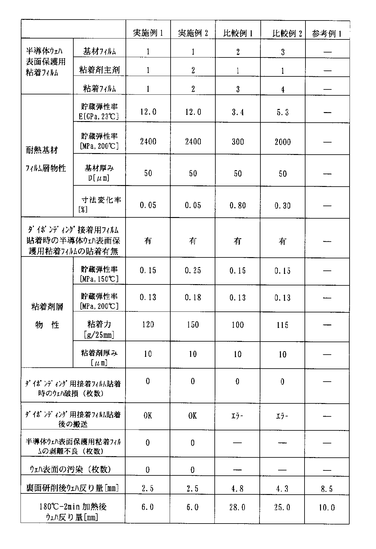
半導体ウェハ(PIウェハ)に対する、半導体ウェハ表面保護用粘着フィルム1の保護性能を評価した。半導体ウェハ表面保護用粘着フィルム1を集積回路が組み込まれた10枚のPIウェハ(直径:8インチ、厚み:750μm)の全表面に貼着した状態で、裏面研削機((株)ディスコ製、形式:DFG860)を用いて、厚みが100μmになるまでウェハ裏面を研削した。次いで、半導体ウェハ表面保護用粘着フィルム1を貼着したままの状態で、150℃においてダイボンディング用接着フィルム貼着機(タカトリ(株)製、形式:DM−800)を用いて、半導体ウェハ裏面にダイボンディング用接着フィルム(日立化成(株)製、商品名:ハイアタッチ)を貼着した。その結果、ダイボンディング用接着フィルム貼着機に内蔵するロールによってウェハに押圧がかかったにもかかわらず、10枚全ての半導体ウェハに対して接着フィルム貼着時においてPIウェハの反りが原因である割れは発生しなかった。また、ダイボンディング用接着フィルム貼付け後、チャックテーブルからアームによるウェハの搬送に問題は生じなかった。表1には、この現象をOKと記載した。更に、剥離機(日東精機(株)製、形式:HR8500II)を用いて、PIウェハ表面から半導体ウェハ表面保護用粘着フィルム1を剥離した。剥離の際においてもPIウェハの割れは発生しなかった。また、半導体ウェハ表面保護用粘着フィルム1を剥離した後のPIウェハ表面に糊残り等の汚染は観察されなかった。
別途、他のPIウェハ(直径:8インチ、厚み:750μm)10枚について上記と同様にして、厚みが100μmになるまでウェハ裏面を研削した後、半導体ウェハ表面保護用粘着フィルム1を貼着したままの状態で、反り量の測定を行った。その結果、半導体ウェハ表面保護用粘着フィルム貼付け面方向への反り量は2.5mmであった。さらに、ホットプレートを用いてPIウェハを180℃で2分間加熱し、加熱後の反り量を測定した。その結果、半導体ウェハ表面保護用粘着フィルム貼付け面方向への反り量は6.0mmであった。得られた結果を表1に示す。
【0057】
3−2.保護方法の実施例2
半導体ウェハ表面保護用粘着フィルム2を用いた以外、保護方法の実施例1と同様の方法を実施した。その結果、全ての評価で実施例1と同様の結果が得られた。得られた結果を表1に示す。
【0058】
3−3.保護方法の比較例1
半導体ウェハ表面保護用粘着フィルム3を用いた以外、保護方法の実施例1と同様の方法を実施した。その結果、ダイボンディング用接着フィルム貼付け時の熱によりウェハが大きく反ってしまい、チャックテーブルからアームによる搬送が吸着不良のため、10枚全てのPIウェハに於いて搬送することが出来なかった。表1には、この現象をエラーと記載した。裏面研削後のPIウェハの反り量は、半導体ウェハ表面保護用粘着フィルム貼付け面方向へ4.8mmであり、180℃で2分間加熱後の反り量は、半導体ウェハ表面保護用粘着フィルム貼付け面方向へ28.0mmであった。得られた結果を表1に示す。
【0059】
3−4.保護方法の比較例2
半導体ウェハ表面保護用粘着フィルム4を用いた以外、保護方法の実施例1と同様の方法を実施した。その結果、ダイボンディング用接着フィルム貼付け時の熱によりウェハが大きく反ってしまい、チャックテーブルからアームによる搬送が吸着不良のため、10枚全てのPIウェハに於いて搬送することが出来なかった。表1には、この現象をエラーと記載した。裏面研削後のPIウェハの反り量は、半導体ウェハ表面保護用粘着フィルム貼付け面方向へ4.3mmであり、180℃で2分間加熱後の反り量は半導体ウェハ表面保護用粘着フィルム貼付け面方向へ25.0mmであった。得られた結果を表1に示す。
【0060】
3−5.保護方法の参考例1
保護方法の実施例1と同様にして、PIウェハの裏面を研削した。次いで、PIウェハ表面から半導体ウェハ表面保護用粘着フィルム1を剥離した。粘着フィルム1を剥離した後、PIウェハの反りを測定したところ反り量は8.5mmであった。また、180℃で2分間加熱した後の反り量は10.0mmであった。
【0061】
【表1】
【発明の効果】
本発明によれば、厚みが100μm以下に薄層化され、且つ、ダイボンディング工程において高温に晒された場合であっても、半導体ウェハを製造する一連の工程における半導体ウェハの反りを矯正し、ウェハの破損、汚染などを防止することができる。[0001]
BACKGROUND OF THE INVENTION
The present invention relates to an adhesive film for protecting a semiconductor wafer surface, and a method for processing a back surface of a semiconductor wafer using the adhesive film for protecting a semiconductor wafer surface. Specifically, a pressure-sensitive adhesive film for protecting a semiconductor wafer surface used for processing the other surface of the wafer by sticking a pressure-sensitive adhesive film to the surface on which the integrated circuit of the semiconductor wafer such as silicon or gallium-arsenide is formed, The present invention also relates to a semiconductor wafer back surface processing method using the semiconductor wafer surface protecting adhesive film. More specifically, for semiconductor wafer surface protection that is suitable for preventing damage to semiconductor wafers and improving productivity in the manufacturing process of thinned semiconductor chips, particularly during back surface processing, adhesive film peeling, and transport operations. The present invention relates to an adhesive film and a method for processing a back surface of a semiconductor wafer using the adhesive film.
[0002]
[Prior art]
The process of processing a semiconductor wafer includes the steps of attaching a semiconductor wafer surface protective adhesive film to the circuit forming surface of the semiconductor wafer, processing the circuit non-forming surface of the semiconductor wafer, and peeling the semiconductor wafer surface protective adhesive film. After the process, the dicing process for dividing and cutting the semiconductor wafer, the die bonding process for bonding the divided semiconductor chip to the lead frame, and the molding process for sealing the semiconductor chip with resin for external protection, etc. Yes.
[0003]
Conventionally, in the die bonding process, a method in which a resin paste, which is a die bonding material, is supplied onto a lead frame, and a semiconductor chip is mounted thereon and bonded is most often used. However, when the resin paste is used, it is difficult to apply the resin paste uniformly on the lead frame, so that there are problems such as generation of voids and chip cracks when the adhesive layer is cured.
[0004]
JP-A-6-302629 discloses an adhesive film for die bonding in the die bonding process for the purpose of improving the non-uniform coating property, which is a defect of the resin paste that is a die bonding material, and rationalizing the overall process. A method of using is disclosed. This method includes a step of adhering an adhesive film for die bonding to a circuit non-formation surface of a semiconductor wafer, a dicing step of dividing and cutting the semiconductor wafer in a state of adhering the adhesive film for die bonding to a dicing tape, And a step of die bonding the semiconductor chip to the lead frame after the step of peeling the dicing tape.
[0005]
However, in this method, when the non-circuit-formed surface of the semiconductor wafer is processed to further reduce the thickness of the semiconductor wafer, particularly when the thickness is 100 μm or less, the semiconductor wafer surface protecting adhesive film is not attached. When sticking an adhesive film for die bonding, serious problems occur such as damage to the semiconductor wafer due to roll pressure, warpage of the wafer caused by thinning the wafer, and the like.
In recent years, the demand for thinner semiconductor chips is increasing, and a chip having a thickness of about 30 to 100 μm is also desired. Therefore, there is a demand for a method for protecting a semiconductor wafer in which a die bonding pressure-sensitive adhesive film can be adhered without damaging the thinned semiconductor wafer.
[0006]
[Problems to be solved by the invention]
In view of the above problems, the object of the present invention is to correct the warpage of the semiconductor wafer and damage it even when the semiconductor wafer is thinned to a thickness of about 100 μm or less and exposed to a high temperature in the die bonding process. An object of the present invention is to provide an adhesive film for protecting a surface of a semiconductor wafer, and a method for protecting a semiconductor wafer using the adhesive film.
[0007]
[Means for Solving the Problems]
As a result of intensive studies, the present inventors have paid attention to the thermal expansion coefficient, melting point, and storage elastic modulus of the base film of the semiconductor wafer surface protecting pressure-sensitive adhesive film, and have at least one layer of a resin having these specific characteristics. It discovered that the said subject could be solved by using for a film, and came to this invention.
That is, the present invention is a pressure-sensitive adhesive film for protecting a semiconductor wafer surface in which a pressure-sensitive adhesive layer is formed on one surface of a base film, and the dimensional change rate at 0 to 200 ° C. is ± 0 in at least one layer of the base film. It is related with the adhesive film for surface protection of a semiconductor wafer characterized by including the resin layer (A) which is less than 1%, and whose melting | fusing point is at least 200 degreeC and whose thickness is 10-300 micrometers.
Furthermore, the storage elastic modulus at 23 to 200 ° C. of at least one layer of the base film is at least 1 × 10 6.8It is Pa, It is related with the said adhesive film for semiconductor wafer surface protection characterized by the above-mentioned.
[0008]
In another aspect of the present invention, a first step of sticking a semiconductor wafer surface protecting adhesive film to a circuit forming surface of a semiconductor wafer, a second step of processing a circuit non-forming surface of a semiconductor wafer, and a semiconductor wafer A method for protecting a semiconductor wafer in a step including a third step of adhering an adhesive film for die bonding to a non-circuit-formed surface, wherein the third step is carried out without peeling off the adhesive film for protecting the semiconductor wafer surface, and The semiconductor wafer protecting method is characterized in that the semiconductor wafer surface protecting adhesive film is used as the semiconductor wafer surface protecting adhesive film.
By using the adhesive film for protecting the surface of a semiconductor wafer according to the present invention, in the back grinding process of the semiconductor wafer, the wafer in which the integrated circuit is protected by the protective film is thinned until the thickness becomes 100 μm or less, and Even when exposed to high temperatures in the die bonding process, the warpage of the semiconductor wafer is corrected by suppressing the dimensional change caused by the thermal expansion of the base film when the adhesive film for protecting the surface of the semiconductor wafer is heated. The wafer can be prevented from being damaged.
[0009]
DETAILED DESCRIPTION OF THE INVENTION
Hereinafter, the present invention will be described in detail. First, the adhesive film for protecting the surface of a semiconductor wafer according to the present invention will be described.
The adhesive film for protecting a semiconductor wafer surface according to the present invention is produced by forming an adhesive layer on one surface of a base film. Usually, in order to protect an adhesive layer, a peeling film is stuck on the surface of an adhesive layer. In consideration of sticking to the surface of the semiconductor wafer through the surface of the adhesive layer exposed when the release film is peeled off, in order to prevent contamination of the semiconductor wafer surface by the adhesive layer, on one side of the release film A method is preferred in which a pressure-sensitive adhesive coating solution is applied and dried to form a pressure-sensitive adhesive layer, and then the resulting pressure-sensitive adhesive layer is transferred to one side of a substrate film.
[0010]
The base film used for the adhesive film according to the present invention is characterized in that the dimensional change rate at 0 to 200 ° C. is within ± 0.1%, preferably within ± 0.05%, and the melting point is at least 200 ° C. And having at least one resin layer (A) having a thickness of 10 to 300 μm. The thickness of the entire base film is preferably 30 to 350 μm, more preferably 50 to 300 μm.
The resin layer has the effect of minimizing the stress of the pressure-sensitive adhesive film generated during and after heating and minimizing the amount of wafer warp deformation after heating.
[0011]
A liquid crystal polymer is mentioned as resin which forms the said resin layer (A). Examples of commercially available liquid crystal polymers include Kuraray Co., Ltd., trade name: Vecstar, Japan Gore-Tex Co., Ltd., trade name: BIAC (R). The liquid crystal polymer used in the present invention is generally composed of hydroxycarboxylic acid, aromatic dicarboxylic acid, and aromatic diol. The main chain skeleton is a benzene ring or a naphthalene ring and is excellent in thermal decomposition resistance. Therefore, a liquid crystal polymer having a higher aromatic ring ratio has higher flame retardancy. Further, by controlling the orientation, it is possible to control the thermal deformation start temperature and the thermal expansion coefficient. Furthermore, since it has high crystallinity, it exhibits excellent chemical resistance, is resistant to organic solvents, cleaning liquids, oils and glues, and is resistant to acids. In addition to the fact that the polymer molecule does not contain any water-affinity hydroxyl group or the like, the molecules are closely aligned like crystals, and the molecule is rigid, so it has excellent hygroscopic dimensional stability.
[0012]
Furthermore, the storage elastic modulus at 23 to 200 ° C. of at least one layer of the base film is at least 1 × 10 6.8Pa, more preferably 1 × 10⁹A high elastic modulus resin layer of Pa or higher is preferable. It is also possible for the resin layer (A) to have the characteristics of a high elastic modulus resin layer. The storage elastic modulus at 23 to 200 ° C. of at least one layer of the base film is 1 × 10⁸If it is less than Pa, in the step of attaching the adhesive film for die bonding, the surface protective adhesive film is melted by the heat and the base film in contact with the chuck table is melted, causing a problem in conveyance from the chuck table by the arm. Sometimes. Further, due to the warpage of the thinned semiconductor wafer, problems such as wafer breakage at the time of adhering the die bonding adhesive film and suction failure at the time of conveyance from the chuck table by the arm may occur. The thickness of the high elastic modulus resin layer is preferably 10 to 150 μm. More preferably, it is 30-130 micrometers. When the thickness exceeds 150 μm, the adhesive film may be attached to the semiconductor wafer and cutting failure may occur when cutting along the outer periphery of the semiconductor wafer. Moreover, the peeling defect of an adhesive film by the increase in bending stress may generate | occur | produce.
[0013]
Moreover, it is preferable to have a low elastic modulus resin layer. The low elastic modulus resin layer is a layer intended to absorb the uneven steps formed by the circuit on the surface of the semiconductor wafer due to its flexibility, and to prevent the semiconductor wafer from being damaged by the back surface grinding. From this viewpoint, the low elastic modulus resin layer has a storage elastic modulus at 23 ° C. of (E ′) 1 × 10⁵~ 1x10⁸Pa is preferred.
Examples of the resin capable of forming the low elastic modulus resin layer having the above characteristics include ethylene-vinyl acetate copolymer, ethylene-alkyl acrylate copolymer (alkyl group having 1 to 4 carbon atoms) and the like. Of these, ethylene-vinyl acetate copolymer is preferred. More preferred is ethylene-vinyl acetate copolymer having a vinyl acetate unit content of about 5 to 50% by weight.
[0014]
The pressure-sensitive adhesive forming the pressure-sensitive adhesive layer of the semiconductor wafer surface protecting pressure-sensitive adhesive film according to the present invention functions sufficiently as a pressure-sensitive adhesive even at a temperature of about 150.degree. It is preferable that Specifically, an acrylic adhesive, a silicon adhesive, etc. are illustrated. The thickness of the pressure-sensitive adhesive layer is preferably 3 to 100 μm. The pressure-sensitive adhesive layer preferably does not cause contamination due to adhesive residue or the like on the surface of the semiconductor wafer after the pressure-sensitive adhesive film for protecting the semiconductor wafer surface is peeled off from the circuit forming surface (hereinafter referred to as the surface) of the wafer.
[0015]
In particular, the pressure-sensitive adhesive layer prevents the adhesive force from becoming excessively large when exposed to a high temperature of about 150 ° C. in the die bonding process in which the adhesive film for die bonding is heated and adhered. In order not to increase, it is preferably one that has been crosslinked with high density by a crosslinking agent having a reactive functional group, a peroxide, radiation, or the like. Furthermore, even when the adhesive film for die bonding is stuck, even if it is heat-treated at a temperature of 150 ° C. or higher, the adhesive force will not increase and no peeling failure will occur, and adhesive residue will occur. Preferably not. Therefore, the adhesive layer has a storage elastic modulus at 150 ° C. of at least 1 × 10.5Pa is preferred. The higher the storage elastic modulus, the better, but the upper limit is usually 1 × 10.8It is about Pa.
[0016]
As a method for forming the pressure-sensitive adhesive layer having the above characteristics, a method using an acrylic pressure-sensitive adhesive is exemplified. The pressure-sensitive adhesive layer is an acrylic pressure-sensitive adhesive that is a (meth) acrylic acid alkyl ester monomer unit, a monomer unit having a functional group capable of reacting with a crosslinking agent, and an emulsion polymerization copolymer each containing a specific amount of a bifunctional monomer unit, In addition, it is formed by using a solution or an emulsion liquid containing a cross-linking agent having two or more functional groups in one molecule for increasing the cohesive force or adjusting the adhesive force. When used as a solution, the acrylic pressure-sensitive adhesive is separated from the emulsion liquid obtained by emulsion polymerization by salting out, etc., and then re-dissolved with a solvent or the like. Since acrylic pressure-sensitive adhesive has a sufficiently large molecular weight and low solubility in a solvent or often does not dissolve, it is preferable to use the emulsion liquid as it is from the viewpoint of cost.
As the acrylic pressure-sensitive adhesive used in the present invention, an acrylic acid alkyl ester, a methacrylic acid alkyl ester, or a mixture thereof is used as a main monomer [hereinafter referred to as monomer (A)], and a comonomer having a functional group capable of reacting with a crosslinking agent is used. The thing obtained by copolymerizing the monomer mixture containing is mentioned.
[0017]
Examples of the monomer (A) include an alkyl acrylate ester having an alkyl group having about 1 to 12 carbon atoms, or an alkyl methacrylate ester (hereinafter collectively referred to as (meth) acrylic acid alkyl ester). Preferably, it is a (meth) acrylic acid alkyl ester having an alkyl group having 1 to 8 carbon atoms. Specific examples include methyl acrylate, methyl methacrylate, ethyl acrylate, ethyl methacrylate, butyl acrylate, butyl methacrylate, and 2-ethylhexyl acrylate. These may be used alone or in combination of two or more. The amount of the monomer (A) used is usually preferably in the range of 10 to 98.9% by weight in the total amount of all monomers used as the raw material for the pressure-sensitive adhesive. More preferably, it is 85-95 weight%. By making the usage-amount of a monomer (A) into this range, the polymer containing 10-98.9 weight% of (meth) acrylic-acid alkylester monomer units (A), Preferably 85-95 weight% is obtained.
[0018]
As the monomer (B) that forms the monomer unit (B) having a functional group capable of reacting with a crosslinking agent, acrylic acid, methacrylic acid, itaconic acid, mesaconic acid, citraconic acid, fumaric acid, maleic acid, monoalkyl itaconic acid Ester, mesaconic acid monoalkyl ester, citraconic acid monoalkyl ester, fumaric acid monoalkyl ester, maleic acid monoalkyl ester, glycidyl acrylate, glycidyl methacrylate, 2-hydroxyethyl acrylate, 2-hydroxyethyl methacrylate, Examples include acrylamide, methacrylamide, tertiary-butylaminoethyl acrylate, and tertiary-butylaminoethyl methacrylate. Acrylic acid, methacrylic acid, 2-hydroxyethyl acrylate, 2-hydroxyethyl methacrylate, acrylamide, methacrylamide and the like are preferable. One of these may be copolymerized with the main monomer, or two or more may be copolymerized. It is preferable that the usage-amount of the monomer (B) which has a functional group which can react with a crosslinking agent is normally contained in 1-40 weight% in the total amount of all the monomers used as the raw material of an adhesive. More preferably, it is 1 to 10% by weight. Thus, a polymer having the structural unit (B) having a composition almost equal to the monomer composition is obtained.
[0019]
Furthermore, the pressure-sensitive adhesive layer preferably adjusts the adhesive force and peelability so that it functions sufficiently as a pressure-sensitive adhesive even under temperature conditions such as when processing the back surface of a semiconductor wafer and when attaching an adhesive film for die bonding. . As a measure therefor, it is preferable to consider a particle bulk crosslinking method in order to maintain the cohesive strength of the emulsion particles.
[0020]
For emulsion particles, 1 × 10 even under temperature conditions of 150-200 ° C.5In order to have Pa or more, it is preferable to improve the crosslinking method so as to maintain the cohesive force by copolymerizing the bifunctional monomer (C). Monomers that are well copolymerized include allyl methacrylate, allyl acrylate, divinylbenzene, vinyl methacrylate, vinyl acrylate, and, for example, diacrylate or dimethacrylate at both ends and the main chain structure is a propylene glycol type [NIPPON OIL Product name: PDP-200, PDP-400, ADP-200, ADP-400], tetramethylene glycol type [manufactured by NOF Corporation, product name: ADT-250, ADT- 850] and mixed types thereof (manufactured by NOF Corporation, trade names: ADET-1800, ADPT-4000).
[0021]
When the bifunctional monomer (C) is emulsion-copolymerized, the amount used is preferably 0.1 to 30% by weight in all monomers. More preferably, it is 0.1 to 5% by weight. Thus, a polymer having the structural unit (C) having a composition almost equal to the monomer composition is obtained.
In addition to the main monomer composing the pressure-sensitive adhesive and the comonomer having a functional group capable of reacting with the crosslinking agent, a specific comonomer having a property as a surfactant (hereinafter referred to as a polymerizable surfactant) is copolymerized. May be. The polymerizable surfactant has a property of copolymerizing with a main monomer and a comonomer, and also has an action as an emulsifier when emulsion polymerization is performed. In the case of using an acrylic pressure-sensitive adhesive that is emulsion-polymerized using a polymerizable surfactant, the surface of the semiconductor wafer is usually not contaminated by the surfactant. Even when slight contamination due to the pressure-sensitive adhesive layer occurs, it can be easily removed by washing the surface of the semiconductor wafer with water.
[0022]
Examples of such polymerizable surfactants include, for example, those obtained by introducing a polymerizable 1-propenyl group into the benzene ring of polyoxyethylene nonylphenyl ether [Daiichi Kogyo Seiyaku Co., Ltd .; trade name: Aqualon RN-10, RN-20, RN-30, RN-50, etc.], a polyoxyethylene nonylphenyl ether sulfate ester ammonium salt introduced with a polymerizable 1-propenyl group in the benzene ring Manufactured by Ichi Kogyo Seiyaku Co., Ltd .; trade names: Aqualon HS-10, HS-20, etc.], and sulfosuccinic acid diester type having a polymerizable double bond in the molecule [manufactured by Kao Corporation; trade name: Latemul S-120A, S-180A, etc.]. Further, if necessary, a monomer having a polymerizable double bond such as vinyl acetate, acrylonitrile, or styrene may be copolymerized.
[0023]
Examples of the polymerization reaction mechanism of the acrylic pressure-sensitive adhesive include radical polymerization, anionic polymerization, and cationic polymerization. Polymerization by radical polymerization is preferable in consideration of the production cost of the pressure-sensitive adhesive, the influence of the functional group of the monomer, the influence of ions on the surface of the semiconductor wafer, and the like. When polymerizing by radical polymerization reaction, organic compounds such as benzoyl peroxide, acetyl peroxide, isobutyryl peroxide, octanoyl peroxide, di-tertiary-butyl peroxide, di-tertiary-amyl peroxide as radical polymerization initiators Inorganic peroxides such as peroxide, ammonium persulfate, potassium persulfate, sodium persulfate, 2,2′-azobisisobutyronitrile, 2,2′-azobis-2-methylbutyronitrile, 4,4 Examples include azo compounds such as' -azobis-4-cyanovaleric acid.
[0024]
In the case of polymerization by emulsion polymerization method, among these radical polymerization initiators, inorganic peroxides such as water-soluble ammonium persulfate, potassium persulfate, and sodium persulfate, and water-soluble 4,4′-azobis are also used. An azo compound having a carboxyl group in the molecule such as -4-cyanovaleric acid is preferred. Considering the influence of ions on the surface of the semiconductor wafer, azo compounds having a carboxyl group in the molecule such as ammonium persulfate and 4,4'-azobis-4-cyanovaleric acid are more preferable. An azo compound having a carboxyl group in the molecule such as 4,4'-azobis-4-cyanovaleric acid is particularly preferable.
[0025]
The cross-linking agent having two or more cross-linkable functional groups used in the present invention is used for adjusting the adhesive force and cohesive force by reacting with the functional group of the acrylic pressure-sensitive adhesive. As crosslinking agents, epoxy compounds such as sorbitol polyglycidyl ether, polyglycerol polyglycidyl ether, pentaerythritol polyglycidyl ether, diglycerol polyglycidyl ether, glycerol polyglycidyl ether, neopentyl glycol diglycidyl ether, resorcin diglycidyl ether, etc. , Tetramethylene diisocyanate, hexamethylene diisocyanate, trimethylolpropane toluene diisocyanate triadduct, isocyanate compounds such as polyisocyanate, trimethylolpropane-tri-β-aziridinyl propionate, tetramethylolmethane-tri-β- Aziridinyl propionate, N, N′-diphenylmethane-4,4′-bis (1-aziridinecarboxyl ), N, N′-hexamethylene-1,6-bis (1-aziridinecarboxamide), N, N′-toluene-2,4-bis (1-aziridinecarboxamide), trimethylolpropane-tri- of aziridine compounds such as β- (2-methylaziridine) propionate, N, N, N ′, N′-tetraglycidyl m-xylenediamine, 1,3-bis (N, N′-diglycidylaminomethyl) cyclohexane Examples include tetrafunctional epoxy compounds and melamine compounds such as hexamethoxymethylol melamine. These may be used alone or in combination of two or more.
[0026]
In general, the content of the crosslinking agent is preferably in a range in which the number of functional groups in the crosslinking agent does not exceed the number of functional groups in the acrylic pressure-sensitive adhesive. However, when a functional group is newly generated by the crosslinking reaction, or when the crosslinking reaction is slow, it may be contained excessively as necessary. A preferable content is 0.1 to 15 parts by weight of a crosslinking agent with respect to 100 parts by weight of the acrylic pressure-sensitive adhesive. When the content is too small, the cohesive force of the pressure-sensitive adhesive layer becomes insufficient, and the elastic modulus is 1 × 10 at 150 to 200 ° C.5It becomes less than Pa, and the heat resistance is reduced. For this reason, adhesive residue due to the pressure-sensitive adhesive layer is likely to be generated, and the adhesive strength is increased. When the surface-protective pressure-sensitive adhesive film is peeled off from the surface of the semiconductor wafer, a peeling trouble occurs with the automatic peeling machine. It may be completely damaged. If the content is too high, the adhesive force between the adhesive layer and the surface of the semiconductor wafer will be weakened, and in the semiconductor wafer back grinding process, polishing scrapes will invade between the semiconductor wafer surface and the adhesive layer and damage the semiconductor wafer. Or may contaminate the surface of the semiconductor wafer.
[0027]
In addition to the acrylic adhesive and the crosslinking agent copolymerized with the specific bifunctional monomer, the adhesive coating liquid used in the present invention is a tackifier such as rosin or terpene resin to adjust the adhesive properties. Various surfactants and the like may be appropriately contained to such an extent that the object of the present invention is not affected. When the coating solution is an emulsion solution, a film-forming aid such as diethylene glycol monoalkyl ether may be added as appropriate so as not to affect the purpose of the present invention. Diethylene glycol monoalkyl ether and derivatives thereof used as a film-forming aid may contaminate the surface of the semiconductor wafer to such an extent that it cannot be cleaned when present in a large amount in the pressure-sensitive adhesive layer. For this reason, it is preferable to use one that has a property of volatilizing at the drying temperature of the pressure-sensitive adhesive coating solution, and to reduce the residual amount in the pressure-sensitive adhesive layer as much as possible.
[0028]
The adhesive strength of the adhesive film for protecting a semiconductor wafer surface of the present invention is appropriately adjusted in consideration of the processing conditions of the semiconductor wafer, the diameter of the semiconductor wafer, the thickness of the semiconductor wafer after back grinding, the temperature for attaching the adhesive film for die bonding, etc. it can. If the adhesive strength is too low, it will be difficult to attach the surface protective adhesive film to the surface of the semiconductor wafer, the protective performance of the surface protective adhesive film will be insufficient, the semiconductor wafer will be damaged, Contamination due to grinding scraps may occur. Also, if the adhesive strength is too high, after performing the backside processing of the semiconductor wafer, when the surface protective adhesive film is peeled off from the semiconductor wafer surface, a peeling trouble may occur with an automatic peeling machine, etc. Or the semiconductor wafer may be damaged. Usually, it is 5 to 500 g / 25 mm, preferably 10 to 300 g / 25 mm, in terms of adhesive strength to the SUS304-BA plate.
[0029]
As a method of applying a pressure-sensitive adhesive coating solution to one surface of a base film or a release film, a conventionally known coating method such as a roll coater method, a reverse roll coater method, a gravure roll method, a bar coat method, a comma coater method, A die coater method or the like can be adopted. Although there is no restriction | limiting in particular in the drying conditions of the apply | coated adhesive, Generally, it is preferable to dry for 10 second-10 minutes in the temperature range of 80-200 degreeC. More preferably, it is dried at 80 to 170 ° C. for 15 seconds to 5 minutes. In order to sufficiently accelerate the crosslinking reaction between the crosslinking agent and the pressure-sensitive adhesive, the surface protective pressure-sensitive adhesive film may be heated at 40 to 80 ° C. for about 5 to 300 hours after the drying of the pressure-sensitive adhesive coating solution is completed.
[0030]
The manufacturing method of the adhesive film for protecting a semiconductor wafer surface of the present invention is as described above. From the viewpoint of preventing contamination of the surface of the semiconductor wafer, the manufacturing environment for all raw materials such as a base film, a release film, and an adhesive main agent is used. The preparation, storage, application and drying environment of the adhesive coating solution are preferably maintained at a cleanness of class 1,000 or less as defined in the US Federal Standard 209b.
The semiconductor wafer manufacturing method to which the semiconductor wafer protection method according to the present invention is applied is as follows. First, as described above, the first step of adhering the semiconductor wafer surface protection adhesive film to the surface of the semiconductor wafer, The second step of processing the forming surface (hereinafter referred to as the back surface) is sequentially performed, and then the third step of adhering the die bonding adhesive film to the back surface of the semiconductor wafer without peeling off the surface protective adhesive film. To implement. There are no particular restrictions on the subsequent steps, for example, a step of peeling the semiconductor wafer surface protective adhesive film, a dicing step of dividing and cutting the semiconductor wafer, a molding step of sealing the semiconductor chip with a resin for external protection, etc. A method for manufacturing a semiconductor wafer in which the steps are sequentially performed.
[0031]
The semiconductor wafer protection method of the present invention will be described in detail. The semiconductor wafer protection method of the present invention sequentially performs a first step of sticking a semiconductor wafer surface protective adhesive film on the surface of the semiconductor wafer and a second step of processing the back surface of the semiconductor wafer, and subsequently the semiconductor wafer surface. The 3rd process of sticking the adhesive film for die bonding on the back of a semiconductor wafer is carried out, without peeling off the protective adhesive film. At this time, the semiconductor wafer surface protecting adhesive film is used as the semiconductor wafer surface protecting adhesive film.
[0032]
For details of the method for protecting a semiconductor wafer according to the present invention, first, the release film is peeled from the pressure-sensitive adhesive layer side of the pressure-sensitive adhesive film for semiconductor wafer surface protection (hereinafter abbreviated as surface protective pressure-sensitive film), and the surface of the pressure-sensitive adhesive layer is removed. An adhesive film for surface protection is attached to the surface of the semiconductor wafer through the adhesive layer (first step). Next, the semiconductor wafer is fixed to the chuck table or the like of the back surface processing machine via the base film layer of the surface protecting adhesive film, and the back surface of the semiconductor wafer is processed (second step). In the second step, all of the backside grinding step, wet etching step, and polishing step of the semiconductor wafer may be performed, or any one of these steps may be performed. Next, the adhesive film for surface bonding is transported to the bonding process of the adhesive film for die bonding without peeling off the adhesive film for surface protection, and the adhesive film for die bonding is bonded (third process). Thereafter, the surface protecting adhesive film is peeled off. Moreover, after peeling the surface-protective adhesive film as necessary, the semiconductor wafer surface is subjected to treatment such as water washing and plasma washing.
[0033]
Conventionally, in the back surface processing step, a semiconductor wafer having a thickness of 500 to 1000 μm before grinding is ground and thinned to about 200 to 600 μm depending on the type of semiconductor chip and the like. On the other hand, by applying the protection method of the present invention, the thickness can be reduced until the thickness becomes 100 μm or less. In that case, the minimum thickness of the semiconductor wafer is about 20 μm. When the thickness is reduced to 100 μm or less, a wet etching process or a polishing process can be performed subsequent to the back surface grinding. The thickness of the semiconductor wafer before grinding the back surface is appropriately determined depending on the diameter and type of the semiconductor wafer, and the thickness of the semiconductor wafer after the back surface grinding is appropriately determined depending on the size of the chip to be obtained, the type of circuit, and the like.
The operation of adhering the surface protective adhesive film to the surface of the semiconductor wafer may be performed manually, but is generally performed by an apparatus called an automatic attaching machine equipped with a roll-shaped surface protective adhesive film. . Examples of such an automatic pasting machine include Takatori Co., Ltd., model: ATM-1000B, ATM-1100, TEAM-100, Teikoku Seiki Co., Ltd., model: STL series.
[0034]
As the back surface grinding method, a known grinding method such as a through-feed method or an in-feed method is employed. In either method, back surface grinding is usually performed while supplying water to the semiconductor wafer and the grindstone and cooling. After the back surface grinding, wet etching and polishing are performed as necessary. The wet etching process and the polishing process are performed for the purpose of removing strain generated on the back surface of the semiconductor wafer, further thinning the semiconductor wafer, removing an oxide film, etc., pretreatment when forming electrodes on the back surface. The etching solution is appropriately selected according to the above purpose.
[0035]
As an apparatus used at the process of sticking the adhesive film for die-bonding, Takatori Co., Ltd. make and format: DM-800 etc. are mentioned, for example. Examples of the adhesive film for die bonding include an adhesive film for die bonding in which a varnish made of a mixture of a polyimide resin and a thermosetting resin is applied to the surface of a polyester or polypropylene film to form an adhesive layer. At this time, an additive may be mixed with the mixture of a polyimide resin and a thermosetting resin as needed. By using a roll, the adhesive film for die bonding is heated and pasted to the back surface of the semiconductor wafer to obtain a semiconductor wafer with an adhesive.
[0036]
Usually, when adhering an adhesive film for die bonding to the back surface of a semiconductor wafer, an adhesive film adhering apparatus for die bonding as described above is used. It is heated to about 150 ° C. and pressed by a roll built in the apparatus, and an adhesive film for die bonding is attached to the back surface of the semiconductor wafer. At this time, if there is a large warp in the thinned wafer, the wafer is easily damaged by the pressing of the roll. In addition, even if the die bonding adhesive film can be adhered to the back side of the semiconductor wafer without damaging the wafer, problems such as poor suction at the time of conveyance from the chuck table by the arm will occur if the wafer is greatly warped.
[0037]
By sticking the adhesive film according to the present invention to the wafer surface to make the wafer thin, and by sticking the adhesive film for die bonding without peeling off the adhesive film, the warpage of the wafer is corrected and the damage In addition, poor conveyance can be prevented.
[0038]
After the back grinding process, the etching process, and the bonding process of the die bonding adhesive film are finished, the surface protecting adhesive film is peeled off from the surface of the semiconductor wafer. Although a series of these operations may be performed manually, it is generally performed using an apparatus called an automatic peeling machine. Examples of such an automatic peeling machine include Takatori Co., Ltd., model: ATRM-2000B, ATRM-2100, Teikoku Seiki Co., Ltd., model: STP series. Moreover, it is preferable to heat-peel as needed for the purpose of improving peelability.
The surface of the semiconductor wafer after peeling off the surface protective adhesive film is cleaned as necessary. Examples of the cleaning method include wet cleaning such as water cleaning and solvent cleaning, and dry cleaning such as plasma cleaning. In the case of wet cleaning, ultrasonic cleaning may be used in combination. These cleaning methods are appropriately selected depending on the contamination state of the semiconductor wafer surface.
Semiconductor wafers to which the semiconductor wafer protection method of the present invention can be applied are not limited to silicon wafers, but include wafers of germanium, gallium-arsenic, gallium-phosphorus, gallium-arsenic-aluminum, and the like.
[0039]
【Example】
Hereinafter, the present invention will be described in more detail with reference to examples. In all examples and comparative examples shown below, preparation and application of an adhesive coating solution in an environment maintained at a cleanness of class 1,000 or less as defined in US Federal Standard 209b, backside grinding of a semiconductor silicon wafer, In addition, manufacture of adhesive films for die bonding was carried out. The present invention is not limited to these examples. Various characteristic values shown in the examples were measured by the following methods.
[0040]
1. Measuring method of various characteristics
1-1. Adhesive strength measurement (g / 25mm)
Except for the conditions specified below, all measurements are performed in accordance with the method specified in JIS Z0237-1991. In an atmosphere of 23 ° C., the adhesive film obtained in Example or Comparative Example was stuck to the surface of a 20 cm × 5 cm rectangular SUS304-BA plate (JIS G4305-1991 regulation) through the adhesive layer. Cut the adhesive film to the same size and leave it for 60 minutes. However, the adhesive film has a machine direction (hereinafter referred to as MD direction) of 20 cm side of the SUS304-BA plate and a direction orthogonal to the machine direction (hereinafter referred to as TD direction) to the 5 cm side of the SUS304-BA plate. Adhere the adhesive film. One end of the sample in the MD direction is sandwiched, the peeling angle is 180 degrees, and the peeling speed is 300 mm / min. Then, the stress at the time of peeling the sample from the surface of the SUS304-BA plate is measured and converted to a width of 25 mm.
[0041]
1-2. Storage modulus (Pa)
1) Adhesive layer
The adhesive layer portion of the adhesive film for protecting a semiconductor wafer surface is laminated so as to have a thickness of 1 mm, and a viscoelasticity measurement sample having a diameter of 8 mm is prepared. The storage elastic modulus is measured at 150 ° C. and 200 ° C. using a dynamic viscoelasticity measuring device (Rheometrics: model: RMS-800). The measurement frequency is 1 Hz and the distortion is 0.1 to 3%.
2) Base film layer
The base film layer part of the adhesive film for protecting a semiconductor wafer surface is cut to produce a rectangular (MD direction: 30 mm, TD direction: 10 mm) sample. The storage elastic modulus (machine direction) from 0 to 300 ° C. is measured using a dynamic viscoelasticity measuring device (Rheometrics: model: RSA-II). The measurement frequency is 1 Hz, and the distortion is 0.01 to 0.1%. However, in the case of a laminated substrate film, the measurement was performed independently for each layer.
[0042]
1-3. Dimensional change rate of base film (%)
A base film is cut into a square (MD direction: 30 cm, TD direction: 30 cm), and a spot (MD direction: 25 cm, TD direction: 25 cm) is opened on the base film with a punch to prepare a sample. Using a two-dimensional measuring machine (manufactured by Mitutoyo Corporation: Model: CRYSTAL * μV606), the spot interval opened in the base film is measured. After the measurement, the sample is placed in a 200 ° C. oven. After 2 minutes, the sample is taken out of the oven, the spot interval is measured, and the dimensional change rate before and after heating is calculated in the MD direction and the TD direction. Based on the following formula, the heating dimensional change rate (%) in the MD direction and the TD direction is calculated. Measurement is performed on 10 samples, and an average value in the MD direction and the TD direction is set to a value having a larger absolute value as a dimensional change rate of the base film. However, L in the formula0Denotes a spot interval before heating, and L denotes a spot interval after heating.
Dimensional change rate (%) = 100 × (L−L0) / L0
1-4. Pollution assessment
A surface protective adhesive film for a sample is placed on the surface of 10 semiconductor silicon wafers (diameter: 8 inches, thickness: 600 μm, scribe line depth: 8 μm, scribe line width: 100 μm) through the adhesive layer. Adhering to the entire surface of the semiconductor silicon wafer, passing through the back surface processing process of the semiconductor wafer and the adhesive film attaching process for die bonding, and then using a peeling machine (manufactured by Nitto Seiki Co., Ltd., model: HR8500II) Then, the surface of the semiconductor wafer is observed at 250 magnifications using a laser focus microscope (manufactured by KEYENCE, model: VF-7510, VF-7500, VP-ED100). It shows the number of wafers on which the adhesive residue was recognized on the surface after the adhesive film was peeled off.
[0043]
1-5. Evaluation of semiconductor wafer warpage
A pressure-sensitive adhesive film for surface protection is applied to the surface of an 8-inch silicon wafer (hereinafter abbreviated as PI wafer, diameter: about 200 mm, thickness: 725 μm) having a polyimide film having a thickness of 10 μm disposed on the surface of the semiconductor wafer. Then, the wafer back surface is ground and thinned to a thickness of 100 μm using a back surface grinding machine (manufactured by DISCO Corporation, model: DFG860). After the thinning, the PI wafer is placed on the surface plate with the surface protective adhesive film affixing surface facing up in a state where the surface protective adhesive film is affixed to the surface of the PI wafer. The maximum distance between the surface plate and the wafer back surface is measured and used as the amount of warpage. Next, the PI wafer after thinning to which the adhesive film for surface protection was attached was heated at 180 ° C. for 2 minutes using a hot plate (manufactured by Advantech Co., Ltd., model: TP-320) in the same manner as above. The amount of warpage after heating is measured. Ten PI wafers were evaluated, and the average value is shown.
[0044]
1-6. Damage to semiconductor wafer (number)
The number of damaged semiconductor wafers in the semiconductor wafer back grinding process, the die bonding adhesive film attaching process, and the surface protecting adhesive film peeling process is shown. 10 PI wafers were evaluated and the number of damaged wafers is shown.
[0045]
2. Production example of adhesive film for surface protection
2-1. Production example 1 of base film
The rate of dimensional change when heat of 0 to 200 ° C. is applied is within ± 0.1%, the melting point is 200 ° C. or higher, and the storage elastic modulus at 23 ° C. to 200 ° C. is at least 1 × 10⁸As a resin that is Pa, a liquid crystal polymer film [manufactured by Kuraray Co., Ltd., trade name: Vecstar OC, thickness: 50 μm] was selected. The surface on the side where the pressure-sensitive adhesive layer is formed was subjected to corona treatment to obtain a base film 1. The dimensional change rate at 200 ° C. was 0.05%, the melting point was 310 ° C., and the storage elastic modulus was 12.0 GPa at 23 ° C. and 2.4 GPa at 200 ° C.
[0046]
2-2. Comparative production example 1 of base film
A biaxially stretched polyethylene terephthalate film [manufactured by Teijin Ltd., trade name: Tetoron, thickness: 50 μm] was used as the base film 2. The surface on the side where the pressure-sensitive adhesive layer is formed was subjected to corona discharge treatment. The dimensional change rate at 200 ° C. was 0.80%, the melting point was 258 ° C., and the storage elastic modulus was 3.4 GPa at 23 ° C. and 300 MPa at 200 ° C.
[0047]
2-3. Comparative production example 2 of base film
A biaxially stretched polyethylene naphthalate film [manufactured by Teijin Ltd., trade name: Teonex, thickness (D): 50 μm] was used as the base film 3. The surface on the side where the pressure-sensitive adhesive layer is formed was subjected to corona discharge treatment. The dimensional change rate at 200 ° C. was: 0.30%, the melting point was 269 ° C., and the storage elastic modulus was 5.3 GPa at 23 ° C. and 2000 MPa at 200 ° C.
[0048]
2-4. Production Example 1 of Adhesive Main Agent
In a polymerization reactor, 150 parts by weight of deionized water, 0.625 parts by weight of 4,4′-azobis-4-cyanovaleric acid [manufactured by Otsuka Chemical Co., Ltd., trade name: ACVA] as a polymerization initiator, monomer ( A) is 62.25 parts by weight of acrylic acid-2-ethylhexyl, 18 parts by weight of acrylic acid-n-butyl and 12 parts by weight of methyl methacrylate, and monomer (B) is 3 parts by weight of 2-hydroxyethyl methacrylate, methacrylic acid. 2 parts by weight of acid and 1 part by weight of acrylamide, 1 part by weight of polytetramethylene glycol diacrylate [manufactured by NOF Corporation, product name: ADT-250] as monomer (C), polyoxyethylene nonylphenyl as water-soluble comonomer Ammonium salt of sulfuric acid ester of ether (average number of moles of ethylene oxide added: about 20) A benzene ring having a polymerizable 1-propenyl group introduced therein [trade name: Aqualon HS-10, manufactured by Daiichi Kogyo Seiyaku Co., Ltd.] was charged in an amount of 0.75 part by weight, and the mixture was stirred at 70 to 72 ° C. Emulsion polymerization was carried out for 8 hours to obtain an acrylic resin emulsion. This was neutralized with 9% by weight aqueous ammonia (pH = 7.0) to obtain an acrylic pressure-sensitive adhesive (pressure-sensitive adhesive main agent 1) having a solid content of 42.5% by weight.
[0049]
2-5. Production example 2 of adhesive main agent
In a polymerization reactor, 150 parts by weight of deionized water, 0.625 parts by weight of 4,4′-azobis-4-cyanovaleric acid [manufactured by Otsuka Chemical Co., Ltd., trade name: ACVA] as a polymerization initiator, monomer ( A) is 62.25 parts by weight of acrylic acid-2-ethylhexyl, 18 parts by weight of acrylic acid-n-butyl and 12 parts by weight of methyl methacrylate, and monomer (B) is 3 parts by weight of 2-hydroxyethyl methacrylate, methacrylic acid. 2 parts by weight of acid, 1 part by weight of acrylamide, 1 part by weight of allyl methacrylate (manufactured by Wako Pure Chemical Industries, Ltd.) as monomer (C), polyoxyethylene nonylphenyl ether (addition moles of ethylene oxide) as water-soluble comonomer Average value: about 20) Introducing a polymerizable 1-propenyl group into the benzene ring of the ammonium salt of sulfate ester 0.75 parts by weight (product name: Aqualon HS-10, manufactured by Daiichi Kogyo Seiyaku Co., Ltd.) was charged, and emulsion polymerization was carried out at 70 to 72 ° C. for 8 hours with stirring, and an acrylic resin emulsion Got. This was neutralized with 9% by weight aqueous ammonia (pH = 7.0) to obtain an acrylic pressure-sensitive adhesive (pressure-sensitive adhesive main agent 2) having a solid content of 42.5% by weight.
[0050]
2-6. Production example 1 of adhesive coating solution
Production Example 1 of Adhesive Main Agent 100 parts by weight of the obtained Adhesive Main Agent 1 was collected and further adjusted to pH 9.5 by adding 9% by weight aqueous ammonia. Next, 1.6 parts by weight of an aziridine-based crosslinking agent [manufactured by Nippon Shokubai Chemical Industry Co., Ltd., trade name: Chemitite Pz-33] was added to obtain an adhesive coating solution 1.
[0051]
2-7. Production example 2 of adhesive coating solution
A pressure-sensitive adhesive coating solution 2 was obtained in the same manner as the pressure-sensitive adhesive coating solution Production Example 1 except that the pressure-sensitive adhesive main agent 2 obtained in Production Example 2 of the pressure-sensitive adhesive main agent was used.
[0052]
2-8. Production example 1 of adhesive film
The pressure-sensitive adhesive coating solution 1 was applied to a polypropylene film (release film, thickness: 50 μm) using a roll coater, and dried at 120 ° C. for 2 minutes to provide a pressure-sensitive adhesive layer having a thickness of 10 μm. The corona discharge-treated surface of the base film 1 was bonded and pressed on this to transfer the pressure-sensitive adhesive layer. After the transfer, the film was heated at 60 ° C. for 48 hours, and then cooled to room temperature to produce a semiconductor wafer surface protecting adhesive film 1. The storage elastic modulus of the adhesive layer is 1.5 × 10 5 at 150 ° C.5Pa, 1.3 × 10 at 200 ° C.5Pa. The adhesive strength was 120 g / 25 mm.
[0053]
2-9. Production example 2 of adhesive film
The pressure-sensitive adhesive coating liquid 2 was applied to a polypropylene film (release film, thickness: 50 μm) using a roll coater, and dried at 120 ° C. for 2 minutes to provide a pressure-sensitive adhesive layer having a thickness of 10 μm. The corona discharge-treated surface of the base film 1 was bonded and pressed on this to transfer the pressure-sensitive adhesive layer. After the transfer, the film was heated at 60 ° C. for 48 hours, and then cooled to room temperature to produce a semiconductor wafer surface protecting adhesive film 2. The storage elastic modulus of the pressure-sensitive adhesive layer is 2.5 × 10 5 at 150 ° C.5Pa, 1.8 × 10 at 200 ° C.5Pa. The adhesive strength was 150 g / 25 mm.
[0054]
2-10. Comparative production example 1 of adhesive film
A semiconductor wafer surface protective adhesive film 3 was produced in the same manner as in Production Example 1 of the adhesive film except that the base film 2 and the adhesive coating solution 1 were used. The storage elastic modulus of the adhesive layer is 1.5 × 10 5 at 150 ° C.5Pa, 1.3 × 10 at 200 ° C.5Pa. The adhesive strength was 100 g / 25 mm.
[0055]
2-11. Comparative production example 2 of adhesive film
A semiconductor wafer surface protecting adhesive film 4 was produced in the same manner as in Production Example 1 of the adhesive film except that the base film 3 and the adhesive coating solution 1 were used. The storage elastic modulus of the adhesive layer is 1.5 × 10 5 at 150 ° C.5Pa, 1.3 × 10 at 200 ° C.5Pa. The adhesive strength was 115 g / 25 mm.
[0056]
3-1. Example 1 of protection method
The protection performance of the adhesive film 1 for protecting a semiconductor wafer surface against a semiconductor wafer (PI wafer) was evaluated. In a state where the adhesive film 1 for protecting the surface of a semiconductor wafer is adhered to the entire surface of 10 PI wafers (diameter: 8 inches, thickness: 750 μm) in which integrated circuits are incorporated, a back grinding machine (manufactured by DISCO Corporation, Using the format: DFG860), the back surface of the wafer was ground until the thickness reached 100 μm. Next, with the adhesive film 1 for protecting the surface of the semiconductor wafer being adhered, the back surface of the semiconductor wafer was used at 150 ° C. using an adhesive film adhering machine for die bonding (manufactured by Takatori Corporation, model: DM-800). An adhesive film for die bonding (manufactured by Hitachi Chemical Co., Ltd., trade name: High Attach) was attached to the substrate. As a result, even when the wafer is pressed by the roll built in the die bonding adhesive film sticking machine, the PI wafer warpage is caused when the adhesive film is stuck to all ten semiconductor wafers. No cracking occurred. Further, there was no problem in transferring the wafer from the chuck table by the arm after the adhesive film for die bonding was attached. Table 1 described this phenomenon as OK. Furthermore, the adhesive film 1 for semiconductor wafer surface protection was peeled from the PI wafer surface using a peeling machine (Nitto Seiki Co., Ltd., model: HR8500II). Even during the peeling, the PI wafer was not cracked. Further, no contamination such as adhesive residue was observed on the PI wafer surface after the semiconductor wafer surface protecting adhesive film 1 was peeled off.
Separately, 10 other PI wafers (diameter: 8 inches, thickness: 750 μm) were ground in the same manner as described above, and the wafer back surface was ground until the thickness became 100 μm, and then the adhesive film 1 for protecting the semiconductor wafer surface was adhered. The amount of warpage was measured as it was. As a result, the amount of warpage in the direction of the semiconductor wafer surface protecting adhesive film attaching surface was 2.5 mm. Further, the PI wafer was heated at 180 ° C. for 2 minutes using a hot plate, and the amount of warpage after the heating was measured. As a result, the amount of warpage in the direction of the semiconductor wafer surface protecting adhesive film pasting surface was 6.0 mm. The obtained results are shown in Table 1.
[0057]
3-2. Example 2 of protection method
A method similar to Example 1 of the protection method was carried out except that the semiconductor wafer surface protecting adhesive film 2 was used. As a result, the same results as in Example 1 were obtained in all evaluations. The obtained results are shown in Table 1.
[0058]
3-3. Comparative example 1 of protection method
The same method as Example 1 of the protection method was carried out except that the semiconductor wafer surface protecting adhesive film 3 was used. As a result, the wafer was greatly warped by heat at the time of adhering the adhesive film for die bonding, and the transfer from the chuck table by the arm was poor, so that it could not be transferred on all 10 PI wafers. Table 1 describes this phenomenon as an error. The warpage amount of the PI wafer after back grinding is 4.8 mm in the direction of the adhesive surface for attaching the semiconductor wafer surface protection, and the warpage amount after heating at 180 ° C. for 2 minutes is in the direction of the adhesive surface for attaching the semiconductor wafer surface protection surface. It was 28.0 mm. The obtained results are shown in Table 1.
[0059]
3-4. Comparative example 2 of protection method
A method similar to Example 1 of the protection method was carried out except that the semiconductor wafer surface protecting adhesive film 4 was used. As a result, the wafer was greatly warped by heat at the time of adhering the adhesive film for die bonding, and the transfer from the chuck table by the arm was poor, so that it could not be transferred on all 10 PI wafers. Table 1 describes this phenomenon as an error. The warp amount of the PI wafer after back grinding is 4.3 mm in the direction of the adhesive surface for the semiconductor wafer surface protection, and the warpage amount after heating for 2 minutes at 180 ° C. is in the direction of the adhesive surface for the semiconductor wafer surface protection. It was 25.0 mm. The obtained results are shown in Table 1.
[0060]
3-5. Reference example 1 of protection method
The back surface of the PI wafer was ground in the same manner as in Example 1 of the protection method. Subsequently, the adhesive film 1 for protecting a semiconductor wafer surface was peeled from the surface of the PI wafer. After the adhesive film 1 was peeled off, the warpage of the PI wafer was measured and the amount of warpage was 8.5 mm. Further, the amount of warpage after heating at 180 ° C. for 2 minutes was 10.0 mm.
[0061]
[Table 1]
【The invention's effect】
According to the present invention, even when the thickness is reduced to 100 μm or less and the die bonding process is exposed to a high temperature, the warpage of the semiconductor wafer in a series of processes for manufacturing a semiconductor wafer is corrected, It is possible to prevent wafer breakage and contamination.
Claims (7)
Priority Applications (1)
| Application Number | Priority Date | Filing Date | Title |
|---|---|---|---|
| JP2003183637A JP2005019759A (en) | 2003-06-27 | 2003-06-27 | Semiconductor wafer surface protecting adhesive film and semiconductor wafer protecting method using the adhesive film |
Applications Claiming Priority (1)
| Application Number | Priority Date | Filing Date | Title |
|---|---|---|---|
| JP2003183637A JP2005019759A (en) | 2003-06-27 | 2003-06-27 | Semiconductor wafer surface protecting adhesive film and semiconductor wafer protecting method using the adhesive film |
Publications (1)
| Publication Number | Publication Date |
|---|---|
| JP2005019759A true JP2005019759A (en) | 2005-01-20 |
Family
ID=34183625
Family Applications (1)
| Application Number | Title | Priority Date | Filing Date |
|---|---|---|---|
| JP2003183637A Pending JP2005019759A (en) | 2003-06-27 | 2003-06-27 | Semiconductor wafer surface protecting adhesive film and semiconductor wafer protecting method using the adhesive film |
Country Status (1)
| Country | Link |
|---|---|
| JP (1) | JP2005019759A (en) |
Cited By (7)
| Publication number | Priority date | Publication date | Assignee | Title |
|---|---|---|---|---|
| JP2009253082A (en) * | 2008-04-08 | 2009-10-29 | Lintec Corp | Adhesive sheet for processing semiconductor wafer, method for adjusting semiconductor wafer processing device using the same, and evaluation method of adhesive sheet |
| JP2009253081A (en) * | 2008-04-08 | 2009-10-29 | Lintec Corp | Adhesive sheet for semiconductor wafer processing, adjustment method of semiconductor wafer processor using the same, and evaluation method of adhesive sheet |
| JP2010108995A (en) * | 2008-10-28 | 2010-05-13 | Lintec Corp | Sheet repasting device, and sheet repasting method |
| JP2010287836A (en) * | 2009-06-15 | 2010-12-24 | Hitachi Chem Co Ltd | Adhesive film laminate for semiconductor processing |
| JP2017054891A (en) * | 2015-09-08 | 2017-03-16 | 三井化学東セロ株式会社 | Film for manufacturing electronic component, electronic component and method for manufacturing the same |
| JP2019047075A (en) * | 2017-09-07 | 2019-03-22 | 日東電工株式会社 | Adhesive tape for semiconductor wafer protection |
| JP2020161823A (en) * | 2016-05-02 | 2020-10-01 | 日立化成株式会社 | How to process electronic components |
-
2003
- 2003-06-27 JP JP2003183637A patent/JP2005019759A/en active Pending
Cited By (7)
| Publication number | Priority date | Publication date | Assignee | Title |
|---|---|---|---|---|
| JP2009253082A (en) * | 2008-04-08 | 2009-10-29 | Lintec Corp | Adhesive sheet for processing semiconductor wafer, method for adjusting semiconductor wafer processing device using the same, and evaluation method of adhesive sheet |
| JP2009253081A (en) * | 2008-04-08 | 2009-10-29 | Lintec Corp | Adhesive sheet for semiconductor wafer processing, adjustment method of semiconductor wafer processor using the same, and evaluation method of adhesive sheet |
| JP2010108995A (en) * | 2008-10-28 | 2010-05-13 | Lintec Corp | Sheet repasting device, and sheet repasting method |
| JP2010287836A (en) * | 2009-06-15 | 2010-12-24 | Hitachi Chem Co Ltd | Adhesive film laminate for semiconductor processing |
| JP2017054891A (en) * | 2015-09-08 | 2017-03-16 | 三井化学東セロ株式会社 | Film for manufacturing electronic component, electronic component and method for manufacturing the same |
| JP2020161823A (en) * | 2016-05-02 | 2020-10-01 | 日立化成株式会社 | How to process electronic components |
| JP2019047075A (en) * | 2017-09-07 | 2019-03-22 | 日東電工株式会社 | Adhesive tape for semiconductor wafer protection |
Similar Documents
| Publication | Publication Date | Title |
|---|---|---|
| KR100735720B1 (en) | Surface protecting film for semiconductor wafer and method of protecting semiconductor wafer using the same | |
| TW578222B (en) | Semiconductor wafer surface protective adhesive tape and backside process method of semiconductor wafer using the same | |
| KR20080007120A (en) | Processing method of the workpiece | |
| US6730595B2 (en) | Protecting method for semiconductor wafer and surface protecting adhesive film for semiconductor wafer used in said method | |
| JPWO2004065510A1 (en) | Adhesive sheet, semiconductor wafer surface protection method and workpiece processing method | |
| KR100696287B1 (en) | How to Protect Semiconductor Wafers | |
| JP4054219B2 (en) | Semiconductor wafer surface protecting adhesive film and semiconductor wafer protecting method using the adhesive film | |
| JP7252945B2 (en) | Self-adhesive film and electronic device manufacturing method | |
| JP2002069396A (en) | Adhesive film for protecting semiconductor wafer and method for processing back surface of semiconductor wafer using the same | |
| JP3594581B2 (en) | Semiconductor wafer protection method and pressure-sensitive adhesive film for semiconductor wafer surface protection used in the protection method | |
| US7238421B2 (en) | Pressure sensitive adhesive film for protection of semiconductor wafer surface and method of protecting semiconductor wafer with the pressure sensitive adhesive film | |
| JP2008001838A (en) | Adhesive film used for grinding reverse surface of semiconductor wafer and method for grinding the same | |
| JP2005019759A (en) | Semiconductor wafer surface protecting adhesive film and semiconductor wafer protecting method using the adhesive film | |
| JP4452127B2 (en) | Semiconductor wafer surface protecting adhesive film and semiconductor wafer protecting method using the adhesive film | |
| JP4707936B2 (en) | Adhesive film for surface protection of semiconductor wafer, and method for protecting semiconductor wafer using the adhesive film | |
| JP2005183764A (en) | Adhesive film for protecting front surface of semiconductor wafer, and method of working rear surface of the semiconductor wafer using the adhesive film | |
| JP4663081B2 (en) | Adhesive film for semiconductor wafer back grinding and semiconductor wafer back grinding method using the same | |
| JP2008001822A (en) | Method for processing semiconductor wafer, adhesive film for processing the semiconductor wafer used for the same and method for producing the adhesive film | |
| JP4257061B2 (en) | Adhesive film for protecting semiconductor wafer surface and method for protecting semiconductor wafer using the adhesive film | |
| JP2005244206A (en) | Protecting method of semiconductor wafer and semiconductor wafer protective adhesive film | |
| JP2004253625A (en) | Adhesive film for protecting semiconductor wafer surface and method for protecting semiconductor wafer using the adhesive film | |
| JP4309671B2 (en) | Adhesive film for semiconductor wafer back surface grinding and semiconductor wafer back surface grinding method using the same | |
| JP4511840B2 (en) | Adhesive film and method for protecting semiconductor wafer using the same | |
| JP2004214521A (en) | Adhesive film for protecting backside of semiconductor wafer and method for protecting semiconductor wafer using the adhesive film | |
| JP2004006552A (en) | Adhesive film for semiconductor wafer surface protection and method of protecting semiconductor wafer using the film |
Legal Events
| Date | Code | Title | Description |
|---|---|---|---|
| A621 | Written request for application examination |
Free format text: JAPANESE INTERMEDIATE CODE: A621 Effective date: 20050715 |
|
| A977 | Report on retrieval |
Free format text: JAPANESE INTERMEDIATE CODE: A971007 Effective date: 20080121 |
|
| RD02 | Notification of acceptance of power of attorney |
Free format text: JAPANESE INTERMEDIATE CODE: A7422 Effective date: 20080326 |
|
| A131 | Notification of reasons for refusal |
Free format text: JAPANESE INTERMEDIATE CODE: A131 Effective date: 20080603 |
|
| A02 | Decision of refusal |
Free format text: JAPANESE INTERMEDIATE CODE: A02 Effective date: 20081028 |