JP2004343018A - Semiconductor device and manufacturing method thereof - Google Patents
Semiconductor device and manufacturing method thereof Download PDFInfo
- Publication number
- JP2004343018A JP2004343018A JP2003146238A JP2003146238A JP2004343018A JP 2004343018 A JP2004343018 A JP 2004343018A JP 2003146238 A JP2003146238 A JP 2003146238A JP 2003146238 A JP2003146238 A JP 2003146238A JP 2004343018 A JP2004343018 A JP 2004343018A
- Authority
- JP
- Japan
- Prior art keywords
- gate electrode
- film
- lower gate
- metal material
- semiconductor
- Prior art date
- Legal status (The legal status is an assumption and is not a legal conclusion. Google has not performed a legal analysis and makes no representation as to the accuracy of the status listed.)
- Pending
Links
Images


Classifications
-
- H—ELECTRICITY
- H10—SEMICONDUCTOR DEVICES; ELECTRIC SOLID-STATE DEVICES NOT OTHERWISE PROVIDED FOR
- H10D—INORGANIC ELECTRIC SEMICONDUCTOR DEVICES
- H10D30/00—Field-effect transistors [FET]
- H10D30/60—Insulated-gate field-effect transistors [IGFET]
- H10D30/67—Thin-film transistors [TFT]
- H10D30/6729—Thin-film transistors [TFT] characterised by the electrodes
- H10D30/673—Thin-film transistors [TFT] characterised by the electrodes characterised by the shapes, relative sizes or dispositions of the gate electrodes
- H10D30/6733—Multi-gate TFTs
- H10D30/6734—Multi-gate TFTs having gate electrodes arranged on both top and bottom sides of the channel, e.g. dual-gate TFTs
-
- H—ELECTRICITY
- H10—SEMICONDUCTOR DEVICES; ELECTRIC SOLID-STATE DEVICES NOT OTHERWISE PROVIDED FOR
- H10D—INORGANIC ELECTRIC SEMICONDUCTOR DEVICES
- H10D30/00—Field-effect transistors [FET]
- H10D30/01—Manufacture or treatment
- H10D30/021—Manufacture or treatment of FETs having insulated gates [IGFET]
- H10D30/031—Manufacture or treatment of FETs having insulated gates [IGFET] of thin-film transistors [TFT]
- H10D30/0321—Manufacture or treatment of FETs having insulated gates [IGFET] of thin-film transistors [TFT] comprising silicon, e.g. amorphous silicon or polysilicon
-
- H—ELECTRICITY
- H10—SEMICONDUCTOR DEVICES; ELECTRIC SOLID-STATE DEVICES NOT OTHERWISE PROVIDED FOR
- H10D—INORGANIC ELECTRIC SEMICONDUCTOR DEVICES
- H10D30/00—Field-effect transistors [FET]
- H10D30/60—Insulated-gate field-effect transistors [IGFET]
- H10D30/67—Thin-film transistors [TFT]
- H10D30/6729—Thin-film transistors [TFT] characterised by the electrodes
- H10D30/6737—Thin-film transistors [TFT] characterised by the electrodes characterised by the electrode materials
- H10D30/6739—Conductor-insulator-semiconductor electrodes
-
- H—ELECTRICITY
- H10—SEMICONDUCTOR DEVICES; ELECTRIC SOLID-STATE DEVICES NOT OTHERWISE PROVIDED FOR
- H10D—INORGANIC ELECTRIC SEMICONDUCTOR DEVICES
- H10D30/00—Field-effect transistors [FET]
- H10D30/60—Insulated-gate field-effect transistors [IGFET]
- H10D30/67—Thin-film transistors [TFT]
- H10D30/674—Thin-film transistors [TFT] characterised by the active materials
- H10D30/6741—Group IV materials, e.g. germanium or silicon carbide
- H10D30/6743—Silicon
- H10D30/6745—Polycrystalline or microcrystalline silicon
-
- H—ELECTRICITY
- H10—SEMICONDUCTOR DEVICES; ELECTRIC SOLID-STATE DEVICES NOT OTHERWISE PROVIDED FOR
- H10D—INORGANIC ELECTRIC SEMICONDUCTOR DEVICES
- H10D30/00—Field-effect transistors [FET]
- H10D30/60—Insulated-gate field-effect transistors [IGFET]
- H10D30/67—Thin-film transistors [TFT]
- H10D30/6758—Thin-film transistors [TFT] characterised by the insulating substrates
Landscapes
- Thin Film Transistor (AREA)
- Recrystallisation Techniques (AREA)
- Electrodes Of Semiconductors (AREA)
Abstract
【課題】高いgm(高いオン電流)を発揮し、比較的簡素な構成でSi−MOSFETに匹敵する特性を有するTFTを実現する。
【解決手段】Mo膜12上に例えばポジ型のフォトレジストを塗布し、ガラス基板1側から、ボトムゲート電極6をマスクとして背面露光する。露光光はボトムゲート電極6では遮断されるがMo膜12は通過するため、ボトムゲート電極6に位置整合してこれと同一形状のレジストパターン13が形成される。このレジストパターン13をマスクとしてMo膜12をエッチングし、レジストパターン13の形状に倣ったトップゲート電極14を自己整合的に形成する。
【選択図】 図3A TFT which exhibits a high gm (high on-state current), has a relatively simple configuration, and has characteristics comparable to those of a Si-MOSFET.
SOLUTION: For example, a positive type photoresist is applied on a Mo film 12, and back exposure is performed from the glass substrate 1 side using the bottom gate electrode 6 as a mask. The exposure light is blocked by the bottom gate electrode 6 but passes through the Mo film 12, so that the resist pattern 13 is aligned with the bottom gate electrode 6 and has the same shape as the bottom gate electrode 6. Using the resist pattern 13 as a mask, the Mo film 12 is etched to form a top gate electrode 14 following the shape of the resist pattern 13 in a self-aligned manner.
[Selection diagram] FIG.
Description
【0001】
【発明の属する技術分野】
本発明は、半導体装置及びその製造方法に関し、特に非晶質透明基板に設けられる薄膜トランジスタ(TFT)に関するものである。
【0002】
【従来の技術】
近時では、無アルカリガラス基板上に多結晶半導体TFT(特に多結晶シリコンTFT(p−SiTFT))の形成されてなる高精細デイスプレイが実現されている。p−SiTFTの動作半導体薄膜となるp−Si膜を形成する手法としては、先ずアモルファスシリコン(a−Si)膜を成膜した後、紫外波長で短パルスのエキシマレーザ光を照射する。これにより、ガラス基板に影響を与えることなくa−Si膜のみを溶融結晶化させてp−Si膜を得る方法が主流となっている。
【0003】
【特許文献1】
米国特許出願公開第2002/0031876A1号
【特許文献2】
特開平10−173192号公報
【特許文献3】
特開2002−33481号公報
【非特許文献1】
2001 AM−LCD p.243
【0004】
【発明が解決しようとする課題】
上記の手法でp−Si膜を形成するに際して、大面積化に対応した高出力、線状ビームのエキシマレーザが利用されており、これによって結晶化したp−Si膜を用いたトップゲート型の薄膜トランジスタが開発されている。エキシマレーザ結晶化では、ランダムに発生した核から等方的に成長し、結晶粒径は1μmに満たず、チャネル領域には結晶粒径が小さいために多数の結晶粒が含まれ、このTFTの移動度は典型的には150cm2/Vs程度である。この値は、a−Siに比較すれば移動度は100倍ほど高いが、単結晶シリコン(Si−MOSFET)の移動度に比較すれば約1/4である。移動度は、結晶粒径が大きくチャネルの長さ方向に存在する粒界が少ない場合には大きく、チャネルとなった部分の結晶粒径が小さくチャネルの長さ方向に粒界が多数存在する場合には小さくなる。また、結晶粒界には欠陥が多く、チャネル内部に粒界が存在することにより特性が抑えられている。従って、多結晶半導体薄膜で高いgmを実現するためには、結晶粒径を大きくすること、または高いgm(高いオン電流)を実現できる何らかのTFT構造を採用することが要求される。
【0005】
本発明は、前記課題に鑑みてなされたものであり、高いgm(高いオン電流)を発揮し、比較的簡素な構成でSi−MOSFETに匹敵する特性を有するTFT及びその製造方法を提供することを目的とする。
【0006】
【課題を解決するための手段】
本発明者は、鋭意検討の結果、以下に示す発明の諸態様に想到した。
【0007】
本発明の半導体装置は、非晶質透明基板と、前記非晶質透明基板上に形成された動作半導体薄膜と、前記非晶質透明基板上において、前記動作半導体薄膜の上下にそれぞれ絶縁膜を介して同一の金属材料から形成されてなる上部ゲート電極及び下部ゲート電極とを含み、前記上部ゲート電極と前記下部ゲート電極とは相異なる膜厚に形成されている。
【0008】
本発明の半導体装置は、非晶質透明基板と、前記非晶質透明基板上に形成された動作半導体薄膜と、前記非晶質透明基板上において、前記動作半導体薄膜の上下にそれぞれ絶縁膜を介して形成された上部ゲート電極及び下部ゲート電極とを含み、前記上部ゲート電極は、金属層と当該金属層よりも光透過率の高い高透過率材料層とが積層されてなり、前記上部ゲート電極の前記金属層と前記下部ゲート電極とは、同一の金属材料からなるとともに、相異なる膜厚に形成されてなる。
【0009】
本発明の半導体装置の製造方法は、非晶質透明基板上に金属材料を堆積し、前記金属材料を加工して下部ゲート電極を形成する工程と、前記下部ゲート電極上に絶縁膜を介して半導体膜を堆積し、前記半導体膜を加工して動作半導体膜を形成する工程と、前記動作半導体膜上に絶縁膜を介して前記下部ゲート電極よりも薄く同一の前記金属材料を堆積し、前記下部ゲート電極をマスクとして前記非晶質透明基板の背面から露光することにより前記金属材料を加工し、前記下部ゲート電極に整合した上部ゲート電極を形成する工程とを含む。
【0010】
本発明の半導体装置の製造方法は、非晶質透明基板上に金属材料を堆積し、前記金属材料を加工して下部ゲート電極を形成する工程と、前記下部ゲート電極上に絶縁膜を介して半導体膜を堆積し、前記半導体膜を加工して動作半導体膜を形成する工程と、前記動作半導体膜上に絶縁膜を介して、前記下部ゲート電極よりも薄い同一の前記金属材料と、当該金属材料よりも光透過率の高い高透過率材料とを順次堆積し、前記下部ゲート電極をマスクとして前記非晶質透明基板の背面から露光することにより前記金属材料及び前記高透過率材料を加工し、前記下部ゲート電極に整合した上部ゲート電極を形成する工程とを含む。
【0011】
【発明の実施の形態】
−本発明の基本骨子−
本発明者は、Si−MOSFETに匹敵する高い移動度のTFTを実現するため、動作半導体薄膜に多結晶半導体薄膜を用いるとともに、動作半導体薄膜の上下にそれぞれゲート絶縁膜を介して各ゲート電極を配してなるダブルゲート構造を採用することに想到した。
【0012】
このダブルゲート構造は、上下のゲート電極の位置合わせ等が極めて困難とされているため、Si基板を用いるSi−MOSFETでこれを実現することはできない。このような構造のTFTを実現するには、TFTがガラス等の透明な非晶質基板を用いることを利用する。即ち、下部ゲート電極(ボトムゲート電極)をマスクとして基板側から背面露光し、自己整合的に上部ゲート電極(トップゲート電極)を形成すれば良い。
【0013】
このような技術を利用して、浅野らにより実際にTFTが作製されている(非特許文献1参照)。彼らの実験では、低抵抗の多結晶シリコンのゲートを利用している。低抵抗の多結晶シリコン膜を形成するためには、高い温度で熱処理する必要があるため、ガラス上に適用することはできない。彼らは、石英ガラスを利用している。
【0014】
また、ボトムゲート電極とトップゲート電極の材料を変えることにより、ボトムゲート電極をマスクとしてトップゲート電極を自己整合的に形成する技術が開示されている(特許文献2参照)。
【0015】
しかしながらこの場合、露光光が基板を通過してボトムゲート電極の部位では遮断されるとともに、ボトムゲート電極の存しない部位では露光光がトップゲート電極となる導電膜を通過することを要する。このような条件を満たすには、各ゲート電極を共に金属材料で形成し、トップゲート電極となる金属膜を露光光が通過できる程度の薄い膜厚に、ボトムゲート電極を露光光を遮断する程度の厚い膜厚に形成すれば良い。ここで、ボトムゲート電極とトップゲート電極とを同一の金属材料で形成することにより、両者の接続を容易且つ確実に確保し、しきい値電圧の制御が容易となり、特性向上を図ることができる。これにより、通常の単一ゲートのTFTに比して約2倍のgm(移動度)を得ることが可能となる。なお、各ゲート電極を共に金属材料で形成することにより、所定部位で両者を接続することが容易となる。
【0016】
この場合、上述の背面露光を効率良く正確に実行するには、トップゲート電極となる導電膜を可及的に薄く形成することが好ましい。その反面で、これを薄く形成するほど、トップゲート電極の抵抗値が高くなるという不都合が生じる。本発明者は、背面露光の要請と抵抗値低減の要請について、一方を犠牲にすることなく双方の要請を十分に満たすべく、トップゲート電極をボトムゲート電極と同一の金属材料からなる金属層と、当該金属層よりも光透過率の高い高透過率材料層との積層構造に形成することに想到した。即ち、ボトムゲート電極よりも(可及的に)薄い金属層により背面露光の要請が満たされるとともに、透明導電材料に代表される高透過率材料層により抵抗値低減の要請が満たされる。
【0017】
更に、動作半導体薄膜となる多結晶半導体薄膜を結晶化形成するに際して、時間に対して連続したエネルギービームをスキャン走査することにより大粒径ポリシリコンを形成できる。この時の結晶粒径は数ミクロン程度になり非常に大きな粒径を有する。この結晶粒径は現在使われているエキシマレーザの10倍〜100倍の大きさになり、移動度もエキシマレーザに比較して約2〜3倍の300cm2/Vs〜400cm2/Vsの移動度が得られる。
【0018】
従って、高い移動度を実現できる動作半導体薄膜とダブルゲート構造を組み合わせることにより、Si−MOSFETに匹敵する特性を有するTFTを形成することができる。本発明は、非晶質透明基板上に形成される高速動作を必要とされる回路に最適である。
【0019】
−本発明を適用した具体的な諸実施形態−
以下、本発明の具体的な諸実施形態について詳述する。
ここでは、CW(Continual Wave)レーザとして半導体励起(LD励起)の固体レーザ(DPSSレーザ)を利用した結晶化を例示する。レーザ波長は532nmであり、出力は10Wである。エネルギービーム出力安定性は、0.1rms%以下のノイズ、出力の時間安定性は±1%/時間以下である。なお、レーザ波長はこの値に限定したものではなく、アモルファス半導体膜が結晶化できる波長を利用すれば良い。
【0020】
非晶質透明基板には、NA35ガラスを用いるが、基板材料はこれに限定したものではなく、他の無アルカリガラス、石英ガラスやプラスチックなどでも良い。
【0021】
(実施形態1)
図1〜図3は、実施形態1によるTFTの製造方法を工程順に示す概略断面図である。
先ず、図1(a)に示すように、ガラス基板1上にバッファ層となるシリコン酸化膜2を膜厚400nm程度に形成した後、例えばネガ型のフォトレジストを塗布し、フォトリソグラフィーによりトップゲート電極形状の溝パターン3aを有するレジストパターン3を形成する。
【0022】
続いて、図1(b)に示すように、レジストパターン3をマスクとしてシリコン酸化膜2の表層をRIEによりエッチングし、シリコン酸化膜2に溝パターン3aに倣った溝4を深さ100nm程度に形成する。
【0023】
続いて、図1(c)に示すように、例えばスパッタ法により、溝4を埋め込むようにシリコン酸化膜2上に金属材料、ここではMo膜5を、露光光(ここではg線)が遮断される程度の厚い膜厚、例えば300nm程度に堆積形成する。
【0024】
続いて、図1(d)に示すように、例えば化学機械研磨法(Chemical Mechanical Polishing:CMP)によりシリコン酸化膜2をストッパーとしてMo膜5を研磨して溝4内のみにMo膜5を残し、ボトムゲート電極6を形成する。
【0025】
続いて、図2(a)に示すように、ボトムゲート電極6上に例えばPECVD法によりシリコン酸化膜を膜厚60nm程度に形成し、ボトムゲート絶縁膜7を形成した後、ボトムゲート絶縁膜7上にアモルファスシリコン(a−Si)膜8を膜厚60nm程度に形成する。
【0026】
続いて、図2(b)に示すように、a−Si膜8を熱処理して水素出しを行った後、CWレーザを利用して、時間に対して連続したエネルギービームをa−Si膜8に対して照射スキャンすることにより、大粒径のポリシリコン結晶を有する多結晶シリコン(p−Si)膜9を形成する。具体的には、図4に示すように、結晶粒の大きい流線形状であるフローパターンの結晶状態に形成され、この結晶粒は、その結晶粒界が手前に存在する他の前記結晶粒から発生するとともに後方において他の結晶粒界と合体しており、且つ結晶粒界がレーザスキャン方向Mに略平行に走る形状とされ、後述するソース・ドレイン間を結ぶ方向が結晶粒の長軸と略平行となる。このときの結晶粒径は数μm程度となり、非常に大きな結晶を形成できる。この結晶粒径は現在使用されているエキシマレーザの10倍〜100倍の大きさになる。
【0027】
続いて、図2(c)及び図5に示すように、p−Si膜9をパターニングし、島状の動作半導体薄膜10を形成する。次に、ボトムゲート電極6と後述するトップゲート電極とを結線するため、ボトムゲート電極6上に形成されたボトムゲート絶縁膜7の一部分(不図示)をエッチング除去する。
【0028】
続いて、図2(d)に示すように、動作半導体薄膜10を覆うように、PECVD法によりシリコン酸化膜を膜厚60nm程度に形成し、トップゲート絶縁膜11を形成する。このように、ボトムゲート絶縁膜とトップゲート絶縁膜とを同一の絶縁材料で形成することが好ましい。
【0029】
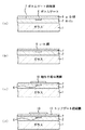
続いて、ボトムゲート電極6と後述するトップゲート電極とを結線するため、トップゲート絶縁膜11の一部分(不図示)で上述のボトムゲート絶縁膜7の一部分と同一部位をエッチング除去した後、図3(a)に示すように、トップゲート絶縁膜11上にボトムゲート電極6と同一の金属材料、即ちここではMo膜12を、露光光(ここではg線)が通過する程度の薄い膜厚、例えば50nm程度に堆積形成する。このとき、上述したボトムゲート絶縁膜7及びトップゲート絶縁膜11の一部を除去した前記一部分を介してボトムゲート電極6とMo膜12とが接続される。
【0030】
続いて、図3(b)に示すように、Mo膜12上に例えばポジ型のフォトレジストを塗布し、ガラス基板1側から、ボトムゲート電極6をマスクとして背面露光する。露光光はボトムゲート電極6では遮断されるがMo膜12は通過するため、ボトムゲート電極6に位置整合してこれと同一形状のレジストパターン13が形成される。
【0031】
そして、図3(c)に示すように、このレジストパターン13をマスクとしてMo膜12をエッチングし、レジストパターン13の形状に倣ったトップゲート電極14を自己整合的に形成する。
【0032】
続いて、レジストパターン13を灰化処理等により除去した後、図3(d)に示すように、トップゲート電極14をマスクとしてトップゲート絶縁膜11をエッチングする。次に、トップゲート電極14をマスクとして動作半導体薄膜10に不純物として例えばリンをイオンドープする。次に、これにエキシマレーザ照射することによりリンを活性化し、ソース/ドレイン15を形成する。なお、不純物の活性化としてはエキシマレーザ活性化に限定したものではなく、熱活性化、ランプ加熱活性化を用いても良い。
【0033】
しかる後、全面を覆うように膜厚300nm程度にSiNを堆積して層間絶縁膜(不図示)を形成した後、コンタクトホールの形成、コンタクトホールを介してソース/ドレイン等と接続する金属電極(不図示)の形成等を経て、TFTを完成させる。
【0034】
なお、TFTを作製する全工程を通じて、熱処理温度を600℃以下とすることが好ましい。これは、600℃より高温ではガラス基板1が変形してしまうからである。
【0035】
以上説明したように、本実施形態によれば、高いgm(高いオン電流)を発揮し、比較的簡素な構成でSi−MOSFETに匹敵する特性を有するTFTを実現することができる。
【0036】
(実施形態2)
図6〜図8は、実施形態2によるTFTの製造方法を工程順に示す模式図であり、図6(a)〜(d),図7(c),図8(a)〜(d)が概略断面図、図8(a),(b),(d)が概略平面図である。
先ず、図6(a)に示すように、ガラス基板21上にバッファ層となるシリコン酸化膜22を膜厚400nm程度に形成した後、シリコン酸化膜22上に金属材料、ここではMo膜を、露光光(ここではg線)が遮断される程度の厚い膜厚、例えば200nm程度に堆積形成し、これを電極形状にパターニングすることにより、ボトムゲート電極23を形成する。
【0037】
続いて、図6(b)に示すように、PECVD法によりボトムゲート電極23を覆うようにシリコン酸化膜24を膜厚60nm程度に形成する。
【0038】
続いて、図6(c)に示すように、シリコン酸化膜24上にアモルファスシリコン(a−Si)膜25を膜厚60nm程度に形成する。
【0039】
続いて、図6(d),7(a)に示すように、a−Si膜25を熱処理して水素出しを行った後、CWレーザを利用して、時間に対して連続したエネルギービームをa−Si膜25に対して照射スキャンする。
【0040】
具体的には、図7(b),(c)に示すように、a−Si膜25は、ボトムゲート電極23上の部位がボトムゲート電極23の形状を反映して凸部25aを形成しており、図4と同様、この凸部25a上でフローパターン結晶が形成される。即ち、凸部25aのテラスでは、段差部分に蓄積されたメルトの固化によって形成された結晶粒が核として作用するために、テラス上で幅が広いフローパターン結晶粒が形成される。これにより、大粒径のポリシリコン結晶を有する多結晶シリコン(p−Si)膜26が形成される。
【0041】
続いて、図7(d)に示すように、p−Si膜26をパターニングし、島状の動作半導体薄膜27を形成する。次に、ボトムゲート電極23と後述するトップゲート電極とを結線するため、ボトムゲート電極23上に形成されたシリコン酸化膜24の一部分(不図示)をエッチング除去する。
【0042】
続いて、図8(a)に示すように、シリコン酸化膜を膜厚60nm程度に形成し、ゲート絶縁膜28を形成した後、ボトムゲート電極23と後述するトップゲート電極とを結線するため、ゲート絶縁膜28の一部分(不図示)で上述のシリコン酸化膜24の一部分と同一部位をエッチング除去した後、ゲート絶縁膜28上にボトムゲート電極23と同一の金属材料、即ちここではMo膜29を、露光光(ここではg線)が通過する程度の薄い膜厚、例えば50nm程度に堆積形成する。このとき、上述したシリコン酸化膜24及びゲート絶縁膜28の一部を除去した前記一部分を介してボトムゲート電極23とMo膜29とが接続される。
【0043】
続いて、図8(b)に示すように、Mo膜29上に例えばポジ型のフォトレジストを塗布し、ガラス基板21側から、ボトムゲート電極23をマスクとして背面露光する。露光光はボトムゲート電極23では遮断されるがMo膜29は通過するため、ボトムゲート電極23に位置整合してこれと同一形状のレジストパターン30が形成される。
【0044】
そして、図8(c)に示すように、このレジストパターン30をマスクとしてMo膜39をエッチングし、レジストパターン30の形状に倣ったトップゲート電極31を自己整合的に形成する。
【0045】
続いて、レジストパターン30を灰化処理等により除去した後、図8(d)に示すように、トップゲート電極31をマスクとしてゲート絶縁膜28をエッチングする。次に、トップゲート電極31をマスクとして動作半導体薄膜27に不純物として例えばリンをイオンドープする。次に、これにエキシマレーザ照射することによりリンを活性化し、トップゲート電極31の両側にソース/ドレイン32を形成する。なお、不純物の活性化としてはエキシマレーザ活性化に限定したものではなく、熱活性化、ランプ加熱活性化を用いても良い。
【0046】
しかる後、全面を覆うように膜厚300nm程度にSiNを堆積して層間絶縁膜(不図示)を形成した後、コンタクトホールの形成、コンタクトホールを介してソース/ドレイン等と接続する金属電極(不図示)の形成等を経て、TFTを完成させる。
【0047】
以上説明したように、本実施形態によれば、高いgm(高いオン電流)を発揮し、比較的簡素な構成でSi−MOSFETに匹敵する特性を有するTFTを実現することができる。
【0048】
(実施形態3)
図9〜図11は、実施形態3によるTFTの製造方法を工程順に示す概略断面図である。なお便宜上、第1の実施形態と対応する構成部材等については同符号を付す。
【0049】
先ず、図9(a)に示すように、ガラス基板1上にバッファ層となるシリコン酸化膜2を膜厚400nm程度に形成した後、例えばネガ型のフォトレジストを塗布し、フォトリソグラフィーによりトップゲート電極形状の溝パターン3aを有するレジストパターン3を形成する。
【0050】
続いて、図9(b)に示すように、レジストパターン3をマスクとしてシリコン酸化膜2の表層をRIEによりエッチングし、シリコン酸化膜2に溝パターン3aに倣った溝4を深さ100nm程度に形成する。
【0051】
続いて、図9(c)に示すように、例えばスパッタ法により、溝4を埋め込むようにシリコン酸化膜2上に金属材料、ここではMo膜5を、露光光(ここではg線)が遮断される程度の厚い膜厚、例えば300nm程度に堆積形成する。
【0052】
続いて、図9(d)に示すように、例えば化学機械研磨法(Chemical Mechanical Polishing:CMP)によりシリコン酸化膜2をストッパーとしてMo膜5を研磨して溝4内のみにMo膜5を残し、ボトムゲート電極6を形成する。
【0053】
続いて、図10(a)に示すように、ボトムゲート電極6上に例えばPECVD法によりシリコン酸化膜を膜厚60nm程度に形成し、ボトムゲート絶縁膜7を形成した後、ボトムゲート絶縁膜7上にアモルファスシリコン(a−Si)膜8を膜厚60nm程度に形成する。
【0054】
続いて、図10(b)に示すように、a−Si膜8を熱処理して水素出しを行った後、CWレーザを利用して、時間に対して連続したエネルギービームをa−Si膜8に対して照射スキャンすることにより、大粒径のポリシリコン結晶を有する多結晶シリコン(p−Si)膜9を形成する。具体的には、図4に示すように、結晶粒の大きい流線形状であるフローパターンの結晶状態に形成され、この結晶粒は、その結晶粒界が手前に存在する他の前記結晶粒から発生するとともに後方において他の結晶粒界と合体しており、且つ結晶粒界がレーザスキャン方向Mに略平行に走る形状とされ、後述するソース・ドレイン間を結ぶ方向が結晶粒の長軸と略平行となる。このときの結晶粒径は数μm程度となり、非常に大きな結晶を形成できる。この結晶粒径は現在使用されているエキシマレーザの10倍〜100倍の大きさになる。
【0055】
続いて、図10(c)及び図5に示すように、p−Si膜9をパターニングし、島状の動作半導体薄膜10を形成する。次に、ボトムゲート電極6と後述するトップゲート電極とを結線するため、ボトムゲート電極6上に形成されたボトムゲート絶縁膜7の一部分(不図示)をエッチング除去する。
【0056】
続いて、図10(d)に示すように、動作半導体薄膜10を覆うように、ボトムゲート絶縁膜7上に例えばPECVD法によりシリコン酸化膜を膜厚60nm程度に形成し、トップゲート絶縁膜11を形成する。このように、ボトムゲート絶縁膜とトップゲート絶縁膜とを同一の絶縁材料で形成することが好ましい。
【0057】
続いて、ボトムゲート電極6と後述するトップゲート電極とを結線するため、トップゲート絶縁膜11の一部分(不図示)で上述のボトムゲート絶縁膜7の一部分と同一部位をエッチング除去する。
【0058】
続いて、金属層及び当該金属層よりも光透過率の高い高透過率材層とが積層されてなる多層構造のトップゲート電極を形成する。
具体的には、先ず図11(a)に示すように、トップゲート絶縁膜11上にボトムゲート電極6と同一の金属材料、即ちここではMo膜41を、露光光(ここではg線)が通過する程度の薄い膜厚、例えば50nm程度に堆積形成する。このとき、上述したボトムゲート絶縁膜7及びトップゲート絶縁膜11の一部を除去した前記一部分を介してボトムゲート電極6とMo膜41とが接続される。更に、Mo膜41上に高透過率材料、ここでは例えば露光光に対して透明な導電膜であるITO膜42を膜厚200nm程度に堆積形成する。
【0059】
続いて、図3(b)に示すように、ITO膜42上に例えばポジ型のフォトレジストを塗布し、ガラス基板1側から、ボトムゲート電極6をマスクとして背面露光する。露光光はボトムゲート電極6では遮断されるがMo膜41及びITO膜42は通過するため、ボトムゲート電極6に位置整合してこれと同一形状のレジストパターン13が形成される。
【0060】
そして、図3(c)に示すように、このレジストパターン13をマスクとしてMo膜41及びITO膜42をエッチングし、レジストパターン13の形状に倣った2層構造のトップゲート電極43を自己整合的に形成する。
【0061】
続いて、レジストパターン13を灰化処理等により除去した後、図3(d)に示すように、トップゲート電極43(Mo膜41及びITO膜42)をマスクとしてトップゲート絶縁膜11をエッチングする。次に、トップゲート電極43をマスクとして動作半導体薄膜10に不純物として例えばリンをイオンドープする。次に、これにエキシマレーザ照射することによりリンを活性化し、ソース/ドレイン15を形成する。なお、不純物の活性化としてはエキシマレーザ活性化に限定したものではなく、熱活性化、ランプ加熱活性化を用いても良い。
【0062】
しかる後、全面を覆うように膜厚300nm程度にSiNを堆積して層間絶縁膜(不図示)を形成した後、コンタクトホールの形成、コンタクトホールを介してソース/ドレイン等と接続する金属電極(不図示)の形成等を経て、TFTを完成させる。
【0063】
なお、TFTを作製する全工程を通じて、熱処理温度を600℃以下とすることが好ましい。これは、600℃より高温ではガラス基板1が変形してしまうからである。
【0064】
以上説明したように、本実施形態によれば、高いgm(高いオン電流)を発揮し、比較的簡素な構成でSi−MOSFETに匹敵する特性を有するTFTを実現することができる。
【0065】
(実施形態4)
図12〜図14は、実施形態4によるTFTの製造方法を工程順に示す模式図であり、図12(a)〜(d),図13(c),図14(a)〜(d)が概略断面図、図13(a),(b),(d)が概略平面図である。なお便宜上、第2の実施形態と対応する構成部材等については同符号を付す。
【0066】
先ず、図12(a)に示すように、ガラス基板21上にバッファ層となるシリコン酸化膜22を膜厚400nm程度に形成した後、シリコン酸化膜22上に金属材料、ここではMo膜を、露光光(ここではg線)が遮断される程度の厚い膜厚、例えば200nm程度に堆積形成し、これを電極形状にパターニングすることにより、ボトムゲート電極23を形成する。
【0067】
続いて、図12(b)に示すように、PECVD法によりボトムゲート電極23を覆うようにシリコン酸化膜24を膜厚60nm程度に形成する。
【0068】
続いて、図12(c)に示すように、シリコン酸化膜24上にアモルファスシリコン(a−Si)膜25を膜厚60nm程度に形成する。
【0069】
続いて、図12(d),13(a)に示すように、a−Si膜25を熱処理して水素出しを行った後、CWレーザを利用して、時間に対して連続したエネルギービームをa−Si膜25に対して照射スキャンする。
【0070】
具体的には、図13(b),(c)に示すように、a−Si膜25は、ボトムゲート電極23上の部位がボトムゲート電極23の形状を反映して凸部25aを形成しており、図4と同様、この凸部25a上でフローパターン結晶が形成される。即ち、凸部25aのテラスでは、段差部分に蓄積されたメルトの固化によって形成された結晶粒が核として作用するために、テラス上で幅が広いフローパターン結晶粒が形成される。これにより、大粒径のポリシリコン結晶を有する多結晶シリコン(p−Si)膜26が形成される。
【0071】
続いて、図13(d)に示すように、p−Si膜26をパターニングし、島状の動作半導体薄膜27を形成する。次に、ボトムゲート電極23と後述するトップゲート電極とを結線するため、ボトムゲート電極23上に形成されたシリコン酸化膜24の一部分(不図示)をエッチング除去する。
【0072】
続いて、図14(a)に示すように、シリコン酸化膜を膜厚60nm程度に形成し、ゲート絶縁膜28を形成した後、ボトムゲート電極23と後述するトップゲート電極とを結線するため、ゲート絶縁膜28の一部分(不図示)で上述のシリコン酸化膜24の一部分と同一部位をエッチング除去する。
【0073】
続いて、金属層及び当該金属層よりも光透過率の高い高透過率材層とが積層されてなる多層構造のトップゲート電極を形成する。
具体的には、先ずゲート絶縁膜28上にボトムゲート電極23と同一の金属材料、即ちここではMo膜44を、露光光(ここではg線)が通過する程度の薄い膜厚、例えば50nm程度に堆積形成する。このとき、上述したシリコン酸化膜24及びゲート絶縁膜28の一部を除去した前記一部分を介してボトムゲート電極23とMo膜44とが接続される。更に、Mo膜44上に高透過率材料、ここでは例えば露光光に対して透明な導電膜であるITO膜45を膜厚200nm程度に堆積形成する。
【0074】
続いて、図14(b)に示すように、ITO膜45上に例えばポジ型のフォトレジストを塗布し、ガラス基板21側から、ボトムゲート電極23をマスクとして背面露光する。露光光はボトムゲート電極23では遮断されるがMo膜44及びITO膜45は通過するため、ボトムゲート電極23に位置整合してこれと同一形状のレジストパターン30が形成される。
【0075】
そして、図14(c)に示すように、このレジストパターン30をマスクとしてMo膜44及びITO膜45をエッチングし、レジストパターン30の形状に倣った2層構造のトップゲート電極46を自己整合的に形成する。
【0076】
続いて、レジストパターン30を灰化処理等により除去した後、図14(d)に示すように、トップゲート電極46(Mo膜44及びITO膜45)をマスクとしてゲート絶縁膜28をエッチングする。次に、トップゲート電極46をマスクとして動作半導体薄膜27に不純物として例えばリンをイオンドープする。次に、これにエキシマレーザ照射することによりリンを活性化し、トップゲート電極46の両側にソース/ドレイン32を形成する。なお、不純物の活性化としてはエキシマレーザ活性化に限定したものではなく、熱活性化、ランプ加熱活性化を用いても良い。
【0077】
しかる後、全面を覆うように膜厚300nm程度にSiNを堆積して層間絶縁膜(不図示)を形成した後、コンタクトホールの形成、コンタクトホールを介してソース/ドレイン等と接続する金属電極(不図示)の形成等を経て、TFTを完成させる。
【0078】
上記方法により、実際に作製されたTFTの顕微鏡写真を図15に、このTFTの特性を図16にそれぞれ示す。図16では、横軸がゲート電圧(VG(V))を示し、左側の縦軸がドレイン電流(ID(A))を、右側の縦軸が移動度(cm2/Vs:トップゲートTFTと仮定し、gmから求めた移動度)をそれぞれ示す。このTFTにおいては、800cm2/Vsという極めて高い移動度が得られ、またS値は100mV/decと小値を示しており、優れたTFTを有することが判った。
【0079】
以上説明したように、本実施形態によれば、高いgm(高いオン電流)を発揮し、比較的簡素な構成でSi−MOSFETに匹敵する特性を有するTFTを実現することができる。
【0080】
以下、本発明の諸態様を付記としてまとめて記載する。
【0081】
(付記1)非晶質透明基板と、
前記非晶質透明基板上に形成された動作半導体薄膜と、
前記非晶質透明基板上において、前記動作半導体薄膜の上下にそれぞれ絶縁膜を介して同一の金属材料から形成されてなる上部ゲート電極及び下部ゲート電極と
を含み、
前記上部ゲート電極と前記下部ゲート電極とは相異なる膜厚に形成されていることを特徴とする半導体装置。
【0082】
(付記2)前記上部ゲート電極は、前記下部ゲート電極よりも薄い膜厚に形成されていることを特徴とする付記1に記載の半導体装置。
【0083】
(付記3)非晶質透明基板と、
前記非晶質透明基板上に形成された動作半導体薄膜と、
前記非晶質透明基板上において、前記動作半導体薄膜の上下にそれぞれ絶縁膜を介して形成された上部ゲート電極及び下部ゲート電極と
を含み、
前記上部ゲート電極は、金属層と当該金属層よりも光透過率の高い高透過率材料層とが積層されてなり、
前記上部ゲート電極の前記金属層と前記下部ゲート電極とは、同一の金属材料からなるとともに、相異なる膜厚に形成されてなることを特徴とする半導体装置。
【0084】
(付記4)前記上部ゲート電極の前記高透過率材料層は、透明導電材料からなることを特徴とする付記3に記載の半導体装置。
【0085】
(付記5)前記上部ゲート電極の前記金属層は、前記下部ゲート電極よりも薄い膜厚に形成されていることを特徴とする付記1〜4のいずれか1項に記載の半導体装置。
【0086】
(付記6)前記上部ゲート電極と前記下部ゲート電極とは、略同一のゲート長で互いに位置整合して形成されていることを特徴とする付記5に記載の半導体装置。
【0087】
(付記7)前記下部ゲート電極が絶縁材料内に埋め込まれてなり、前記動作半導体薄膜が平坦に形成されていることを特徴とする付記1〜6のいずれか1項に記載の半導体装置。
【0088】
(付記8)前記動作半導体薄膜は、そのソース/ドレインの部分がチャネルの部分よりも低い位置に形成されてなることを特徴とする付記1〜6いずれか1項に記載の半導体装置。
【0089】
(付記9)前記動作半導体薄膜が多結晶シリコンから形成されていることを特徴とする付記1〜8のいずれか1項に記載の半導体装置。
【0090】
(付記10)前記動作半導体膜は、結晶粒の大きい流線形状であるフローパターンの結晶状態に形成されており、
前記結晶粒は、その結晶粒界が手前に存在する他の前記結晶粒から発生するとともに後方において他の結晶粒界と合体しており、且つ結晶粒界がレーザスキャン方向に略平行に走る形状とされていることを特徴とする付記9に記載の半導体装置。
【0091】
(付記11)前記動作半導体膜は、膜厚が100nm以下に形成されていることを特徴とする付記1〜10のいずれか1項に記載の半導体装置。
【0092】
(付記12)非晶質透明基板上に金属材料を堆積し、前記金属材料を加工して下部ゲート電極を形成する工程と、
前記下部ゲート電極上に絶縁膜を介して半導体膜を堆積し、前記半導体膜を加工して動作半導体膜を形成する工程と、
前記動作半導体膜上に絶縁膜を介して前記下部ゲート電極よりも薄く、同一の前記金属材料を堆積し、前記下部ゲート電極をマスクとして前記非晶質透明基板の背面から露光することにより前記金属材料を加工し、前記下部ゲート電極に整合した上部ゲート電極を形成する工程と
を含むことを特徴とする半導体装置の製造方法。
【0093】
(付記13)非晶質透明基板上に金属材料を堆積し、前記金属材料を加工して下部ゲート電極を形成する工程と、
前記下部ゲート電極上に絶縁膜を介して半導体膜を堆積し、前記半導体膜を加工して動作半導体膜を形成する工程と、
前記動作半導体膜上に絶縁膜を介して、前記下部ゲート電極よりも薄い同一の前記金属材料と、当該金属材料よりも光透過率の高い高透過率材料とを順次堆積し、前記下部ゲート電極をマスクとして前記非晶質透明基板の背面から露光することにより前記金属材料及び前記高透過率材料を加工し、前記下部ゲート電極に整合した上部ゲート電極を形成する工程と
を含むことを特徴とする半導体装置の製造方法。
【0094】
(付記14)前記上部ゲート電極の前記高透過率材料層は、透明導電材料からなることを特徴とする付記13に記載の半導体装置の製造方法。
【0095】
(付記15)アモルファス状態の前記半導体膜に時間に対して連続的にエネルギーを出力するエネルギービームを照射し、前記半導体膜を結晶化することを特徴とする付記12〜14のいずれか1項に記載の半導体装置の製造方法。
【0096】
(付記16)前記エネルギービームの出力不安定性が±1%より小値であることを特徴とする付記15に記載の半導体装置の製造方法。
【0097】
(付記17)前記エネルギービームの時間に対する不安定性を示すノイズが0.1rms%以下である付記15又は16に記載の半導体装置の製造方法。
【0098】
(付記18)前記エネルギービームは、半導体励起の固体レーザによるものであることを特徴とする付記15〜17のいずれか1項に記載の半導体装置の製造方法。
【0099】
(付記19)前記下部ゲート電極を絶縁材料内に埋め込み形成し、前記動作半導体薄膜を平坦に形成することを特徴とする付記12〜18のいずれか1項に記載の半導体装置の製造方法。
【0100】
(付記20)化学機械研磨法により前記下部ゲート電極を埋め込み形成することを特徴とする付記19に記載の半導体装置の製造方法。
【0101】
(付記21)前記動作半導体薄膜は、前記下部ゲート電極の形状を反映して、そのソース/ドレインの部分がチャネルの部分よりも低い位置に形成されることを特徴とする付記12〜18のいずれか1項に記載の半導体装置の製造方法。
【0102】
(付記22)各製造工程における処理温度が600℃以下であることを特徴とする付記12〜21のいずれか1項に記載の半導体装置の製造方法。
【0103】
【発明の効果】
本発明によれば、透明非晶質基板上に、高い移動度を実現できる半導体薄膜とメタルゲートを有するダブルゲート構造を組み合わせることにより、Si−MOSFETに匹敵する特性を有するTFTを実現することが可能となる。
【図面の簡単な説明】
【図1】本発明の実施形態1によるTFTの製造方法を工程順に示す概略断面図である。
【図2】図1に引き続き、本発明の実施形態1によるTFTの製造方法を工程順に示す概略断面図である。
【図3】図2に引き続き、本発明の実施形態1によるTFTの製造方法を工程順に示す概略断面図である。
【図4】CWレーザの照射スキャンにより結晶化されてなるフローパターンの様子を示す顕微鏡写真である。
【図5】アイランド形状にパターニングされた動作半導体薄膜を示す概略平面図である。
【図6】本発明の実施形態2によるTFTの製造方法を工程順に示す概略断面図である。
【図7】図6に引き続き、本発明の実施形態2によるTFTの製造方法を工程順に示す概略断面図である。
【図8】図7に引き続き、本発明の実施形態2によるTFTの製造方法を工程順に示す概略断面図である。
【図9】本発明の実施形態3によるTFTの製造方法を工程順に示す概略断面図である。
【図10】図9に引き続き、本発明の実施形態3によるTFTの製造方法を工程順に示す概略断面図である。
【図11】図10に引き続き、本発明の実施形態3によるTFTの製造方法を工程順に示す概略断面図である。
【図12】本発明の実施形態4によるTFTの製造方法を工程順に示す概略断面図である。
【図13】図11に引き続き、本発明の実施形態4によるTFTの製造方法を工程順に示す概略断面図である。
【図14】図13に引き続き、本発明の実施形態4によるTFTの製造方法を工程順に示す概略断面図である。
【図15】本発明の手法により実際に作製されたTFTの様子を示す顕微鏡写真である。
【図16】本発明の手法により実際に作製されたTFTの特性を示す特性図である。
【符号の説明】
1,21 ガラス基板
2,22,24 シリコン酸化膜
3,13,30 レジストパターン
3a 溝パターン
4 溝
5,12,29,41,44 Mo膜
6,23 ボトムゲート電極
7 ボトムゲート絶縁膜
8,25 アモルファスシリコン(a−Si)膜
25a 凸部
9,26 多結晶シリコン(p−Si)膜
10,27 動作半導体薄膜
11 トップゲート絶縁膜
14,31,44,46 トップゲート電極
15,32 ソース/ドレイン
28 ゲート絶縁膜
42,45 ITO膜[0001]
TECHNICAL FIELD OF THE INVENTION
The present invention relates to a semiconductor device and a method for manufacturing the same, and more particularly to a thin film transistor (TFT) provided on an amorphous transparent substrate.
[0002]
[Prior art]
Recently, a high-definition display in which a polycrystalline semiconductor TFT (particularly, a polycrystalline silicon TFT (p-SiTFT)) is formed on an alkali-free glass substrate has been realized. As a method of forming a p-Si film serving as an operation semiconductor thin film of a p-Si TFT, first, an amorphous silicon (a-Si) film is formed, and then short-wave excimer laser light with an ultraviolet wavelength is irradiated. Accordingly, a method of obtaining a p-Si film by melting and crystallizing only an a-Si film without affecting a glass substrate has become mainstream.
[0003]
[Patent Document 1]
U.S. Patent Application Publication No. 2002 / 0031876A1
[Patent Document 2]
JP-A-10-173192
[Patent Document 3]
JP-A-2002-33481
[Non-patent document 1]
2001 AM-LCD p. 243
[0004]
[Problems to be solved by the invention]
In forming the p-Si film by the above method, a high-output, linear-beam excimer laser corresponding to a large area is used, and a top gate type excimer laser using a crystallized p-Si film is used. Thin film transistors have been developed. Excimer laser crystallization isotropically grows from randomly generated nuclei, the crystal grain size is less than 1 μm, and the channel region contains a large number of crystal grains due to the small crystal grain size. Mobility typically 150 cm 2 / Vs. This value is about 100 times higher in mobility than a-Si, but is about 1/4 compared to the mobility of single crystal silicon (Si-MOSFET). The mobility is large when the crystal grain size is large and the number of grain boundaries existing in the channel length direction is small, and when the crystal grain size of the channel portion is small and there are many grain boundaries in the channel length direction. Becomes smaller. Further, the crystal grain boundaries have many defects, and the characteristics are suppressed by the presence of the grain boundaries inside the channel. Therefore, in order to realize a high gm with a polycrystalline semiconductor thin film, it is necessary to increase the crystal grain size or to adopt some TFT structure capable of realizing a high gm (high on-current).
[0005]
The present invention has been made in view of the above problems, and provides a TFT which exhibits a high gm (high on-current), has a relatively simple configuration, and has characteristics comparable to a Si-MOSFET, and a method for manufacturing the same. With the goal.
[0006]
[Means for Solving the Problems]
As a result of intensive studies, the present inventor has reached various aspects of the invention described below.
[0007]
The semiconductor device of the present invention includes an amorphous transparent substrate, an operating semiconductor thin film formed on the amorphous transparent substrate, and an insulating film on the amorphous transparent substrate, above and below the operating semiconductor thin film. An upper gate electrode and a lower gate electrode are formed of the same metal material with the upper and lower gate electrodes interposed therebetween, and the upper gate electrode and the lower gate electrode are formed to have different thicknesses.
[0008]
The semiconductor device of the present invention includes an amorphous transparent substrate, an operating semiconductor thin film formed on the amorphous transparent substrate, and an insulating film on the amorphous transparent substrate, above and below the operating semiconductor thin film. An upper gate electrode and a lower gate electrode formed through the upper gate electrode, wherein the upper gate electrode is formed by laminating a metal layer and a high transmittance material layer having a higher light transmittance than the metal layer. The metal layer of the electrode and the lower gate electrode are made of the same metal material and have different thicknesses.
[0009]
A method for manufacturing a semiconductor device according to the present invention includes the steps of: depositing a metal material on an amorphous transparent substrate; processing the metal material to form a lower gate electrode; and forming an insulating film on the lower gate electrode via an insulating film. Depositing a semiconductor film, processing the semiconductor film to form an active semiconductor film, and depositing the same metal material thinner than the lower gate electrode via an insulating film on the active semiconductor film, Processing the metal material by exposing from the back surface of the amorphous transparent substrate using the lower gate electrode as a mask to form an upper gate electrode aligned with the lower gate electrode.
[0010]
A method for manufacturing a semiconductor device according to the present invention includes the steps of: depositing a metal material on an amorphous transparent substrate; processing the metal material to form a lower gate electrode; and forming an insulating film on the lower gate electrode via an insulating film. Depositing a semiconductor film, processing the semiconductor film to form an active semiconductor film, and an insulating film on the active semiconductor film, the same metal material thinner than the lower gate electrode; The metal material and the high transmittance material are processed by sequentially depositing a high transmittance material having a higher light transmittance than the material, and exposing from the back surface of the amorphous transparent substrate using the lower gate electrode as a mask. Forming an upper gate electrode aligned with the lower gate electrode.
[0011]
BEST MODE FOR CARRYING OUT THE INVENTION
-Basic gist of the present invention-
In order to realize a TFT having a high mobility comparable to that of a Si-MOSFET, the present inventor uses a polycrystalline semiconductor thin film as an operating semiconductor thin film, and connects each gate electrode above and below the operating semiconductor thin film via a gate insulating film. I came up with the idea of adopting a double gate structure.
[0012]
Since it is extremely difficult to align the upper and lower gate electrodes in the double gate structure, it cannot be realized by a Si-MOSFET using a Si substrate. In order to realize a TFT having such a structure, the use of a TFT using a transparent amorphous substrate such as glass is utilized. That is, the upper gate electrode (top gate electrode) may be formed in a self-aligned manner by back exposure from the substrate side using the lower gate electrode (bottom gate electrode) as a mask.
[0013]
Utilizing such a technique, a TFT is actually manufactured by Asano et al. (See Non-Patent Document 1). In their experiments, they used low-resistance polycrystalline silicon gates. In order to form a low-resistance polycrystalline silicon film, it is necessary to perform a heat treatment at a high temperature, so that it cannot be applied to glass. They use quartz glass.
[0014]
Further, a technique is disclosed in which the top gate electrode is formed in a self-aligned manner using the bottom gate electrode as a mask by changing the material of the bottom gate electrode and the material of the top gate electrode (see Patent Document 2).
[0015]
However, in this case, it is necessary that the exposure light pass through the substrate and be blocked at the portion of the bottom gate electrode, and at the portion where the bottom gate electrode does not exist, the exposure light passes through the conductive film serving as the top gate electrode. In order to satisfy such conditions, each gate electrode is formed of a metal material, and the bottom gate electrode is formed to a thickness small enough to allow the exposure light to pass through the metal film serving as the top gate electrode. May be formed to have a large thickness. Here, by forming the bottom gate electrode and the top gate electrode with the same metal material, the connection between them can be easily and reliably secured, the threshold voltage can be easily controlled, and the characteristics can be improved. . This makes it possible to obtain gm (mobility) about twice that of a normal single-gate TFT. By forming each of the gate electrodes with a metal material, it is easy to connect them at a predetermined position.
[0016]
In this case, in order to efficiently and accurately perform the above-described back exposure, it is preferable that the conductive film serving as the top gate electrode be formed as thin as possible. On the other hand, there is an inconvenience that the resistance value of the top gate electrode is increased as the thickness is reduced. The present inventor has requested that the top gate electrode be formed of the same metal material as the bottom gate electrode, in order to sufficiently satisfy both of the requests for the back exposure and the reduction of the resistance value without sacrificing one of them. The present inventors have conceived of forming a laminated structure with a high transmittance material layer having higher light transmittance than the metal layer. That is, the requirement for back exposure is satisfied by a metal layer that is thinner (as much as possible) than the bottom gate electrode, and the requirement for reduction in resistance is satisfied by a high transmittance material layer represented by a transparent conductive material.
[0017]
Further, when crystallizing and forming a polycrystalline semiconductor thin film serving as an operating semiconductor thin film, a large grain polysilicon can be formed by scanning and scanning a continuous energy beam with respect to time. The crystal grain size at this time is about several microns, and has a very large grain size. The crystal grain size is 10 to 100 times larger than the currently used excimer laser, and the mobility is about 2 to 3 times that of the excimer laser. 2 / Vs ~ 400cm 2 / Vs.
[0018]
Therefore, a TFT having characteristics comparable to those of a Si-MOSFET can be formed by combining an operating semiconductor thin film capable of realizing high mobility with a double gate structure. The present invention is most suitable for circuits formed on an amorphous transparent substrate and requiring high-speed operation.
[0019]
-Specific embodiments to which the present invention is applied-
Hereinafter, specific embodiments of the present invention will be described in detail.
Here, crystallization using a semiconductor-pumped (LD-pumped) solid-state laser (DPSS laser) as a CW (Continuous Wave) laser is exemplified. The laser wavelength is 532 nm and the output is 10 W. Energy beam output stability is noise of 0.1 rms% or less, and output time stability is ± 1% / hour or less. Note that the laser wavelength is not limited to this value, and a wavelength at which the amorphous semiconductor film can be crystallized may be used.
[0020]
Although NA35 glass is used for the amorphous transparent substrate, the substrate material is not limited to this, and other non-alkali glass, quartz glass, plastic, or the like may be used.
[0021]
(Embodiment 1)
1 to 3 are schematic cross-sectional views showing a method for manufacturing a TFT according to the first embodiment in the order of steps.
First, as shown in FIG. 1A, after a
[0022]
Subsequently, as shown in FIG. 1B, the surface layer of the
[0023]
Subsequently, as shown in FIG. 1 (c), a metal material, here a
[0024]
Subsequently, as shown in FIG. 1D, the
[0025]
Subsequently, as shown in FIG. 2A, a silicon oxide film is formed on the
[0026]
Subsequently, as shown in FIG. 2B, after the
[0027]
Subsequently, as shown in FIGS. 2C and 5, the p-
[0028]
Subsequently, as shown in FIG. 2D, a silicon oxide film is formed to a thickness of about 60 nm by PECVD so as to cover the operating semiconductor
[0029]
Subsequently, in order to connect the
[0030]
Subsequently, as shown in FIG. 3B, for example, a positive-type photoresist is applied on the
[0031]
Then, as shown in FIG. 3C, the
[0032]
Subsequently, after the resist
[0033]
Thereafter, SiN is deposited to a thickness of about 300 nm so as to cover the entire surface to form an interlayer insulating film (not shown), and then a contact hole is formed, and a metal electrode (for connecting to a source / drain via the contact hole) is formed. (Not shown), and the like, to complete the TFT.
[0034]
Note that the heat treatment temperature is preferably set to 600 ° C. or lower throughout all steps of manufacturing the TFT. This is because the
[0035]
As described above, according to the present embodiment, it is possible to realize a TFT exhibiting high gm (high on-state current) and having characteristics comparable to those of a Si-MOSFET with a relatively simple configuration.
[0036]
(Embodiment 2)
6 to 8 are schematic views showing a method of manufacturing a TFT according to the second embodiment in the order of steps. FIGS. 6 (a) to 6 (d), 7 (c), and 8 (a) to 8 (d) FIGS. 8A, 8B, and 8D are schematic plan views.
First, as shown in FIG. 6A, after a
[0037]
Subsequently, as shown in FIG. 6B, a
[0038]
Subsequently, as shown in FIG. 6C, an amorphous silicon (a-Si)
[0039]
Subsequently, as shown in FIGS. 6D and 7A, after the
[0040]
Specifically, as shown in FIGS. 7B and 7C, in the
[0041]
Subsequently, as shown in FIG. 7D, the p-Si film 26 is patterned to form an island-shaped operating semiconductor
[0042]
Subsequently, as shown in FIG. 8A, a silicon oxide film is formed to a thickness of about 60 nm, a
[0043]
Subsequently, as shown in FIG. 8B, for example, a positive photoresist is applied on the
[0044]
Then, as shown in FIG. 8C, the Mo film 39 is etched using the resist pattern 30 as a mask to form a
[0045]
Subsequently, after the resist pattern 30 is removed by an ashing process or the like, as shown in FIG. 8D, the
[0046]
Thereafter, SiN is deposited to a thickness of about 300 nm so as to cover the entire surface to form an interlayer insulating film (not shown), and then a contact hole is formed, and a metal electrode (for connecting to a source / drain via the contact hole) is formed. (Not shown), and the like, to complete the TFT.
[0047]
As described above, according to the present embodiment, it is possible to realize a TFT exhibiting high gm (high on-state current) and having characteristics comparable to those of a Si-MOSFET with a relatively simple configuration.
[0048]
(Embodiment 3)
9 to 11 are schematic cross-sectional views illustrating a method of manufacturing a TFT according to the third embodiment in the order of steps. For the sake of convenience, the same reference numerals are given to components and the like corresponding to the first embodiment.
[0049]
First, as shown in FIG. 9A, a
[0050]
Subsequently, as shown in FIG. 9B, the surface layer of the
[0051]
Subsequently, as shown in FIG. 9C, a metal material, here a
[0052]
Subsequently, as shown in FIG. 9D, the
[0053]
Subsequently, as shown in FIG. 10A, a silicon oxide film is formed on the
[0054]
Subsequently, as shown in FIG. 10B, after the
[0055]
Subsequently, as shown in FIGS. 10C and 5, the p-
[0056]
Subsequently, as shown in FIG. 10D, a silicon oxide film is formed to a thickness of about 60 nm on the bottom
[0057]
Subsequently, in order to connect the
[0058]
Subsequently, a top gate electrode having a multilayer structure in which a metal layer and a high transmittance material layer having higher light transmittance than the metal layer is stacked is formed.
Specifically, first, as shown in FIG. 11A, the same metal material as the
[0059]
Subsequently, as shown in FIG. 3B, for example, a positive photoresist is applied on the
[0060]
Then, as shown in FIG. 3C, the
[0061]
Subsequently, after the resist
[0062]
Thereafter, SiN is deposited to a thickness of about 300 nm so as to cover the entire surface to form an interlayer insulating film (not shown), and then a contact hole is formed, and a metal electrode (for connecting to a source / drain via the contact hole) is formed. (Not shown), and the like, to complete the TFT.
[0063]
Note that the heat treatment temperature is preferably set to 600 ° C. or lower throughout all steps of manufacturing the TFT. This is because the
[0064]
As described above, according to the present embodiment, it is possible to realize a TFT exhibiting high gm (high on-state current) and having characteristics comparable to those of a Si-MOSFET with a relatively simple configuration.
[0065]
(Embodiment 4)
12 to 14 are schematic diagrams showing a method of manufacturing a TFT according to the fourth embodiment in the order of steps. FIGS. 12 (a) to 12 (d), 13 (c), and 14 (a) to 14 (d) 13 (a), 13 (b) and 13 (d) are schematic plan views. For the sake of convenience, the same reference numerals are given to components and the like corresponding to the second embodiment.
[0066]
First, as shown in FIG. 12A, after a
[0067]
Subsequently, as shown in FIG. 12B, a
[0068]
Subsequently, as shown in FIG. 12C, an amorphous silicon (a-Si)
[0069]
Subsequently, as shown in FIGS. 12D and 13A, after the heat treatment of the
[0070]
Specifically, as shown in FIGS. 13B and 13C, in the
[0071]
Subsequently, as shown in FIG. 13D, the p-Si film 26 is patterned to form an island-shaped operating semiconductor
[0072]
Subsequently, as shown in FIG. 14A, a silicon oxide film is formed to a thickness of about 60 nm, a
[0073]
Subsequently, a top gate electrode having a multilayer structure in which a metal layer and a high transmittance material layer having higher light transmittance than the metal layer is stacked is formed.
Specifically, first, the same metal material as the
[0074]
Subsequently, as shown in FIG. 14B, for example, a positive photoresist is applied on the
[0075]
Then, as shown in FIG. 14C, the
[0076]
Subsequently, after the resist pattern 30 is removed by an ashing process or the like, as shown in FIG. 14D, the
[0077]
Thereafter, SiN is deposited to a thickness of about 300 nm so as to cover the entire surface to form an interlayer insulating film (not shown), and then a contact hole is formed, and a metal electrode (for connecting to a source / drain via the contact hole) is formed. (Not shown), and the like, to complete the TFT.
[0078]
FIG. 15 shows a micrograph of a TFT actually manufactured by the above method, and FIG. 16 shows characteristics of the TFT. In FIG. 16, the horizontal axis is the gate voltage (V G (V)), and the vertical axis on the left is the drain current (I D (A)), the vertical axis on the right shows the mobility (cm). 2 / Vs: mobility assuming top gate TFT and calculated from gm). In this TFT, 800 cm 2 / Vs, and an S value as small as 100 mV / dec, indicating an excellent TFT.
[0079]
As described above, according to the present embodiment, it is possible to realize a TFT exhibiting high gm (high on-state current) and having characteristics comparable to those of a Si-MOSFET with a relatively simple configuration.
[0080]
Hereinafter, various aspects of the present invention will be collectively described as supplementary notes.
[0081]
(Supplementary Note 1) Amorphous transparent substrate;
An operating semiconductor thin film formed on the amorphous transparent substrate,
On the amorphous transparent substrate, an upper gate electrode and a lower gate electrode formed of the same metal material above and below the operating semiconductor thin film via an insulating film, respectively.
Including
A semiconductor device, wherein the upper gate electrode and the lower gate electrode are formed to have different thicknesses.
[0082]
(Supplementary Note 2) The semiconductor device according to
[0083]
(Supplementary Note 3) Amorphous transparent substrate,
An operating semiconductor thin film formed on the amorphous transparent substrate,
On the amorphous transparent substrate, an upper gate electrode and a lower gate electrode formed above and below the working semiconductor thin film via an insulating film, respectively.
Including
The upper gate electrode is formed by stacking a metal layer and a high transmittance material layer having a higher light transmittance than the metal layer,
The semiconductor device according to
[0084]
(Supplementary Note 4) The semiconductor device according to supplementary note 3, wherein the high transmittance material layer of the upper gate electrode is made of a transparent conductive material.
[0085]
(Supplementary Note 5) The semiconductor device according to any one of
[0086]
(Supplementary Note 6) The semiconductor device according to
[0087]
(Supplementary note 7) The semiconductor device according to any one of
[0088]
(Supplementary Note 8) The semiconductor device according to any one of
[0089]
(Supplementary note 9) The semiconductor device according to any one of
[0090]
(Supplementary Note 10) The operating semiconductor film is formed in a crystal state of a flow pattern having a streamline shape with large crystal grains,
The crystal grain has a shape in which the crystal grain boundary is generated from another crystal grain present in the front and is united with another crystal grain boundary in the rear, and the crystal grain boundary runs substantially parallel to the laser scanning direction. 10. The semiconductor device according to
[0091]
(Supplementary Note 11) The semiconductor device according to any one of
[0092]
(Supplementary Note 12) a step of depositing a metal material on the amorphous transparent substrate and processing the metal material to form a lower gate electrode;
Depositing a semiconductor film on the lower gate electrode via an insulating film, and processing the semiconductor film to form an active semiconductor film;
By depositing the same metal material thinner than the lower gate electrode via an insulating film on the active semiconductor film and exposing the same from the back surface of the amorphous transparent substrate using the lower gate electrode as a mask, the metal Processing a material to form an upper gate electrode aligned with the lower gate electrode;
A method for manufacturing a semiconductor device, comprising:
[0093]
(Supplementary Note 13) a step of depositing a metal material on the amorphous transparent substrate and processing the metal material to form a lower gate electrode;
Depositing a semiconductor film on the lower gate electrode via an insulating film, and processing the semiconductor film to form an active semiconductor film;
The same metal material thinner than the lower gate electrode and a high transmittance material having a higher light transmittance than the metal material are sequentially deposited on the active semiconductor film via an insulating film, and the lower gate electrode Processing the metal material and the high transmittance material by exposing from the back surface of the amorphous transparent substrate using a mask as a mask to form an upper gate electrode aligned with the lower gate electrode.
A method for manufacturing a semiconductor device, comprising:
[0094]
(Supplementary note 14) The method for manufacturing a semiconductor device according to
[0095]
(Supplementary note 15) The semiconductor device according to any one of
[0096]
(Supplementary note 16) The method of manufacturing a semiconductor device according to
[0097]
(Supplementary note 17) The method of manufacturing a semiconductor device according to
[0098]
(Supplementary note 18) The method of manufacturing a semiconductor device according to any one of
[0099]
(Supplementary note 19) The method of manufacturing a semiconductor device according to any one of
[0100]
(Supplementary note 20) The method for manufacturing a semiconductor device according to supplementary note 19, wherein the lower gate electrode is buried by a chemical mechanical polishing method.
[0101]
(Supplementary note 21) In any one of
[0102]
(Supplementary Note 22) The method of manufacturing a semiconductor device according to any one of
[0103]
【The invention's effect】
According to the present invention, a TFT having characteristics comparable to a Si-MOSFET can be realized by combining a semiconductor thin film capable of realizing high mobility and a double gate structure having a metal gate on a transparent amorphous substrate. It becomes possible.
[Brief description of the drawings]
FIG. 1 is a schematic cross-sectional view showing a method for manufacturing a TFT according to
FIG. 2 is a schematic cross-sectional view showing a manufacturing method of the TFT according to the first embodiment of the present invention in the order of steps, following FIG. 1;
FIG. 3 is a schematic cross-sectional view showing a manufacturing method of the TFT according to the first embodiment of the present invention in the order of steps, following FIG. 2;
FIG. 4 is a micrograph showing a flow pattern that is crystallized by a CW laser irradiation scan.
FIG. 5 is a schematic plan view showing an operating semiconductor thin film patterned in an island shape.
FIG. 6 is a schematic cross-sectional view showing a method for manufacturing a TFT according to
FIG. 7 is a schematic cross-sectional view showing a manufacturing method of the TFT according to the second embodiment of the present invention in the order of steps, following FIG. 6;
FIG. 8 is a schematic cross-sectional view showing a method of manufacturing the TFT according to the second embodiment of the present invention in the order of steps, following FIG. 7;
FIG. 9 is a schematic cross-sectional view showing a method for manufacturing a TFT according to Embodiment 3 of the present invention in the order of steps.
FIG. 10 is a schematic cross-sectional view showing a manufacturing method of the TFT according to the third embodiment of the present invention in the order of steps, following FIG. 9;
FIG. 11 is a schematic cross-sectional view showing a manufacturing method of the TFT according to the third embodiment of the present invention in the order of steps, following FIG. 10;
FIG. 12 is a schematic cross-sectional view showing a method for manufacturing a TFT according to Embodiment 4 of the present invention in the order of steps.
FIG. 13 is a schematic cross-sectional view showing a manufacturing method of the TFT according to the fourth embodiment of the present invention in the order of steps, following FIG. 11;
FIG. 14 is a schematic cross-sectional view showing a method of manufacturing the TFT according to the fourth embodiment of the present invention in the order of steps, following FIG. 13;
FIG. 15 is a micrograph showing a state of a TFT actually manufactured by the method of the present invention.
FIG. 16 is a characteristic diagram showing characteristics of a TFT actually manufactured by the method of the present invention.
[Explanation of symbols]
1,21 glass substrate
2,22,24 silicon oxide film
3,13,30 resist pattern
3a Groove pattern
4 grooves
5,12,29,41,44 Mo film
6,23 Bottom gate electrode
7 Bottom gate insulating film
8,25 Amorphous silicon (a-Si) film
25a convex
9,26 Polycrystalline silicon (p-Si) film
10,27 Working semiconductor thin film
11 Top gate insulating film
14,31,44,46 Top gate electrode
15, 32 source / drain
28 Gate insulating film
42,45 ITO film
Claims (10)
前記非晶質透明基板上に形成された動作半導体薄膜と、
前記非晶質透明基板上において、前記動作半導体薄膜の上下にそれぞれ絶縁膜を介して同一の金属材料から形成されてなる上部ゲート電極及び下部ゲート電極と
を含み、
前記上部ゲート電極と前記下部ゲート電極とは相異なる膜厚に形成されていることを特徴とする半導体装置。An amorphous transparent substrate,
An operating semiconductor thin film formed on the amorphous transparent substrate,
On the amorphous transparent substrate, including an upper gate electrode and a lower gate electrode formed of the same metal material above and below the operating semiconductor thin film via an insulating film, respectively,
A semiconductor device, wherein the upper gate electrode and the lower gate electrode are formed to have different thicknesses.
前記非晶質透明基板上に形成された動作半導体薄膜と、
前記非晶質透明基板上において、前記動作半導体薄膜の上下にそれぞれ絶縁膜を介して形成された上部ゲート電極及び下部ゲート電極と
を含み、
前記上部ゲート電極は、金属層と当該金属層よりも光透過率の高い高透過率材料層とが積層されてなり、
前記上部ゲート電極の前記金属層と前記下部ゲート電極とは、同一の金属材料からなるとともに、相異なる膜厚に形成されてなることを特徴とする半導体装置。An amorphous transparent substrate,
An operating semiconductor thin film formed on the amorphous transparent substrate,
On the amorphous transparent substrate, including an upper gate electrode and a lower gate electrode formed above and below the working semiconductor thin film via an insulating film, respectively.
The upper gate electrode is formed by stacking a metal layer and a high transmittance material layer having a higher light transmittance than the metal layer,
The semiconductor device according to claim 1, wherein the metal layer and the lower gate electrode of the upper gate electrode are made of the same metal material and have different thicknesses.
前記下部ゲート電極上に絶縁膜を介して半導体膜を堆積し、前記半導体膜を加工して動作半導体膜を形成する工程と、
前記動作半導体膜上に絶縁膜を介して前記下部ゲート電極よりも薄く同一の前記金属材料を堆積し、前記下部ゲート電極をマスクとして前記非晶質透明基板の背面から露光することにより前記金属材料を加工し、前記下部ゲート電極に整合した上部ゲート電極を形成する工程と
を含むことを特徴とする半導体装置の製造方法。Depositing a metal material on the amorphous transparent substrate, processing the metal material to form a lower gate electrode,
Depositing a semiconductor film on the lower gate electrode via an insulating film, and processing the semiconductor film to form an active semiconductor film;
Depositing the same metal material thinner than the lower gate electrode via the insulating film on the active semiconductor film, and exposing the metal material from the back surface of the amorphous transparent substrate using the lower gate electrode as a mask; Forming a top gate electrode aligned with the bottom gate electrode.
前記下部ゲート電極上に絶縁膜を介して半導体膜を堆積し、前記半導体膜を加工して動作半導体膜を形成する工程と、
前記動作半導体膜上に絶縁膜を介して、前記下部ゲート電極よりも薄い同一の前記金属材料と、当該金属材料よりも光透過率の高い高透過率材料とを順次堆積し、前記下部ゲート電極をマスクとして前記非晶質透明基板の背面から露光することにより前記金属材料及び前記高透過率材料を加工し、前記下部ゲート電極に整合した上部ゲート電極を形成する工程と
を含むことを特徴とする半導体装置の製造方法。Depositing a metal material on the amorphous transparent substrate, processing the metal material to form a lower gate electrode,
Depositing a semiconductor film on the lower gate electrode via an insulating film, and processing the semiconductor film to form an active semiconductor film;
The same metal material thinner than the lower gate electrode and a high transmittance material having a higher light transmittance than the metal material are sequentially deposited on the active semiconductor film via an insulating film, and the lower gate electrode Processing the metal material and the high transmittance material by exposing from the back surface of the amorphous transparent substrate using as a mask, forming an upper gate electrode aligned with the lower gate electrode. Semiconductor device manufacturing method.
Priority Applications (4)
| Application Number | Priority Date | Filing Date | Title |
|---|---|---|---|
| JP2003146238A JP2004343018A (en) | 2003-03-20 | 2003-05-23 | Semiconductor device and manufacturing method thereof |
| TW093104947A TWI246709B (en) | 2003-03-20 | 2004-02-26 | Semiconductor device and method of fabricating the same |
| US10/790,875 US6909118B2 (en) | 2003-03-20 | 2004-03-02 | Semiconductor device and method of fabricating the same |
| KR1020040015388A KR100769775B1 (en) | 2003-03-20 | 2004-03-08 | Semiconductor device and method of fabricating the same |
Applications Claiming Priority (2)
| Application Number | Priority Date | Filing Date | Title |
|---|---|---|---|
| JP2003077435 | 2003-03-20 | ||
| JP2003146238A JP2004343018A (en) | 2003-03-20 | 2003-05-23 | Semiconductor device and manufacturing method thereof |
Publications (1)
| Publication Number | Publication Date |
|---|---|
| JP2004343018A true JP2004343018A (en) | 2004-12-02 |
Family
ID=32993000
Family Applications (1)
| Application Number | Title | Priority Date | Filing Date |
|---|---|---|---|
| JP2003146238A Pending JP2004343018A (en) | 2003-03-20 | 2003-05-23 | Semiconductor device and manufacturing method thereof |
Country Status (4)
| Country | Link |
|---|---|
| US (1) | US6909118B2 (en) |
| JP (1) | JP2004343018A (en) |
| KR (1) | KR100769775B1 (en) |
| TW (1) | TWI246709B (en) |
Cited By (4)
| Publication number | Priority date | Publication date | Assignee | Title |
|---|---|---|---|---|
| JP2009176865A (en) * | 2008-01-23 | 2009-08-06 | Canon Inc | Thin film transistor and manufacturing method thereof |
| US7804096B2 (en) | 2005-01-21 | 2010-09-28 | Seiko Epson Corporation | Semiconductor device comprising planarized light-shielding island films for thin-film transistors |
| JP2011054951A (en) * | 2009-08-07 | 2011-03-17 | Semiconductor Energy Lab Co Ltd | Semiconductor device and method for manufacturing the same |
| JP2015119178A (en) * | 2013-12-18 | 2015-06-25 | アイメックImec | Bilayer graphene tunneling field effect transistor |
Families Citing this family (18)
| Publication number | Priority date | Publication date | Assignee | Title |
|---|---|---|---|---|
| TWI326790B (en) * | 2005-02-16 | 2010-07-01 | Au Optronics Corp | Method of fabricating a thin film transistor of a thin film transistor liquid crystal display and method of fabricating a transistor liquid crystal display |
| KR101209041B1 (en) | 2005-11-25 | 2012-12-06 | 삼성디스플레이 주식회사 | Organic light emitting diode display and method for manufacturing the same |
| KR100785019B1 (en) * | 2006-06-09 | 2007-12-11 | 삼성전자주식회사 | Bottom gate thin film transistor and method of manufacturing same |
| TWI305682B (en) * | 2006-08-14 | 2009-01-21 | Au Optronics Corp | Bottom substrate for liquid crystal display device and the method of making the same |
| JP5322408B2 (en) * | 2007-07-17 | 2013-10-23 | 株式会社半導体エネルギー研究所 | Semiconductor device and manufacturing method thereof |
| US8039405B2 (en) * | 2008-02-01 | 2011-10-18 | Ricoh Company, Ltd. | Conductive oxide-deposited substrate and method for producing the same, and MIS laminated structure and method for producing the same |
| JP5532803B2 (en) * | 2009-09-30 | 2014-06-25 | ソニー株式会社 | Semiconductor device and display device |
| CN102130009B (en) * | 2010-12-01 | 2012-12-05 | 北京大学深圳研究生院 | Manufacturing method of transistor |
| CN102122620A (en) * | 2011-01-18 | 2011-07-13 | 北京大学深圳研究生院 | Method for manufacturing self-aligned thin film transistor |
| JP2013004572A (en) * | 2011-06-13 | 2013-01-07 | Mitsubishi Electric Corp | Semiconductor device manufacturing method |
| CN103560110B (en) * | 2013-11-22 | 2016-02-17 | 京东方科技集团股份有限公司 | A kind of array base palte and preparation method thereof, display unit |
| US9455350B2 (en) * | 2014-03-25 | 2016-09-27 | National Applied Research Laboratories | Transistor device structure that includes polycrystalline semiconductor thin film that has large grain size |
| CN104795400B (en) * | 2015-02-12 | 2018-10-30 | 合肥鑫晟光电科技有限公司 | Manufacturing method of array base plate, array substrate and display device |
| CN106371253A (en) * | 2016-08-26 | 2017-02-01 | 武汉华星光电技术有限公司 | Array substrate, liquid crystal display panel and manufacturing method |
| CN107359206B (en) * | 2017-08-11 | 2020-11-17 | 东台市超品光电材料有限公司 | Preparation method of flexible transparent oxide double-gate thin film transistor |
| WO2020154983A1 (en) * | 2019-01-30 | 2020-08-06 | 深圳市柔宇科技有限公司 | Thin film transistor and fabrication method therefor, display panel and display device |
| GB2587793B (en) * | 2019-08-21 | 2023-03-22 | Pragmatic Printing Ltd | Electronic circuit comprising transistor and resistor |
| GB2610886B (en) | 2019-08-21 | 2023-09-13 | Pragmatic Printing Ltd | Resistor geometry |
Family Cites Families (5)
| Publication number | Priority date | Publication date | Assignee | Title |
|---|---|---|---|---|
| KR950026032A (en) * | 1994-02-25 | 1995-09-18 | 김광호 | Method of manufacturing polycrystalline silicon thin film transistor |
| JP3253808B2 (en) * | 1994-07-07 | 2002-02-04 | 株式会社半導体エネルギー研究所 | Semiconductor device and manufacturing method thereof |
| JPH10173192A (en) | 1996-12-09 | 1998-06-26 | Sharp Corp | Thin film transistor and method of manufacturing the same |
| JP2002033481A (en) | 2000-07-14 | 2002-01-31 | Sony Corp | Thin film semiconductor device |
| US6737672B2 (en) * | 2000-08-25 | 2004-05-18 | Fujitsu Limited | Semiconductor device, manufacturing method thereof, and semiconductor manufacturing apparatus |
-
2003
- 2003-05-23 JP JP2003146238A patent/JP2004343018A/en active Pending
-
2004
- 2004-02-26 TW TW093104947A patent/TWI246709B/en not_active IP Right Cessation
- 2004-03-02 US US10/790,875 patent/US6909118B2/en not_active Expired - Lifetime
- 2004-03-08 KR KR1020040015388A patent/KR100769775B1/en not_active Expired - Fee Related
Cited By (12)
| Publication number | Priority date | Publication date | Assignee | Title |
|---|---|---|---|---|
| US7804096B2 (en) | 2005-01-21 | 2010-09-28 | Seiko Epson Corporation | Semiconductor device comprising planarized light-shielding island films for thin-film transistors |
| JP2009176865A (en) * | 2008-01-23 | 2009-08-06 | Canon Inc | Thin film transistor and manufacturing method thereof |
| US8513661B2 (en) | 2008-01-23 | 2013-08-20 | Canon Kabushiki Kaisha | Thin film transistor having specified transmittance to light |
| JP2011054951A (en) * | 2009-08-07 | 2011-03-17 | Semiconductor Energy Lab Co Ltd | Semiconductor device and method for manufacturing the same |
| US8759132B2 (en) | 2009-08-07 | 2014-06-24 | Semiconductor Energy Laboratory Co., Ltd. | Method for manufacturing semiconductor device |
| US9171867B2 (en) | 2009-08-07 | 2015-10-27 | Semiconductor Energy Laboratory Co., Ltd. | Semiconductor device |
| US9954005B2 (en) | 2009-08-07 | 2018-04-24 | Semiconductor Energy Laboratory Co., Ltd. | Semiconductor device comprising oxide semiconductor layer |
| JP2022002310A (en) * | 2009-08-07 | 2022-01-06 | 株式会社半導体エネルギー研究所 | Semiconductor device |
| JP7123227B2 (en) | 2009-08-07 | 2022-08-22 | 株式会社半導体エネルギー研究所 | semiconductor equipment |
| JP2022176938A (en) * | 2009-08-07 | 2022-11-30 | 株式会社半導体エネルギー研究所 | semiconductor equipment |
| JP7269423B2 (en) | 2009-08-07 | 2023-05-08 | 株式会社半導体エネルギー研究所 | semiconductor equipment |
| JP2015119178A (en) * | 2013-12-18 | 2015-06-25 | アイメックImec | Bilayer graphene tunneling field effect transistor |
Also Published As
| Publication number | Publication date |
|---|---|
| KR100769775B1 (en) | 2007-10-23 |
| US20040183130A1 (en) | 2004-09-23 |
| TW200423207A (en) | 2004-11-01 |
| KR20040083353A (en) | 2004-10-01 |
| TWI246709B (en) | 2006-01-01 |
| US6909118B2 (en) | 2005-06-21 |
Similar Documents
| Publication | Publication Date | Title |
|---|---|---|
| JP2004343018A (en) | Semiconductor device and manufacturing method thereof | |
| JP4386978B2 (en) | Method for manufacturing semiconductor device | |
| US7235437B2 (en) | Multi-planar layout vertical thin-film transistor inverter | |
| JP5530656B2 (en) | Semiconductor device, module and electronic device | |
| TWI261358B (en) | Semiconductor device and method of manufacturing the same | |
| JP4493741B2 (en) | Method for manufacturing semiconductor device | |
| JP3538084B2 (en) | Method for manufacturing semiconductor device | |
| JP4376979B2 (en) | Method for manufacturing semiconductor device | |
| US7300831B2 (en) | Liquid crystal display device having driving circuit and method of fabricating the same | |
| KR100515279B1 (en) | Semiconductor device and method for fabricating the same | |
| JP4024508B2 (en) | Method for manufacturing semiconductor device | |
| CN101414638B (en) | Display device and method of manufacturing display device | |
| KR20010020826A (en) | Semiconductor Device and Method for Its Fabrication | |
| JP2001217424A (en) | Thin film transistor and liquid crystal display device using the same | |
| JP2001111060A (en) | Semiconductor device and manufacturing method thereof | |
| TW200529163A (en) | Method of crystallizing amorphous silicon with regions of different polysilicon grain size, liquid crystal display device and fabrication method thereof | |
| JP2005524978A (en) | Electronic device including bottom-gate TFT and manufacturing method thereof | |
| JP2001053285A (en) | Semiconductor and manufacture thereof | |
| JP5427482B2 (en) | Microprocessor | |
| TW200421618A (en) | Low temperature poly silicon thin film transistor and method of forming poly silicon layer of the same | |
| CN101409230A (en) | Method for manufacturing polycrystalline silicon layer | |
| JP4256087B2 (en) | Method for manufacturing semiconductor device | |
| JP4249886B2 (en) | Method for manufacturing thin film semiconductor device | |
| JP4514862B2 (en) | Method for manufacturing semiconductor device | |
| JP4397599B2 (en) | Method for manufacturing semiconductor device |
Legal Events
| Date | Code | Title | Description |
|---|---|---|---|
| A711 | Notification of change in applicant |
Free format text: JAPANESE INTERMEDIATE CODE: A711 Effective date: 20050713 |
|
| RD02 | Notification of acceptance of power of attorney |
Free format text: JAPANESE INTERMEDIATE CODE: A7422 Effective date: 20050803 |
|
| A621 | Written request for application examination |
Free format text: JAPANESE INTERMEDIATE CODE: A621 Effective date: 20060323 |
|
| A977 | Report on retrieval |
Free format text: JAPANESE INTERMEDIATE CODE: A971007 Effective date: 20080710 |
|
| A131 | Notification of reasons for refusal |
Free format text: JAPANESE INTERMEDIATE CODE: A131 Effective date: 20080715 |
|
| A521 | Request for written amendment filed |
Free format text: JAPANESE INTERMEDIATE CODE: A523 Effective date: 20080916 |
|
| A02 | Decision of refusal |
Free format text: JAPANESE INTERMEDIATE CODE: A02 Effective date: 20090602 |