JP2004307692A - Composition for forming porous film, method for producing porous film, porous film, interlayer insulating film, and semiconductor device - Google Patents
Composition for forming porous film, method for producing porous film, porous film, interlayer insulating film, and semiconductor device Download PDFInfo
- Publication number
- JP2004307692A JP2004307692A JP2003104772A JP2003104772A JP2004307692A JP 2004307692 A JP2004307692 A JP 2004307692A JP 2003104772 A JP2003104772 A JP 2003104772A JP 2003104772 A JP2003104772 A JP 2003104772A JP 2004307692 A JP2004307692 A JP 2004307692A
- Authority
- JP
- Japan
- Prior art keywords
- film
- group
- porous film
- semiconductor device
- insulating film
- Prior art date
- Legal status (The legal status is an assumption and is not a legal conclusion. Google has not performed a legal analysis and makes no representation as to the accuracy of the status listed.)
- Pending
Links
Images

Classifications
-
- C—CHEMISTRY; METALLURGY
- C08—ORGANIC MACROMOLECULAR COMPOUNDS; THEIR PREPARATION OR CHEMICAL WORKING-UP; COMPOSITIONS BASED THEREON
- C08G—MACROMOLECULAR COMPOUNDS OBTAINED OTHERWISE THAN BY REACTIONS ONLY INVOLVING UNSATURATED CARBON-TO-CARBON BONDS
- C08G77/00—Macromolecular compounds obtained by reactions forming a linkage containing silicon with or without sulfur, nitrogen, oxygen or carbon in the main chain of the macromolecule
- C08G77/04—Polysiloxanes
- C08G77/06—Preparatory processes
- C08G77/08—Preparatory processes characterised by the catalysts used
-
- C—CHEMISTRY; METALLURGY
- C08—ORGANIC MACROMOLECULAR COMPOUNDS; THEIR PREPARATION OR CHEMICAL WORKING-UP; COMPOSITIONS BASED THEREON
- C08G—MACROMOLECULAR COMPOUNDS OBTAINED OTHERWISE THAN BY REACTIONS ONLY INVOLVING UNSATURATED CARBON-TO-CARBON BONDS
- C08G77/00—Macromolecular compounds obtained by reactions forming a linkage containing silicon with or without sulfur, nitrogen, oxygen or carbon in the main chain of the macromolecule
- C08G77/48—Macromolecular compounds obtained by reactions forming a linkage containing silicon with or without sulfur, nitrogen, oxygen or carbon in the main chain of the macromolecule in which at least two but not all the silicon atoms are connected by linkages other than oxygen atoms
- C08G77/50—Macromolecular compounds obtained by reactions forming a linkage containing silicon with or without sulfur, nitrogen, oxygen or carbon in the main chain of the macromolecule in which at least two but not all the silicon atoms are connected by linkages other than oxygen atoms by carbon linkages
-
- C—CHEMISTRY; METALLURGY
- C09—DYES; PAINTS; POLISHES; NATURAL RESINS; ADHESIVES; COMPOSITIONS NOT OTHERWISE PROVIDED FOR; APPLICATIONS OF MATERIALS NOT OTHERWISE PROVIDED FOR
- C09D—COATING COMPOSITIONS, e.g. PAINTS, VARNISHES OR LACQUERS; FILLING PASTES; CHEMICAL PAINT OR INK REMOVERS; INKS; CORRECTING FLUIDS; WOODSTAINS; PASTES OR SOLIDS FOR COLOURING OR PRINTING; USE OF MATERIALS THEREFOR
- C09D183/00—Coating compositions based on macromolecular compounds obtained by reactions forming in the main chain of the macromolecule a linkage containing silicon, with or without sulfur, nitrogen, oxygen, or carbon only; Coating compositions based on derivatives of such polymers
- C09D183/04—Polysiloxanes
-
- C—CHEMISTRY; METALLURGY
- C09—DYES; PAINTS; POLISHES; NATURAL RESINS; ADHESIVES; COMPOSITIONS NOT OTHERWISE PROVIDED FOR; APPLICATIONS OF MATERIALS NOT OTHERWISE PROVIDED FOR
- C09D—COATING COMPOSITIONS, e.g. PAINTS, VARNISHES OR LACQUERS; FILLING PASTES; CHEMICAL PAINT OR INK REMOVERS; INKS; CORRECTING FLUIDS; WOODSTAINS; PASTES OR SOLIDS FOR COLOURING OR PRINTING; USE OF MATERIALS THEREFOR
- C09D183/00—Coating compositions based on macromolecular compounds obtained by reactions forming in the main chain of the macromolecule a linkage containing silicon, with or without sulfur, nitrogen, oxygen, or carbon only; Coating compositions based on derivatives of such polymers
- C09D183/14—Coating compositions based on macromolecular compounds obtained by reactions forming in the main chain of the macromolecule a linkage containing silicon, with or without sulfur, nitrogen, oxygen, or carbon only; Coating compositions based on derivatives of such polymers in which at least two but not all the silicon atoms are connected by linkages other than oxygen atoms
-
- H10P14/6342—
-
- H10P14/665—
-
- H10P14/6686—
-
- H10P14/6922—
-
- Y—GENERAL TAGGING OF NEW TECHNOLOGICAL DEVELOPMENTS; GENERAL TAGGING OF CROSS-SECTIONAL TECHNOLOGIES SPANNING OVER SEVERAL SECTIONS OF THE IPC; TECHNICAL SUBJECTS COVERED BY FORMER USPC CROSS-REFERENCE ART COLLECTIONS [XRACs] AND DIGESTS
- Y10—TECHNICAL SUBJECTS COVERED BY FORMER USPC
- Y10T—TECHNICAL SUBJECTS COVERED BY FORMER US CLASSIFICATION
- Y10T428/00—Stock material or miscellaneous articles
- Y10T428/249921—Web or sheet containing structurally defined element or component
- Y10T428/249953—Composite having voids in a component [e.g., porous, cellular, etc.]
-
- Y—GENERAL TAGGING OF NEW TECHNOLOGICAL DEVELOPMENTS; GENERAL TAGGING OF CROSS-SECTIONAL TECHNOLOGIES SPANNING OVER SEVERAL SECTIONS OF THE IPC; TECHNICAL SUBJECTS COVERED BY FORMER USPC CROSS-REFERENCE ART COLLECTIONS [XRACs] AND DIGESTS
- Y10—TECHNICAL SUBJECTS COVERED BY FORMER USPC
- Y10T—TECHNICAL SUBJECTS COVERED BY FORMER US CLASSIFICATION
- Y10T428/00—Stock material or miscellaneous articles
- Y10T428/31504—Composite [nonstructural laminate]
- Y10T428/31652—Of asbestos
- Y10T428/31663—As siloxane, silicone or silane
Landscapes
- Chemical & Material Sciences (AREA)
- Chemical Kinetics & Catalysis (AREA)
- Organic Chemistry (AREA)
- Health & Medical Sciences (AREA)
- Medicinal Chemistry (AREA)
- Polymers & Plastics (AREA)
- Life Sciences & Earth Sciences (AREA)
- Engineering & Computer Science (AREA)
- Materials Engineering (AREA)
- Wood Science & Technology (AREA)
- Formation Of Insulating Films (AREA)
- Internal Circuitry In Semiconductor Integrated Circuit Devices (AREA)
- Silicon Compounds (AREA)
- Paints Or Removers (AREA)
- Silicon Polymers (AREA)
Abstract
【課題】本発明は、高強度かつ低比誘電率である多孔質膜を形成できる膜形成用組成物及びその製造方法、並びに多孔質膜の形成方法及び多孔質膜、この多孔質膜を内蔵する半導体装置を提供する。
【解決手段】下記一般式(1)と(2)からなる一群から選ばれる1種類以上の加水分解性シラン化合物をアニオン型イオン交換樹脂の存在下に加水分解縮合して得られる重合体を含む膜形成用組成物等を提供する。
(R1)aSi(R2)4−a (1)
(R3)b(R5)3−bSi−R7−Si(R6)3−c(R4)c (2)
(上式中、R1、R3、R4は独立して置換基を有してもよい1価の炭化水素基を示し、R2、R5、R6は独立して加水分解性基を示し、R7は2価の有機基を示し、aは0〜3の整数を示し、b及びcは1又は2の整数を示す。)
【選択図】 なしDisclosed are a composition for forming a film capable of forming a porous film having high strength and a low dielectric constant, a method for producing the same, a method for forming a porous film, a porous film, and a built-in porous film. A semiconductor device is provided.
The polymer includes a polymer obtained by hydrolyzing and condensing one or more hydrolyzable silane compounds selected from the group consisting of the following general formulas (1) and (2) in the presence of an anion-type ion exchange resin. Provided are a composition for film formation and the like.
(R 1 ) a Si (R 2 ) 4-a (1)
(R 3) b (R 5 ) 3-b Si-R 7 -Si (R 6) 3-c (R 4) c (2)
(In the above formula, R 1 , R 3 and R 4 independently represent a monovalent hydrocarbon group which may have a substituent, and R 2 , R 5 and R 6 each independently represent a hydrolyzable group. R 7 represents a divalent organic group, a represents an integer of 0 to 3, and b and c represent an integer of 1 or 2.)
[Selection diagram] None
Description
【0001】
【発明の属する技術分野】
本発明は、誘電特性、密着性、塗膜の均一性、機械強度に優れ、吸湿性を低減化した多孔質膜を形成しうる膜形成用組成物、多孔質膜の形成方法及び形成された多孔質膜、並びに多孔質膜を内蔵する半導体装置に関する。
【0002】
【従来の技術】
半導体集積回路の高集積化の進展に伴い、金属配線間の寄生容量である配線間容量の増加に起因する配線遅延時間の増大が半導体集積回路の高性能化の妨げになっている。配線遅延時間は金属配線の抵抗と配線間容量の積に比例するいわゆるRC遅延と呼ばれる物である。従って、配線遅延時間を小さくするためには、金属配線の抵抗を小さくするか又は配線間容量を小さくすることが必要である。
【0003】
配線間容量を低下させる方法としては、金属配線同士の間に形成される層間絶縁膜の比誘電率を低くすることが考えられ、そのために多孔質化した絶縁膜の形成方法が提案されている。しかしながら膜中の空孔は機械強度を低下させる要因であることから低比誘電率と高強度を両立させる層間絶縁膜材料が求められている。
【0004】
多孔質膜の形成方法としては、熱的に不安定な有機成分を含むシロキサン重合体の前駆体を合成した後、その前駆体溶液を基板上に塗布して塗布膜を形成し、その後熱処理を行って有機成分を分解、揮発させることによって揮発した成分が占有していた空間を空孔とする方法がある。しかし、この方法で得られた絶縁膜には、揮発成分や分解物が残り、これが半導体装置製造工程中に絶縁膜の電気特性劣化や界面剥離現象を引き起こす問題がある。
【0005】
また、シラン化合物をアルカリ触媒の存在下に加水分解縮合して得られた高分子量シロキサン重合体とシラン化合物を酸触媒存在下に加水分解縮合して得られた低〜中分子量シロキサン重合体を含む組成物(特許文献1)が提案されているが、低比誘電率化が不十分である。またシラン化合物を有機塩基或いは無機塩基の存在下に加水分解縮合して得られた高分子量シロキサン重合体が提案されているが膜強度が不十分である。
【0006】
以上のように、従来の材料では、熱処理工程において膜質の劣化が生じたり、コストが高くなるという問題を有していた。ま た、多孔質膜を形成する際に空孔径が大きくなってしまうために低誘電率化が困難であるという問題を有していた。さらに、従来の多孔質膜を半導体装置の多層配線に絶縁膜として組み込む場合に、半導体装置製造に必要な機械強度が得られないという問題を有していた。
このように半導体装置の多層配線に絶縁膜として使用する多孔質膜の比誘電率が大きいと半導体装置の多層配線におけるRC遅延の増大をもたらし、半導体装置の性能(高速、低消費電力)の向上が図れないという大きな問題があった。また、その多孔質膜の機械強度が弱いと半導体装置の信頼性が低下するという問題があった。
【0007】
【特許文献1】
特開2001−164186号公報
【0008】
【発明が解決しようとする課題】
本発明は、高強度かつ低比誘電率である多孔質膜を形成できる膜形成用組成物及びその製造方法、並びに多孔質膜の形成方法及び多孔質膜を提供することを目的とする。また、本発明は、この多孔質膜を内蔵する高性能かつ高信頼性を備えた半導体装置を提供することを目的とする。
【0009】
【課題を解決するための手段】
本発明者らは、従来の検討からポロジェンを含まない分子量分散度の小さなシロキサン重合体を主成分とする組成物から形成された絶縁膜の場合、シロキサン重合体の分子量が大きいと比誘電率は小さくなるが、膜強度は低く、逆に分子量が小さいと比誘電率は高くなるが膜強度は低くなるとの知見を得ていた。これは高分子量のシロキサン重合体は溶媒揮発時に立体障害によって分子凝集が妨げられるために、分子間に空孔が生じやすい反面、架橋性反応基が少ないために膜強度が低下すると考えられる。これに対しシロキサン重合体の分子量が小さいと溶媒揮発時に緻密に凝集し、更に架橋性反応基も多いために膜強度は高くなると考えられる。
【0010】
本発明者らは、アニオン型イオン交換樹脂の存在下に加水分解性シラン化合物を加水分解して得られる重合体を含む組成物が低比誘電率かつ高強度の膜を形成することを見出し、具体的には下記一般式(1)と(2)に示すような加水分解性シラン化合物から選ばれる1種類以上の加水分解性シラン化合物をアニオン型イオン交換樹脂の存在下に加水分解縮合して得られる重合体を含む膜形成用組成物を用いた場合、比誘電率2.2以下でありながら膜のモジュラスが5Gpa以上である均一で平坦な多孔質膜を形成できることを見出した。
【0011】
(R1)aSi(R2)4−a (1)
(R3)b(R5)3−bSi−R7−Si(R6)3−c(R4)c (2)
上式中、R1、R3、R4は独立して置換又は非置換の1価の炭化水素基を示し、R2、R5、R6は独立して加水分解性基を示し、R7は2価の有機基を示し、aは0〜3の整数を示し、b及びcは1又は2の整数を示す。
【0012】
従って、本発明は、アニオン型イオン交換樹脂の存在下に加水分解性シラン化合物を加水分解して得られる重合体を含む膜形成用組成物、並びにアニオン型イオン交換樹脂の存在下に加水分解性シラン化合物を加水分解縮合して得られる重合体を含む膜形成用組成物の製造方法、並びに上記組成物を基板に塗布し乾燥して形成された膜を硬化温度以上で加熱することを特徴とする多孔質膜の形成方法、並びにこの方法によって得られた多孔質膜を提供する。
【0013】
本発明の半導体装置は、下記一般式(1)と(2)からなる一群から選ばれる1種類以上の加水分解性シラン化合物をアニオン型イオン交換樹脂の存在下に加水分解縮合して得られる重合体を含む膜形成用組成物を用いて形成された多孔質膜を内部に備えている。
(R1)aSi(R2)4−a (1)
(R3)b(R5)3−bSi−R7−Si(R6)3−c(R4)c (2)
(上式中、R1、R3、R4は独立して置換基を有してもよい1価の炭化水素基を示し、R2、R5、R6は独立して加水分解性基を示し、R7は2価の有機基を示し、aは0〜3の整数を示し、b及びcは1又は2の整数を示す。)
具体的には、半導体装置の多層配線の絶縁膜として前記多孔質膜が使用されている。
このようにすると、半導体装置の機械強度を確保した上で多孔質膜の吸湿性が低減されるため低誘電率の絶縁膜を内蔵した半導体装置が実現される。絶縁膜の低誘電率化により、多層配線の周囲の寄生容量は低減され、半導体装置の高速動作及び低消費電力動作が達成される。
また、本発明の半導体装置において、多層配線の同一層の金属配線間絶縁膜、又は上下金属配線層の層間絶縁膜に、多孔質膜が存在することが好ましい。このようにすると、高性能かつ高信頼性を備えた半導体装置が実現される。
【0014】
【発明の実施の形態】
以下、本発明を詳細に説明する。
上記一般式(1)の加水分解性シラン化合物において、R1は置換基を有してもよい1価炭化水素基であり、炭素数1〜12のものが好ましく、アルキル基、アリール基、アラルキル基、アルケニル基、エポキシ含基、アミノ含基及びこれらの水素原子の一部又は全部がハロゲン原子で置換された基を挙げることができる。好ましくは炭素数1〜6であり、具体的にはメチル基、エチル基、プロピル基、フェニル基などがあげられる。
【0015】
一般式(1)中、R2は、1価の加水分解性基を示し、ハロゲン原子、アルコキシ基、アシロキシ基、オキシム基、アミノ基等であり、好ましくは加水分解、縮合反応の制御のし易さから炭素数が1〜6のアルコキシ基であり、アルコキシ基の具体例としては、メトキシ基、エトキシ基、プロポキシ基、イソプロポキシ基、ブトキシ基、イソブトキシ基等が挙げられる。
【0016】
一般式(1)の加水分解性シラン化合物の例としては、トリクロロシラン、トリメトキシシラン、トリエトキシシラン、トリプロポキシシラン、メチルトリクロロシラン、メチルトリメトキシシラン、メチルトリエトキシシラン、メチルトリプロポキシシラン、エチルトリクロロシラン、エチルトリメトキシシラン、エチルトリエトキシシラン、プロピルトリクロロシラン、プロピルトリメトキシシラン、フェニルトリクロロシラン、フェニルトリメトキシシラン、フェニルトリエトキシシランなどが挙げられるが、これらに限定されるものではない。
【0017】
一般式(2)の加水分解性シラン化合物において、R3とR4は置換基を有してもよい1価の炭化水素基であり、好ましくは置換基有してもよい炭素数1〜12の直鎖若しくは分岐状のアルキル基又はアリール基を表し、置換基を有することができる。R3とR4の具体例としては、R1で例示されたものと同様である。
【0018】
一般式(2)の加水分解性シラン化合物において、R5とR6は、1価の加水分解性基を示し、ハロゲン原子、アルコキシ基、アシロキシ基、オキシム基、アミノ基等である。R5とR6の具体例としては、R2で例示されたものと同様である。
【0019】
一般式(2)の加水分解性シラン化合物において、R7は2価の有機基を示し、炭素数が1〜6の直鎖、分岐状又は環状の飽和又は不飽和の2価の脂肪族炭化水素基を表し、または炭素数が6〜12の単環、縮合多環、架橋環、環集合型等の2価の芳香族炭化水素基が挙げられる。
【0020】
一般式(2)の加水分解性シラン化合物の例としては、ビス(トリメトキシシリル)メタン、ビス(トリエトキシシリル)メタン、ビス(メチルジメトキシシリル)メタン、ビス(メチルジエトキシシリル)メタン、ビス(ジメトキシシリル)メタン、ビス(ジエトキシシリル)メタン、ビス(ジメチルシリル)メタン、ビス(ジメチルメトキシシリル)メタン、ビス(ジメチルエトキシシリル)メタン、ビス−1,2−(トリメトキシシリル)エタン、ビス−1,2−(トリエトキシシリル)エタン、ビス−1,2−(メチルジメトキシシリル)エタン、ビス−1,2−(メチルジエトキシシリル)エタン、ビス−1,2−(メチルメトキシシリル)エタン、ビス−1,2−(メチルエトキシシリル)エタン、ビス−1,2−(ジメトキシシリル)エタン、ビス−1,2−(ジエトキシシリル)エタン、ビス−1,2−(ジメチルシリル)エタン、ビス−1,2−(ジメチルメトキシシリル)エタン、ビス−1,2−(ジメチルエトキシシリル)エタン、ビス−1,6−(トリメトキシシリル)ヘキサン、ビス−1,6−(トリエトキシシリル)ヘキサン、ビス−1,6−(メチルジメトキシシリル)ヘキサン、ビス−1,6−(メチルジエトキシシリル)ヘキサン、ビス−1,6−(メチルメトキシシリル)ヘキサン、ビス−1,6−(メチルエトキシシリル)ヘキサン、ビス−1,6−(ジメトキシシリル)ヘキサン、ビス−1,6−(ジエトキシシリル)ヘキサン、ビス−1,6−(ジメチルシリル)ヘキサン、ビス−1,6−(ジメチルメトキシシリル)ヘキサン、ビス−1,6−(ジメチルエトキシシリル)ヘキサン、ビス−1,4−(トリメトキシシリル)ベンゼン、ビス−1,4−(トリエトキシシリル)ベンゼン、ビス−1,4−(メチルジメトキシシリル)ベンゼン、ビス−1,4−(メチルジエトキシシリル)ベンゼン、ビス−1,4−(メチルメトキシシリル)ベンゼン、ビス−1,4−(メチルエトキシシリル)ベンゼン、ビス−1,4−(ジメトキシシリル)ベンゼン、ビス−1,4−(ジエトキシシリル)ベンゼン、ビス−1,4−(ジメチルシリル)ベンゼン、ビス−1,4−(ジメチルメトキシシリル)ベンゼン、ビス−1,4−(ジメチルエトキシシリル)ベンゼン等が挙げられる。
【0021】
加水分解性シラン化合物をアニオン型イオン交換樹脂の存在下に加水分解縮合することによって得られる重合体は、広い分子量分布を有し、かつ高分子量体を含むことが高い膜強度と低比誘電率を両立させる上で好ましい。具体的には、数平均分子量に対する重量平均分子量の比が、好ましくは5以上、より好ましくは5〜100であり、重合体の重量平均分子量が、好ましくは10,000以上、より好ましくは10,000〜100,000,000であることが好ましい。数平均分子量及び重量平均分子量は、ガスパーミエーションクロマトグラフィ(GPC)を用いポリスチレン換算により得ることができる。
【0022】
加水分解に用いられるアニオン型イオン交換樹脂は、通常市販されているものを使用することができる。具体的には、テトラアルキルアンモニウム基を有したポリスチレン等の強塩基性アニオン交換樹脂やジアルキルアミノ基やトリアルキルアミノ基を有したポリスチレン等の弱塩基性アニオン交換樹脂が挙げられる。アニオン型イオン交換樹脂の量は、単位体積中においてアニオン型イオン交換樹脂のイオン交換量が、加水分解性シラン化合物の好ましくは0.1mol%以上、より好ましくは0.1〜200mol%である。0.1mol%より少ないと加水分解速度が遅くなる場合があり実用的ではない。
【0023】
加水分解時に用いる水の量は、加水分解性基1molに対して、好ましくは0.5mol以上100mol未満である。0.5mol未満では重合体の分子量が小さくなり低比誘電率の多孔質膜を形成することができない場合がある。また100mol以上では加水分解後に不要な水を取り除く工程に手間がかかる場合があり実用的ではない。
【0024】
加水分解時には重合体の安定性を保つために有機溶剤を存在させてもよい。有機溶剤としては、炭素数6以下のアルコール類、エチレンオキサイド系グリコールエーテル類、プロピレンオキサイド系グリコールエーテル類、ジアルキルグリコールエーテル類等が挙げられる。特に水と相溶性があるものが好ましく、具体的にはメタノール、エタノール、プロパノール、イソプロパノール、ブタノール、イソブタノール、プロピレングリコールモノメチルエーテル、プロピレングリコールモノエチルエーテル、プロピレングリコールモノプロピルエーテルである。
【0025】
膜形成用組成物の製造方法については、加水分解縮合反応の方法は特に限定されないが、アニオン型イオン交換樹脂と加水分解性シラン化合物と水を反応槽に入れて加水分解縮合を行い、その後にアニオン型イオン交換樹脂と重合体溶液を濾別する回分式や、アニオン型イオン交換樹脂を充填した反応塔に加水分解性シラン化合物と水を連続供給し重合体溶液を得る連続式が挙げられる。この際の反応温度は、反応系が液状であれば特に限定されない。
【0026】
得られた重合体溶液はそのままでも膜形成用組成物として用いることができるが、膜特性を調整するために得られた重合体の重量平均分子量より分子量が低いシロキサン重合体や分子量が高いシロキサン重合体を膜形成用組成物の固形分の50重量%を上限として加えてもよい。
【0027】
得られた膜形成用組成物は、塗布条件、焼成条件、所望する膜特性に合わせて希釈或いは濃縮、或いは溶剤置換をしても良く、一般的な半導体装置における層間絶縁膜の膜厚を得るには固形分は1〜30重量%が好ましく、希釈又は置換溶剤としては、加水分解時に用いる溶剤として例示したものと同様の溶剤を用いることができる。
【0028】
更に膜形成用組成物を塗布した塗布表面の平坦性を向上させるために、界面活性剤を添加することも可能である。
【0029】
本発明に用いられる膜形成用組成物はこのようにして製造することが可能であるが、先に定義した範囲であればいかなる製造方法によるものであっても用いることができ、製造法によって限定されるものではない。
【0030】
本発明の膜形成用組成物を用いて膜を形成するには、まず本発明の組成物を基板上に塗布し、塗膜を形成する。ここで本発明の組成物を塗布することができる基板としては半導体、ガラス、セラミック、金属などが挙げられる。塗布方法としては、通常の半導体装置製造で用いられる方法であればどんな方法でも用いることができるが、例えばスピンコート、ディッピング、ローラーブレードなどが挙げられる。ここで、形成する塗膜の厚さは層間絶縁膜の場合で通常0.1〜2μmである。次いで、形成された塗膜を加熱するが、これは通常プリベークと呼ばれる工程で塗布液中の溶剤を蒸発させ、塗布膜の形状を固定化することを目的とする。このときの加熱温度は塗布液中の溶媒を蒸発させるのに十分な温度が用いられる。
【0031】
このようにして形成した膜を重合体が硬化する十分な温度に加熱することによって細孔を有する硬化膜を形成することができる。
この方法としては、200〜500℃の温度で加熱することが好ましく、これによって本組成物の場合、細孔を有する多孔質膜となる。加熱時間は1分〜2時間程度であるが、より好ましくは5分〜1時間である。加熱温度が低すぎると、硬化不十分で機械的強度が小さな膜しか製造できない場合があり、また高すぎる温度は、半導体装置製造プロセスに適合しない場合があり、300〜450℃の温度がより好ましい。
【0032】
この加熱時の雰囲気としては大気中で行った場合と不活性ガス雰囲気で行った場合、膜の細孔の分布及び機械的強度に差異が生じるが、これを制御することで膜物性の制御が可能であり、どのようなものであっても用いることができ限定されない。
また、本発明の膜の形成方法において、減圧状態で多孔質膜形成用組成物を加熱(反応)することにより、酸素の影響を排して、得られる膜の比誘電率をより低い値とすることができる。
【0033】
本発明の組成物を本発明の方法によって加熱して得られた膜は、通常10nm以下の細孔を有し、空隙率は5〜70%である。また膜の比誘電率は、通常2.4〜1.7である。従って、本発明の膜は絶縁膜として好適であり、特に高集積回路の層間絶縁膜に適している。
【0034】
本発明の多孔質膜は、特に半導体装置における配線の層間絶縁膜として好ましい。半導体装置は、高集積化しても配線遅延を引き起こさなくするには配線容量を小さくすることが必要となる。これを達成するための種々の手段が考えられているが、金属配線同士の間に形成される層間絶縁膜の比誘電率を低くすることもその一つである。
本発明の多孔質膜形成用組成物を用いて層間絶縁膜を製造すると、半導体装置の微細化と高速化が可能になり、さらに消費電力も小さく抑えることができる。
【0035】
なお、低誘電率化するために膜に空孔を導入し多孔質とした場合、膜を構成する材料の密度が低下するため、膜の機械的な強度が低下してしまうという問題がある。機械的な強度の低下は、半導体装置の強度自体に影響を及ぼすのみならず、製造プロセスにおいて通常用いられる化学的機械研磨のプロセスにおいて充分な強度を有しないために剥離を引き起こすという問題がある。特に、本発明に係る多孔質膜を半導体装置の多層配線における層間絶縁膜として用いる場合には、多孔質膜でありながら大きな機械的強度を有するためにこのような剥離を引き起こさず、製造された半導体装置の信頼性が大幅に改善される。
【0036】
本発明の半導体装置の実施形態について説明する。図1は、本発明の半導体装置の一例の概略断面図を示す。
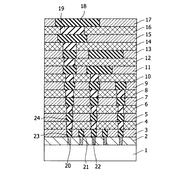
図1において、基板1は、Si基板、SOI(Si・オン・インシュレータ)基板等のSi半導体基板であるが、SiGeやGaAs等々の化合物半導体基板であってもよい。層間絶縁膜として、コンタクト層の層間絶縁膜2と、配線層の層間絶縁膜3、5、7、9、11、13、15、17と、ビア層の層間絶縁膜4、6、8、10、12、14、16を示す。最下層の配線層の層間絶縁膜3から最上層の配線層の層間絶縁膜17までの配線層を順に略称でM1、M2、M3、M4、M5、M6、M7、M8と呼ぶ。最下層のビア層の層間絶縁膜4から最上層のビア層の層間絶縁膜16までのビア層を順に略称でV1、V2、V3、V4、V5、V6、V7と呼ぶ。いくつかの金属配線には18と21〜24の番号を付したが、番号が省略されていてもこれらと同じ模様の部分は金属配線を示す。ビアプラグ19は、金属により構成される。通常、銅配線の場合には銅が用いられる。図中、番号が省略されていても、これと同じ模様の部分はビアプラグを示している。コンタクトプラグ20は、基板1の最上面に形成されたトランジスタ(図示外)のゲートあるいは基板へ接続される。このように、配線層とビア層は交互に積み重なった構成となっており、一般に、多層配線とはM1から上層部分のことを指す。通常、M1〜M3をローカル配線、M4とM5を中間配線あるいはセミグローバル配線、M6〜M8をグローバル配線と呼ぶことが多い。
【0037】
本発明の半導体装置は、配線層の層間絶縁膜3、5、7、9、11、13、15、17、もしくはビア層の層間絶縁膜4、6、8、10、12、14、16の少なくとも1以上の層に、本発明の多孔質膜を用いたものである。
例えば、配線層(M1)の層間絶縁膜3に本発明の多孔質膜を用いている場合、金属配線21と金属配線22の間の配線間容量が大きく低減できる。また、ビア層(V1)の層間絶縁膜4に本発明の多孔質膜を用いている場合、金属配線23と金属配線24の間の配線間容量を大きく低減することができる。このように、配線層に本発明の低比誘電率を有する多孔質膜を用いると、同一層の金属配線間容量を大きく低減できる。また、ビア層に本発明の低比誘電率を有する多孔質膜を用いると、上下金属配線の層間容量を大きく低減できる。
したがって、すべての配線層及びビア層に本発明の多孔質膜を用いることにより、配線の寄生容量を大きく低減できる。本発明の多孔質膜を配線の絶縁膜として使用することにより、従来問題となっていた多孔質膜を積層形成して多層配線を形成する際の多孔質膜の吸湿による誘電率の増大も発生しない。その結果、半導体装置の高速動作及び低消費電力動作が実現される。また、本発明の多孔質膜は機械強度が強いため、半導体装置の機械強度が向上し、その結果半導体装置の製造上の歩留まりや半導体装置の信頼性を大きく向上させることができる。
【0038】
【実施例】
以下、製造例と実施例及び比較例を示し、本発明を具体的に説明するが、本発明は下記の実施例に制限されるものではない。
製造例1
5リットルのフラスコに水640gとエタノール1200gとアニオン交換樹脂65.9ml(総イオン交換容量=2.5meq/ml)を仕込み、25℃でメチルトリメトキシシラン30g(0.22mol)とテトラメトキシシラン40g(0.26mol)を5分間かけて滴下し、その後80℃で3時間撹拌した。次いでプロピレングリコールモノプロピルエーテル400gを加え40℃/20mmHgの条件下で メタノールと水を留去し固形分が6.9重量%の重合体溶液420gを得た。
【0039】
製造例2
5リットルのフラスコに水640gとエタノール1200gと28%アンモニア水溶液10gを仕込み、25℃でメチルトリメトキシシラン30g(0.22mol)とテトラメトキシシラン40g(0.26mol)を5分間かけて滴下し、その後80℃で6時間撹拌した。次いでプロピレングリコールモノプロピルエーテル400gを加え40℃/20mmHgの条件下で メタノールと水を留去し固形分が7.1重量%の重合体溶液390gを得た。
【0040】
製造例3
5リットルのフラスコに水640gとエタノール1200gと28%アンモニア水溶液10gを仕込み、25℃でメチルトリメトキシシラン30g(0.22mol)とテトラメトキシシラン40g(0.26mol)を5分間かけて滴下し、その後60℃で3時間撹拌した。次いでプロピレングリコールモノプロピルエーテル400gを加え40℃/20mmHgの条件下で メタノールと水を留去し固形分が5.9重量%の重合体溶液470gを得た。
【0041】
実施例1、比較例1〜2
製造例1〜3で得られた組成物をシリコンウェハー上にスピン塗布後、風乾し、さらに窒素気流下で425℃にて60分間焼成した。塗布条件は1,000〜3,000rpmで1分間とした。得られた膜のモジュラスとハードネスはMTS社製NanoindenterXPを用いて測定した。また比誘電率は日本SSM製自動水銀プローブを用いて測定した。なお、製造例1〜3で得られた重合体の重量平均分子量及び数平均分子量は、GPCを用いポリスチレン換算により得た。結果を表1に示す。
【0042】
【表1】
【発明の効果】
本発明の組成物を用いることによって、低誘電率でありながら、平坦で均一であると共に機械的な強度も高い半導体装置製造に用いるとき層間絶縁膜として最適な膜を形成することが可能になる。また、本発明の組成物から形成される多孔質膜を多層配線の絶縁膜として使用することにより、高性能かつ高信頼性を有する半導体装置を実現することができる。
【図面の簡単な説明】
【図1】本発明の半導体装置の一例の概略断面図である。
【符号の説明】
1 基板
2 コンタクト層の層間絶縁膜
3 配線層(M1)の層間絶縁膜
4 ビア層(V1)の層間絶縁膜
5 配線層(M2)の層間絶縁膜
6 ビア層(V2)の層間絶縁膜
7 配線層(M3)の層間絶縁膜
8 ビア層(V3)の層間絶縁膜
9 配線層(M4)の層間絶縁膜
10 ビア層(V4)の層間絶縁膜
11 配線層(M5)の層間絶縁膜
12 ビア層(V5)の層間絶縁膜
13 配線層(M6)の層間絶縁膜
14 ビア層(V6)の層間絶縁膜
15 配線層(M7)の層間絶縁膜
16 ビア層(V7)の層間絶縁膜
17 配線層(M8)の層間絶縁膜
18 金属配線
19 ビアプラグ
20 コンタクトプラグ
21 金属配線
22 金属配線
23 金属配線
24 金属配線[0001]
TECHNICAL FIELD OF THE INVENTION
The present invention provides a film-forming composition capable of forming a porous film having excellent dielectric properties, adhesion, uniformity of coating film, mechanical strength, and reduced moisture absorption, a method for forming a porous film, and a method for forming a porous film. The present invention relates to a porous film and a semiconductor device incorporating the porous film.
[0002]
[Prior art]
With the progress of high integration of semiconductor integrated circuits, an increase in wiring delay time caused by an increase in wiring capacitance, which is a parasitic capacitance between metal wirings, has hindered performance enhancement of semiconductor integrated circuits. The wiring delay time is a so-called RC delay which is proportional to the product of the resistance of the metal wiring and the capacitance between the wirings. Therefore, in order to reduce the wiring delay time, it is necessary to reduce the resistance of the metal wiring or reduce the capacitance between wirings.
[0003]
As a method of reducing the capacitance between wirings, it is conceivable to lower the relative dielectric constant of an interlayer insulating film formed between metal wirings. For this purpose, a method of forming a porous insulating film has been proposed. . However, vacancies in the film are a factor that lowers the mechanical strength. Therefore, there is a need for an interlayer insulating film material that achieves both low dielectric constant and high strength.
[0004]
As a method of forming a porous film, after synthesizing a precursor of a siloxane polymer containing a thermally unstable organic component, the precursor solution is applied on a substrate to form a coating film, and then heat treatment is performed. There is a method in which the space occupied by the volatilized components is decomposed and volatilized to form holes. However, the insulating film obtained by this method has a problem that volatile components and decomposed products remain, which cause deterioration of electrical characteristics of the insulating film and an interface peeling phenomenon during a semiconductor device manufacturing process.
[0005]
In addition, it includes a high molecular weight siloxane polymer obtained by hydrolyzing and condensing a silane compound in the presence of an alkali catalyst and a low to medium molecular weight siloxane polymer obtained by hydrolyzing and condensing a silane compound in the presence of an acid catalyst. Although a composition (Patent Document 1) has been proposed, the reduction of the relative dielectric constant is insufficient. Further, a high molecular weight siloxane polymer obtained by hydrolyzing and condensing a silane compound in the presence of an organic base or an inorganic base has been proposed, but the film strength is insufficient.
[0006]
As described above, the conventional materials have a problem that the film quality is deteriorated in the heat treatment step and the cost is increased. In addition, there is a problem that it is difficult to reduce the dielectric constant because the pore diameter increases when forming a porous film. Further, when a conventional porous film is incorporated as an insulating film into a multilayer wiring of a semiconductor device, there is a problem that mechanical strength required for manufacturing the semiconductor device cannot be obtained.
As described above, when the relative permittivity of the porous film used as the insulating film in the multilayer wiring of the semiconductor device is large, the RC delay in the multilayer wiring of the semiconductor device is increased, and the performance (high speed, low power consumption) of the semiconductor device is improved. There was a big problem that could not be achieved. Further, if the mechanical strength of the porous film is weak, there is a problem that the reliability of the semiconductor device is reduced.
[0007]
[Patent Document 1]
JP 2001-164186 A
[Problems to be solved by the invention]
An object of the present invention is to provide a film-forming composition capable of forming a porous film having high strength and a low dielectric constant, a method for producing the same, a method for forming a porous film, and a porous film. Another object of the present invention is to provide a semiconductor device having high performance and high reliability incorporating the porous film.
[0009]
[Means for Solving the Problems]
The present inventors have found that in the case of an insulating film formed from a composition mainly containing a siloxane polymer having a small molecular weight dispersity and not containing porogen, a relative permittivity is high when the molecular weight of the siloxane polymer is large. It has been found that the film strength is low, but the film strength is low, and conversely, if the molecular weight is low, the relative dielectric constant increases, but the film strength decreases. This is thought to be because a high molecular weight siloxane polymer is hindered from aggregating molecules by steric hindrance when the solvent is volatilized, so that pores are likely to be generated between molecules, but the film strength is reduced due to a small number of crosslinkable reactive groups. On the other hand, when the molecular weight of the siloxane polymer is small, it is considered that the film is densely aggregated when the solvent is volatilized, and that the film strength is increased because there are many crosslinkable reactive groups.
[0010]
The present inventors have found that a composition containing a polymer obtained by hydrolyzing a hydrolyzable silane compound in the presence of an anion-type ion exchange resin forms a film having a low dielectric constant and a high strength, Specifically, one or more hydrolyzable silane compounds selected from hydrolyzable silane compounds represented by the following general formulas (1) and (2) are hydrolyzed and condensed in the presence of an anion-type ion exchange resin. It has been found that when a film-forming composition containing the obtained polymer is used, a uniform and flat porous film having a relative dielectric constant of 2.2 or less and a film modulus of 5 Gpa or more can be formed.
[0011]
(R 1 ) a Si (R 2 ) 4-a (1)
(R 3) b (R 5 ) 3-b Si-R 7 -Si (R 6) 3-c (R 4) c (2)
In the above formula, R 1 , R 3 , and R 4 each independently represent a substituted or unsubstituted monovalent hydrocarbon group; R 2 , R 5 , and R 6 each independently represent a hydrolyzable group; 7 represents a divalent organic group, a represents an integer of 0 to 3, and b and c represent an integer of 1 or 2.
[0012]
Accordingly, the present invention provides a film-forming composition containing a polymer obtained by hydrolyzing a hydrolyzable silane compound in the presence of an anionic ion exchange resin, and a hydrolyzable composition in the presence of an anionic ion exchange resin. A method for producing a film-forming composition containing a polymer obtained by hydrolyzing and condensing a silane compound, and applying the composition to a substrate and drying and heating a film formed at a curing temperature or higher. The present invention provides a method for forming a porous film, and a porous film obtained by the method.
[0013]
The semiconductor device of the present invention comprises a polymer obtained by hydrolyzing and condensing at least one hydrolyzable silane compound selected from the group consisting of the following general formulas (1) and (2) in the presence of an anion-type ion exchange resin. A porous film formed using the film-forming composition including the coalesced is provided inside.
(R 1 ) a Si (R 2 ) 4-a (1)
(R 3) b (R 5 ) 3-b Si-R 7 -Si (R 6) 3-c (R 4) c (2)
(In the above formula, R 1 , R 3 and R 4 independently represent a monovalent hydrocarbon group which may have a substituent, and R 2 , R 5 and R 6 independently represent a hydrolyzable group R 7 represents a divalent organic group, a represents an integer of 0 to 3, and b and c represent an integer of 1 or 2.)
Specifically, the porous film is used as an insulating film of a multilayer wiring of a semiconductor device.
In this case, the mechanical strength of the semiconductor device is ensured, and the hygroscopicity of the porous film is reduced, so that a semiconductor device incorporating a low dielectric constant insulating film is realized. With the lowering of the dielectric constant of the insulating film, the parasitic capacitance around the multilayer wiring is reduced, and high-speed operation and low power consumption operation of the semiconductor device are achieved.
Further, in the semiconductor device of the present invention, it is preferable that a porous film is present in an insulating film between metal wirings of the same layer of the multilayer wiring or an interlayer insulating film of the upper and lower metal wiring layers. Thus, a semiconductor device having high performance and high reliability is realized.
[0014]
BEST MODE FOR CARRYING OUT THE INVENTION
Hereinafter, the present invention will be described in detail.
In the hydrolyzable silane compound represented by the general formula (1), R 1 is a monovalent hydrocarbon group which may have a substituent, and preferably has 1 to 12 carbon atoms, and includes an alkyl group, an aryl group, and an aralkyl group. Examples include groups, alkenyl groups, epoxy-containing groups, amino-containing groups, and groups in which some or all of these hydrogen atoms have been substituted with halogen atoms. It preferably has 1 to 6 carbon atoms, and specific examples include a methyl group, an ethyl group, a propyl group, and a phenyl group.
[0015]
In the general formula (1), R 2 represents a monovalent hydrolyzable group, and is a halogen atom, an alkoxy group, an acyloxy group, an oxime group, an amino group, or the like, and preferably controls hydrolysis and condensation reactions. For simplicity, it is an alkoxy group having 1 to 6 carbon atoms, and specific examples of the alkoxy group include a methoxy group, an ethoxy group, a propoxy group, an isopropoxy group, a butoxy group, and an isobutoxy group.
[0016]
Examples of the hydrolyzable silane compound of the general formula (1) include trichlorosilane, trimethoxysilane, triethoxysilane, tripropoxysilane, methyltrichlorosilane, methyltrimethoxysilane, methyltriethoxysilane, methyltripropoxysilane, Ethyltrichlorosilane, ethyltrimethoxysilane, ethyltriethoxysilane, propyltrichlorosilane, propyltrimethoxysilane, phenyltrichlorosilane, phenyltrimethoxysilane, phenyltriethoxysilane, and the like, but are not limited thereto. .
[0017]
In the hydrolyzable silane compound of the general formula (2), R 3 and R 4 are a monovalent hydrocarbon group which may have a substituent, and preferably have 1 to 12 carbon atoms which may have a substituent. Represents a linear or branched alkyl group or aryl group, and may have a substituent. Specific examples of R 3 and R 4 are the same as those exemplified for R 1 .
[0018]
In the hydrolyzable silane compound of the general formula (2), R 5 and R 6 each represent a monovalent hydrolyzable group, such as a halogen atom, an alkoxy group, an acyloxy group, an oxime group, and an amino group. Specific examples of R 5 and R 6 are the same as those exemplified for R 2 .
[0019]
In the hydrolyzable silane compound of the general formula (2), R 7 represents a divalent organic group, and is a linear, branched or cyclic, saturated or unsaturated divalent aliphatic carbon having 1 to 6 carbon atoms. Examples thereof include a hydrogen group, or a divalent aromatic hydrocarbon group having 6 to 12 carbon atoms, such as a monocyclic ring, a condensed polycyclic ring, a bridged ring, or a ring assembly type.
[0020]
Examples of the hydrolyzable silane compound of the general formula (2) include bis (trimethoxysilyl) methane, bis (triethoxysilyl) methane, bis (methyldimethoxysilyl) methane, bis (methyldiethoxysilyl) methane, and bis (methyldiethoxysilyl) methane. (Dimethoxysilyl) methane, bis (diethoxysilyl) methane, bis (dimethylsilyl) methane, bis (dimethylmethoxysilyl) methane, bis (dimethylethoxysilyl) methane, bis-1,2- (trimethoxysilyl) ethane, Bis-1,2- (triethoxysilyl) ethane, bis-1,2- (methyldimethoxysilyl) ethane, bis-1,2- (methyldiethoxysilyl) ethane, bis-1,2- (methylmethoxysilyl) ) Ethane, bis-1,2- (methylethoxysilyl) ethane, bis-1,2- (dimethoxy Lyl) ethane, bis-1,2- (diethoxysilyl) ethane, bis-1,2- (dimethylsilyl) ethane, bis-1,2- (dimethylmethoxysilyl) ethane, bis-1,2- (dimethyl Ethoxysilyl) ethane, bis-1,6- (trimethoxysilyl) hexane, bis-1,6- (triethoxysilyl) hexane, bis-1,6- (methyldimethoxysilyl) hexane, bis-1,6- (Methyldiethoxysilyl) hexane, bis-1,6- (methylmethoxysilyl) hexane, bis-1,6- (methylethoxysilyl) hexane, bis-1,6- (dimethoxysilyl) hexane, bis-1, 6- (diethoxysilyl) hexane, bis-1,6- (dimethylsilyl) hexane, bis-1,6- (dimethylmethoxysilyl) hexane, bis 1,6- (dimethylethoxysilyl) hexane, bis-1,4- (trimethoxysilyl) benzene, bis-1,4- (triethoxysilyl) benzene, bis-1,4- (methyldimethoxysilyl) benzene, Bis-1,4- (methyldiethoxysilyl) benzene, bis-1,4- (methylmethoxysilyl) benzene, bis-1,4- (methylethoxysilyl) benzene, bis-1,4- (dimethoxysilyl) Benzene, bis-1,4- (diethoxysilyl) benzene, bis-1,4- (dimethylsilyl) benzene, bis-1,4- (dimethylmethoxysilyl) benzene, bis-1,4- (dimethylethoxysilyl) ) Benzene and the like.
[0021]
The polymer obtained by hydrolyzing and condensing a hydrolyzable silane compound in the presence of an anion-type ion exchange resin has a wide molecular weight distribution and contains high molecular weight polymers. High film strength and low dielectric constant It is preferable in satisfying both. Specifically, the ratio of the weight average molecular weight to the number average molecular weight is preferably 5 or more, more preferably 5 to 100, and the weight average molecular weight of the polymer is preferably 10,000 or more, more preferably 10, It is preferably from 000 to 100,000,000. The number average molecular weight and the weight average molecular weight can be obtained in terms of polystyrene using gas permeation chromatography (GPC).
[0022]
As the anion-type ion exchange resin used for the hydrolysis, a commercially available one can be used. Specific examples include a strong basic anion exchange resin such as polystyrene having a tetraalkylammonium group and a weak basic anion exchange resin such as polystyrene having a dialkylamino group or a trialkylamino group. Regarding the amount of the anion-type ion exchange resin, the ion-exchange amount of the anion-type ion exchange resin in a unit volume is preferably 0.1 mol% or more, more preferably 0.1 to 200 mol%, of the hydrolyzable silane compound. If it is less than 0.1 mol%, the hydrolysis rate may be slow, which is not practical.
[0023]
The amount of water used in the hydrolysis is preferably 0.5 mol or more and less than 100 mol per 1 mol of the hydrolyzable group. If the amount is less than 0.5 mol, the molecular weight of the polymer becomes so small that a porous film having a low dielectric constant may not be formed. On the other hand, if it is more than 100 mol, it may be troublesome to remove unnecessary water after hydrolysis, which is not practical.
[0024]
During hydrolysis, an organic solvent may be present in order to maintain the stability of the polymer. Examples of the organic solvent include alcohols having 6 or less carbon atoms, ethylene oxide glycol ethers, propylene oxide glycol ethers, and dialkyl glycol ethers. Particularly, those which are compatible with water are preferable, and specific examples thereof include methanol, ethanol, propanol, isopropanol, butanol, isobutanol, propylene glycol monomethyl ether, propylene glycol monoethyl ether, and propylene glycol monopropyl ether.
[0025]
With respect to the method for producing the film-forming composition, the method of the hydrolysis-condensation reaction is not particularly limited, and the anion-type ion-exchange resin, the hydrolyzable silane compound, and water are put into a reaction vessel to perform hydrolytic condensation, and thereafter, A batch system in which the anion-type ion exchange resin and the polymer solution are separated by filtration, and a continuous system in which a hydrolyzable silane compound and water are continuously supplied to a reaction tower filled with the anion-type ion exchange resin to obtain a polymer solution are used. The reaction temperature at this time is not particularly limited as long as the reaction system is liquid.
[0026]
The resulting polymer solution can be used as it is as a film-forming composition, but a siloxane polymer having a lower molecular weight or a siloxane polymer having a higher molecular weight than the weight-average molecular weight of the polymer obtained for adjusting film properties is used. The coalescing may be added up to 50% by weight of the solid content of the film forming composition.
[0027]
The obtained film-forming composition may be diluted or concentrated or solvent-substituted according to application conditions, firing conditions, and desired film characteristics, to obtain a film thickness of an interlayer insulating film in a general semiconductor device. The solid content is preferably 1 to 30% by weight, and the same solvent as that exemplified as the solvent used at the time of hydrolysis can be used as the dilution or replacement solvent.
[0028]
Further, a surfactant can be added in order to improve the flatness of the surface on which the composition for film formation is applied.
[0029]
The film-forming composition used in the present invention can be manufactured in this manner, but any method can be used as long as it is in the range defined above, and is limited by the manufacturing method. It is not done.
[0030]
To form a film using the film-forming composition of the present invention, first, the composition of the present invention is applied on a substrate to form a coating film. Here, examples of the substrate on which the composition of the present invention can be applied include a semiconductor, glass, ceramic, and metal. As a coating method, any method can be used as long as it is a method used in a usual semiconductor device manufacturing, and examples thereof include spin coating, dipping, and a roller blade. Here, the thickness of the coating film to be formed is usually 0.1 to 2 μm in the case of an interlayer insulating film. Next, the formed coating film is heated. The purpose of this method is to evaporate the solvent in the coating solution and fix the shape of the coating film in a step usually called prebaking. The heating temperature at this time is a temperature sufficient to evaporate the solvent in the coating solution.
[0031]
By heating the film thus formed to a temperature sufficient to cure the polymer, a cured film having pores can be formed.
As this method, it is preferable to heat at a temperature of 200 to 500 ° C., and in the case of the present composition, a porous film having pores is obtained. The heating time is about 1 minute to 2 hours, more preferably 5 minutes to 1 hour. If the heating temperature is too low, only a film having insufficient mechanical strength may be produced due to insufficient curing, and a temperature that is too high may not be suitable for a semiconductor device manufacturing process, and a temperature of 300 to 450 ° C. is more preferable. .
[0032]
When the heating is performed in the air or in an inert gas atmosphere, the distribution of the pores of the film and the mechanical strength are different, but by controlling this, the physical properties of the film can be controlled. It is possible and any type can be used without limitation.
Further, in the method for forming a film of the present invention, by heating (reacting) the composition for forming a porous film under reduced pressure, the influence of oxygen is eliminated, and the relative dielectric constant of the obtained film is reduced to a lower value. can do.
[0033]
The film obtained by heating the composition of the present invention by the method of the present invention usually has pores of 10 nm or less, and has a porosity of 5 to 70%. The relative dielectric constant of the film is usually from 2.4 to 1.7. Therefore, the film of the present invention is suitable as an insulating film, and particularly suitable as an interlayer insulating film for a highly integrated circuit.
[0034]
The porous film of the present invention is particularly preferable as an interlayer insulating film for wiring in a semiconductor device. In a semiconductor device, it is necessary to reduce a wiring capacitance in order to prevent a wiring delay even when the integration is increased. Various means have been considered to achieve this, but one of them is to lower the relative dielectric constant of an interlayer insulating film formed between metal wirings.
When an interlayer insulating film is manufactured using the composition for forming a porous film of the present invention, miniaturization and high-speed operation of a semiconductor device can be achieved, and power consumption can be reduced.
[0035]
In the case where the film is made porous by introducing holes to reduce the dielectric constant, there is a problem that the mechanical strength of the film decreases because the density of the material constituting the film decreases. The decrease in mechanical strength not only affects the strength of the semiconductor device itself, but also causes a problem in that the semiconductor device does not have sufficient strength in a chemical mechanical polishing process generally used in a manufacturing process, thereby causing peeling. In particular, when the porous film according to the present invention is used as an interlayer insulating film in a multilayer wiring of a semiconductor device, since the porous film has large mechanical strength, it does not cause such peeling, and thus is manufactured. The reliability of the semiconductor device is greatly improved.
[0036]
An embodiment of the semiconductor device of the present invention will be described. FIG. 1 is a schematic sectional view of an example of the semiconductor device of the present invention.
In FIG. 1, the
[0037]
According to the semiconductor device of the present invention, the
For example, when the porous film of the present invention is used for the
Therefore, by using the porous film of the present invention for all the wiring layers and the via layers, the parasitic capacitance of the wiring can be greatly reduced. The use of the porous film of the present invention as an insulating film for wiring also causes an increase in dielectric constant due to moisture absorption of the porous film when forming a multilayer wiring by stacking porous films, which has conventionally been a problem. do not do. As a result, high speed operation and low power consumption operation of the semiconductor device are realized. Further, since the porous film of the present invention has high mechanical strength, the mechanical strength of the semiconductor device is improved, and as a result, the yield in manufacturing the semiconductor device and the reliability of the semiconductor device can be greatly improved.
[0038]
【Example】
Hereinafter, the present invention will be described specifically with reference to Production Examples, Examples, and Comparative Examples, but the present invention is not limited to the following Examples.
Production Example 1
A 5-liter flask was charged with 640 g of water, 1200 g of ethanol, and 65.9 ml of anion exchange resin (total ion exchange capacity = 2.5 meq / ml), and at 25 ° C., 30 g (0.22 mol) of methyltrimethoxysilane and 40 g of tetramethoxysilane. (0.26 mol) was added dropwise over 5 minutes, followed by stirring at 80 ° C. for 3 hours. Then, 400 g of propylene glycol monopropyl ether was added, and methanol and water were distilled off under the conditions of 40 ° C./20 mmHg to obtain 420 g of a polymer solution having a solid content of 6.9% by weight.
[0039]
Production Example 2
640 g of water, 1200 g of ethanol and 10 g of a 28% aqueous ammonia solution were charged into a 5-liter flask, and 30 g (0.22 mol) of methyltrimethoxysilane and 40 g (0.26 mol) of tetramethoxysilane were added dropwise at 25 ° C. over 5 minutes, Thereafter, the mixture was stirred at 80 ° C. for 6 hours. Then, 400 g of propylene glycol monopropyl ether was added, and methanol and water were distilled off under the conditions of 40 ° C./20 mmHg to obtain 390 g of a polymer solution having a solid content of 7.1% by weight.
[0040]
Production Example 3
640 g of water, 1200 g of ethanol and 10 g of a 28% aqueous ammonia solution were charged into a 5-liter flask, and 30 g (0.22 mol) of methyltrimethoxysilane and 40 g (0.26 mol) of tetramethoxysilane were added dropwise at 25 ° C. over 5 minutes, Thereafter, the mixture was stirred at 60 ° C. for 3 hours. Then, 400 g of propylene glycol monopropyl ether was added, and methanol and water were distilled off under the conditions of 40 ° C./20 mmHg to obtain 470 g of a polymer solution having a solid content of 5.9% by weight.
[0041]
Example 1, Comparative Examples 1-2
The compositions obtained in Production Examples 1 to 3 were spin-coated on a silicon wafer, air-dried, and further baked at 425 ° C. for 60 minutes under a nitrogen stream. The application condition was 1,000 to 3,000 rpm for 1 minute. The modulus and hardness of the obtained film were measured using Nanoindenter XP manufactured by MTS. The relative permittivity was measured using an automatic mercury probe manufactured by Japan SSM. In addition, the weight average molecular weight and the number average molecular weight of the polymers obtained in Production Examples 1 to 3 were obtained in terms of polystyrene using GPC. Table 1 shows the results.
[0042]
[Table 1]
【The invention's effect】
By using the composition of the present invention, it is possible to form an optimal film as an interlayer insulating film when used for manufacturing a semiconductor device which is flat, uniform and has high mechanical strength while having a low dielectric constant. . Further, by using a porous film formed from the composition of the present invention as an insulating film of a multilayer wiring, a semiconductor device having high performance and high reliability can be realized.
[Brief description of the drawings]
FIG. 1 is a schematic sectional view of an example of a semiconductor device of the present invention.
[Explanation of symbols]
Claims (9)
(R1)aSi(R2)4−a (1)
(R3)b(R5)3−bSi−R7−Si(R6)3−c(R4)c (2)
(上式中、R1、R3、R4は独立して置換基を有してもよい1価の炭化水素基を示し、R2、R5、R6は独立して加水分解性基を示し、R7は2価の有機基を示し、aは0〜3の整数を示し、b及びcは1又は2の整数を示す。)It comprises a polymer obtained by hydrolyzing and condensing one or more kinds of hydrolyzable silane compounds selected from the group consisting of the following general formulas (1) and (2) in the presence of an anionic ion exchange resin. Film forming composition.
(R 1 ) a Si (R 2 ) 4-a (1)
(R 3) b (R 5 ) 3-b Si-R 7 -Si (R 6) 3-c (R 4) c (2)
(In the above formula, R 1 , R 3 and R 4 independently represent a monovalent hydrocarbon group which may have a substituent, and R 2 , R 5 and R 6 each independently represent a hydrolyzable group. R 7 represents a divalent organic group, a represents an integer of 0 to 3, and b and c represent an integer of 1 or 2.)
(R1)aSi(R2)4−a (1)
(R3)b(R5)3−bSi−R7−Si(R6)3−c(R4)c (2)
(上式中、R1、R3、R4は独立して置換基を有してもよい1価の炭化水素基を示し、R2、R5、R6は独立して加水分解性基を示し、R7は2価の有機基を示し、aは0〜3の整数を示し、b及びcは1又は2の整数を示す。)A film-forming composition characterized in that one or more hydrolyzable silane compounds selected from the group consisting of the following general formulas (1) and (2) are hydrolyzed and condensed in the presence of an anionic ion exchange resin. Production method.
(R 1 ) a Si (R 2 ) 4-a (1)
(R 3) b (R 5 ) 3-b Si-R 7 -Si (R 6) 3-c (R 4) c (2)
(In the above formula, R 1 , R 3 and R 4 independently represent a monovalent hydrocarbon group which may have a substituent, and R 2 , R 5 and R 6 independently represent a hydrolyzable group R 7 represents a divalent organic group, a represents an integer of 0 to 3, and b and c represent an integer of 1 or 2.)
(R1)aSi(R2)4−a (1)
(R3)b(R5)3−bSi−R7−Si(R6)3−c(R4)c (2)
(上式中、R1、R3、R4は独立して置換基を有してもよい1価の炭化水素基を示し、R2、R5、R6は独立して加水分解性基を示し、R7は2価の有機基を示し、aは0〜3の整数を示し、b及びcは1又は2の整数を示す。)A film-forming composition comprising a polymer obtained by hydrolyzing and condensing one or more types of hydrolyzable silane compounds selected from the group consisting of the following general formulas (1) and (2) in the presence of an anionic ion exchange resin. A semiconductor device having a porous film formed using an object inside.
(R 1 ) a Si (R 2 ) 4-a (1)
(R 3) b (R 5 ) 3-b Si-R 7 -Si (R 6) 3-c (R 4) c (2)
(In the above formula, R 1 , R 3 and R 4 independently represent a monovalent hydrocarbon group which may have a substituent, and R 2 , R 5 and R 6 independently represent a hydrolyzable group R 7 represents a divalent organic group, a represents an integer of 0 to 3, and b and c represent an integer of 1 or 2.)
Priority Applications (2)
| Application Number | Priority Date | Filing Date | Title |
|---|---|---|---|
| JP2003104772A JP2004307692A (en) | 2003-04-09 | 2003-04-09 | Composition for forming porous film, method for producing porous film, porous film, interlayer insulating film, and semiconductor device |
| US10/819,544 US7357961B2 (en) | 2003-04-09 | 2004-04-07 | Composition for forming porous film, porous film and method for forming the same, interlevel insulator film, and semiconductor device |
Applications Claiming Priority (1)
| Application Number | Priority Date | Filing Date | Title |
|---|---|---|---|
| JP2003104772A JP2004307692A (en) | 2003-04-09 | 2003-04-09 | Composition for forming porous film, method for producing porous film, porous film, interlayer insulating film, and semiconductor device |
Publications (1)
| Publication Number | Publication Date |
|---|---|
| JP2004307692A true JP2004307692A (en) | 2004-11-04 |
Family
ID=33127839
Family Applications (1)
| Application Number | Title | Priority Date | Filing Date |
|---|---|---|---|
| JP2003104772A Pending JP2004307692A (en) | 2003-04-09 | 2003-04-09 | Composition for forming porous film, method for producing porous film, porous film, interlayer insulating film, and semiconductor device |
Country Status (2)
| Country | Link |
|---|---|
| US (1) | US7357961B2 (en) |
| JP (1) | JP2004307692A (en) |
Cited By (2)
| Publication number | Priority date | Publication date | Assignee | Title |
|---|---|---|---|---|
| JP2007119568A (en) * | 2005-10-27 | 2007-05-17 | Shin Etsu Chem Co Ltd | Method for producing high molecular weight organopolysiloxane, composition containing high molecular weight organopolysiloxane, and optical semiconductor device sealed with cured product thereof |
| JP2013036000A (en) * | 2011-08-11 | 2013-02-21 | Shin-Etsu Chemical Co Ltd | Method for producing amino-functional polysiloxane |
Families Citing this family (9)
| Publication number | Priority date | Publication date | Assignee | Title |
|---|---|---|---|---|
| JP3505520B2 (en) * | 2001-05-11 | 2004-03-08 | 松下電器産業株式会社 | Interlayer insulating film |
| US9061317B2 (en) | 2002-04-17 | 2015-06-23 | Air Products And Chemicals, Inc. | Porogens, porogenated precursors and methods for using the same to provide porous organosilica glass films with low dielectric constants |
| US8293001B2 (en) * | 2002-04-17 | 2012-10-23 | Air Products And Chemicals, Inc. | Porogens, porogenated precursors and methods for using the same to provide porous organosilica glass films with low dielectric constants |
| US8951342B2 (en) | 2002-04-17 | 2015-02-10 | Air Products And Chemicals, Inc. | Methods for using porogens for low k porous organosilica glass films |
| JP2004307693A (en) * | 2003-04-09 | 2004-11-04 | Shin Etsu Chem Co Ltd | Composition for forming porous film, method for producing porous film, porous film, interlayer insulating film, and semiconductor device |
| US8053159B2 (en) | 2003-11-18 | 2011-11-08 | Honeywell International Inc. | Antireflective coatings for via fill and photolithography applications and methods of preparation thereof |
| US8197757B2 (en) * | 2006-07-07 | 2012-06-12 | Drexel University | Electrical insulation of devices with thin layers |
| US8642246B2 (en) | 2007-02-26 | 2014-02-04 | Honeywell International Inc. | Compositions, coatings and films for tri-layer patterning applications and methods of preparation thereof |
| WO2015027147A1 (en) * | 2013-08-22 | 2015-02-26 | Oregon State University | Hydrolysis deposition |
Family Cites Families (61)
| Publication number | Priority date | Publication date | Assignee | Title |
|---|---|---|---|---|
| JPS61170588A (en) * | 1985-01-25 | 1986-08-01 | Tama Kagaku Kogyo Kk | Production of quaternary ammonium hydroxide |
| JPS6315355A (en) | 1986-07-07 | 1988-01-22 | Fujitsu Ltd | Program loading system |
| JPH05125191A (en) | 1991-11-06 | 1993-05-21 | Kanegafuchi Chem Ind Co Ltd | Silicon hybrid material |
| JPH06145599A (en) | 1992-11-06 | 1994-05-24 | Toray Ind Inc | Coating composition |
| US5494859A (en) * | 1994-02-04 | 1996-02-27 | Lsi Logic Corporation | Low dielectric constant insulation layer for integrated circuit structure and method of making same |
| JPH09194298A (en) | 1995-04-25 | 1997-07-29 | Rikagaku Kenkyusho | Silica-surfactant nanocomposite and method for producing the same |
| US5707783A (en) * | 1995-12-04 | 1998-01-13 | Complex Fluid Systems, Inc. | Mixtures of mono- and DI- or polyfunctional silanes as silylating agents for top surface imaging |
| US6143855A (en) * | 1997-04-21 | 2000-11-07 | Alliedsignal Inc. | Organohydridosiloxane resins with high organic content |
| US6391999B1 (en) * | 1998-02-06 | 2002-05-21 | Rensselaer Polytechnic Institute | Epoxy alkoxy siloxane oligomers |
| JPH11246665A (en) | 1998-02-27 | 1999-09-14 | Japan Science & Technology Corp | Self-retaining porous silica and method for producing the same |
| JP2000044875A (en) | 1998-05-18 | 2000-02-15 | Jsr Corp | Composition for forming film, method for forming film, and low-density film |
| US6037275A (en) * | 1998-08-27 | 2000-03-14 | Alliedsignal Inc. | Nanoporous silica via combined stream deposition |
| KR100618301B1 (en) | 1998-09-01 | 2006-08-31 | 쇼꾸바이 카세이 고교 가부시키가이샤 | Coating liquid and substrate coated with the film for forming silica-comprising film having low dielectric constant |
| WO2000015552A1 (en) * | 1998-09-10 | 2000-03-23 | Nissan Chemical Industries, Ltd. | Moniliform silica sol, process for producing the same, and ink-jet recording medium |
| JP2000309751A (en) | 1999-04-27 | 2000-11-07 | Jsr Corp | Composition for forming film and material for forming insulating film |
| JP2000309753A (en) | 1999-04-27 | 2000-11-07 | Jsr Corp | Composition for forming film and material for forming insulating film |
| JP2001049179A (en) | 1999-06-01 | 2001-02-20 | Jsr Corp | Film forming composition, film forming method, and low density film |
| JP2001049178A (en) | 1999-06-01 | 2001-02-20 | Jsr Corp | Film forming composition, film forming method, and low density film |
| DE60021476T2 (en) * | 1999-06-04 | 2006-05-24 | Jsr Corp. | Coating composition for film production and material for insulating layers |
| JP2000345041A (en) | 1999-06-04 | 2000-12-12 | Jsr Corp | Composition for forming film, method for producing composition for forming film, and material for forming insulating film |
| JP2001002993A (en) | 1999-06-24 | 2001-01-09 | Jsr Corp | Film forming composition, film forming method, and low density film |
| US6696538B2 (en) * | 1999-07-27 | 2004-02-24 | Lg Chemical Ltd. | Semiconductor interlayer dielectric material and a semiconductor device using the same |
| JP2001115028A (en) | 1999-08-12 | 2001-04-24 | Jsr Corp | Composition for forming film, method for forming film, and silica-based film |
| JP3733824B2 (en) | 1999-08-12 | 2006-01-11 | Jsr株式会社 | Method for producing coating liquid for forming silica-based film |
| JP2001055554A (en) | 1999-08-20 | 2001-02-27 | Jsr Corp | Composition for forming film and material for forming insulating film |
| US6197913B1 (en) * | 1999-08-26 | 2001-03-06 | Dow Corning Corporation | Method for making microporous silicone resins with narrow pore-size distributions |
| JP2001080915A (en) | 1999-09-09 | 2001-03-27 | Matsushita Electric Ind Co Ltd | Method for manufacturing porous body |
| JP4804616B2 (en) | 1999-09-20 | 2011-11-02 | 株式会社豊田中央研究所 | Porous body and method for producing the same |
| JP2001098218A (en) | 1999-09-28 | 2001-04-10 | Hitachi Chem Co Ltd | Silica-base coating film, method of forming silica-base coating film and electronic component having silica-base coating film |
| JP4662000B2 (en) | 1999-09-29 | 2011-03-30 | Jsr株式会社 | Film forming composition, film forming method, and insulating film |
| JP2001115021A (en) | 1999-10-18 | 2001-04-24 | Asahi Kasei Corp | Silica precursor / organic polymer composition |
| US6359096B1 (en) * | 1999-10-25 | 2002-03-19 | Dow Corning Corporation | Silicone resin compositions having good solution solubility and stability |
| US6313045B1 (en) * | 1999-12-13 | 2001-11-06 | Dow Corning Corporation | Nanoporous silicone resins having low dielectric constants and method for preparation |
| JP4524822B2 (en) | 1999-10-29 | 2010-08-18 | 株式会社豊田中央研究所 | Method for producing highly crystalline silica mesoporous film |
| US6592980B1 (en) | 1999-12-07 | 2003-07-15 | Air Products And Chemicals, Inc. | Mesoporous films having reduced dielectric constants |
| JP2001203197A (en) | 2000-01-21 | 2001-07-27 | Jsr Corp | Film and method of forming film |
| US20030104225A1 (en) * | 2000-02-01 | 2003-06-05 | Jsr Corporation | Process for producing silica-based film, silica-based film, insulating film, and semiconductor device |
| JP4195773B2 (en) * | 2000-04-10 | 2008-12-10 | Jsr株式会社 | Composition for forming interlayer insulating film, method for forming interlayer insulating film, and silica-based interlayer insulating film |
| US6413647B1 (en) * | 2000-02-28 | 2002-07-02 | Jsr Corporation | Composition for film formation, method of film formation, and silica-based film |
| JP4453148B2 (en) | 2000-02-28 | 2010-04-21 | Jsr株式会社 | Film forming composition and insulating film forming material |
| US7128976B2 (en) * | 2000-04-10 | 2006-10-31 | Jsr Corporation | Composition for film formation, method of film formation, and silica-based film |
| US6852299B2 (en) * | 2000-04-28 | 2005-02-08 | Mitsui Chemicals, Inc. | Water-repellent porous silica, method for preparation thereof and use thereof |
| JP4117439B2 (en) | 2000-05-15 | 2008-07-16 | Jsr株式会社 | Film-forming composition and silica-based film |
| JP4530113B2 (en) | 2000-07-06 | 2010-08-25 | Jsr株式会社 | Method for producing film-forming composition, film-forming composition, film-forming method, and silica-based film |
| JP2002020689A (en) | 2000-07-07 | 2002-01-23 | Jsr Corp | Process for producing film forming composition, film forming composition, film forming process and silica film |
| JP4247592B2 (en) | 2000-07-13 | 2009-04-02 | 信越化学工業株式会社 | Resist material and pattern forming method |
| JP4021131B2 (en) | 2000-07-14 | 2007-12-12 | 触媒化成工業株式会社 | Coating liquid for forming low dielectric constant silica-based coating and substrate with low dielectric constant silica-based coating |
| KR100382702B1 (en) * | 2000-09-18 | 2003-05-09 | 주식회사 엘지화학 | Method for preparing organic silicate polymer |
| JP2001131479A (en) | 2000-10-30 | 2001-05-15 | Tokyo Ohka Kogyo Co Ltd | Coating liquid for forming silica-based film |
| US20040047988A1 (en) * | 2000-11-17 | 2004-03-11 | Jin-Kyu Lee | Poly(methylsilsesquioxane) copolymers and preparation method thereof |
| KR100343938B1 (en) * | 2000-11-29 | 2002-07-20 | Samsung Electronics Co Ltd | Preparation method of interlayer insulation membrane of semiconductor |
| JP3654343B2 (en) | 2001-01-15 | 2005-06-02 | 信越化学工業株式会社 | Film forming composition, method for producing the same, method for forming porous film, and porous film |
| JP4855582B2 (en) * | 2001-02-09 | 2012-01-18 | 日本碍子株式会社 | Mesoporous silica, mesoporous silica composite and production method thereof |
| US6533855B1 (en) * | 2001-02-13 | 2003-03-18 | Novellus Systems, Inc. | Dispersions of silicalite and zeolite nanoparticles in nonpolar solvents |
| EP1245642B1 (en) | 2001-03-27 | 2005-06-08 | Samsung Electronics Co., Ltd. | Siloxane-based resin and method for forming an insulating film between interconnecting layers in wafers |
| US6596404B1 (en) * | 2001-07-26 | 2003-07-22 | Dow Corning Corporation | Siloxane resins |
| US20030064321A1 (en) * | 2001-08-31 | 2003-04-03 | Arch Specialty Chemicals, Inc. | Free-acid containing polymers and their use in photoresists |
| WO2003052003A1 (en) | 2001-12-14 | 2003-06-26 | Asahi Kasei Kabushiki Kaisha | Coating composition for forming low-refractive index thin layers |
| WO2003088344A1 (en) | 2002-04-10 | 2003-10-23 | Honeywell International, Inc. | Low metal porous silica dielectric for integral circuit applications |
| JP4180417B2 (en) * | 2003-03-27 | 2008-11-12 | 信越化学工業株式会社 | Composition for forming porous film, method for producing porous film, porous film, interlayer insulating film, and semiconductor device |
| US20050260420A1 (en) * | 2003-04-01 | 2005-11-24 | Collins Martha J | Low dielectric materials and methods for making same |
-
2003
- 2003-04-09 JP JP2003104772A patent/JP2004307692A/en active Pending
-
2004
- 2004-04-07 US US10/819,544 patent/US7357961B2/en not_active Expired - Fee Related
Cited By (2)
| Publication number | Priority date | Publication date | Assignee | Title |
|---|---|---|---|---|
| JP2007119568A (en) * | 2005-10-27 | 2007-05-17 | Shin Etsu Chem Co Ltd | Method for producing high molecular weight organopolysiloxane, composition containing high molecular weight organopolysiloxane, and optical semiconductor device sealed with cured product thereof |
| JP2013036000A (en) * | 2011-08-11 | 2013-02-21 | Shin-Etsu Chemical Co Ltd | Method for producing amino-functional polysiloxane |
Also Published As
| Publication number | Publication date |
|---|---|
| US7357961B2 (en) | 2008-04-15 |
| US20040202874A1 (en) | 2004-10-14 |
Similar Documents
| Publication | Publication Date | Title |
|---|---|---|
| CN101624698B (en) | Aminosilane used for shallow trench isolation thin film | |
| WO2004044074A1 (en) | Composition for porous film formation, porous film, process for producing the same, interlayer insulation film and semiconductor device | |
| KR100579855B1 (en) | Coating composition for insulating film production, preparation method of insulation film by using the same, insulation film for semi-conductor device prepared therefrom, and semi-conductor device comprising the same | |
| JP2002363285A (en) | Siloxane-based resin and method for forming semiconductor interlayer insulating film using the same | |
| CN1657530A (en) | Multi-functional linear siloxane compound, a siloxane polymer prepared from the compound, and a process for forming a dielectric film by using the polymer | |
| JP4049775B2 (en) | Organosilicate polymer and insulating film containing the same | |
| JP4465181B2 (en) | Composition for forming porous interlayer insulating film and method for producing interlayer insulating film | |
| JP4180417B2 (en) | Composition for forming porous film, method for producing porous film, porous film, interlayer insulating film, and semiconductor device | |
| CN1680466A (en) | Method for forming interlayer dielectric film for semiconductor device using polyhedral molecular silsesquioxane | |
| CN100393777C (en) | Siloxane-based resin and interlayer insulating film of semiconductor produced therefrom | |
| JP2004307692A (en) | Composition for forming porous film, method for producing porous film, porous film, interlayer insulating film, and semiconductor device | |
| EP1412434B1 (en) | Siloxane resins | |
| CN100422241C (en) | Siloxane-based resin and interlayer insulating film of semiconductor device manufactured using the same | |
| JP4139710B2 (en) | Composition for forming porous film, method for producing porous film, porous film, interlayer insulating film, and semiconductor device | |
| CN1759135B (en) | Organosiloxane resin and insulating film using the same | |
| EP1566417B1 (en) | Composition for porous film formation, porous film, process for producing the same, interlayer insulation film and semiconductor device | |
| JP2004307693A (en) | Composition for forming porous film, method for producing porous film, porous film, interlayer insulating film, and semiconductor device | |
| US6908977B2 (en) | Siloxane-based resin and method of forming an insulating film between interconnect layers of a semiconductor device using the same | |
| KR102715082B1 (en) | Composition for forming silica layer, silica layer, and electronic device | |
| KR100450257B1 (en) | Organic silicate polymer and low dielectric insulation film comprising the same | |
| TW202128847A (en) | Curable formulations for forming low-k dielectric silicon-containing films using polycarbosilazane | |
| KR20030057312A (en) | Nanopore forming material for forming insulating film for semiconductors and low dielectric insulating film comprising the same |
Legal Events
| Date | Code | Title | Description |
|---|---|---|---|
| A621 | Written request for application examination |
Free format text: JAPANESE INTERMEDIATE CODE: A621 Effective date: 20050713 |
|
| A977 | Report on retrieval |
Free format text: JAPANESE INTERMEDIATE CODE: A971007 Effective date: 20080501 |
|
| A131 | Notification of reasons for refusal |
Free format text: JAPANESE INTERMEDIATE CODE: A131 Effective date: 20080509 |
|
| A02 | Decision of refusal |
Free format text: JAPANESE INTERMEDIATE CODE: A02 Effective date: 20080909 |