JP2004077887A - Display and electronic equipment having display - Google Patents
Display and electronic equipment having display Download PDFInfo
- Publication number
- JP2004077887A JP2004077887A JP2002239251A JP2002239251A JP2004077887A JP 2004077887 A JP2004077887 A JP 2004077887A JP 2002239251 A JP2002239251 A JP 2002239251A JP 2002239251 A JP2002239251 A JP 2002239251A JP 2004077887 A JP2004077887 A JP 2004077887A
- Authority
- JP
- Japan
- Prior art keywords
- touch panel
- display device
- liquid crystal
- crystal display
- resin filler
- Prior art date
- Legal status (The legal status is an assumption and is not a legal conclusion. Google has not performed a legal analysis and makes no representation as to the accuracy of the status listed.)
- Pending
Links
Images


Landscapes
- Devices For Indicating Variable Information By Combining Individual Elements (AREA)
- Liquid Crystal (AREA)
- Position Input By Displaying (AREA)
Abstract
Description
【0001】
【発明の属する技術分野】
本発明は、画像を表示するための表示装置および表示装置を有する電子機器に関するものである。
【0002】
【従来の技術】
液晶表示パネルは、文字情報や静止画や動画等を表示するために用いられている。この液晶表示パネルの表面には、使用者がたとえば指で触れて入力をできるようにするためのタッチパネルが設けられたものがある。図9(A)、(B)はそのようなタイプの液晶表示パネルの一例の概略構成を示すもので、(A)は分解斜視図、(B)は断面図である。
【0003】
同図において、202はLCD(液晶デバイス)フレーム、204は該LCDフレーム202上に配置されるLCD(液晶デバイス)、206は次に述べるタッチパネル(208)を該LCD204の上方にて稍離間(例えば0.1mm〜1.2mm)して位置した状態で保持するLCDフレーム、208は該LCDフレーム206により上記LCD204の上方にそれと例えば0.1mm〜1.2mm程度の間隔を置いて配置されたタッチパネル、210はそのLCD204とタッチパネル208との間に設けられた空間である。図10はそのタッチパネル208と、LCD204と、その間の空間210とをより詳しく示す断面図である。
【0004】
ところで、上記LCD204とタッチパネル208との間に上記空間210を設けるのは、第1に、ユーザーが入力のためにタッチパネル208に加えた圧力によりLCD204に滲みが生じないようにするためである。
即ち、LCD204とタッチパネル208とをその間に空間210を設けることなく直接接触させる構造だと、図9(B)に示すように入力用ペンPを用いてタッチパネル208を加圧すると、その圧力がもろにLCD204に加わる。すると、LCD208内の液晶が圧力を受けて加圧点からそのまわりに逃げ、それが強い滲みとなって現れるという現象が生じるのである。
【0005】
そこで、空間210を設けると、入力用ペンPを用いてタッチパネル208を加圧したときにLCD208に加わる圧力を顕著に軽減することができ、延いては滲みを軽減することができる。これが空間210を設ける第1の理由なのである。
【0006】
空間210を設ける第2の理由は、タッチパネル208とLCD204との界面にニュートンリング(モアレ縞)が生じないようにするためである。即ち、タッチパネル208とLCD204を直接接しさせることは、図10に示すタッチパネル208のガラス板208gとLCDのガラス板208gが直接接触させることに他ならない。そして、ガラス板208gとLCDのガラス板208gは共に表面がより平面度の高い平面になるように仕上げられているとはいえ、完全な平面ではないので、その界面に微小とはいえ、空気の入った空間がランダムに散在し、その結果、ニュートンリングが生じてしまうのである。
これは表示部から視えるので、表示画像の品位を低下させ、当然のことながら好ましくない。そこで、その間に完全に空間210を介在させるのである。すると、ニュートンリングは生じない。
【0007】
尚、このような問題は、タッチパネル208のガラス板208gとLCDのガラス板208gを一つのガラス板で兼用することができれば、空間210を設けるという手段を講じことなく解決する筈である。しかし、それには、タッチパネル208とLCD204を一体に形成することが必要であり、それは、少なくとも現時点では事実上不可能なのである。というのは、LCD204をつくる工程と、タッチパネル208をつくる工程とは、製造条件、特に温度条件が顕著に異なり、一体化してつくることが難しい乃至不可能であるからである。
従って、少なくとも現在の技術では、タッチパネル208のガラス板208gとLCDのガラス板204gを一つのガラス板で兼用することは不可能であり、従って、その間に空間210を設けることが必要なのである。
【0008】
【発明が解決しようとする課題】
ところが、このように、タッチパネル208とLCD204との間にエアーのギャップ210を設けると、タッチパネル208・LCD204間にエアーのギャップ210が存在することから、タッチパネル208を強く、激しく押した場合には、タッチパネルに割れが生じ易くなり、故障する虞れがある。
【0009】
また、タッチパネル208とLCD204との間にエアーのギャップ210を設けると、タッチパネル208・LCD204の界面での無視できない光の反射が生じ、視認性が悪くなるという問題もある。というのは、タッチパネル208のガラス板とエアーとの屈折率の差が大きいので、タッチパネル208の下部を成すガラス板208g、LCD204の上部を成すガラス板204gと、エアーとの屈折率の差が大きく、ガラス板208gとエアーとの界面、ガラス板204gとエアーとの界面にて反射が生じるからである。
【0010】
そこで本発明は、上記課題を解消し、タッチパネルの強度の向上を図ることができ、かつ表示装置の薄型化を図ることができ、更には、タッチパネルと液晶表示パネルとの間における光の反射を低減することができる表示装置および表示装置を有する電子機器を提供することを目的としている。
【0011】
【課題を解決するための手段】
請求項1の発明は、画像を表示するための表示装置であり、前記画像を表示する液晶表示パネルと、前記液晶表示パネルに対して間隔を設けて配置されて使用者が触れて指令を入力するためのタッチパネルとの間に設けられている前記間隔の領域内に、前記タッチパネルを通じて加わる力を緩衝するための透明樹脂充填材を充填したことを特徴とする表示装置である。
【0012】
請求項1では、液晶表示パネルは画像を表示する。タッチパネルは、液晶表示パネルに対して間隔を設けて配置されており、使用者が触れて指令を入力するためのものである。
該透明樹脂充填材は、液晶表示パネルとタッチパネルの間に設けられている間隔の領域内に設けられる。この樹脂充填材は、基本的には、タッチパネルを通じて液晶表示パネル側に加わる力を緩衝するためのものである。
【0013】
該樹脂充填材は液晶表示パネルの画像表示のにじみを起こさずに光透過率を落とすことなく、タッチパネルの割れを防いでタッチパネルの強度を向上することができるといえる。また、液晶表示パネルとタッチパネルの間の間隔は僅かで済むので、表示装置の薄型化にも有効である。更に、樹脂充填材は、液晶表示パネルとタッチパネルの間にでの光の反射による視認性の低下を低減する役割を果たす。というのは、樹脂充填材は一般にその屈折率がエアーとガラスの屈折率の中間の値を持つので、エアーを介在させず、液晶表示パネルやタッチパネルを成すガラス板と樹脂充填材を直接接するようにした場合の方が従来におけるようにガラス板間にエアーが介在する場合よりもパネル間での光反射をより小さくでき、延いては視認性の低下を軽減することができる。
【0014】
請求項2の発明は、請求項1の記載の表示装置において、樹脂充填材が重合性樹脂組成物からなり、前記樹脂充填材の波長430nm〜700nmの範囲における光透過率が、前記樹脂充填材の膜厚が500μmとした場合に95%以上であることを特徴とする。
【0015】
従って、請求項2の発明によれば、樹脂充填材の波長430nm乃至700nmの範囲では光透過率が、樹脂充填材の膜厚が500μmとした場合には95%以上であるので、樹脂充填材は液晶表示パネルの画像表示のにじみを起こさずに光透過率を落とすことなく、タッチパネルの割れを防いでタッチパネルの強度を向上することができる。また、液晶表示パネルとタッチパネルの間の間隔は僅かで済むので、表示装置の薄型化にも有効である。
【0016】
請求項3の発明は、請求項2に記載の表示装置において、前記重合性樹脂組成物が、樹脂成分として(メタ)アクリレートと光開始剤とを含有する。
【0017】
請求項4の発明は、請求項3に記載の表示装置において、前記樹脂成分は、ウレタン系(メタ)アクリレート、ポリブタジエン系(メタ)アクリレート、およびイソプレン系(メタ)アクリレートを含有する。
【0018】
請求項5の発明は、請求項4に記載の表示装置において、前記光開始剤が、可視領域に吸収のある光開始剤を含む。
【0019】
請求項6の発明は、請求項3に記載の表示装置において、前記光開始剤が、フォスフィンオキサイド系開始剤である。
【0020】
請求項7の発明は、請求項6に記載の表示装置において、前記フォスフィンオキサイド系開始剤が、ビス(2,6−ジメトキシベンゾイル)−2,4,4−トリメチル−ペンチルフォスフィンオキサイド、またはビス(2,4,6−トリメチルベンゾイル)−フェニルフォスフィンオキサイドである。
【0021】
請求項8の発明は、請求項3に記載の表示装置において、前記光開始剤が、2−ベンジル−2−ジメチルアミノ−1−(4−モルフォリノフェニル)−ブタノン−1である。
【0022】
請求項9の発明は請求項1に記載の表示装置において、前記透明樹脂充填材が特殊合成ゴム透明塗料である。
【0023】
請求項10の発明は、画像を表示するための表示装置を有する電子機器であり、前記表示装置は、前記画像を表示する液晶表示パネルと、前記液晶表示パネルに対して間隔を設けて配置されて使用者が触れて指令を入力するためのタッチパネルと、前記液晶表示パネルと前記タッチパネルの間に設けられている前記間隔の領域内に充填されて前記タッチパネルを通じて加わる力を緩衝するための樹脂充填材と、を備え、前記樹脂充填材は重合性樹脂組成物からなることを特徴とする表示装置を有する電子機器である。
【0024】
請求項10では、液晶表示パネルは画像を表示する。タッチパネルは、液晶表示パネルに対して間隔を設けて配置されており、使用者が触れて指令を入力するためのものである。
樹脂充填材は、液晶表示パネルとタッチパネルの間に設けられている間隔の領域内に充填される。この樹脂充填材は、タッチパネルを通じて液晶表示パネル側に加わる力を緩衝するためのものである。
【0025】
請求項11では、この樹脂充填材は重合性樹脂組成物からなり、前記樹脂充填材の波長430nm〜700nmの範囲における光透過率が、前記樹脂充填材の膜厚が500μmとした場合に95%以上である。
これにより、樹脂充填材の波長430nm乃至700nmの範囲では光透過率は、樹脂充填材の膜厚が500μmとした場合には95%以上であるので、樹脂充填材は液晶表示パネルの画像表示のにじみを起こさずに光透過率を落とすことなく、タッチパネルの割れを防いでタッチパネルの強度を向上することができる。また、液晶表示パネルとタッチパネルの間の間隔は僅かで済むので、表示装置の薄型化にも有功である。
【0026】
【発明の実施の形態】
以下、本発明の好適な実施の形態を添付図面に基づいて詳細に説明する。
なお、以下に述べる実施の形態は、本発明の好適な具体例であるから、技術的に好ましい種々の限定が付されているが、本発明の範囲は、以下の説明において特に本発明を限定する旨の記載がない限り、これらの形態に限られるものではない。
【0027】
図1は、本発明の表示装置の第1の実施の形態を有する電子機器の好ましい第1の実施の形態を示している。
図1に示す電子機器10は、一例としていわゆる携帯情報端末(PDA)である。この電子機器10は、筐体12と表示装置14を有している。
図2は、図1の電子機器10をさらに詳しく示している。
図1の電子機器10は、筐体12、表示装置14、入力装置20、およびパワーキー22、音声のボリューム調整部24、外部のイヤーホンをつなぐためのジャック27、他の機能を発揮させるためのキー26,28等を有している。
【0028】
図1の入力装置20は、操作者(使用者)の部位、たとえば手Hの指Fにより操作することでポインタPの座標データを与えるためのものである。指Fは図1の例では人差指を用いているが、これに限らず他の指であっても勿論構わない。図2では、図1の表示画面30に表示した情報40の一例を表示している。図1と図2に示すように表示画面30にはポインタPを表示している。このポインタPは矢印形のポインタである。
図2に示すように表示装置14の表示画面30には、ポインタPの他に、情報40や、各種機能を実施するためのキー44,46,48等が表示されている。キー42はキーボードを表示画面30に表示させるためのキーである。キー44は情報の検索に用いるキーである。キー46はメニューを表示画面30に表示するためのキーである。キー48はたとえば表示を英語表示か日本語表示に切り換えることができるキーである。これらのキー42,44,46,48の操作は指Fでタッチすることで行える。
【0029】
図2の筐体12は、第1部分12Aと第2部分12Bを有している。第1部分12Aは上筐体部分とも呼び、第2部分12Bは下筐体部分とも呼ぶ。第1部分12Aと第2部分12Bは重ねることにより、その中に空間を形成している。この空間には表示装置14や回路基板等が収容されている。
筐体12は、たとえばプラスチックであるABS(アクルロニトリルブタジエンスチレン)、PC(ポリカーボネート)、PC+ABS(ポリカーボネート+アクリロニトリルブタジエンスチレン)、PBT(ポリブチレンテレフタレート)、PPS(ポリフェニレンサルファイド)、変性PPE(ポリフェチレンエーテル)等により作られている。
【0030】
図3は、図1と図2に示す筐体12の中に収容されている表示装置14の構造例を示している。
表示装置14は、液晶表示装置とも呼んでおり、概略的には液晶表示パネル60、第1保持フレーム61、第2保持フレーム62、バックライトユニット63およびタッチパネル64を有している。
液晶表示パネル60は、たとえば液晶層の前後を配向膜および透明電極膜で挟み、さらに透明板および偏光板を積層した一般的な構造のものであり、各種の形式のものを採用できる。この液晶表示パネル60とバックライトユニット63は、駆動回路等が実装された基板(図示せず)に対して電気的に接続されている。第1保持フレーム61と第2保持フレーム62は、液晶表示パネル60を一方側と他方側から挟み込む状態で保持するためのフレームである。第1保持フレーム61と第2保持フレーム62は、プラスチックや金属で作られており、たとえばステンレスや鉄等のプレス加工品である。
【0031】
図4は、液晶表示装置14を含む筐体12の断面図であり、液晶表示パネル60は、上述した第1保持フレーム61と第2保持フレーム62により挟まれて保持されている。
図3に示すように、第1保持フレーム61はたとえば長方形の開口部70を有している。この開口部70は、液晶表示パネル60の表示面積に対応する大きさを有している。
【0032】
第2保持フレーム62は、液晶表示パネル60と同じような大きさの開口部71を有している。従って液晶表示パネル60は、バックライトユニット63に対して接している。
第1保持フレーム61の複数個の凹部73に対して、第2保持フレーム62の複数個の突起74をはめ込むことにより、第1保持フレーム61と第2保持フレーム62は、液晶表示パネル60を挟み込んだ形で保持することができる。
【0033】
バックライトユニット63は、たとえば蛍光管の光源を有しており、この光源からの光を樹脂製等の導光板によって液晶表示パネル60の背面側に導く。この導かれた光は、拡散シートによって拡散してプリズムシートを透過させて、液晶表示パネル60の背面側から光を照射するものである。このようなバックライトユニット63を用いることにより、使用者は液晶表示パネル60に表示している画像表示をより鮮明に見ることができる。
【0034】
図3のタッチパネル64は、たとえばガラスの板やポリエステルフィルムなどの貼りあわせにて作られている。このタッチパネル64は液晶表示パネル60の表示画面30に対応した長方形状を有している。図5に示すようにタッチパネル64と表示画面30の間には、間隔が設けられている。
【0035】
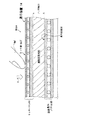
図5は、図4の部分Aを拡大して示している。
図5に示す部分Aは、タッチパネル64と液晶表示パネル60の一部を示しており、タッチパネル64と液晶表示パネル60の表示パネル30の間には、間隔80が設けられている。この間隔80は、たとえば0.8mmであるが、これよりも小さくても勿論構わない。間隔80は、外枠材である図4の第1保持フレーム61により設けられている。つまり、タッチパネル64は第1保持フレーム61に固定されていて、タッチパネル64の内面と液晶表示パネル60の表示画面30の間に間隔80が形成されている。
【0036】
この間隔80の空間領域内には、図4と図5に示すように樹脂充填材90が充填されている。この樹脂充填材90は、光硬化性接着剤ともいい、たとえば可視光硬化性透明接着剤を用いることができる。
この樹脂充填材90としては、たとえばソニーケミカル株式会社製のSOA1000シリーズのものを採用できる。この樹脂充填材90は、間隔80がエアギャップである時にこの間隔80に対して充填される光硬化性樹脂である。すなわち樹脂充填材90は、外枠材である図3に示す第1保持フレーム61と第2保持フレーム62により間隔80が設定されたタッチパネル64と液晶表示パネル60の表示画面30の間に充填される充填材であり、タッチパネル64のタッチ面64Tに加わるたとえば指Fの力を緩衝する作用を有している。
この樹脂充填材90は重合性樹脂組成物からなり、図6に示すように樹脂充填材90の波長430nm〜700nmの範囲における光透過率が、樹脂充填材90の膜厚が500μmとした場合に95%以上である。
【0037】
この重合性樹脂組成物は、樹脂成分として(メタ)アクリレートと光開始剤とを含有する。
この樹脂成分は、ウレタン系(メタ)アクリレート、ポリブタジエン系(メタ)アクリレート、およびイソプレン系(メタ)アクリレートを含有する。
光開始剤は、可視領域に吸収のある光開始剤を含む。
光開始剤は、たとえばフォスフィンオキサイド系開始剤である。このフォスフィンオキサイド系開始剤は、ビス(2,6−ジメトキシベンゾイル)−2,4,4−トリメチル−ペンチルフォスフィンオキサイド、またはビス(2,4,6−トリメチルベンゾイル)−フェニルフォスフィンオキサイドである。
また、光開始剤は、2−ベンジル−2−ジメチルアミノ−1−(4−モルフォリノフェニル)−ブタノン−1であってもよい。
【0038】
上述した樹脂充填材90は、緩衝充填材あるいは樹脂緩衝材とも呼んでいる。樹脂充填材は、視認性の観点から高い透明性を有することと、落下や押圧に対する衝撃を緩和する観点から柔軟性を有することと、および離間された領域内に充填するために製造時には液状であることが必要であり、これら多数の要求を満たすには、要求特性に合わせて配合処方が可能となる、モノマー、オリゴマーを含む樹脂成分と光開始剤を含む重合性樹脂組成物が好ましい。
【0039】
重合性樹脂組成物の樹脂成分は、具体例を挙げると、高い透明性を維持する観点から、脂環構造を有する(メタ)アクリレート、柔軟性を付与する観点からゴム成分を有する(メタ)アクリレートが挙げられ、これらの中でも比較的高い透明性と柔軟性を併せ持つ、ウレタン系(メタ)アクリレート、ポリブタジエン骨格をもつポリブタジエン系(メタ)アクリレート、およびイソプレン骨格を持つイソプレン系(メタ)アクリレートを好ましく挙げることができる。
【0040】
光開始剤は、本発明に係る表示装置14の製造工程を考慮して選択することができる。
すなわち、樹脂緩衝材の母材であるアクリレート等に紫外線等を照射して重合が開始された後、速やかにタッチパネル64を外枠材に載置することが可能である場合には、特に、光開始剤は制限なく使用することができる。
但しこのような方法は、オペレータに熟練を要するため、タッチパネル64を外枠材に載置した後にタッチパネルを介して紫外線等を照射することが製造工程が安定になる。
この場合、タッチパネル64自身は不透明ではないものの、ある程度の厚みを有するため、紫外線等の光強度を高めないと重合率が十分でない場合がある。
【0041】
そこで、本発明においては、可視領域に吸収があり可視領域波長で重合が開始する、いわゆる可視光開始剤を好ましく使用することができる。この可視光開始剤の具体例を挙げると、ビス(2,6−ジメトキシベンゾイル)−2,4,4−トリメチル−ペンチルフォスフィンオキサイド、ビス(2,4,6−トリメチルベンゾイル)−フェニルフォスフィンオキサイド等のフォスフィンオキサイド系光開始剤、2−ベンジル−2−ジメチルアミノ−1−(4−モルフォリノフェニル)−ブタノン−1等が挙げられる。
【0042】
次に、上記の重合性樹脂組成物からなる樹脂緩衝材90は、波長430nm〜700nmにおける光透過率が、樹脂緩衝材90の膜厚を500μmとした場合に、95%以上となるように配合する。
このように樹脂緩衝材90の波長が430nm乃至700nmにおける光透過率が、樹脂緩衝材90の膜厚を500μmとした場合に95%以上になるようにすると、液晶表示パネルにおける画像表示のにじみが起こらず、光透過率を落とさずに、タッチパネル64の割れを防いでタッチパネルの強度アップを図ることができる。しかもこの隙間80の大きさはたとえば0.8mmあるいはそれよりも小さくすることができるので、表示装置14自体の薄型化にも貢献できる。
樹脂緩衝材90は、図5に示す間隔80に充填し、タッチパネル64のR側からたとえば紫外線を照射することで硬化させる。
【0043】
本発明者の実験結果では、従来のエアギャップの間隔を有している表示装置と、本発明の実施の形態のように間隔80に樹脂充填材90が充填された表示装置について、タッチパネルの静荷重での強度比較をしたところ、約2倍の効果が得られた。そして光透過率について従来の表示装置と本発明の実施の形態の表示装置とを比較した場合でも、両者には全く差が見られなかった。
【0044】
液晶表示パネル60の表示画面30における画像表示のにじみについても、樹脂充填材90が存在していてもこのにじみが発生しないことが確認できた。
タッチパネル64が割れるのには、ある一定以上タッチパネル64に対して変異が生じる場合であるが、光硬化性樹脂である樹脂充填材90の存在により、タッチパネル64のR方向からの押圧時の強度をアップさせることができる。
【0045】
当然のことながら、樹脂充填材90の層を薄くすることにより、従来よりも間隔80の大きさを小さくして、かつある程度のタッチパネル64の強度を得ることも可能である。従って表示装置14の全体の厚みの薄型化が可能になる。
本発明の実施の形態の樹脂充填材90は、たとえばガラス製の表示画面30から簡単に離すことも可能であり、この樹脂充填材90は、表示装置14をリサイクルする際に単品で回収できる。このことから、環境にも配慮されている。
【0046】
このように、本発明の表示装置および表示装置を有する電子機器では、タッチパネル64と液晶表示パネル60の表示画面30との間に、たとえば紫外線硬化型の樹脂充填材90を充填することにより、光透過率を落とさずに衝撃等によるタッチパネル64の割れを防いでタッチパネル64の強度をアップすることができる。
そして電子機器および表示装置14をリサイクルもしくは解体する場合には、樹脂充填材90はガラス製の表示画面30およびタッチパネル64から離すことができるので、樹脂充填材90を単品で回収することが可能であり環境に対して配慮されている。
【0047】
図7(A)、(B)は本発明の第2の実施の形態の概略構成を示すもので、(A)は分解斜視図、(B)は断面図であり、図8はタッチパネルと、LCDと、その間に介在する樹脂充填材をより詳しく示す断面図である。
【0048】
図7、図8において、102はLCD(液晶デバイス)フレーム、104は該LCDフレーム102上に配置されるLCD、106は次に述べるタッチパネル(108)を該LCD104の上方にて稍離間(例えば0.1mm〜1.2mm)して位置した状態で保持するLCDフレーム、108は該LCDフレーム106により上記LCD102の上方にそれと例えば1.0mm程度の厚さの樹脂充填材110を介して配置されたタッチパネルである。
【0049】
上記樹脂充填材110は、例えば特殊合成ゴム透明塗料バイクリア(商品名。ハイビーコート株式会社製)からなる。
この例えば特殊合成ゴム透明塗料バイクリアからなる樹脂充填材110は、高い透明性を有するので、表示装置に必要なLCD画面の視認性の低下が低い。また、ゴム弾性を有するので、タッチパネル108にペンPで文字等の入力のため圧力を加えたときのLCD104に加わる荷重を緩和することができ、延いては、実質的に機械的強度を向上させることができるといえる。
【0050】
そして、樹脂充填材110の屈折率は、空気のそれよりも大きくガラス104g、108gのそれに近いので、図9、図10に示すようにタッチパネル(208)・LCD(204)間に空間(210)、換言すれば空気(エアー)を介在させた場合に比較して界面で生じる屈折も小さくできる。その点でも視認性が向上する。
【0051】
ところで本発明は上記実施の形態に限定されるものではない。
本発明の表示装置は、図示の実施の形態では携帯情報端末に搭載される場合が多いかもしれないが、しかし、これに限らずこの本発明の表示装置は、携帯情報端末の他の種類の電子機器、たとえば携帯電話、携帯型のテレビジョン受像機、無線機、カーナビゲーションのような車両案内装置、その他の液晶表示パネルを有する機器に適用できる。
【0052】
【発明の効果】
以上説明したように、本発明によれば、透明性を確保しながらタッチパネルの強度の向上を図ることができ、かつ表示装置の薄型化を図ることができ、更には、タッチパネルと液晶表示パネルとの間における光の反射を低減することができる。
【図面の簡単な説明】
【図1】本発明の第1の実施の形態の表示装置を有する電子機器を示す斜視図。
【図2】図1の電子機器をより詳しく示す斜視図。
【図3】図1と図2に示す電子機器に搭載されている表示装置を示す分解斜視図。
【図4】図3の表示装置の断面図。
【図5】図4の表示装置の部分Aを示す拡大図。
【図6】樹脂緩衝材の透過率のデータの一例を示す図。
【図7】(A)、(B)は本発明の第2の実施の形態の表示装置を示すもので、(A)は分解斜視図、(B)は断面図。
【図8】上記第2の実施の形態の表示装置の要部を示す断面図である。
【図9】(A)、(B)は従来例の表示装置を示すもので、(A)は分解斜視図、(B)は断面図。
【図10】上記従来例の要部を示す断面図である。
【符号の説明】
10・・・電子機器、14・・・表示装置、60・・・液晶表示パネル、61・・・第1保持フレーム、62・・・第2保持フレーム、63・・・バックライトユニット、64・・・タッチパネル、80・・・間隔、90・・・樹脂充填材、102…LCDフレーム、104…液晶表示パネル(LCD)、106…タッチパネルフレーム、108…タッチパネル、110…樹脂充填材。[0001]
TECHNICAL FIELD OF THE INVENTION
The present invention relates to a display device for displaying an image and an electronic apparatus having the display device.
[0002]
[Prior art]
The liquid crystal display panel is used for displaying character information, still images, moving images, and the like. Some liquid crystal display panels are provided with a touch panel on the surface thereof so that a user can make an input by touching with a finger, for example. FIGS. 9A and 9B show a schematic configuration of an example of such a type of liquid crystal display panel, where FIG. 9A is an exploded perspective view and FIG. 9B is a cross-sectional view.
[0003]
In the figure,
[0004]
First, the
That is, in a structure in which the
[0005]
Therefore, when the
[0006]
The second reason for providing the
Since this is visible from the display unit, the quality of the displayed image is degraded, which is of course undesirable. Therefore, the
[0007]
Such a problem should be solved without providing a
Therefore, at least with the current technology, it is impossible to share the glass plate 208g of the
[0008]
[Problems to be solved by the invention]
However, when the
[0009]
In addition, if the
[0010]
Therefore, the present invention solves the above-mentioned problems, can improve the strength of the touch panel, can reduce the thickness of the display device, and can further reduce the reflection of light between the touch panel and the liquid crystal display panel. It is an object of the present invention to provide a display device which can be reduced and an electronic device having the display device.
[0011]
[Means for Solving the Problems]
The invention according to
[0012]
According to the first aspect, the liquid crystal display panel displays an image. The touch panel is disposed at an interval with respect to the liquid crystal display panel, and is used by a user to input a command by touching the touch panel.
The transparent resin filler is provided in a region at an interval provided between the liquid crystal display panel and the touch panel. This resin filler is basically for buffering the force applied to the liquid crystal display panel through the touch panel.
[0013]
It can be said that the resin filler can improve the strength of the touch panel by preventing cracking of the touch panel without lowering the light transmittance without causing blurring of the image display of the liquid crystal display panel. In addition, since the distance between the liquid crystal display panel and the touch panel is small, it is effective for reducing the thickness of the display device. Further, the resin filler plays a role in reducing a decrease in visibility due to reflection of light between the liquid crystal display panel and the touch panel. Because the resin filler generally has a refractive index between the refractive index of air and that of glass, make sure that the glass filler and liquid crystal display panel or touch panel are in direct contact with the resin filler without air. In this case, light reflection between the panels can be made smaller than in the case where air is interposed between the glass plates as in the related art, and the reduction in visibility can be reduced.
[0014]
According to a second aspect of the present invention, in the display device according to the first aspect, the resin filler is made of a polymerizable resin composition, and the resin filler has a light transmittance in a wavelength range of 430 nm to 700 nm. Is not less than 95% when the film thickness is 500 μm.
[0015]
Therefore, according to the second aspect of the present invention, the light transmittance in the wavelength range of 430 nm to 700 nm of the resin filler is 95% or more when the film thickness of the resin filler is 500 μm. Can prevent the touch panel from cracking and improve the strength of the touch panel without causing blurring of the image display of the liquid crystal display panel and reducing the light transmittance. In addition, since the distance between the liquid crystal display panel and the touch panel is small, it is effective for reducing the thickness of the display device.
[0016]
According to a third aspect of the present invention, in the display device according to the second aspect, the polymerizable resin composition contains (meth) acrylate and a photoinitiator as resin components.
[0017]
According to a fourth aspect of the present invention, in the display device according to the third aspect, the resin component contains a urethane (meth) acrylate, a polybutadiene (meth) acrylate, and an isoprene (meth) acrylate.
[0018]
According to a fifth aspect of the present invention, in the display device according to the fourth aspect, the photoinitiator includes a photoinitiator having absorption in a visible region.
[0019]
The invention according to claim 6 is the display device according to
[0020]
The invention according to claim 7 is the display device according to claim 6, wherein the phosphine oxide-based initiator is bis (2,6-dimethoxybenzoyl) -2,4,4-trimethyl-pentylphosphine oxide or Bis (2,4,6-trimethylbenzoyl) -phenylphosphine oxide.
[0021]
The invention according to
[0022]
According to a ninth aspect of the present invention, in the display device according to the first aspect, the transparent resin filler is a special synthetic rubber transparent paint.
[0023]
The invention according to
[0024]
In
The resin filler is filled in an interval region provided between the liquid crystal display panel and the touch panel. This resin filler is for buffering a force applied to the liquid crystal display panel through the touch panel.
[0025]
In claim 11, the resin filler is made of a polymerizable resin composition, and the light transmittance of the resin filler in a wavelength range of 430 nm to 700 nm is 95% when the film thickness of the resin filler is 500 μm. That is all.
As a result, in the wavelength range of 430 nm to 700 nm of the resin filler, the light transmittance is 95% or more when the film thickness of the resin filler is 500 μm. The strength of the touch panel can be improved by preventing cracking of the touch panel without causing bleeding and lowering the light transmittance. In addition, since the distance between the liquid crystal display panel and the touch panel is small, it is also effective for reducing the thickness of the display device.
[0026]
BEST MODE FOR CARRYING OUT THE INVENTION
Hereinafter, preferred embodiments of the present invention will be described in detail with reference to the accompanying drawings.
The embodiments described below are preferred specific examples of the present invention, and therefore, various technically preferable limitations are given. However, the scope of the present invention particularly limits the present invention in the following description. It is not limited to these forms unless otherwise stated.
[0027]
FIG. 1 shows a preferred first embodiment of an electronic apparatus having the first embodiment of the display device of the present invention.
The
FIG. 2 shows the
The
[0028]
The
As shown in FIG. 2, on the
[0029]
2 has a
The housing 12 is made of, for example, plastics such as ABS (acrylonitrile butadiene styrene), PC (polycarbonate), PC + ABS (polycarbonate + acrylonitrile butadiene styrene), PBT (polybutylene terephthalate), PPS (polyphenylene sulfide), and modified PPE (polyfethiene). Renether).
[0030]
FIG. 3 shows a structural example of the display device 14 housed in the housing 12 shown in FIGS. 1 and 2.
The display device 14 is also called a liquid crystal display device, and roughly includes a liquid
The liquid
[0031]
FIG. 4 is a cross-sectional view of the housing 12 including the liquid crystal display device 14. The liquid
As shown in FIG. 3, the
[0032]
The
The
[0033]
The
[0034]
The
[0035]
FIG. 5 shows a portion A of FIG. 4 in an enlarged manner.
A part A shown in FIG. 5 shows a part of the
[0036]
As shown in FIGS. 4 and 5, a
As the
This
[0037]
This polymerizable resin composition contains (meth) acrylate and a photoinitiator as resin components.
This resin component contains urethane (meth) acrylate, polybutadiene (meth) acrylate, and isoprene (meth) acrylate.
Photoinitiators include those that absorb in the visible region.
The photoinitiator is, for example, a phosphine oxide-based initiator. The phosphine oxide-based initiator is bis (2,6-dimethoxybenzoyl) -2,4,4-trimethyl-pentylphosphine oxide or bis (2,4,6-trimethylbenzoyl) -phenylphosphine oxide. is there.
Also, the photoinitiator may be 2-benzyl-2-dimethylamino-1- (4-morpholinophenyl) -butanone-1.
[0038]
The above-described
[0039]
Specific examples of the resin component of the polymerizable resin composition include a (meth) acrylate having an alicyclic structure from the viewpoint of maintaining high transparency, and a (meth) acrylate having a rubber component from the viewpoint of imparting flexibility. Among these, urethane-based (meth) acrylates having relatively high transparency and flexibility, polybutadiene-based (meth) acrylates having a polybutadiene skeleton, and isoprene-based (meth) acrylates having an isoprene skeleton are preferable. be able to.
[0040]
The photo initiator can be selected in consideration of the manufacturing process of the display device 14 according to the present invention.
That is, when the
However, since such a method requires the skill of the operator, irradiating ultraviolet rays or the like via the touch panel after the
In this case, the
[0041]
Thus, in the present invention, a so-called visible light initiator, which absorbs in the visible region and initiates polymerization at a wavelength in the visible region, can be preferably used. Specific examples of the visible light initiator include bis (2,6-dimethoxybenzoyl) -2,4,4-trimethyl-pentylphosphine oxide and bis (2,4,6-trimethylbenzoyl) -phenylphosphine. And phosphine oxide-based photoinitiators such as oxide, 2-benzyl-2-dimethylamino-1- (4-morpholinophenyl) -butanone-1, and the like.
[0042]
Next, the
If the light transmittance of the
The
[0043]
The experimental results of the present inventor show that the conventional touch panel with a gap between the air gaps and the display device with the
[0044]
Regarding the bleeding of the image display on the
The
[0045]
As a matter of course, by making the layer of the
The
[0046]
As described above, in the display device and the electronic apparatus having the display device of the present invention, the space between the
When the electronic device and the display device 14 are recycled or disassembled, the
[0047]
7A and 7B show a schematic configuration of a second embodiment of the present invention, in which FIG. 7A is an exploded perspective view, FIG. 7B is a cross-sectional view, and FIG. FIG. 3 is a cross-sectional view showing an LCD and a resin filler interposed therebetween in more detail.
[0048]
7 and 8,
[0049]
The
Since the
[0050]
Since the refractive index of the
[0051]
The present invention is not limited to the above embodiment.
Although the display device of the present invention may be often mounted on a portable information terminal in the illustrated embodiment, the display device of the present invention is not limited to this, and the display device of the present invention may be another type of portable information terminal. The present invention can be applied to electronic devices, for example, mobile phones, portable television receivers, wireless devices, vehicle guidance devices such as car navigation devices, and other devices having a liquid crystal display panel.
[0052]
【The invention's effect】
As described above, according to the present invention, it is possible to improve the strength of the touch panel while ensuring transparency, and to reduce the thickness of the display device. The reflection of light during the period can be reduced.
[Brief description of the drawings]
FIG. 1 is an exemplary perspective view showing an electronic apparatus having a display device according to a first embodiment of the present invention;
FIG. 2 is an exemplary perspective view showing the electronic device of FIG. 1 in more detail;
FIG. 3 is an exploded perspective view showing a display device mounted on the electronic apparatus shown in FIGS. 1 and 2;
FIG. 4 is a cross-sectional view of the display device of FIG.
FIG. 5 is an enlarged view showing a portion A of the display device of FIG. 4;
FIG. 6 is a diagram showing an example of transmittance data of a resin buffer material.
FIGS. 7A and 7B show a display device according to a second embodiment of the present invention, wherein FIG. 7A is an exploded perspective view and FIG.
FIG. 8 is a cross-sectional view illustrating a main part of the display device according to the second embodiment.
9A and 9B show a conventional display device, wherein FIG. 9A is an exploded perspective view, and FIG. 9B is a sectional view.
FIG. 10 is a sectional view showing a main part of the conventional example.
[Explanation of symbols]
DESCRIPTION OF
Claims (11)
前記画像を表示する液晶表示パネルと、
前記液晶表示パネルに対して間隔を設けて配置されて使用者が触れて指令を入力するためのタッチパネルと、
前記液晶表示パネルと前記タッチパネルの間に設けられている前記間隔の領域内に設けられて前記タッチパネルを通じて加わる力を緩衝するための透明樹脂充填材と、を備えたことを特徴とする表示装置。A display device for displaying an image,
A liquid crystal display panel for displaying the image,
A touch panel that is arranged at an interval with respect to the liquid crystal display panel and is used by a user to input a command when touched;
A display device, comprising: a transparent resin filler provided in an area of the space provided between the liquid crystal display panel and the touch panel, for buffering a force applied through the touch panel.
前記表示装置は、
前記画像を表示する液晶表示パネルと、
前記液晶表示パネルに対して間隔を設けて配置されて使用者が触れて指令を入力するためのタッチパネルと、
前記液晶表示パネルと前記タッチパネルの間に設けられている前記間隔の領域内に設けられて前記タッチパネルを通じて加わる力を緩衝するための透明樹脂充填材と、を備えことを特徴とする表示装置を有する電子機器。An electronic device having a display device for displaying an image,
The display device,
A liquid crystal display panel for displaying the image,
A touch panel that is arranged at an interval with respect to the liquid crystal display panel and is used by a user to input a command when touched;
A transparent resin filler provided in the region of the interval provided between the liquid crystal display panel and the touch panel and configured to buffer a force applied through the touch panel. Electronics.
前記樹脂充填材は重合性樹脂組成物からなり、前記樹脂充填材の波長430nm〜700nmの範囲における光透過率が、前記樹脂充填材の膜厚が500μmとした場合に95%以上であることを特徴とする表示装置を有する請求項10記載の電子機器。,
The resin filler is made of a polymerizable resin composition, and the light transmittance in a wavelength range of 430 nm to 700 nm of the resin filler is 95% or more when the film thickness of the resin filler is 500 μm. The electronic device according to claim 10, further comprising a display device.
Priority Applications (1)
| Application Number | Priority Date | Filing Date | Title |
|---|---|---|---|
| JP2002239251A JP2004077887A (en) | 2002-06-18 | 2002-08-20 | Display and electronic equipment having display |
Applications Claiming Priority (2)
| Application Number | Priority Date | Filing Date | Title |
|---|---|---|---|
| JP2002177556 | 2002-06-18 | ||
| JP2002239251A JP2004077887A (en) | 2002-06-18 | 2002-08-20 | Display and electronic equipment having display |
Related Child Applications (1)
| Application Number | Title | Priority Date | Filing Date |
|---|---|---|---|
| JP2008334540A Division JP5396078B2 (en) | 2002-06-18 | 2008-12-26 | Display device, electronic apparatus having display device, and display device manufacturing method |
Publications (1)
| Publication Number | Publication Date |
|---|---|
| JP2004077887A true JP2004077887A (en) | 2004-03-11 |
Family
ID=32032492
Family Applications (1)
| Application Number | Title | Priority Date | Filing Date |
|---|---|---|---|
| JP2002239251A Pending JP2004077887A (en) | 2002-06-18 | 2002-08-20 | Display and electronic equipment having display |
Country Status (1)
| Country | Link |
|---|---|
| JP (1) | JP2004077887A (en) |
Cited By (37)
| Publication number | Priority date | Publication date | Assignee | Title |
|---|---|---|---|---|
| JP2007139963A (en) * | 2005-11-16 | 2007-06-07 | Nec Access Technica Ltd | Portable information processor and method for manufacturing display of portable information processor |
| JP2008076918A (en) * | 2006-09-25 | 2008-04-03 | Casio Comput Co Ltd | Image display module |
| JP2008083491A (en) * | 2006-09-28 | 2008-04-10 | Epson Imaging Devices Corp | Electro-optical device and electronic equipment |
| JP2009015337A (en) * | 2008-08-12 | 2009-01-22 | Nec Corp | Image display device and mobile terminal device |
| EP2065911A2 (en) | 2007-11-29 | 2009-06-03 | Sony Corporation | Press detection sensor, input device and electronic apparatus |
| JP2009186963A (en) * | 2007-07-17 | 2009-08-20 | Sony Chemical & Information Device Corp | Resin composition and image display |
| JP2009198661A (en) * | 2008-02-20 | 2009-09-03 | Dic Corp | Liquid crystal display and method for manufacturing the same |
| JP2009294280A (en) * | 2008-06-03 | 2009-12-17 | Mitsubishi Plastics Inc | Liquid crystal display device |
| WO2010027041A1 (en) * | 2008-09-05 | 2010-03-11 | 協立化学産業株式会社 | Photocurable resin composition for laminating optically functional material |
| US20100098839A1 (en) * | 2007-04-10 | 2010-04-22 | Tomoyuki Toyoda | Method for producing image display apparatus |
| JP2012046658A (en) * | 2010-08-27 | 2012-03-08 | Kyoritsu Kagaku Sangyo Kk | Photocurable adhesive composition for pasting optical display or touch sensor and optical display or touch sensor pasted by using the same |
| WO2012033169A1 (en) | 2010-09-08 | 2012-03-15 | 帝人化成株式会社 | Touch panel device and display device with touch panel device |
| WO2012032995A1 (en) | 2010-09-06 | 2012-03-15 | 三菱樹脂株式会社 | Method for producing laminate for configuring image display device, and image display device using the laminate |
| JP2012212143A (en) * | 2007-07-17 | 2012-11-01 | Sony Chemical & Information Device Corp | Resin composition and image display device |
| WO2013057958A1 (en) * | 2011-10-21 | 2013-04-25 | 日本化薬株式会社 | Method for producing optical member and use of ultraviolet ray cured resin composition for same |
| WO2013077080A1 (en) * | 2011-11-21 | 2013-05-30 | 日本化薬株式会社 | Ultraviolet curable resin composition and method for separating cured product of same |
| JP2013144760A (en) * | 2012-01-16 | 2013-07-25 | Hitachi Chemical Co Ltd | Liquid photocurable resin composition, optical member, image display and method for producing the same |
| JP2014013266A (en) * | 2012-07-03 | 2014-01-23 | Sharp Corp | Display device, and manufacturing method therefor |
| JP2014056250A (en) * | 2007-04-09 | 2014-03-27 | Dexerials Corp | Photo-curable resin composition |
| KR20140051929A (en) | 2011-08-26 | 2014-05-02 | 덴끼 가가꾸 고교 가부시키가이샤 | Curable resin composition |
| US8773624B2 (en) | 2007-04-09 | 2014-07-08 | Sony Chemical & Information Device Corporation | Resin composition and image display apparatus |
| KR20140134656A (en) | 2012-03-14 | 2014-11-24 | 덴끼 가가꾸 고교 가부시키가이샤 | Curable resin composition |
| KR20140145073A (en) | 2013-06-12 | 2014-12-22 | 다이니폰 인사츠 가부시키가이샤 | Optical layered body with touch panel, polarizer, image display device and method for suppressing newton's rings generation |
| US9023949B2 (en) | 2013-03-08 | 2015-05-05 | Three Bond Fine Chemical Co., Ltd. | Photocurable composition |
| JP2015087469A (en) * | 2013-10-29 | 2015-05-07 | 三菱電機株式会社 | Display device and method for manufacturing the same |
| WO2015079728A1 (en) * | 2013-11-29 | 2015-06-04 | Dic株式会社 | Photocurable optical adhesive agent composition and cured product thereof, and liquid crystal display device |
| KR20160010326A (en) | 2014-07-18 | 2016-01-27 | 다이니폰 인사츠 가부시키가이샤 | Optical film and display device with touch panel |
| EP3029549A1 (en) | 2014-12-01 | 2016-06-08 | NLT Technologies, Ltd. | Display device and electronic apparatus |
| KR20160091962A (en) | 2013-11-27 | 2016-08-03 | 덴카 주식회사 | Composition |
| US9423638B2 (en) | 2006-07-14 | 2016-08-23 | Dexerials Corporation | Resin composition and display unit |
| KR20180005257A (en) | 2015-05-26 | 2018-01-15 | 덴카 주식회사 | Composition |
| US9885895B2 (en) | 2007-07-17 | 2018-02-06 | Dexerials Corporation | Image display device and production method thereof |
| KR20180015221A (en) | 2015-06-02 | 2018-02-12 | 미쯔비시 케미컬 주식회사 | Method for manufacturing laminate for image display device |
| US10216026B2 (en) | 2007-04-09 | 2019-02-26 | Dexerials Corporation | Image display device that can display high brightness and high contrast images and includes a cured resin layer |
| US10353520B2 (en) | 2011-11-07 | 2019-07-16 | Oji Holdings Corporation | Display device with capacitive touch panel, capacitive touch panel |
| KR20190092486A (en) | 2016-12-14 | 2019-08-07 | 덴카 주식회사 | Composition |
| KR20240035407A (en) | 2021-07-05 | 2024-03-15 | 니치유 가부시키가이샤 | Di(meth)acrylate, photocurable resin composition, and photocurable resin composition for adhesives |
-
2002
- 2002-08-20 JP JP2002239251A patent/JP2004077887A/en active Pending
Cited By (86)
| Publication number | Priority date | Publication date | Assignee | Title |
|---|---|---|---|---|
| JP2007139963A (en) * | 2005-11-16 | 2007-06-07 | Nec Access Technica Ltd | Portable information processor and method for manufacturing display of portable information processor |
| JP4622821B2 (en) * | 2005-11-16 | 2011-02-02 | 日本電気株式会社 | Display of portable information processing device |
| US11982890B2 (en) | 2006-07-14 | 2024-05-14 | Dexerials Corporation | Resin composition and display unit |
| US9423638B2 (en) | 2006-07-14 | 2016-08-23 | Dexerials Corporation | Resin composition and display unit |
| US11467438B2 (en) | 2006-07-14 | 2022-10-11 | Dexerials Corporation | Resin composition and display unit |
| US10989943B2 (en) | 2006-07-14 | 2021-04-27 | Dexerials Corporation | Resin composition and display unit |
| JP2016200826A (en) * | 2006-07-14 | 2016-12-01 | デクセリアルズ株式会社 | Resin composition and display unit |
| JP2016218455A (en) * | 2006-07-14 | 2016-12-22 | デクセリアルズ株式会社 | Resin composition and display apparatus |
| US9599847B2 (en) | 2006-07-14 | 2017-03-21 | Dexerials Corporation | Resin composition and display unit |
| US9885900B2 (en) | 2006-07-14 | 2018-02-06 | Dexerials Corporation | Resin composition and display unit |
| US10989944B2 (en) | 2006-07-14 | 2021-04-27 | Dexerials Corporation | Resin composition and display unit |
| US10684498B2 (en) | 2006-07-14 | 2020-06-16 | Dexerials Corporation | Resin composition and display unit |
| JP2008076918A (en) * | 2006-09-25 | 2008-04-03 | Casio Comput Co Ltd | Image display module |
| JP2008083491A (en) * | 2006-09-28 | 2008-04-10 | Epson Imaging Devices Corp | Electro-optical device and electronic equipment |
| JP2016014885A (en) * | 2007-04-09 | 2016-01-28 | デクセリアルズ株式会社 | Photo-curable resin composition |
| US10725329B2 (en) | 2007-04-09 | 2020-07-28 | Dexerials Corporation | Image display device that can display high brightness and high contrast images and includes a cured resin layer |
| US12147111B2 (en) | 2007-04-09 | 2024-11-19 | Dexerials Corporation | Image display device that can display high brightness and high contrast images and includes a cured resin layer |
| US10216026B2 (en) | 2007-04-09 | 2019-02-26 | Dexerials Corporation | Image display device that can display high brightness and high contrast images and includes a cured resin layer |
| US8773624B2 (en) | 2007-04-09 | 2014-07-08 | Sony Chemical & Information Device Corporation | Resin composition and image display apparatus |
| US11740501B2 (en) | 2007-04-09 | 2023-08-29 | Dexerials Corporation | Image display device that can display high brightness and high contrast images and includes a cured resin layer |
| US11237423B2 (en) | 2007-04-09 | 2022-02-01 | Dexerials Corporation | Image display device that can display high brightness and high contrast images and includes a cured resin layer |
| US9348062B2 (en) * | 2007-04-09 | 2016-05-24 | Dexerials Corporation | Image display device |
| US20140287153A1 (en) * | 2007-04-09 | 2014-09-25 | Dexerials Corporation | Image display device |
| JP2014056250A (en) * | 2007-04-09 | 2014-03-27 | Dexerials Corp | Photo-curable resin composition |
| US9354462B2 (en) | 2007-04-09 | 2016-05-31 | Dexerials Corporation | Image display device |
| US8821966B2 (en) | 2007-04-09 | 2014-09-02 | Dexerials Corporation | Image display device |
| JP2017076132A (en) * | 2007-04-10 | 2017-04-20 | デクセリアルズ株式会社 | Method for manufacturing image display device |
| US11614647B2 (en) | 2007-04-10 | 2023-03-28 | Dexerials Corporation | Method for producing image display apparatus |
| JP2015222430A (en) * | 2007-04-10 | 2015-12-10 | デクセリアルズ株式会社 | Manufacturing method of image display device |
| US20100098839A1 (en) * | 2007-04-10 | 2010-04-22 | Tomoyuki Toyoda | Method for producing image display apparatus |
| JP2014089479A (en) * | 2007-04-10 | 2014-05-15 | Dexerials Corp | Method for manufacturing image display device |
| US10876013B2 (en) | 2007-04-10 | 2020-12-29 | Dexerials Corporation | Method for producing image display apparatus |
| US9885895B2 (en) | 2007-07-17 | 2018-02-06 | Dexerials Corporation | Image display device and production method thereof |
| JP2009186963A (en) * | 2007-07-17 | 2009-08-20 | Sony Chemical & Information Device Corp | Resin composition and image display |
| US8432516B2 (en) | 2007-07-17 | 2013-04-30 | Sony Chemical & Information Device Corporation | Resin composition and image display device |
| JP2014132349A (en) * | 2007-07-17 | 2014-07-17 | Dexerials Corp | Resin composition and image display device |
| JP2012212143A (en) * | 2007-07-17 | 2012-11-01 | Sony Chemical & Information Device Corp | Resin composition and image display device |
| EP2065911A2 (en) | 2007-11-29 | 2009-06-03 | Sony Corporation | Press detection sensor, input device and electronic apparatus |
| JP2009198661A (en) * | 2008-02-20 | 2009-09-03 | Dic Corp | Liquid crystal display and method for manufacturing the same |
| JP2009294280A (en) * | 2008-06-03 | 2009-12-17 | Mitsubishi Plastics Inc | Liquid crystal display device |
| JP2009015337A (en) * | 2008-08-12 | 2009-01-22 | Nec Corp | Image display device and mobile terminal device |
| CN103589347A (en) * | 2008-09-05 | 2014-02-19 | 协立化学产业株式会社 | Photocurable resin composition for laminating optically functional material |
| JP5563983B2 (en) * | 2008-09-05 | 2014-07-30 | 協立化学産業株式会社 | Photocurable resin composition for bonding optical functional materials together |
| CN102144009A (en) * | 2008-09-05 | 2011-08-03 | 协立化学产业株式会社 | Photocurable resin composition for laminating optically functional material |
| KR20150038554A (en) | 2008-09-05 | 2015-04-08 | 교리쯔 가가꾸 산교 가부시키가이샤 | Photocurable resin composition for laminating optically functional material |
| CN102144009B (en) * | 2008-09-05 | 2016-04-20 | 协立化学产业株式会社 | For pasting the photocurable resin composition of optical functional materials |
| WO2010027041A1 (en) * | 2008-09-05 | 2010-03-11 | 協立化学産業株式会社 | Photocurable resin composition for laminating optically functional material |
| JP2012046658A (en) * | 2010-08-27 | 2012-03-08 | Kyoritsu Kagaku Sangyo Kk | Photocurable adhesive composition for pasting optical display or touch sensor and optical display or touch sensor pasted by using the same |
| WO2012032995A1 (en) | 2010-09-06 | 2012-03-15 | 三菱樹脂株式会社 | Method for producing laminate for configuring image display device, and image display device using the laminate |
| US8715448B2 (en) | 2010-09-06 | 2014-05-06 | Mitsubishi Plastics, Inc. | Method for producing laminate for configuring image display device, and image display device using the same |
| US9481155B2 (en) | 2010-09-06 | 2016-11-01 | Mitsubishi Plastics, Inc. | Method for producing laminate for configuring image display device, and image display device using the laminate |
| EP3093832A1 (en) | 2010-09-06 | 2016-11-16 | Mitsubishi Plastics, Inc. | Image display device |
| US9481154B2 (en) | 2010-09-06 | 2016-11-01 | Mitsubishi Plastics, Inc. | Method for producing laminate for configuring image display device, and image display device using the laminate |
| US9189112B2 (en) | 2010-09-08 | 2015-11-17 | Teijin Chemicals Ltd. | Touch panel device and display device with touch panel device |
| WO2012033169A1 (en) | 2010-09-08 | 2012-03-15 | 帝人化成株式会社 | Touch panel device and display device with touch panel device |
| KR20140051929A (en) | 2011-08-26 | 2014-05-02 | 덴끼 가가꾸 고교 가부시키가이샤 | Curable resin composition |
| JP5411394B2 (en) * | 2011-10-21 | 2014-02-12 | 日本化薬株式会社 | Method for producing optical member and use of ultraviolet curable resin composition therefor |
| CN104531044A (en) * | 2011-10-21 | 2015-04-22 | 日本化药株式会社 | Method for producing optical member and use of ultraviolet ray cured resin composition for same |
| WO2013057958A1 (en) * | 2011-10-21 | 2013-04-25 | 日本化薬株式会社 | Method for producing optical member and use of ultraviolet ray cured resin composition for same |
| US10179445B2 (en) | 2011-10-21 | 2019-01-15 | Nippon Kayaku Kabushiki Kaisha | Method for producing optical member and use of ultraviolet ray cured resin composition for same |
| CN104629573A (en) * | 2011-10-21 | 2015-05-20 | 日本化药株式会社 | Method for producing optical member and use of ultraviolet ray cured resin composition for same |
| JP2015206045A (en) * | 2011-10-21 | 2015-11-19 | 日本化薬株式会社 | Ultraviolet-curable resin composition |
| JP2015187734A (en) * | 2011-10-21 | 2015-10-29 | 日本化薬株式会社 | display device |
| JP2015157940A (en) * | 2011-10-21 | 2015-09-03 | 日本化薬株式会社 | Method for manufacturing optical member and use of ultraviolet-curable resin composition for the method |
| JP2014076661A (en) * | 2011-10-21 | 2014-05-01 | Nippon Kayaku Co Ltd | Production method of optical member and use of ultraviolet ray-curable resin composition for the method |
| CN104629573B (en) * | 2011-10-21 | 2016-09-14 | 日本化药株式会社 | The manufacture method of optical component and the application of the ultraviolet-curing resin composition for this manufacture method |
| US10353520B2 (en) | 2011-11-07 | 2019-07-16 | Oji Holdings Corporation | Display device with capacitive touch panel, capacitive touch panel |
| JPWO2013077080A1 (en) * | 2011-11-21 | 2015-04-27 | 日本化薬株式会社 | Ultraviolet curable resin composition and method for removing the cured product |
| WO2013077080A1 (en) * | 2011-11-21 | 2013-05-30 | 日本化薬株式会社 | Ultraviolet curable resin composition and method for separating cured product of same |
| JP2013144760A (en) * | 2012-01-16 | 2013-07-25 | Hitachi Chemical Co Ltd | Liquid photocurable resin composition, optical member, image display and method for producing the same |
| KR20140134656A (en) | 2012-03-14 | 2014-11-24 | 덴끼 가가꾸 고교 가부시키가이샤 | Curable resin composition |
| JP2014013266A (en) * | 2012-07-03 | 2014-01-23 | Sharp Corp | Display device, and manufacturing method therefor |
| US9023949B2 (en) | 2013-03-08 | 2015-05-05 | Three Bond Fine Chemical Co., Ltd. | Photocurable composition |
| KR20140145073A (en) | 2013-06-12 | 2014-12-22 | 다이니폰 인사츠 가부시키가이샤 | Optical layered body with touch panel, polarizer, image display device and method for suppressing newton's rings generation |
| JP2015087469A (en) * | 2013-10-29 | 2015-05-07 | 三菱電機株式会社 | Display device and method for manufacturing the same |
| KR20160091962A (en) | 2013-11-27 | 2016-08-03 | 덴카 주식회사 | Composition |
| WO2015079728A1 (en) * | 2013-11-29 | 2015-06-04 | Dic株式会社 | Photocurable optical adhesive agent composition and cured product thereof, and liquid crystal display device |
| CN104854206A (en) * | 2013-11-29 | 2015-08-19 | Dic株式会社 | Photocurable optical adhesive agent composition and cured product thereof, and liquid crystal display device |
| KR20220079505A (en) | 2014-07-18 | 2022-06-13 | 다이니폰 인사츠 가부시키가이샤 | Optical film and display device with touch panel |
| KR20160010326A (en) | 2014-07-18 | 2016-01-27 | 다이니폰 인사츠 가부시키가이샤 | Optical film and display device with touch panel |
| US9785239B2 (en) | 2014-12-01 | 2017-10-10 | Nlt Technologies, Ltd. | Display device and electronic apparatus |
| EP3029549A1 (en) | 2014-12-01 | 2016-06-08 | NLT Technologies, Ltd. | Display device and electronic apparatus |
| KR20180005257A (en) | 2015-05-26 | 2018-01-15 | 덴카 주식회사 | Composition |
| KR20180015221A (en) | 2015-06-02 | 2018-02-12 | 미쯔비시 케미컬 주식회사 | Method for manufacturing laminate for image display device |
| KR20190092486A (en) | 2016-12-14 | 2019-08-07 | 덴카 주식회사 | Composition |
| KR20240035407A (en) | 2021-07-05 | 2024-03-15 | 니치유 가부시키가이샤 | Di(meth)acrylate, photocurable resin composition, and photocurable resin composition for adhesives |
Similar Documents
| Publication | Publication Date | Title |
|---|---|---|
| JP2004077887A (en) | Display and electronic equipment having display | |
| US10698509B2 (en) | Display screen assembly, terminal front cover, and terminal | |
| US8529111B2 (en) | Notebook computer having dual display screens | |
| US20090284487A1 (en) | Touch panel and input device using same | |
| KR20000066059A (en) | Input Panel on the Polarizer | |
| US20090096763A1 (en) | Touch panel, display device with input function, and electronic apparatus | |
| JP6850550B2 (en) | Curved display device and its manufacturing method | |
| KR20130020313A (en) | Touch sensor and method for manufacturing the same | |
| CN107263236A (en) | The glass equipment shell of fusion | |
| JP5553648B2 (en) | Display device | |
| CN105074558A (en) | Display with column spacer structures for enhanced light leakage and pooling resistance | |
| CN101414237A (en) | Touch panel, display device with input function, and electronic apparatus | |
| US20110007013A1 (en) | Input device and input function-equipped display device | |
| JP5344241B2 (en) | Electronics | |
| JP2014235185A (en) | Display device | |
| US20100141600A1 (en) | Touch screen | |
| JP5396516B2 (en) | Display device, electronic apparatus having display device, and display device manufacturing method | |
| JP2011150115A (en) | Color filter substrate and method for manufacturing the same | |
| CN106354318A (en) | Touch display device | |
| TWI397004B (en) | Liquid crystal display panel integrating keys and method of integrating keys into a liquid crystal display panel | |
| JP2011039851A (en) | Touch panel, display device with touch detection function, adapter for touch panel and electronic equipment | |
| TWI282069B (en) | Light-blocking structure of touch panel | |
| JP4518681B2 (en) | Liquid filled touch panel | |
| JP5271729B2 (en) | Display device with input function and electronic device | |
| JP5247383B2 (en) | Resistive touch panel and display device with input function |
Legal Events
| Date | Code | Title | Description |
|---|---|---|---|
| RD04 | Notification of resignation of power of attorney |
Free format text: JAPANESE INTERMEDIATE CODE: A7424 Effective date: 20041102 |
|
| RD03 | Notification of appointment of power of attorney |
Free format text: JAPANESE INTERMEDIATE CODE: A7423 Effective date: 20050131 |
|
| A621 | Written request for application examination |
Free format text: JAPANESE INTERMEDIATE CODE: A621 Effective date: 20050617 |
|
| A977 | Report on retrieval |
Free format text: JAPANESE INTERMEDIATE CODE: A971007 Effective date: 20080129 |
|
| A131 | Notification of reasons for refusal |
Free format text: JAPANESE INTERMEDIATE CODE: A131 Effective date: 20080617 |
|
| A521 | Request for written amendment filed |
Free format text: JAPANESE INTERMEDIATE CODE: A523 Effective date: 20080818 |
|
| A131 | Notification of reasons for refusal |
Free format text: JAPANESE INTERMEDIATE CODE: A131 Effective date: 20081028 |
|
| A02 | Decision of refusal |
Free format text: JAPANESE INTERMEDIATE CODE: A02 Effective date: 20090310 |