JP2004051475A - Single crystal puller, superconductive magnet, and method for pulling up single crystal - Google Patents
Single crystal puller, superconductive magnet, and method for pulling up single crystal Download PDFInfo
- Publication number
- JP2004051475A JP2004051475A JP2003151209A JP2003151209A JP2004051475A JP 2004051475 A JP2004051475 A JP 2004051475A JP 2003151209 A JP2003151209 A JP 2003151209A JP 2003151209 A JP2003151209 A JP 2003151209A JP 2004051475 A JP2004051475 A JP 2004051475A
- Authority
- JP
- Japan
- Prior art keywords
- superconducting
- single crystal
- coils
- pulling
- coil
- Prior art date
- Legal status (The legal status is an assumption and is not a legal conclusion. Google has not performed a legal analysis and makes no representation as to the accuracy of the status listed.)
- Pending
Links
Images


Classifications
-
- C—CHEMISTRY; METALLURGY
- C30—CRYSTAL GROWTH
- C30B—SINGLE-CRYSTAL GROWTH; UNIDIRECTIONAL SOLIDIFICATION OF EUTECTIC MATERIAL OR UNIDIRECTIONAL DEMIXING OF EUTECTOID MATERIAL; REFINING BY ZONE-MELTING OF MATERIAL; PRODUCTION OF A HOMOGENEOUS POLYCRYSTALLINE MATERIAL WITH DEFINED STRUCTURE; SINGLE CRYSTALS OR HOMOGENEOUS POLYCRYSTALLINE MATERIAL WITH DEFINED STRUCTURE; AFTER-TREATMENT OF SINGLE CRYSTALS OR A HOMOGENEOUS POLYCRYSTALLINE MATERIAL WITH DEFINED STRUCTURE; APPARATUS THEREFOR
- C30B15/00—Single-crystal growth by pulling from a melt, e.g. Czochralski method
- C30B15/30—Mechanisms for rotating or moving either the melt or the crystal
- C30B15/305—Stirring of the melt
-
- H—ELECTRICITY
- H01—ELECTRIC ELEMENTS
- H01F—MAGNETS; INDUCTANCES; TRANSFORMERS; SELECTION OF MATERIALS FOR THEIR MAGNETIC PROPERTIES
- H01F6/00—Superconducting magnets; Superconducting coils
-
- Y—GENERAL TAGGING OF NEW TECHNOLOGICAL DEVELOPMENTS; GENERAL TAGGING OF CROSS-SECTIONAL TECHNOLOGIES SPANNING OVER SEVERAL SECTIONS OF THE IPC; TECHNICAL SUBJECTS COVERED BY FORMER USPC CROSS-REFERENCE ART COLLECTIONS [XRACs] AND DIGESTS
- Y10—TECHNICAL SUBJECTS COVERED BY FORMER USPC
- Y10S—TECHNICAL SUBJECTS COVERED BY FORMER USPC CROSS-REFERENCE ART COLLECTIONS [XRACs] AND DIGESTS
- Y10S117/00—Single-crystal, oriented-crystal, and epitaxy growth processes; non-coating apparatus therefor
- Y10S117/917—Magnetic
-
- Y—GENERAL TAGGING OF NEW TECHNOLOGICAL DEVELOPMENTS; GENERAL TAGGING OF CROSS-SECTIONAL TECHNOLOGIES SPANNING OVER SEVERAL SECTIONS OF THE IPC; TECHNICAL SUBJECTS COVERED BY FORMER USPC CROSS-REFERENCE ART COLLECTIONS [XRACs] AND DIGESTS
- Y10—TECHNICAL SUBJECTS COVERED BY FORMER USPC
- Y10T—TECHNICAL SUBJECTS COVERED BY FORMER US CLASSIFICATION
- Y10T117/00—Single-crystal, oriented-crystal, and epitaxy growth processes; non-coating apparatus therefor
- Y10T117/10—Apparatus
- Y10T117/1004—Apparatus with means for measuring, testing, or sensing
-
- Y—GENERAL TAGGING OF NEW TECHNOLOGICAL DEVELOPMENTS; GENERAL TAGGING OF CROSS-SECTIONAL TECHNOLOGIES SPANNING OVER SEVERAL SECTIONS OF THE IPC; TECHNICAL SUBJECTS COVERED BY FORMER USPC CROSS-REFERENCE ART COLLECTIONS [XRACs] AND DIGESTS
- Y10—TECHNICAL SUBJECTS COVERED BY FORMER USPC
- Y10T—TECHNICAL SUBJECTS COVERED BY FORMER US CLASSIFICATION
- Y10T117/00—Single-crystal, oriented-crystal, and epitaxy growth processes; non-coating apparatus therefor
- Y10T117/10—Apparatus
- Y10T117/1024—Apparatus for crystallization from liquid or supercritical state
- Y10T117/1032—Seed pulling
- Y10T117/1052—Seed pulling including a sectioned crucible [e.g., double crucible, baffle]
-
- Y—GENERAL TAGGING OF NEW TECHNOLOGICAL DEVELOPMENTS; GENERAL TAGGING OF CROSS-SECTIONAL TECHNOLOGIES SPANNING OVER SEVERAL SECTIONS OF THE IPC; TECHNICAL SUBJECTS COVERED BY FORMER USPC CROSS-REFERENCE ART COLLECTIONS [XRACs] AND DIGESTS
- Y10—TECHNICAL SUBJECTS COVERED BY FORMER USPC
- Y10T—TECHNICAL SUBJECTS COVERED BY FORMER US CLASSIFICATION
- Y10T117/00—Single-crystal, oriented-crystal, and epitaxy growth processes; non-coating apparatus therefor
- Y10T117/10—Apparatus
- Y10T117/1024—Apparatus for crystallization from liquid or supercritical state
- Y10T117/1032—Seed pulling
- Y10T117/1072—Seed pulling including details of means providing product movement [e.g., shaft guides, servo means]
Landscapes
- Chemical & Material Sciences (AREA)
- Engineering & Computer Science (AREA)
- Crystallography & Structural Chemistry (AREA)
- Materials Engineering (AREA)
- Metallurgy (AREA)
- Organic Chemistry (AREA)
- Power Engineering (AREA)
- Crystals, And After-Treatments Of Crystals (AREA)
- Liquid Deposition Of Substances Of Which Semiconductor Devices Are Composed (AREA)
Abstract
Description
【0001】
【発明の属する技術分野】
本発明は、例えば単結晶を製造するために使用される単結晶引上げ装置、同装置に適用する超電導磁石および単結晶引上げ方法に関する。
【0002】
【従来の技術】
シリコンやガリウム砒素などの半導体は単結晶で構成され、小型から大型までのコンピュータのメモリ等に利用されており、記憶装置の大容量化、低コスト化、高品質化が要求されている。
【0003】
従来、これら半導体の要求を満たす単結晶を製造するための単結晶引上げ方法の1つとして、坩堝内に収容されている溶融状態の半導体材料に磁場を印加させ、これにより、溶融液に発生する熱対流を抑止して、大口径かつ高品質の半導体を製造する方法(一般にチョクラルスキー(CZ)法と称している)が知られている(特許文献1〜4参照)。
【0004】
図18により従来のCZ法による単結晶引上げ装置の一例を説明する。この単結晶引上げ装置は、上面が開口した引上げ炉1を備え、この引上げ炉1内に坩堝2を内蔵した構成となっている。そして、引上げ炉1の内側には坩堝2内の半導体材料を加熱溶融するためのヒータ3が坩堝2の周囲に設けられ、引上げ炉1の外側には、1対の超電導コイル4(4a,4b)を円筒形容器としての冷媒容器5に内蔵した超電導磁石30が配置されている。
【0005】
単結晶体の製造に際しては、坩堝2内に半導体材料6を入れてヒータ3により加熱し、半導体材料6を溶融させる。この溶融液中に図示しない種結晶を例えば坩堝2の中央部上方から下降挿入し、図示しない引上げ機により種結晶を所定の速度で引き上げ方向8の方向に引上げていく。これにより、固体・液体境界層に結晶が成長し、単結晶が生成される。この際、ヒータ3の加熱によって誘起される溶融液の流体運動、即ち熱対流が生じると、引上げられる溶融液が乱され、単結晶生成の歩留りが低下する。
【0006】
そこで、この対策として、超電導磁石30の超電導コイル4を使用する。即ち、溶融液の半導体材料6は、超電導コイル4への通電によって発生する磁力線7により動作抑止力を受け、坩堝2内で対流することなく、種結晶の引上げに伴ってゆっくりと上方に向って引上げられ、固体の単結晶体9として製造されるようになる。なお、引上げ炉1の上方には、図示しないが、単結晶体9を坩堝中心線10に沿って引上げるための引上げ機が設けられている。
【0007】
次に、図19により、図18に示した単結晶引上げ装置に使用される超電導磁石30の一例について説明する。この超電導磁石30は、円筒型真空容器19に超電導コイル4(4a,4b)を円筒形の冷媒容器を介して収納した構成とされている。この超電導磁石30においては、真空容器19内の中心部を介して互いに向き合う1対の超電導コイル4a,4bが収納されている。これら1対の超電導コイル4a,4bは横向きの同一方向に沿う磁場を発生しているヘルムホルツ型磁場コイルであり、図18に示したように、真空容器19の中心線10に対して左右対称の磁力線7を発生している(この中心線10の位置を磁場中心と称している)。
【0008】
なお、この超電導磁石30は、2つの超電導コイル4a,4bに電流を導入する電流リード11、円筒冷媒容器5の内部に納められた第1の輻射シールド17および第2の輻射シールド18を冷却するための小型ヘリウム冷凍機12、円筒冷媒容器5内のヘリウムガスを放出するガス放出管13および液体ヘリウムを補給する補給口を有するサービスポート14等を備えている。このような超電導磁石30のボア15内に、図18に示した引上げ炉1が配設される。
【0009】
【特許文献1】
特開2000−114028号公報
【0010】
【特許文献2】
特開平10−139599号公報
【0011】
【特許文献3】
特開平11−176630号公報
【0012】
【特許文献4】
特開平11−199367号公報
【0013】
【発明が解決しようとする課題】
図20は、上述した従来の超電導磁石30の磁場分布を示している。この図20に示すように、従来の超電導磁石30においては、互いに向き合った1対の超電導コイル4a、4bが配置されていることから、各コイル配置方向(X方向)では両側に向って磁場が次第に大きくなり、これと直交する方向(Y方向)では上下方向に向って次第に磁場が小さくなる。このような従来の構成では図20に示すようにボア範囲の磁場勾配が大きすぎるため、溶融液に発生する熱対流抑制が不均衡になっており、かつ磁場効率が悪い。
【0014】
即ち、図20に斜線で示したように、中心磁場近傍付近の領域では、磁場均一性がよくない(上下、左右に細長いクロス状になっている)ため、熱対流の抑制精度が悪く、高品質の単結晶体を引上げることができない。
【0015】
本発明は、このような事情に鑑みてなされたもので、ボア内部に磁場勾配が少なく、高均一の横磁場を発生させることができる超電導磁石を提供することを目的とする。
【0016】
また、本発明は上記の高均一磁場を発生させる超電導磁石を用いて高品質の単結晶体を歩留りよく引上げることができる単結晶引上げ装置を提供することを目的とする。
【0017】
さらに、本発明は超電導磁石を用いて高品質の単結晶体を歩留りよく引上げることができる単結晶引上げ方法を提供することを目的とする。
【0018】
【課題を解決するための手段】
上記の目的を達成するため、請求項1に係る発明では、半導体用単結晶材料を溶融させる坩堝を引上げ炉に内蔵し、前記引上げ炉の外部に配設した超電導コイルへの通電により前記単結晶に磁場を印加して、前記溶融した単結晶材料の前記坩堝内での対流を抑制する単結晶引上げ装置において、前記超電導コイルを4以上とし、前記引上げ炉の周囲に同軸的に設けた筒形容器内の平面上に配置するとともに、その配置された各超電導コイルを前記筒形容器の軸心を介して対向する向きに設定し、かつ前記超電導コイルの相互に隣接する1対ずつのもの同士が前記筒形容器の内側に向く配設角度θを100゜〜130゜の範囲に設定したことを特徴とする単結晶引上げ装置を提供する。
【0019】
請求項2の発明では、前記超電導コイルの対向するもの同士の離間距離lを、前記筒形容器のボア寸法Dに対して1.1〜1.25倍に設定したことを特徴とする請求項1記載の単結晶引上げ装置を提供する。
【0020】
請求項3の発明では、前記超電導コイルのコイル直径dを、前記ボア寸法Dに対して0.35〜0.55倍に設定したことを特徴とする請求項1記載の単結晶引上げ装置を提供する。
【0021】
請求項4の発明では、円筒形の冷却用容器内に超電導コイルを内蔵した超電導磁石であって、前記超電導コイルは、前記冷却用容器内の平面上に配置するとともに、その配置された各超電導コイルを前記冷却用容器の軸心を介して対向する向きに設定し、かつ前記超電導コイルの相互に隣接する1対ずつのもの同士が前記冷却用容器の内側に向く配設角度θを100゜〜130゜の範囲に設定したことを特徴とする超電導磁石を提供する。
【0022】
請求項5の発明では、前記超電導コイルの対向するもの同士の離間距離lを、前記冷却用容器のボア寸法Dに対して1.1〜1.25倍に設定したことを特徴とする請求項4記載の超電導磁石を提供する。
【0023】
請求項6の発明では、前記超電導コイルのコイル直径dを、前記ボア寸法Dに対して0.35〜0.55倍に設定したことを特徴とする請求項4記載の超電導磁石を提供する。
【0024】
請求項7の発明では、前記超電導コイルを4個以上の偶数個で構成したことを特徴とする請求項4記載の超電導磁石を提供する。
【0025】
請求項8の発明では、前記超電導コイル形状を前記冷却用容器の軸方向に長いレーストラック型・楕円型もしくは矩形型としたことを特徴とする請求項4記載の超電導磁石を提供する。
【0026】
請求項9の発明では、前記超電導コイルの冷却手段は、冷媒容器内に収容した液体冷媒中への当該コイルの浸漬、もしくは当該コイルと冷凍機の低温部との接続、もしくは当該コイルへの液体冷媒容器の接続、または前記各手段の併設により構成したことを特徴とする請求項4記載の超電導磁石を提供する。
【0027】
請求項10の発明では、前記超電導コイルの外周側に配置される容器の壁を磁性材料を用いて構成したことを特徴とする請求項4記載の超電導磁石を提供する。
【0028】
請求項11の発明では、半導体用単結晶材料を溶融させる坩堝を引上げ炉に内蔵し、前記引上げ炉の外部に配設した超電導コイルへの通電により前記単結晶に磁場を印加して、前記溶融した単結晶材料の前記坩堝内での対流を抑制する単結晶引上げ方法において、前記超電導コイルを4以上とし、前記引上げ炉の周囲に同軸的に設けた筒形容器内の平面上に配置するとともに、その配置された各超電導コイルを前記筒形容器の軸心を介して対向する向きに設定し、かつ前記超電導コイルの相互に隣接する1対ずつのもの同士が前記筒形容器の内側に向く配設角度θを100゜〜130゜の範囲に設定して半導体用単結晶を引上げることを特徴とする単結晶引上げ方法を提供する。
【0029】
請求項12の発明では、前記超電導コイルの対向するもの同士の離間距離lを、前記筒形容器のボア寸法Dに対して1.1〜1.25倍に設定することを特徴とする請求項11記載の単結晶引上げ方法を提供する。
【0030】
【発明の実施の形態】
以下、本発明の実施形態について、図1〜図17を参照して説明する。
【0031】
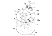
図1は、超電導磁石30の全体構成を示す斜視図であり、図2は、図1のA−A線断面図である。
【0032】
これらの図に示すように、円筒形の真空容器19内に冷却用容器として円筒形の冷媒容器5が設けられ、この冷媒容器5内に4体の超電導コイル4a,4b,4c,4dが収納されている。なお、真空容器19には電流導入用電流リード11が接続されており、また第1、第2の輻射シールド17,18を冷却する小型ヘリウム冷凍機12、および注入口とヘリウムガス放出口とを有するサービスポート14が設けられている。
【0033】
各超電導コイル4a,4b,4c,4dは円形コイルとして構成されており、冷媒容器5内の平面上の4つの象限にそれぞれ配置され、液体冷媒中に浸漬されている。そして、各超電導コイル4a,4b,4c,4dは、冷媒容器5の軸心を介して対向する方向に沿って1対ずつ互いに向き合う配置とされ、これらの超電導コイル4a,4b,4c,4dが発生する磁場の方向が、後述する引上げ炉の引上げ方向に対して横方向であり、かつこれらの超電導コイル4a,4b,4c,4dの相互に隣接する1対ずつのもの同士が冷媒容器5の内側に向く配設角度(θ)100°〜130°の範囲で任意に設定できるように構成されている。
【0034】
また、超電導コイル4a,4b,4c,4dの互いに対向するもの同士の離間距離lは、真空容器19のボア寸法Dに対して1.1〜1.25倍に設定されるとともに、これらの超電導コイル4a,4b,4c,4dのコイル直径dは、ボア寸法Dに対して0.35〜0.55倍に設定されている。
【0035】
図3は、超電導磁石30を図1のB−B線縦断面図として示すとともに、この超電導磁石30を引上げ炉1の外周側に同軸的に組立てた単結晶引上げ装置を示す図である。なお、この図3に示した単結晶引上げ装置の全体構成は図18に示した従来例の構成と略同様であるから、図18との同一構成部分には同一符号を付して重複する説明は省略するが、本実施形態の単結晶引上げ装置では、半導体材料6を収容する坩堝2の周囲から4体の超電導コイル4a,4b,4c,4dにより磁場が横方向で交差する2方向で与えられる。
【0036】
図4〜図9は、以上の構成により形成される本実施形態の磁場分布例を示し、図10および図11は、本実施形態に対する比較例としての磁場分布の例を示している。
【0037】
即ち、図4は最も磁場均一性が良好となる本実施形態の最適例を示したものであり、超電導コイル4a,4b,4c,4dの配設角度θを113°とした場合の磁場分布を示している。この図4に斜線で示したように、中心磁場が略菱形でX,Y方向ともに、均一な幅広い範囲を占めている。このような磁場を図3に示したように溶融した半導体材料6に与えた場合には、その溶融液の対流、特に坩堝中心部位での対流抑止効果が極めて高くなり、上方に引上げられる単結晶体9は全体的に均一となり、従来例では単結晶体9の周縁部分に発生していたような欠陥部分が全く見られない。
【0038】
図5〜図9には、順次に、上記の超電導コイル4a,4b,4c,4dの配設角度θを100°、110°、115°、120°、130°とした場合の磁場分布を示している。これらの図示した磁場分布においても、中心磁場が十分に広い領域に亘って均一に配置されている。なお、図5および図6のように配設角度θが小さい範囲では中心磁場がX方向に若干長く現われ、逆に図7〜図9のように配設角度θが大きくなると中心磁場がY方向に若干長く現われるようになる。
【0039】
これに対し、図10に示したように、配設角度θが90°と小さい比較例の場合には、中心磁場のY方向の幅が極端に狭くなり、また図11に示したように、配設角度θが140°と大きい比較例の場合には、中心磁場のX方向の幅が極端に狭くなる。
【0040】
以上のように、本実施形態の超電導磁石30においては、円形のコイル2個1対を互いに向き合わせて2対、同一容器内に配置し、配設角度θを100°〜130°の範囲に設定したことで、ボア内部に同心円状もしくは正方傾斜状の等分布磁場を得ることができる。
【0041】
また、ボア寸法Dに対し、対向するコイル間距離lを1.1〜1.25倍の範囲に設定した場合、およびコイル直径dを0.35〜0.55倍に設定した場合には、図4〜図9に示した磁場分布の傾向がさらに確実となる。したがって、これらの要素を配設角度θとともに加味した設定とすることにより、さらに均一性のよい磁場分布を得ることができる。
【0042】
そして、単結晶引上げを行う場合には、半導体用単結晶材料6を溶融させる坩堝2を引上げ炉1に内蔵しておき、引上げ炉1の外部に配設した超電導コイル4への通電により単結晶に磁場を印加して、溶融した単結晶材料6の坩堝2内での対流を抑制しつつ単結晶を引上げる。すなわち、超電導コイル4を4以上とし、引上げ炉1の周囲に同軸的に設けた筒形容器としての真空容器19内の平面上に配置するとともに、その配置された各超電導コイル4を真空容器19の軸心を介して対向する向きに設定し、かつ超電導コイル4の相互に隣接する1対ずつのもの、すなわち超電導コイル4a,4d同士、および超電導コイル4b,4c同士が真空容器19の内側に向く配設角度θをそれぞれ100゜〜130゜の範囲に設定して半導体用単結晶を引上げる。これにより、高品質の単結晶体を歩留りよく引上げることができる。
【0043】
この単結晶引上げの際には、超電導コイル4の対向するもの同士の離間距離lを、真空容器19のボア寸法Dに対して1.1〜1.25倍に設定することにより、特に高品質の単結晶体を歩留りよく引上げることができる。
【0044】
図12は、円筒冷媒容器5内に収納される超電導コイル4を6個(4a,4b,4c,4d,4e,4f)とした実施形態を示している。この場合の配設角度θ等の設定は図2の場合と同様である。図13は、この場合における磁場分布図である。この図13に示したように、超電導コイル数を増大した場合には、中心磁場がさらに安定した広がりとなる。このように、コイル数を6以上の偶数個に設定することにより、さらに均一性を高めることができる。また、平面上の磁場の窪みを最小限に抑えることができる。
【0045】
図14は、円筒冷媒容器5内に収納された超電導コイル4の形状を単結晶体引上げ方向8と同一方向、即ち縦方向に長いレーストラック型、楕円型または矩形型とし、その超電導コイル4を2個1対として、互いに向き合わせて2対配置し、超電導コイル4が発生する磁場の方向が引上げ炉1の引上げ方向8に対して横方向になるように構成したものである。
【0046】
このような構成とした場合には、坩堝2内の半導体材料6の深さ方向の寸法が真円の場合に比して大となるので、磁場領域の縦方向の均一性を高めることができる。したがって、前記各手段との組合せにより、さらに磁場均一性が向上する。
【0047】
図15は、本発明に係る超電導磁石30の異なる実施形態を示す縦断面図である。この実施形態が上述した実施形態と異なる点は、図1に示した冷凍機補給口のあるサービスポート14を削除したことである。その他の構成については、図1のものと同様の構成となっている。
【0048】
この図15に示した実施形態においては、冷媒と冷媒を収納する冷媒容器を有しておらず、また、超電導コイル4は小型ヘリウム冷凍機12によって冷却されている。また、超電導コイル4は輻射シールド17で覆われており、これらは真空容器19内に収納されている。そして、電流リード11は超電導コイル4に電流を供給するようになっている。
【0049】
このような実施形態によれば、超電導コイル4が冷凍機12によって冷却され、超電導状態を保持することができるので、液体ヘリウムなどの冷却媒体を必要とせず、かつ冷媒補給に要するコストを削減することができる。
【0050】
また、図16は、小型冷媒容器22と超電導コイル4とを接続した構成のものであり、その他については、図15と略同様の構成となっている。
【0051】
この図16に示した実施形態においては、超電導コイル4が小型ヘリウム冷凍機12および小型冷媒容器22によって冷却されている。なお、小型冷媒容器22には、注液口23から冷媒を注液する。
【0052】
このような図16の実施形態によれば、小型ヘリウム冷凍機12が停止した場合でも、小型冷媒容器22内部に冷媒が存在しているため、超電導コイル4は超電導状態を保つことができる。
【0053】
図17は、図1に示した真空容器19の外周壁19a、上下壁19b,19c等のいずれかまたは全体を鉄系金属等の磁性体によって構成したものである。その他は、図1に示したものと同様の構成となっている。
【0054】
このような図17に示した構成によれば、真空容器19が磁性体であるため、超電導コイル4より発生する磁場を真空容器自体の磁性体によって吸収することができる。したがって、外周囲への漏れ磁場を緩和することができ、例えば周辺に計器類が存在する場合等においても安全な運用を行うことができる。
【0055】
【発明の効果】
本発明の超電導磁石によれば、ボア内部に磁場勾配の少ない均一性のよい横磁場を発生することができ、また、平面上に同心円状もしくは正方形状の磁場分布を発生することができ、不均衡電磁力を大幅に抑制することができる。また、本発明の単結晶引上げ装置によれば、引上げ方向の均一磁場領域が向上するとともに、横磁場方向の磁場がほぼ水平になり、不均衡電磁力の抑制により、高品質の単結晶の製造が実現できる。さらに、本発明の単結晶引上げ方法によれば、高品質の単結晶体を歩留りよく引上げることができる。
【図面の簡単な説明】
【図1】本発明に係る超電導磁石の実施形態を一部概略的に示す傾斜図。
【図2】図1のA−A線断面図。
【図3】図1のB−B線断面図であり単結晶引上げ装置全体を示す図。
【図4】本発明の実施形態における磁場分布を示す図。
【図5】本発明の実施形態における磁場分布を示す図。
【図6】本発明の実施形態における磁場分布を示す図。
【図7】本発明の実施形態における磁場分布を示す図。
【図8】本発明の実施形態における磁場分布を示す図。
【図9】本発明の実施形態における磁場分布を示す図。
【図10】前記実施形態に対する比較例を示す図。
【図11】前記実施形態に対する比較例を示す図。
【図12】本発明に係る超電導磁石の他の実施形態を一部概略的に示す傾斜図。
【図13】図12に示した実施形態における磁場分布を示す図。
【図14】本発明に係る超電導磁石の他の実施形態を一部概略的に示す傾斜図。
【図15】本発明に係る超電導磁石の他の実施形態を一部概略的に示す傾斜図。
【図16】本発明に係る超電導磁石の他の実施形態を一部概略的に示す傾斜図。
【図17】本発明に係る超電導磁石の他の実施形態を一部概略的に示す縦断面図。
【図18】従来の超電導磁石を概略的に示す傾斜図。
【図19】従来の単結晶引上げ装置を示す縦断面図。
【図20】従来例における磁場分布を示す図。
【符号の説明】
1 引上げ炉
2 坩堝
3 ヒータ
4 超電導コイル
5 円筒型冷媒容器
6 半導体材料
7 磁力線
8 引上げ方向
9 単結晶
10 坩堝中心線
11 電流リード
12 小型ヘリウム冷凍機
13 ガス放出管
14 サービスポート
15 ボア
16 冷媒容器
17 第1の輻射シールド
18 第2の輻射シールド
19 真空容器
22 小型冷媒容器
23 注液口
30 超電導磁石
d コイル直径
D ボア寸法
l コイル間距離[0001]
TECHNICAL FIELD OF THE INVENTION
The present invention relates to a single crystal pulling apparatus used for, for example, manufacturing a single crystal, a superconducting magnet applied to the single crystal pulling apparatus, and a single crystal pulling method.
[0002]
[Prior art]
Semiconductors such as silicon and gallium arsenide are composed of single crystals and are used for small to large computer memories and the like, and large capacity, low cost and high quality storage devices are required.
[0003]
Conventionally, as one of single crystal pulling methods for manufacturing a single crystal satisfying the requirements of these semiconductors, a magnetic field is applied to a semiconductor material in a molten state contained in a crucible, thereby generating a molten liquid. 2. Description of the Related Art A method of suppressing heat convection and manufacturing a large-diameter and high-quality semiconductor (generally called a Czochralski (CZ) method) is known (see
[0004]
An example of a conventional single crystal pulling apparatus using the CZ method will be described with reference to FIG. This single crystal pulling apparatus includes a pulling
[0005]
In manufacturing a single crystal, the
[0006]
Therefore, as a countermeasure, the
[0007]
Next, an example of the
[0008]
The
[0009]
[Patent Document 1]
JP 2000-114028 A
[Patent Document 2]
JP 10-139599 A
[Patent Document 3]
Japanese Patent Application Laid-Open No. H11-176630
[Patent Document 4]
JP-A-11-199367
[Problems to be solved by the invention]
FIG. 20 shows a magnetic field distribution of the
[0014]
That is, as shown by the oblique lines in FIG. 20, in the region near the central magnetic field, the uniformity of the magnetic field is not good (in the form of an elongated cross in the vertical and horizontal directions). Unable to pull quality single crystal.
[0015]
The present invention has been made in view of such circumstances, and has as its object to provide a superconducting magnet that has a small magnetic field gradient inside a bore and can generate a highly uniform transverse magnetic field.
[0016]
Another object of the present invention is to provide a single crystal pulling apparatus capable of pulling a high-quality single crystal body with good yield by using a superconducting magnet for generating a high uniform magnetic field.
[0017]
Still another object of the present invention is to provide a single crystal pulling method capable of pulling a high-quality single crystal with good yield using a superconducting magnet.
[0018]
[Means for Solving the Problems]
In order to achieve the above object, in the invention according to
[0019]
In the invention according to
[0020]
According to a third aspect of the present invention, there is provided the single crystal pulling apparatus according to the first aspect, wherein a coil diameter d of the superconducting coil is set to be 0.35 to 0.55 times the bore dimension D. I do.
[0021]
According to a fourth aspect of the present invention, there is provided a superconducting magnet having a superconducting coil built in a cylindrical cooling container, wherein the superconducting coil is disposed on a plane in the cooling container and each of the superconducting coils disposed therein is disposed on a plane. The coils are set so as to face each other with the axis of the cooling vessel interposed therebetween, and the arrangement angle θ at which the pair of superconducting coils adjacent to each other faces the inside of the cooling vessel is 100 °. Provided is a superconducting magnet characterized in that the angle is set in the range of ~ 130 °.
[0022]
In the invention according to
[0023]
According to a sixth aspect of the present invention, there is provided the superconducting magnet according to the fourth aspect, wherein a coil diameter d of the superconducting coil is set to be 0.35 to 0.55 times the bore dimension D.
[0024]
According to a seventh aspect of the present invention, there is provided the superconducting magnet according to the fourth aspect, wherein the superconducting coil is configured by an even number of four or more coils.
[0025]
According to an eighth aspect of the present invention, there is provided the superconducting magnet according to the fourth aspect, wherein the shape of the superconducting coil is a racetrack type, an elliptical shape, or a rectangular shape that is long in the axial direction of the cooling container.
[0026]
According to the ninth aspect of the present invention, the cooling means for the superconducting coil includes immersing the coil in a liquid refrigerant contained in a refrigerant container, connecting the coil to a low-temperature part of a refrigerator, or connecting the liquid to the coil. 5. A superconducting magnet according to
[0027]
According to a tenth aspect of the present invention, there is provided the superconducting magnet according to the fourth aspect, wherein a wall of a container arranged on an outer peripheral side of the superconducting coil is formed of a magnetic material.
[0028]
In the invention according to
[0029]
In the twelfth aspect of the present invention, the distance l between the opposing superconducting coils is set to be 1.1 to 1.25 times the bore size D of the cylindrical container. 11. A method for pulling a single crystal according to
[0030]
BEST MODE FOR CARRYING OUT THE INVENTION
Hereinafter, embodiments of the present invention will be described with reference to FIGS.
[0031]
FIG. 1 is a perspective view showing the entire configuration of the
[0032]
As shown in these figures, a cylindrical
[0033]
Each
[0034]
The distance l between the opposing
[0035]
FIG. 3 is a diagram showing a
[0036]
4 to 9 show examples of the magnetic field distribution of the present embodiment formed by the above configuration, and FIGS. 10 and 11 show examples of the magnetic field distribution as a comparative example with respect to the present embodiment.
[0037]
That is, FIG. 4 shows an optimal example of the present embodiment in which the magnetic field uniformity is the best, and the magnetic field distribution when the arrangement angle θ of the
[0038]
5 to 9 show magnetic field distributions when the arrangement angles θ of the
[0039]
On the other hand, as shown in FIG. 10, in the comparative example where the arrangement angle θ is as small as 90 °, the width of the center magnetic field in the Y direction becomes extremely narrow, and as shown in FIG. In the case of the comparative example in which the arrangement angle θ is as large as 140 °, the width of the central magnetic field in the X direction becomes extremely narrow.
[0040]
As described above, in the
[0041]
When the distance l between the opposed coils is set to a range of 1.1 to 1.25 times the bore size D, and when the coil diameter d is set to 0.35 to 0.55 times, The tendency of the magnetic field distribution shown in FIGS. 4 to 9 is further ensured. Therefore, by setting these elements in consideration of the arrangement angle θ, a more uniform magnetic field distribution can be obtained.
[0042]
When the single crystal is to be pulled, the
[0043]
At the time of pulling the single crystal, by setting the distance l between the opposing
[0044]
FIG. 12 shows an embodiment in which six superconducting coils 4 (4a, 4b, 4c, 4d, 4e, 4f) are accommodated in a cylindrical
[0045]
FIG. 14 shows that the shape of the
[0046]
In the case of such a configuration, the dimension in the depth direction of the
[0047]
FIG. 15 is a longitudinal sectional view showing a different embodiment of the
[0048]
In the embodiment shown in FIG. 15, there is no refrigerant and a refrigerant container for storing the refrigerant, and
[0049]
According to such an embodiment, since the
[0050]
FIG. 16 shows a configuration in which the small
[0051]
In the embodiment shown in FIG. 16,
[0052]
According to the embodiment of FIG. 16, even when the
[0053]
FIG. 17 shows that one or all of the outer
[0054]
According to the configuration shown in FIG. 17, since the
[0055]
【The invention's effect】
According to the superconducting magnet of the present invention, it is possible to generate a uniform magnetic field having a small magnetic field gradient inside the bore and a concentric or square magnetic field distribution on a plane. The balanced electromagnetic force can be greatly reduced. According to the single crystal pulling apparatus of the present invention, the uniform magnetic field region in the pulling direction is improved, and the magnetic field in the horizontal magnetic field direction is almost horizontal, and the production of high-quality single crystals is suppressed by suppressing unbalanced electromagnetic force. Can be realized. Further, according to the single crystal pulling method of the present invention, a high quality single crystal can be pulled with high yield.
[Brief description of the drawings]
FIG. 1 is a perspective view schematically showing a part of an embodiment of a superconducting magnet according to the present invention.
FIG. 2 is a sectional view taken along line AA of FIG.
FIG. 3 is a sectional view taken along line BB of FIG. 1 and shows the entire single crystal pulling apparatus.
FIG. 4 is a diagram showing a magnetic field distribution in the embodiment of the present invention.
FIG. 5 is a diagram showing a magnetic field distribution in the embodiment of the present invention.
FIG. 6 is a view showing a magnetic field distribution in the embodiment of the present invention.
FIG. 7 is a diagram showing a magnetic field distribution in the embodiment of the present invention.
FIG. 8 is a diagram showing a magnetic field distribution in the embodiment of the present invention.
FIG. 9 is a diagram showing a magnetic field distribution in the embodiment of the present invention.
FIG. 10 is a view showing a comparative example of the embodiment.
FIG. 11 is a view showing a comparative example with respect to the embodiment.
FIG. 12 is a perspective view schematically showing a part of another embodiment of the superconducting magnet according to the present invention.
FIG. 13 is a diagram showing a magnetic field distribution in the embodiment shown in FIG.
FIG. 14 is a perspective view schematically showing a part of another embodiment of the superconducting magnet according to the present invention.
FIG. 15 is a perspective view schematically showing a part of another embodiment of the superconducting magnet according to the present invention.
FIG. 16 is a perspective view schematically showing a part of another embodiment of the superconducting magnet according to the present invention.
FIG. 17 is a longitudinal sectional view schematically showing a part of another embodiment of the superconducting magnet according to the present invention.
FIG. 18 is a perspective view schematically showing a conventional superconducting magnet.
FIG. 19 is a longitudinal sectional view showing a conventional single crystal pulling apparatus.
FIG. 20 is a diagram showing a magnetic field distribution in a conventional example.
[Explanation of symbols]
DESCRIPTION OF
Claims (12)
Priority Applications (1)
| Application Number | Priority Date | Filing Date | Title |
|---|---|---|---|
| JP2003151209A JP2004051475A (en) | 2002-05-31 | 2003-05-28 | Single crystal puller, superconductive magnet, and method for pulling up single crystal |
Applications Claiming Priority (2)
| Application Number | Priority Date | Filing Date | Title |
|---|---|---|---|
| JP2002160514 | 2002-05-31 | ||
| JP2003151209A JP2004051475A (en) | 2002-05-31 | 2003-05-28 | Single crystal puller, superconductive magnet, and method for pulling up single crystal |
Publications (2)
| Publication Number | Publication Date |
|---|---|
| JP2004051475A true JP2004051475A (en) | 2004-02-19 |
| JP2004051475A5 JP2004051475A5 (en) | 2006-03-09 |
Family
ID=29727533
Family Applications (1)
| Application Number | Title | Priority Date | Filing Date |
|---|---|---|---|
| JP2003151209A Pending JP2004051475A (en) | 2002-05-31 | 2003-05-28 | Single crystal puller, superconductive magnet, and method for pulling up single crystal |
Country Status (4)
| Country | Link |
|---|---|
| US (1) | US6984264B2 (en) |
| JP (1) | JP2004051475A (en) |
| KR (1) | KR100562260B1 (en) |
| DE (1) | DE10324674B4 (en) |
Cited By (19)
| Publication number | Priority date | Publication date | Assignee | Title |
|---|---|---|---|---|
| WO2006025238A1 (en) * | 2004-09-02 | 2006-03-09 | Sumco Corporation | Magnetic field application method of pulling silicon single crystal |
| JP2007210865A (en) * | 2006-02-13 | 2007-08-23 | Sumco Corp | Silicon single crystal pulling device |
| KR100831965B1 (en) | 2007-04-13 | 2008-05-23 | 순천향대학교 산학협력단 | Low temperature container for superconductor total loss measuring device |
| WO2008146371A1 (en) | 2007-05-30 | 2008-12-04 | Sumco Corporation | Silicon single-crystal pullup apparatus |
| US7528605B2 (en) | 2006-11-17 | 2009-05-05 | Hitachi, Ltd. | Superconductive magnet device and magnetic resonance imaging apparatus |
| JP2009130081A (en) * | 2007-11-22 | 2009-06-11 | Toshiba Corp | Superconducting magnet device |
| JP2009216424A (en) * | 2008-03-07 | 2009-09-24 | Kobe Steel Ltd | Magnet position measuring method and magnetic field measuring instrument |
| WO2009145149A1 (en) | 2008-05-26 | 2009-12-03 | 株式会社東芝 | Superconducting magnet device for single crystal puller |
| JP2017057127A (en) * | 2015-09-18 | 2017-03-23 | 信越半導体株式会社 | Single crystal pulling-up device and single crystal pulling-up method |
| WO2017199536A1 (en) * | 2016-05-16 | 2017-11-23 | 信越半導体株式会社 | Single crystal pulling device and single crystal pulling method |
| WO2019184129A1 (en) * | 2018-03-30 | 2019-10-03 | 苏州八匹马超导科技有限公司 | Magnet for magnetic control of czochralski single crystals and method for magnetic control of czochralski single crystals |
| WO2020225985A1 (en) * | 2019-05-08 | 2020-11-12 | 信越半導体株式会社 | Single crystal pulling apparatus and single crystal pulling method |
| JP2021080112A (en) * | 2019-11-14 | 2021-05-27 | 信越半導体株式会社 | Apparatus and method for pulling single crystal |
| WO2022102251A1 (en) * | 2020-11-10 | 2022-05-19 | 株式会社Sumco | Single crystal production method, magnetic field generator, and single crystal production device |
| KR20220145847A (en) | 2020-03-17 | 2022-10-31 | 신에쯔 한도타이 가부시키가이샤 | Single crystal pulling apparatus and single crystal pulling method |
| KR20230133299A (en) | 2021-01-26 | 2023-09-19 | 신에쯔 한도타이 가부시키가이샤 | Single crystal pulling device and single crystal pulling method |
| DE112022000585T5 (en) | 2021-03-15 | 2023-11-02 | Shin-Etsu Handotai Co., Ltd. | SINGLE CRYSTAL PULLING APPARATUS AND METHOD FOR PULLING SINGLE CRYSTALS |
| US11978586B2 (en) | 2021-01-18 | 2024-05-07 | Sumitomo Heavy Industries, Ltd. | Superconducting magnet device |
| JP7640403B2 (en) | 2021-08-06 | 2025-03-05 | 住友重機械工業株式会社 | Superconducting magnet device |
Families Citing this family (7)
| Publication number | Priority date | Publication date | Assignee | Title |
|---|---|---|---|---|
| US7713888B2 (en) * | 2004-05-24 | 2010-05-11 | Ashkenazi Brian I | Magnetic processing of electronic materials |
| EP1930484B1 (en) * | 2005-07-13 | 2014-07-23 | Shin-Etsu Handotai Co., Ltd. | Process for producing silicon single crystal |
| KR100954291B1 (en) * | 2008-01-21 | 2010-04-26 | 주식회사 실트론 | High quality semiconductor single crystal ingot manufacturing apparatus and method |
| US20100050929A1 (en) * | 2008-08-27 | 2010-03-04 | Accel Instruments Gmbh | Coil Arrangement for Crystal Pulling and Method of Forming a Crystal |
| US9127377B2 (en) | 2012-08-21 | 2015-09-08 | Babcock Noell Gmbh | Generating a homogeneous magnetic field while pulling a single crystal from molten semiconductor material |
| FR3092655B1 (en) * | 2019-02-07 | 2021-02-12 | Inst Polytechnique Grenoble | Cold crucible |
| CN116031040B (en) * | 2023-02-24 | 2023-06-20 | 安徽联效科技有限公司 | Superconducting magnet for magnetic control Czochralski single crystal and refrigerating method |
Family Cites Families (5)
| Publication number | Priority date | Publication date | Assignee | Title |
|---|---|---|---|---|
| JP3520883B2 (en) * | 1995-12-29 | 2004-04-19 | 信越半導体株式会社 | Single crystal manufacturing method |
| JPH10130100A (en) * | 1996-10-24 | 1998-05-19 | Komatsu Electron Metals Co Ltd | Apparatus for production of semiconductor single crystal and its production |
| JP3592467B2 (en) * | 1996-11-14 | 2004-11-24 | 株式会社東芝 | Superconducting magnet for single crystal pulling device |
| WO2000055393A1 (en) * | 1999-03-17 | 2000-09-21 | Shin-Etsu Handotai Co., Ltd. | Method for producing silicon single crystal and apparatus for producing the same, and single crystal and wafer produced with the method |
| JP3609312B2 (en) | 2000-01-21 | 2005-01-12 | 住友重機械工業株式会社 | Superconducting magnet device for horizontal magnetic field generation |
-
2003
- 2003-05-28 JP JP2003151209A patent/JP2004051475A/en active Pending
- 2003-05-30 US US10/448,343 patent/US6984264B2/en not_active Expired - Lifetime
- 2003-05-30 DE DE10324674.6A patent/DE10324674B4/en not_active Expired - Lifetime
- 2003-05-30 KR KR1020030034854A patent/KR100562260B1/en active IP Right Grant
Cited By (49)
| Publication number | Priority date | Publication date | Assignee | Title |
|---|---|---|---|---|
| WO2006025238A1 (en) * | 2004-09-02 | 2006-03-09 | Sumco Corporation | Magnetic field application method of pulling silicon single crystal |
| JP2007210865A (en) * | 2006-02-13 | 2007-08-23 | Sumco Corp | Silicon single crystal pulling device |
| US7528605B2 (en) | 2006-11-17 | 2009-05-05 | Hitachi, Ltd. | Superconductive magnet device and magnetic resonance imaging apparatus |
| KR100831965B1 (en) | 2007-04-13 | 2008-05-23 | 순천향대학교 산학협력단 | Low temperature container for superconductor total loss measuring device |
| KR101000326B1 (en) * | 2007-05-30 | 2010-12-13 | 가부시키가이샤 사무코 | Silicon single crystal pulling device |
| WO2008146371A1 (en) | 2007-05-30 | 2008-12-04 | Sumco Corporation | Silicon single-crystal pullup apparatus |
| EP2022876A1 (en) * | 2007-05-30 | 2009-02-11 | SUMCO Corporation | Silicon single-crystal pullup apparatus |
| US8795432B2 (en) | 2007-05-30 | 2014-08-05 | Sumco Corporation | Apparatus for pulling silicon single crystal |
| EP2022876A4 (en) * | 2007-05-30 | 2010-05-05 | Sumco Corp | Silicon single-crystal pullup apparatus |
| JP2009130081A (en) * | 2007-11-22 | 2009-06-11 | Toshiba Corp | Superconducting magnet device |
| JP2009216424A (en) * | 2008-03-07 | 2009-09-24 | Kobe Steel Ltd | Magnet position measuring method and magnetic field measuring instrument |
| WO2009145149A1 (en) | 2008-05-26 | 2009-12-03 | 株式会社東芝 | Superconducting magnet device for single crystal puller |
| EP2287366A1 (en) * | 2008-05-26 | 2011-02-23 | Kabushiki Kaisha Toshiba | Superconducting magnet device for single crystal puller |
| US8280468B2 (en) | 2008-05-26 | 2012-10-02 | Kabushiki Kaisha Toshiba | Superconducting magnet device for single crystal pulling apparatus |
| EP2287366A4 (en) * | 2008-05-26 | 2012-11-21 | Toshiba Kk | SUPERCONDUCTING MAGNETIC DEVICE FOR SINGLE CRYSTAL DRAWING DEVICE |
| JP2010006687A (en) * | 2008-05-26 | 2010-01-14 | Toshiba Corp | Superconductive magnet device for single crystal puller |
| CN108026660B (en) * | 2015-09-18 | 2020-07-24 | 信越半导体株式会社 | Single crystal pulling device and single crystal pulling method |
| KR20210107902A (en) | 2015-09-18 | 2021-09-01 | 신에쯔 한도타이 가부시키가이샤 | Single crystal pulling device and single crystal pulling method |
| CN108026660A (en) * | 2015-09-18 | 2018-05-11 | 信越半导体株式会社 | Single crystal drawing device and crystal-pulling method |
| DE112016003796T5 (en) | 2015-09-18 | 2018-05-30 | Shin-Etsu Handotai Co., Ltd. | Apparatus for pulling a single crystal and method for pulling a single crystal |
| US10253425B2 (en) | 2015-09-18 | 2019-04-09 | Shin-Etsu Handotai Co., Ltd. | Single-crystal pulling apparatus and single-crystal pulling method |
| DE112016003796B4 (en) | 2015-09-18 | 2025-02-13 | Shin-Etsu Handotai Co., Ltd. | Apparatus for pulling a single crystal and method for pulling a single crystal |
| JP2017057127A (en) * | 2015-09-18 | 2017-03-23 | 信越半導体株式会社 | Single crystal pulling-up device and single crystal pulling-up method |
| KR102478863B1 (en) * | 2015-09-18 | 2022-12-19 | 신에쯔 한도타이 가부시키가이샤 | Single crystal pulling device and single crystal pulling method |
| WO2017047008A1 (en) * | 2015-09-18 | 2017-03-23 | 信越半導体株式会社 | Single crystal pulling device and single crystal pulling method |
| WO2017199536A1 (en) * | 2016-05-16 | 2017-11-23 | 信越半導体株式会社 | Single crystal pulling device and single crystal pulling method |
| JP2017206396A (en) * | 2016-05-16 | 2017-11-24 | 信越半導体株式会社 | Apparatus and method for pulling single crystal |
| JP7029733B2 (en) | 2018-03-30 | 2022-03-04 | 蘇州八匹馬超導科技有限公司 | A magnetic material used to raise the magnetic field application of a single crystal, and a method of raising the magnetic field application of a single crystal. |
| JP2020522457A (en) * | 2018-03-30 | 2020-07-30 | 蘇州八匹馬超導科技有限公司Suzhou Bama Superconductive Technology Co.,Ltd | Magnetic substance used for pulling single crystal magnetic field and method for pulling single crystal magnetic field |
| WO2019184129A1 (en) * | 2018-03-30 | 2019-10-03 | 苏州八匹马超导科技有限公司 | Magnet for magnetic control of czochralski single crystals and method for magnetic control of czochralski single crystals |
| JP2020183334A (en) * | 2019-05-08 | 2020-11-12 | 信越半導体株式会社 | Single crystal pulling device and single crystal pulling method |
| KR20220006513A (en) | 2019-05-08 | 2022-01-17 | 신에쯔 한도타이 가부시키가이샤 | Single crystal pulling apparatus and single crystal pulling method |
| DE112020001801T5 (en) | 2019-05-08 | 2022-01-20 | Shin-Etsu Handotai Co., Ltd. | Single crystal pulling apparatus and single crystal pulling method |
| WO2020225985A1 (en) * | 2019-05-08 | 2020-11-12 | 信越半導体株式会社 | Single crystal pulling apparatus and single crystal pulling method |
| US12227872B2 (en) | 2019-05-08 | 2025-02-18 | Shin-Etsu Handotai Co., Ltd. | Single-crystal pulling apparatus and single-crystal pulling method |
| JP2021080112A (en) * | 2019-11-14 | 2021-05-27 | 信越半導体株式会社 | Apparatus and method for pulling single crystal |
| JP7230781B2 (en) | 2019-11-14 | 2023-03-01 | 信越半導体株式会社 | Single crystal pulling apparatus and single crystal pulling method |
| US12188153B2 (en) | 2020-03-17 | 2025-01-07 | Shin-Etsu Handotai Co., Ltd. | Single-crystal pulling apparatus with saddle-shaped superconducting coils and single-crystal pulling method |
| KR20220145847A (en) | 2020-03-17 | 2022-10-31 | 신에쯔 한도타이 가부시키가이샤 | Single crystal pulling apparatus and single crystal pulling method |
| DE112021000599T5 (en) | 2020-03-17 | 2022-12-08 | Shin-Etsu Handotai Co., Ltd. | Apparatus for pulling a single crystal and method for pulling a single crystal |
| WO2022102251A1 (en) * | 2020-11-10 | 2022-05-19 | 株式会社Sumco | Single crystal production method, magnetic field generator, and single crystal production device |
| US11978586B2 (en) | 2021-01-18 | 2024-05-07 | Sumitomo Heavy Industries, Ltd. | Superconducting magnet device |
| JP7590192B2 (en) | 2021-01-18 | 2024-11-26 | 住友重機械工業株式会社 | Superconducting magnet device |
| DE112021006162T5 (en) | 2021-01-26 | 2023-09-28 | Shin-Etsu Handotai Co., Ltd. | Device for growing a single crystal and method for growing a single crystal |
| KR20230133299A (en) | 2021-01-26 | 2023-09-19 | 신에쯔 한도타이 가부시키가이샤 | Single crystal pulling device and single crystal pulling method |
| KR20230155456A (en) | 2021-03-15 | 2023-11-10 | 신에쯔 한도타이 가부시키가이샤 | Single crystal pulling device and single crystal pulling method |
| JP7548081B2 (en) | 2021-03-15 | 2024-09-10 | 信越半導体株式会社 | Single crystal pulling apparatus and method |
| DE112022000585T5 (en) | 2021-03-15 | 2023-11-02 | Shin-Etsu Handotai Co., Ltd. | SINGLE CRYSTAL PULLING APPARATUS AND METHOD FOR PULLING SINGLE CRYSTALS |
| JP7640403B2 (en) | 2021-08-06 | 2025-03-05 | 住友重機械工業株式会社 | Superconducting magnet device |
Also Published As
| Publication number | Publication date |
|---|---|
| DE10324674A1 (en) | 2004-01-15 |
| KR100562260B1 (en) | 2006-03-22 |
| DE10324674B4 (en) | 2015-09-17 |
| US6984264B2 (en) | 2006-01-10 |
| KR20030094064A (en) | 2003-12-11 |
| US20040107894A1 (en) | 2004-06-10 |
Similar Documents
| Publication | Publication Date | Title |
|---|---|---|
| JP2004051475A (en) | Single crystal puller, superconductive magnet, and method for pulling up single crystal | |
| JP6436031B2 (en) | Single crystal pulling apparatus and single crystal pulling method | |
| US11578423B2 (en) | Magnet coil for magnetic czochralski single crystal growth and magnetic czochralski single crystal growth method | |
| US9127377B2 (en) | Generating a homogeneous magnetic field while pulling a single crystal from molten semiconductor material | |
| JP2020522457A (en) | Magnetic substance used for pulling single crystal magnetic field and method for pulling single crystal magnetic field | |
| WO2020225985A1 (en) | Single crystal pulling apparatus and single crystal pulling method | |
| JPH09188590A (en) | Production of single crystal and apparatus therefor | |
| JP6620670B2 (en) | Single crystal pulling apparatus and single crystal pulling method | |
| JP3592467B2 (en) | Superconducting magnet for single crystal pulling device | |
| TWI781037B (en) | Superconducting magnet device | |
| JP7230781B2 (en) | Single crystal pulling apparatus and single crystal pulling method | |
| JP7548081B2 (en) | Single crystal pulling apparatus and method | |
| WO2024164911A1 (en) | Magnetic control coil and crystal fabrication apparatus | |
| JP2008270463A (en) | Superconductive magnet device | |
| JP7160006B2 (en) | Single crystal pulling apparatus and single crystal pulling method | |
| JPS6036392A (en) | Apparatus for pulling single crystal | |
| JP7439900B2 (en) | Single crystal pulling equipment and single crystal pulling method | |
| JP4157424B2 (en) | Refrigerator cooled superconducting magnet device | |
| KR20090039248A (en) | Magnetic field magnets for magnetic field-applied Czochralski crystal growth apparatus | |
| JPS6278184A (en) | Single crystal growth apparatus |
Legal Events
| Date | Code | Title | Description |
|---|---|---|---|
| A521 | Written amendment |
Free format text: JAPANESE INTERMEDIATE CODE: A523 Effective date: 20060116 |
|
| A621 | Written request for application examination |
Free format text: JAPANESE INTERMEDIATE CODE: A621 Effective date: 20060116 |
|
| A977 | Report on retrieval |
Free format text: JAPANESE INTERMEDIATE CODE: A971007 Effective date: 20080623 |
|
| A131 | Notification of reasons for refusal |
Free format text: JAPANESE INTERMEDIATE CODE: A131 Effective date: 20080701 |
|
| A521 | Written amendment |
Free format text: JAPANESE INTERMEDIATE CODE: A523 Effective date: 20080828 |
|
| A02 | Decision of refusal |
Free format text: JAPANESE INTERMEDIATE CODE: A02 Effective date: 20080930 |
|
| A521 | Written amendment |
Free format text: JAPANESE INTERMEDIATE CODE: A523 Effective date: 20081201 |
|
| A911 | Transfer of reconsideration by examiner before appeal (zenchi) |
Free format text: JAPANESE INTERMEDIATE CODE: A911 Effective date: 20081208 |
|
| A912 | Removal of reconsideration by examiner before appeal (zenchi) |
Free format text: JAPANESE INTERMEDIATE CODE: A912 Effective date: 20090109 |