EP3089358B1 - Detector generating a displacement signal by injection locking and injection pulling - Google Patents
Detector generating a displacement signal by injection locking and injection pulling Download PDFInfo
- Publication number
- EP3089358B1 EP3089358B1 EP16164238.4A EP16164238A EP3089358B1 EP 3089358 B1 EP3089358 B1 EP 3089358B1 EP 16164238 A EP16164238 A EP 16164238A EP 3089358 B1 EP3089358 B1 EP 3089358B1
- Authority
- EP
- European Patent Office
- Prior art keywords
- signal
- frequency
- coupled
- analog
- generate
- Prior art date
- Legal status (The legal status is an assumption and is not a legal conclusion. Google has not performed a legal analysis and makes no representation as to the accuracy of the status listed.)
- Active
Links
- 238000002347 injection Methods 0.000 title claims description 117
- 239000007924 injection Substances 0.000 title claims description 117
- 238000006073 displacement reaction Methods 0.000 title claims description 31
- 230000010355 oscillation Effects 0.000 claims description 46
- 230000010363 phase shift Effects 0.000 claims description 17
- 239000003990 capacitor Substances 0.000 claims description 13
- 230000008878 coupling Effects 0.000 claims description 11
- 238000010168 coupling process Methods 0.000 claims description 11
- 238000005859 coupling reaction Methods 0.000 claims description 11
- 238000000034 method Methods 0.000 description 12
- 230000000694 effects Effects 0.000 description 9
- 230000003247 decreasing effect Effects 0.000 description 5
- 238000001514 detection method Methods 0.000 description 4
- 238000013461 design Methods 0.000 description 2
- 238000004891 communication Methods 0.000 description 1
- 230000009931 harmful effect Effects 0.000 description 1
- 238000005259 measurement Methods 0.000 description 1
- 238000012545 processing Methods 0.000 description 1
- 239000000243 solution Substances 0.000 description 1
- 230000001960 triggered effect Effects 0.000 description 1
Images


Classifications
-
- H—ELECTRICITY
- H04—ELECTRIC COMMUNICATION TECHNIQUE
- H04B—TRANSMISSION
- H04B1/00—Details of transmission systems, not covered by a single one of groups H04B3/00 - H04B13/00; Details of transmission systems not characterised by the medium used for transmission
- H04B1/06—Receivers
- H04B1/10—Means associated with receiver for limiting or suppressing noise or interference
-
- H—ELECTRICITY
- H04—ELECTRIC COMMUNICATION TECHNIQUE
- H04B—TRANSMISSION
- H04B17/00—Monitoring; Testing
- H04B17/30—Monitoring; Testing of propagation channels
-
- G—PHYSICS
- G01—MEASURING; TESTING
- G01S—RADIO DIRECTION-FINDING; RADIO NAVIGATION; DETERMINING DISTANCE OR VELOCITY BY USE OF RADIO WAVES; LOCATING OR PRESENCE-DETECTING BY USE OF THE REFLECTION OR RERADIATION OF RADIO WAVES; ANALOGOUS ARRANGEMENTS USING OTHER WAVES
- G01S7/00—Details of systems according to groups G01S13/00, G01S15/00, G01S17/00
- G01S7/02—Details of systems according to groups G01S13/00, G01S15/00, G01S17/00 of systems according to group G01S13/00
- G01S7/35—Details of non-pulse systems
-
- G—PHYSICS
- G01—MEASURING; TESTING
- G01S—RADIO DIRECTION-FINDING; RADIO NAVIGATION; DETERMINING DISTANCE OR VELOCITY BY USE OF RADIO WAVES; LOCATING OR PRESENCE-DETECTING BY USE OF THE REFLECTION OR RERADIATION OF RADIO WAVES; ANALOGOUS ARRANGEMENTS USING OTHER WAVES
- G01S13/00—Systems using the reflection or reradiation of radio waves, e.g. radar systems; Analogous systems using reflection or reradiation of waves whose nature or wavelength is irrelevant or unspecified
- G01S13/02—Systems using reflection of radio waves, e.g. primary radar systems; Analogous systems
- G01S13/50—Systems of measurement based on relative movement of target
- G01S13/52—Discriminating between fixed and moving objects or between objects moving at different speeds
- G01S13/536—Discriminating between fixed and moving objects or between objects moving at different speeds using transmission of continuous unmodulated waves, amplitude-, frequency-, or phase-modulated waves
-
- H—ELECTRICITY
- H03—ELECTRONIC CIRCUITRY
- H03B—GENERATION OF OSCILLATIONS, DIRECTLY OR BY FREQUENCY-CHANGING, BY CIRCUITS EMPLOYING ACTIVE ELEMENTS WHICH OPERATE IN A NON-SWITCHING MANNER; GENERATION OF NOISE BY SUCH CIRCUITS
- H03B19/00—Generation of oscillations by non-regenerative frequency multiplication or division of a signal from a separate source
- H03B19/06—Generation of oscillations by non-regenerative frequency multiplication or division of a signal from a separate source by means of discharge device or semiconductor device with more than two electrodes
- H03B19/14—Generation of oscillations by non-regenerative frequency multiplication or division of a signal from a separate source by means of discharge device or semiconductor device with more than two electrodes by means of a semiconductor device
-
- H—ELECTRICITY
- H03—ELECTRONIC CIRCUITRY
- H03L—AUTOMATIC CONTROL, STARTING, SYNCHRONISATION OR STABILISATION OF GENERATORS OF ELECTRONIC OSCILLATIONS OR PULSES
- H03L7/00—Automatic control of frequency or phase; Synchronisation
- H03L7/06—Automatic control of frequency or phase; Synchronisation using a reference signal applied to a frequency- or phase-locked loop
- H03L7/08—Details of the phase-locked loop
- H03L7/0802—Details of the phase-locked loop the loop being adapted for reducing power consumption
-
- H—ELECTRICITY
- H03—ELECTRONIC CIRCUITRY
- H03L—AUTOMATIC CONTROL, STARTING, SYNCHRONISATION OR STABILISATION OF GENERATORS OF ELECTRONIC OSCILLATIONS OR PULSES
- H03L7/00—Automatic control of frequency or phase; Synchronisation
- H03L7/06—Automatic control of frequency or phase; Synchronisation using a reference signal applied to a frequency- or phase-locked loop
- H03L7/08—Details of the phase-locked loop
- H03L7/099—Details of the phase-locked loop concerning mainly the controlled oscillator of the loop
-
- H—ELECTRICITY
- H04—ELECTRIC COMMUNICATION TECHNIQUE
- H04L—TRANSMISSION OF DIGITAL INFORMATION, e.g. TELEGRAPHIC COMMUNICATION
- H04L1/00—Arrangements for detecting or preventing errors in the information received
- H04L1/004—Arrangements for detecting or preventing errors in the information received by using forward error control
- H04L1/0045—Arrangements at the receiver end
- H04L1/0052—Realisations of complexity reduction techniques, e.g. pipelining or use of look-up tables
- H04L1/0053—Realisations of complexity reduction techniques, e.g. pipelining or use of look-up tables specially adapted for power saving
-
- G—PHYSICS
- G01—MEASURING; TESTING
- G01S—RADIO DIRECTION-FINDING; RADIO NAVIGATION; DETERMINING DISTANCE OR VELOCITY BY USE OF RADIO WAVES; LOCATING OR PRESENCE-DETECTING BY USE OF THE REFLECTION OR RERADIATION OF RADIO WAVES; ANALOGOUS ARRANGEMENTS USING OTHER WAVES
- G01S7/00—Details of systems according to groups G01S13/00, G01S15/00, G01S17/00
- G01S7/02—Details of systems according to groups G01S13/00, G01S15/00, G01S17/00 of systems according to group G01S13/00
- G01S7/03—Details of HF subsystems specially adapted therefor, e.g. common to transmitter and receiver
- G01S7/034—Duplexers
-
- H—ELECTRICITY
- H03—ELECTRONIC CIRCUITRY
- H03B—GENERATION OF OSCILLATIONS, DIRECTLY OR BY FREQUENCY-CHANGING, BY CIRCUITS EMPLOYING ACTIVE ELEMENTS WHICH OPERATE IN A NON-SWITCHING MANNER; GENERATION OF NOISE BY SUCH CIRCUITS
- H03B2200/00—Indexing scheme relating to details of oscillators covered by H03B
- H03B2200/006—Functional aspects of oscillators
- H03B2200/0074—Locking of an oscillator by injecting an input signal directly into the oscillator
-
- H—ELECTRICITY
- H03—ELECTRONIC CIRCUITRY
- H03B—GENERATION OF OSCILLATIONS, DIRECTLY OR BY FREQUENCY-CHANGING, BY CIRCUITS EMPLOYING ACTIVE ELEMENTS WHICH OPERATE IN A NON-SWITCHING MANNER; GENERATION OF NOISE BY SUCH CIRCUITS
- H03B2200/00—Indexing scheme relating to details of oscillators covered by H03B
- H03B2200/006—Functional aspects of oscillators
- H03B2200/0082—Lowering the supply voltage and saving power
-
- H—ELECTRICITY
- H03—ELECTRONIC CIRCUITRY
- H03B—GENERATION OF OSCILLATIONS, DIRECTLY OR BY FREQUENCY-CHANGING, BY CIRCUITS EMPLOYING ACTIVE ELEMENTS WHICH OPERATE IN A NON-SWITCHING MANNER; GENERATION OF NOISE BY SUCH CIRCUITS
- H03B2200/00—Indexing scheme relating to details of oscillators covered by H03B
- H03B2200/006—Functional aspects of oscillators
- H03B2200/0088—Reduction of noise
Definitions
- the present invention relates to a detector, and more particularly, a detector including a frequency multiplier generating an output signal by injection pulling.
- Patent documents EP1339165 and US2006/049977 disclose transceivers comprising a frequency multiplier circuit.
- the present invention aims at providing a frequency multiplier and a detector.
- a frequency multiplier included by the claimed detector includes a first injection terminal, an output terminal, and a second injection terminal.
- the first injection terminal is used to receive a first injection signal having a first frequency.
- the output terminal is used to output an output signal.
- the second injection terminal is used to receive a second injection signal having a second frequency.
- the frequency multiplier outputs the output signal at a frequency equal to a multiple of the first frequency by injection locking, and pulls the output signal to the second frequency by injection pulling.
- the frequency multiplier can further include a resonant circuit, a resonant circuit, a first transistor, a second transistor, a third transistor and a fourth transistor in a case.
- the resonant circuit is operated at a multiple of the first frequency, and includes a capacitor, an inductor, a first terminal, and a second terminal coupled the output terminal of the frequency multiplier.
- the first transistor includes a gate terminal coupled to the first injection terminal and being used to receive a first phase portion of the first injection signal, a first terminal coupled to the first terminal of the resonant circuit, and a second terminal used to couple to a bias current source.
- the second transistor includes a gate terminal coupled to the first injection terminal and being used to receive a second phase portion of the first injection signal, a first terminal coupled to the first terminal of the resonant circuit, and a second terminal being used to couple to the bias current source.
- the third transistor includes a gate terminal coupled to the first terminal of the first transistor, a first terminal coupled to the second terminal of the resonant circuit, and a second terminal coupled to the bias current source.
- the fourth transistor includes a gate terminal coupled to the second injection terminal and being used to receive the second injection signal, a first terminal coupled to the second terminal of the resonant circuit, and a second terminal being used to couple to a current source.
- the current source and the bias current source included by the claimed frequency multiplier can be of an identical current source.
- the frequency multiplier can further include a resonant circuit, a first transistor, a second transistor, a third transistor, a fourth transistor, a fifth transistor, a sixth transistor, a second resistor, a third resistor, a first capacitor, a second capacitor, a seventh transistor and an eighth transistor in another case.
- the resonant circuit is operated at a multiple of the first frequency, and includes a first resistor, an inductor, a voltage terminal used to couple to a voltage source, a first terminal, and a second terminal.
- the first transistor includes a gate terminal coupled to the second terminal of the resonant circuit, a first terminal, and a second terminal coupled to the output terminal of the frequency multiplier.
- the second transistor includes a gate terminal coupled to the first terminal of the resonant circuit, a first terminal coupled to a ground terminal, and a second terminal configured to couple to the ground terminal.
- the third transistor includes a gate terminal coupled to the first terminal of the resonant circuit, a first terminal coupled to the second terminal of the resonant circuit, and a second terminal.
- the fourth transistor includes a gate terminal coupled to the second terminal of the resonant circuit, a first terminal coupled to the first terminal of the resonant circuit, and a second terminal.
- the fifth transistor includes a gate terminal, a first terminal coupled to the second terminal of the third transistor, and a second terminal configured to couple to the ground terminal.
- the sixth transistor includes a gate terminal, a first terminal coupled to the second terminal of the fourth transistor, and a second terminal coupled to the second terminal of the fifth transistor and used to couple to the ground terminal.
- the second resistor includes a first terminal coupled to the gate terminal of the sixth transistor, and a second terminal used to couple to a bias voltage source.
- the third resistor includes a first terminal configured to couple to the bias voltage source, and a second terminal coupled to the gate terminal of the fifth transistor.
- the first capacitor includes a first terminal coupled to the first injection terminal and used to receive a first phase portion of the first injection signal, and a second terminal coupled to the first terminal of the second resistor.
- the gate terminal of the seventh transistor is used to receive a first phase portion of the second injection signal
- the gate terminal of the eighth transistor is used to receive a second phase portion of the second injection signal
- the claimed detector includes an oscillation source, the claimed frequency multiplier, a transceiver and a demodulator.
- the oscillation source is used to generate a first injection signal having a first frequency.
- the transceiver is coupled to the output terminal and the second injection terminal of the frequency multiplier, and used to transmit the output signal, and receive a received signal having a third frequency, wherein the received signal is used to update the second injection signal.
- the demodulator is coupled to the output terminal of the frequency multiplier, and used to perform a demodulation operation so as to generate a displacement signal according to the output signal.
- the demodulator included by the claimed detector can include a frequency mixer, an amplifier, an analog-to-digital converter and a digital signal processor in a case.
- the frequency mixer is coupled to the first injection terminal and the output terminal of the frequency multiplier, and used to mix frequencies of the first injection signal and the output signal to generate an intermediate frequency signal.
- the amplifier is coupled to the frequency mixer and used to amplify the intermediate frequency signal so as to generate an analog signal.
- the analog-to-digital converter is coupled to the amplifier and used to convert the analog signal to a digital signal.
- the digital signal processor is coupled to the analog-to-digital converter and configured to demodulate the digital signal so as to generate the displacement signal.
- the phase adjustment unit is coupled to the oscillation source and used to receive the first injection signal and adjust a phase of the first injection signal so as to generate a phase shift signal.
- the second frequency mixer is coupled to the phase adjustment unit and the output terminal of the frequency multiplier, and used to mix frequencies of the phase shift signal and the output signal to generate a second intermediate frequency signal.
- the second amplifier is coupled to the second frequency mixer and used to amplify the second intermediate frequency signal to generate a second analog signal.
- the second analog-to-digital converter is coupled to the second amplifier and used to convert the second analog signal to a second digital signal.
- the digital signal processor is coupled to the first analog-to-digital converter and the second analog-to-digital converter, and used to demodulate the first digital signal and the second digital signal so as to generate the displacement signal.
- the oscillation source can be further used to generate a phase shift signal generated by adjusting a phase of the first injection signal.
- the demodulator included by the claimed detector can include a first frequency mixer, a first amplifier, a first analog-to-digital converter, a second frequency mixer, a second amplifier, a second analog-to-digital converter and digital signal processor in yet another case.
- the first frequency mixer is coupled to the first injection terminal and the output terminal of the frequency multiplier, and used to mix frequencies of the first injection signal and the output signal to generate a first intermediate frequency signal.
- the first amplifier is coupled to the first frequency mixer and used to amplify the first intermediate frequency signal so as to generate a first analog signal.
- the demodulator included by the claimed detector can include a first frequency divider, a second frequency divider, a frequency mixer, an amplifier, an analog-to-digital converter, and a digital signal processor in yet another case.
- the first frequency divider is coupled to the oscillation source and used to divide frequency of the first injection signal so as to generate a first frequency-divided signal.
- the second frequency divider is coupled to the output terminal of the frequency multiplier and used to divide frequency of the output signal so as to generate a second frequency-divided signal.
- the frequency mixer is coupled to the first frequency divider and the second frequency divider, and used to mix frequencies of the first frequency-divided signal and the second frequency-divided signal so as to generate an intermediate frequency signal.
- the demodulator included by the claimed detector can include a first frequency divider, a second frequency divider, a first frequency mixer, a first amplifier, a first analog-to-digital converter, a phase adjustment unit, a second frequency mixer, a second amplifier, a second analog-to-digital converter and a a digital signal processor in yet another case.
- the first frequency divider is coupled to the oscillation source and used to divide frequency of the first injection signal so as to generate a first frequency-divided signal.
- the second frequency divider is coupled to the output terminal of the frequency multiplier and used to divide frequency of the output signal so as to generate a second frequency-divided signal.
- the first frequency mixer is coupled to the first frequency divider and the second frequency divider, and used to mix frequencies of the first frequency-divided signal and the second frequency-divided signal so as to generate a first intermediate frequency signal.
- the first amplifier is coupled to the first frequency mixer and used to amplify the first intermediate frequency signal so as to generate a first analog signal.
- the first analog-to-digital converter is coupled to the first amplifier and used to convert the first analog signal to a first digital signal.
- the phase adjustment unit is coupled to the first frequency divider and used to receive the first frequency-divided signal and adjust a phase of the first frequency-divided signal so as to generate a phase shift signal.
- the second frequency mixer is coupled to the phase adjustment unit and the second frequency divider, and used to mix frequencies of the phase shift signal and the second frequency-divided signal so as to generate a second intermediate frequency signal.
- the second amplifier is coupled to the second frequency mixer and used to amplify the second intermediate frequency signal so as to generate a second analog signal.
- the second analog-to-digital converter is coupled to the second amplifier and used to convert the second analog signal to a second digital signal.
- the digital signal processor is coupled to the first analog-to-digital converter and the second analog-to-digital converter, and used to demodulate the first digital signal and the second digital signal so as to generate the displacement signal.
- the oscillation source included by the claimed detector can include a phase-locked loop used to improve stability of the first injection signal.
- FIG. 1 illustrates a detector 100 according to an embodiment of the present invention.
- the detector 100 includes an oscillation source 110, an antenna 120 and a demodulator 130.
- the demodulator 130 includes a delay 1301 and a frequency mixer 1302.
- the oscillation source 110 generates an output signal Vosc with a frequency fa at beginning so that the antenna 120 may transmit a detection signal S1 with the frequency fa outward.
- a reflection signal S2 is reflected back and received by the antenna 120, and an input signal Vi is generated accordingly and sent to the oscillation source 110 and the demodulator 130.
- the reflection signal S2 has a frequency (fa+fx), so the difference between the frequency (fa+fx) of the reflection signal S2 and the frequency fa of the detection signal S1 is a frequency fx.
- the input signal Vi has the frequency (fa+fx) according to the reflection signal S2.
- the frequency fx is determined by the Doppler effect.
- the frequency fx is a positive value when the detected object moves toward the detector 100, and the frequency fx is a negative value when the detected object moves away from the detector 100.
- the frequency fx is updated according to the status of displacement of the detected object.
- the demodulator 130 may perform FM demodulation so as to generate a demodulated signal Vdm, and then obtain information of the displacement of the detected object according to the demodulated signal Vdm.
- the delay 1301 and the frequency mixer 1302 are used to obtain the frequency fx bringing information of displacement of the detected object.
- the demodulated signal Vdm may be a voltage signal and processed in voltage domain. Since the demodulated signal Vdm is approximately a signal of with zero frequency, it is easily affected by flicker noise so as to decrease SNR and increase the difficulty of subsequent digital process.
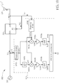
- FIG. 2 illustrates a detector 200 according to another embodiment of the present invention.
- the detector 200 includes an oscillation source 210, a frequency multiplier 220, a transceiver 230 and a demodulator 240.
- the oscillation source is used to generate an injection signal Vi1 having a frequency f1.
- the frequency multiplier 220 includes injection terminals P1 and P2, and an output terminal P3.
- the injection terminal P1 is coupled to the oscillation source 210, and used to receive the injection signal Vi1.
- the output terminal P3 is used to output an output signal Vo.
- the injection terminal P2 is used to receive an injection signal Vi2 having a frequency f2.
- the frequency multiplier 220 outputs the output signal Vo at a frequency equal to a multiple of the frequency f1 (e.g.
- the frequency multiplier 220 may be a double, triple or n-times frequency multiplier, where n is a positive integer.
- the transceiver 230 is coupled to the output terminal P3 and the injection terminal P2 of the frequency multiplier 220, and used to transmit the output signal Vo, and receive a received signal Vrx having a frequency f3. The received signal Vrx is used to update the injection signal Vi2.
- the demodulator 240 is coupled to the output terminal P3 of the frequency multiplier 220, and used to perform a demodulation operation so as to generate a displacement signal Vd according to the output signal Vo.
- the displacement signal Vd may be an analog signal or a digital signal.
- the frequency fd is a difference frequency generated by the Doppler effect.
- the difference frequency fd may be positive if the detected object is moving forward the detector 200, and the difference frequency fd may be negative if the detected object is moving away from the detector 200.
- the transceiver 230 receives the received signal Vrx having the frequency f3 (i.e. (f2+fd), for example, if fd is 100 Hz, and f2 is (10G+300) Hz, f3 is (10G+300+100) Hz, that is (10G+400) Hz)
- the received signal Vrx e.g. with a frequency of (10G+400) Hz
- the frequency of the injection signal Vi2 is be updated from the frequency f2 (e.g.
- the output signal Vo is be pulled to the frequency f3 (e.g. (10G+400) Hz) at the frequency multiplier 220 by injection pulling.
- the demodulator 240 performs demodulation operation according to the frequency f3 (i.e. f2+fd) to generate the displacement signal Vd corresponding to the difference between the frequencies f2 and f3, that is the frequency fd.
- the status of the displacement of the detected object may be determined according to the displacement signal Vd. Comparing with the oscillation source 110 operated at a high frequency (e.g.
- the operation frequency of the oscillation source 210 of the embodiment illustrated by FIG. 2 may be decreased to 50% or even lower according to the multiplier of the frequency multiplier 220, and power consumption may be effectively reduced. Furthermore, since the demodulation operation of the embodiment of the present invention is performed at an intermediate frequency instead of a zero frequency, the harmful effect of flicker noise can be better prevented as described below.
- FIG. 3 illustrates the frequency multiplier 220 according to an embodiment of the present invention.
- the frequency multiplier 220 includes a resonant circuit RC1 and transistors T1, T2, T3 and T4.
- the resonant circuit RC1 may be a tank circuit operated at a multiple (e.g. double) of the frequency f1, and includes at least a capacitor C1, at least an inductor L1, a first terminal P311, and a second terminal P312 coupled the output terminal P3 of the frequency multiplier 220.
- the inductor L1 may be coupled to a voltage source V DD according to an embodiment.
- the transistor T1 includes a gate terminal coupled to the injection terminal P1 and used to receive a first phase portion Vi11 of the injection signal Vi1, a first terminal coupled to the first terminal P311 of the resonant circuit RC1, and a second terminal coupled to a bias current source I bias .
- the transistor T2 includes a gate terminal coupled to the injection terminal P1 and used to receive a second phase portion Vi12 of the injection signal Vi1, a first terminal coupled to the first terminal P311 of the resonant circuit RC1, and a second terminal coupled to the bias current source I bias .
- a coupling unit CP1 may be disposed between the transceiver 230 and the output terminal P3 of the frequency multiplier 220, and another coupling unit CP2 may be disposed between and the transceiver 230 and the injection terminal P2 of the frequency multiplier 220.
- the coupling unit CP1/CP2 may include a power amplifier, a low noise amplifier and/or a capacitor. A designer may determine whether to dispose the coupling unit CP1 and/or the coupling unit CP2, and determine the sort of the coupling unit CP1/CP2 according to design requirement or result of measurement so as to improve the effect of detection. For example, a smaller capacitor may be chosen for signals of higher frequency.
- FIG. 5 illustrates the frequency multiplier 220 according to another embodiment of the present invention.
- the frequency multiplier 220 may include a resonant circuit RC2, transistors T11-T18, resistors R2-R3 and capacitors C11-C12.
- the resonant circuit RC2 may be operated at a multiple of the frequency f1, and includes a resistor R1, an inductor L2, a voltage terminal P513 coupled to a voltage source V DD , a first terminal P511 and a second terminal P512.
- the voltage terminal P513 may couple to the middle of the inductor L2 through the resistor R1.
- the transistor T11 may include a gate terminal coupled to the second terminal P512 of the resonant circuit RC2, a first terminal coupled to the voltage source V DD , and a second terminal coupled to the output terminal P3 of the frequency multiplier 220.
- the transistor T12 may include a gate terminal coupled to the first terminal P511 of the resonant circuit RC2, a first terminal coupled to a ground terminal, and a second terminal coupled to the ground terminal.
- the transistor T13 may include a gate terminal coupled to the first terminal P511 of the resonant circuit RC2, a first terminal coupled to the second terminal P512 of the resonant circuit RC2, and a second terminal.
- the resistor R3 may include a first terminal coupled to the bias voltage source V bias , and a second terminal coupled to the gate terminal of the transistor T15.
- the capacitor C11 may include a first terminal coupled to the injection terminal P1 and used to receive the first phase portion Vi11 of the injection signal Vi1, and a second terminal coupled to the first terminal of the resistor R1.
- the capacitor C12 may include a first terminal coupled to the injection terminal P1 and used to receive the second phase portion Vi12 of the injection signal Vi1, and a second terminal coupled to the gate terminal of the transistor T15.
- the transistor T17 may include a first terminal coupled to the gate terminal of the transistor T12, a gate terminal coupled to the injection terminal P2 and used to receive the injection signal Vi2, and a second terminal coupled to a current source Iz.
- the transistor T18 includes a first terminal coupled to the gate terminal of the transistor T11, a gate terminal coupled to the second injection terminal P2 and configured to receive the second injection signal Vi2, and a second terminal coupled to the current source Iz.
- the current source Iz may be coupled to the ground terminal.
- the gate terminal of the transistor T17 may be used to receive a first phase portion Vi21 of the injection signal Vi2
- the gate terminal of the transistor T18 may be used to receive a second phase portion Vi22 of the injection signal Vi2.
- FIG. 6 illustrates a detector 500 according to another embodiment of the present invention.
- the detector 500 may include the oscillation source 210, the frequency multiplier 220, the transceiver 230 and a demodulator 540.
- the demodulator 540 may include a frequency mixer 5410, an amplifier 5420, an analog-to-digital converter (ADC) 5430 and a digital signal processor (DSP) 5440.
- the frequency mixer 5410 may include a mixer, be coupled to the injection terminal P1 and the output terminal P3 of the frequency multiplier 220, and be used to mix frequencies of the injection signal Vi1 and the output signal Vo to generate an intermediate frequency (IF) signal Vif.
- IF intermediate frequency
- the amplifier 5420 may include a voltage amplifier and/or a current amplifier, be coupled to the frequency mixer 5410, and used to amplify the intermediate frequency signal Vif so as to generate an analog signal Vaa.
- the analog-to-digital converter 5430 may be coupled to the amplifier 5420 and used to convert the analog signal Vaa to a digital signal Sdd.
- the digital signal processor 5440 may be coupled to the analog-to-digital converter 5430 and used to demodulate the digital signal Sdd so as to generate the displacement signal Sd.
- the digital signal processor 5440 may perform FM (frequency modulation) demodulation.
- the displacement signal Sd may correspond to the status of displacement of the detected object, and the displacement signal Sd may be a digital signal.
- the frequency f1 as 5G Hz, and the difference frequency fd generated by the Doppler effect triggered by the movement of the detected object as 150 Hz may be taken for example.
- the frequency of the input signal Vi may be (fa+fx), that is (10G+150) Hz for example, hence it is known that the frequency of the intermediate frequency signal Vif (e.g. (5G+150) Hz) may be of an intermediate frequency and with much lower frequency than the input signal Vi processed by the demodulator 130 shown in FIG. 1 .
- the frequency of the intermediate frequency signal Vif e.g. (5G+150) Hz
- the intermediate frequency signal Vif may be processed by using a digital process, and is allowed to be amplified, converted from analog to digital and processed with DSP without being FM demodulated first.
- the amplifier 5420 generating the analog signal Vaa, and the analog-to-digital converter 5430 generating the digital signal Sdd may be performed in frequency domain. Since none of the analog signal Vaa and the digital signal Sdd is an approximate zero frequency signal, the demodulator 540 is difficult to be affected by flicker noise.
- the digital signal processor 5440 generates the displacement signal Sd, the FM demodulation is performed. Comparing FIG. 6 with FIG. 1 , it is known that the frequency of the processed signal may be reduced at the front-end (e.g. the frequency mixer 5410) in the embodiment of FIG. 6 so that the intermediate frequency signal may be processed by a digital process, and the reduction of SNR caused by flicker noise may be prevented.
- FIG. 7 illustrates a detector 600 according to another embodiment of the present invention.
- a demodulator 640 of the detector 600 may include frequency mixers 6410a and 6410b, amplifiers 6420a and 6420b, analog-to-digital converters 6430a and 6430b, a phase adjustment unit 6450 and a digital signal processor 6440.
- the frequency mixer 6410a may be coupled to the injection terminal P1 and the output terminal P3 of the frequency multiplier 220, and be used to mix frequencies of the injection signal Vi1 and the output signal Vo to generate an intermediate frequency signal Vif1.
- the amplifier 6420a may be coupled to the frequency mixer 6410a and be used to amplify the intermediate frequency signal Vif1 to generate an analog signal Vaa1.
- the analog-to-digital converter 6430a may be coupled to the amplifier 6420a and be used to convert the analog signal Vaa1 to a digital signal Sdd1.
- the phase adjustment unit 6450 may be coupled to the oscillation source 210 and be used to receive the injection signal Vi1 and adjust a phase of the injection signal Vi1 (e.g. by shifting 90 degrees) so as to generate a phase shift signal Vph.
- the frequency mixer 6410b may be coupled to the phase adjustment unit 6450 and the output terminal P3 of the frequency multiplier 220, and be used to mix frequencies of the phase shift signal Vph and the output signal Vo to generate an intermediate frequency signal Vif2.
- the frequency mixer 6410a, the amplifier 6420a and the analog-to-digital converter 6430a may be used to process the I-signal
- the frequency mixer 6410b, the amplifier 6420b and the analog-to-digital converter 6430b may be used to process the Q-signal. Since the I-signal is different from the Q-signal (e.g. the I-Q signals being of a sine waveform and a cosine waveform respectively), blind zones led by standing waves may be avoided.
- the structure shown in FIG. 7 with the dual-path structure may support I-Q signals to improve a demodulation performance.
- FIG. 8 illustrates a detector 700 according to another embodiment of the present invention.
- the detector 700 may include an oscillation source 710, a frequency multiplier 220, a transceiver 230 and a demodulator 740.
- the demodulator 740 may include the frequency mixers 6410a and 6410b, the amplifiers 6420a and 6420b, the analog-to-digital converters 6430a and 6430b, and the digital signal processor 6440. Different from the demodulator 640 of FIG. 7 , the demodulator 740 may not include the phase adjustment unit 6450.
- the oscillation source 710 may output the injection signal Vil having the frequency f1 and the phase shift signal Vph generated by adjusting the phase of the injection signal Vil (e.g.
- the frequency divider 8460 may be coupled to the output terminal P3 of the frequency multiplier 220, and be used to divide frequency of the output signal Vo so as to generate a frequency-divided signal Vdv2.
- the frequency mixer 8410 may be coupled to the frequency dividers 8450 and 8460, and be used to mix frequencies of the frequency-divided signals Vdv1 and Vdv2 so as to generate an intermediate frequency signal Vif8.
- the amplifier 8420 may be coupled to the frequency mixer 8410 and be used to amplify the intermediate frequency signal Vif8 so as to generate an analog signal Vaa8.
- the analog-to-digital converter 8430 may be coupled to the amplifier 8420 and be used to convert the analog signal Vaa8 to a digital signal Sdd8.
- the digital signal processor 8440 may be coupled to the analog-to-digital converter 8430 and be used to demodulate the digital signal Sdd8 so as to generate the displacement signal Sd.
- the frequency of the intermediate frequency Vif8 may be reduced to be relatively low so as to be easily processed by a digital signal process.
- the intermediate frequency Vif8 may be processed by the amplifier 8420 and the analog-to-digital converter 8430, and then be FM demodulated when being processed by the digital signal processor 8440. Since the intermediate frequency Vif8 may not be processed approximately at a zero frequency, the detector 800 may not be affected by flicker noise easily.
- FIG. 10 illustrates a detector 900 according to another embodiment of the present invention.
- the detector 900 may include the oscillation source 210, the frequency multiplier 220, the transceiver 230 and a demodulator 940.
- the operations of the oscillation source 210, the frequency multiplier 220 and the transceiver 230 may be as described above, so are not repeated herein.
- the demodulator 940 may include the frequency dividers 8450 and 8460, frequency mixers 9410a and 9410b, amplifiers 9420a and 9420b, analog-to-digital converters 9430a and 9430b, a phase adjustment unit 9450, and a digital signal processor 9440.
- the frequency divider 8450 may be coupled to the oscillation source 210 and used to divide frequency of the injection signal Vi1 so as to generate a frequency-divided signal Vdv91.
- the frequency divider 8460 may be coupled to the output terminal P3 of the frequency multiplier 220 and used to divide frequency of the output signal Vo so as to generate a frequency-divided signal Vdv92.
- the frequency mixer 9410a may be coupled to the frequency dividers 8450 and 8460, and used to mix frequencies of the frequency-divided signals Vdv91 and Vdv92 so as to generate an intermediate frequency signal Vif91.
- the amplifier 9420a may be coupled to the frequency mixer 9410a and used to amplify the intermediate frequency signal Vif91 so as to generate an analog signal Vaa91.
- the analog-to-digital converter 9430a may be coupled to the amplifier 9420a and used to convert the analog signal Vaa91 to a digital signal Sdd91.
- the phase adjustment unit 9450 may be coupled to the frequency divider 8450 and used to receive the frequency-divided signal Vdv91 and adjust a phase of the frequency-divided signal Vdv91 so as to generate a phase shift signal Vph9.
- the frequency mixer 9410b may be coupled to the phase adjustment unit 9450 and the frequency divider 8460, and used to mix frequencies of the phase shift signal Vph9 and the frequency-divided signal Vdv92 so as to generate an intermediate frequency signal Vif92.
- the detector 900 may support dual-path signals such as I-Q signals for a better effect of the demodulation.
- FIG. 11 illustrates an oscillation source 1010 according to an embodiment of the present invention.
- the oscillation sources of the detectors mentioned above may be replaced by the oscillation source 1010.
- the oscillation source 1010 may include an oscillator 1010a and a phase-locked loop 1010b. If the oscillator 1010a is analog type, the phase-locked loop 1010b may be analog type. If the oscillator 1010a is digital type, the phase-locked loop 1010b may be digital type.
- the phase-locked loop 1010b may increase the stability of the frequency of the output signal from the oscillation source 1010 without being affected by temperature or supplied voltage. The detector may therefore be more suitable for accurate applications and communication regulations.
- the detectors disclosed by embodiments of the present invention may avoid the interference made by flicker noise so that the signal-to-noise ratio may not be reduced. Furthermore, the operation frequency of the oscillation sources used in the detectors disclosed by embodiments of the present invention may be decreased greatly, so the power consumption may be decreased. The shortcomings of low signal-to-noise ratio and high power consumption of the detectors of prior art may be effectively improved.
Landscapes
- Engineering & Computer Science (AREA)
- Radar, Positioning & Navigation (AREA)
- Remote Sensing (AREA)
- Computer Networks & Wireless Communication (AREA)
- Physics & Mathematics (AREA)
- General Physics & Mathematics (AREA)
- Signal Processing (AREA)
- Electromagnetism (AREA)
- Transceivers (AREA)
- Radar Systems Or Details Thereof (AREA)
- Circuits Of Receivers In General (AREA)
- Stabilization Of Oscillater, Synchronisation, Frequency Synthesizers (AREA)
- Measurement Of Velocity Or Position Using Acoustic Or Ultrasonic Waves (AREA)
- Transmission And Conversion Of Sensor Element Output (AREA)
Description
- The present invention relates to a detector, and more particularly, a detector including a frequency multiplier generating an output signal by injection pulling.
- In general, a detector detecting the status of displacement of an object by the Doppler effect requires a high frequency input signal from an oscillation source operated at a high frequency to update the status of displacement of the object. Since it is difficult to process a high frequency signal with a digital process, an analog process is usually used to process the signal. Therefore, the signal is affected by flicker noise easily, the signal noise ratio (SNR) is reduced seriously, and the difficulty of subsequent digital signal processing (DSP) is increased. Furthermore, since the oscillation source is operated at a high frequency (e.g. around 10GHz) which cannot be decreased, the power consumption of the oscillation source cannot be decreased easily. A solution with lower power consumption and smaller effect by flicker noise is required in this field.
- Patent documents
EP1339165 andUS2006/049977 disclose transceivers comprising a frequency multiplier circuit. - The present invention aims at providing a frequency multiplier and a detector.
- This is achieved by a detector according to the claims 1-8.
- As will be seen more clearly from the detailed description following below, a frequency multiplier included by the claimed detector includes a first injection terminal, an output terminal, and a second injection terminal. The first injection terminal is used to receive a first injection signal having a first frequency. The output terminal is used to output an output signal. The second injection terminal is used to receive a second injection signal having a second frequency. The frequency multiplier outputs the output signal at a frequency equal to a multiple of the first frequency by injection locking, and pulls the output signal to the second frequency by injection pulling.
- Expediently, the frequency multiplier can further include a resonant circuit, a resonant circuit, a first transistor, a second transistor, a third transistor and a fourth transistor in a case. The resonant circuit is operated at a multiple of the first frequency, and includes a capacitor, an inductor, a first terminal, and a second terminal coupled the output terminal of the frequency multiplier. The first transistor includes a gate terminal coupled to the first injection terminal and being used to receive a first phase portion of the first injection signal, a first terminal coupled to the first terminal of the resonant circuit, and a second terminal used to couple to a bias current source. The second transistor includes a gate terminal coupled to the first injection terminal and being used to receive a second phase portion of the first injection signal, a first terminal coupled to the first terminal of the resonant circuit, and a second terminal being used to couple to the bias current source. The third transistor includes a gate terminal coupled to the first terminal of the first transistor, a first terminal coupled to the second terminal of the resonant circuit, and a second terminal coupled to the bias current source. The fourth transistor includes a gate terminal coupled to the second injection terminal and being used to receive the second injection signal, a first terminal coupled to the second terminal of the resonant circuit, and a second terminal being used to couple to a current source.
- Favorably, the current source and the bias current source included by the claimed frequency multiplier can be of an identical current source.
- Expediently, the frequency multiplier can further include a resonant circuit, a first transistor, a second transistor, a third transistor, a fourth transistor, a fifth transistor, a sixth transistor, a second resistor, a third resistor, a first capacitor, a second capacitor, a seventh transistor and an eighth transistor in another case. The resonant circuit is operated at a multiple of the first frequency, and includes a first resistor, an inductor, a voltage terminal used to couple to a voltage source, a first terminal, and a second terminal. The first transistor includes a gate terminal coupled to the second terminal of the resonant circuit, a first terminal, and a second terminal coupled to the output terminal of the frequency multiplier. The second transistor includes a gate terminal coupled to the first terminal of the resonant circuit, a first terminal coupled to a ground terminal, and a second terminal configured to couple to the ground terminal. The third transistor includes a gate terminal coupled to the first terminal of the resonant circuit, a first terminal coupled to the second terminal of the resonant circuit, and a second terminal. The fourth transistor includes a gate terminal coupled to the second terminal of the resonant circuit, a first terminal coupled to the first terminal of the resonant circuit, and a second terminal. The fifth transistor includes a gate terminal, a first terminal coupled to the second terminal of the third transistor, and a second terminal configured to couple to the ground terminal. The sixth transistor includes a gate terminal, a first terminal coupled to the second terminal of the fourth transistor, and a second terminal coupled to the second terminal of the fifth transistor and used to couple to the ground terminal. The second resistor includes a first terminal coupled to the gate terminal of the sixth transistor, and a second terminal used to couple to a bias voltage source. The third resistor includes a first terminal configured to couple to the bias voltage source, and a second terminal coupled to the gate terminal of the fifth transistor. The first capacitor includes a first terminal coupled to the first injection terminal and used to receive a first phase portion of the first injection signal, and a second terminal coupled to the first terminal of the second resistor. The second capacitor includes a first terminal coupled to the first injection terminal and used to receive a second phase portion of the first injection signal, and a second terminal coupled to the gate terminal of the fifth transistor. The seventh transistor includes a first terminal coupled to the gate terminal of the second transistor, a gate terminal coupled to the second injection terminal and used to receive the second injection signal, and a second terminal configured to couple to a current source. The eighth transistor includes a first terminal coupled to the gate terminal of the first transistor, a gate terminal coupled to the second injection terminal and used to receive the second injection signal, and a second terminal used to couple to the current source.
- Favorably, the gate terminal of the seventh transistor is used to receive a first phase portion of the second injection signal, and the gate terminal of the eighth transistor is used to receive a second phase portion of the second injection signal.
- As will be seen more clearly from the detailed description following below, the claimed detector includes an oscillation source, the claimed frequency multiplier, a transceiver and a demodulator. The oscillation source is used to generate a first injection signal having a first frequency. The transceiver is coupled to the output terminal and the second injection terminal of the frequency multiplier, and used to transmit the output signal, and receive a received signal having a third frequency, wherein the received signal is used to update the second injection signal. The demodulator is coupled to the output terminal of the frequency multiplier, and used to perform a demodulation operation so as to generate a displacement signal according to the output signal.
- Expediently, the claimed detector can further include a coupling unit. The coupling unit is disposed between the transceiver and the output terminal of the frequency multiplier, or between the second injection terminal and the transceiver. The coupling unit includes a power amplifier, a low noise amplifier and/or a capacitor.
- Expediently, the demodulator included by the claimed detector can include a frequency mixer, an amplifier, an analog-to-digital converter and a digital signal processor in a case. The frequency mixer is coupled to the first injection terminal and the output terminal of the frequency multiplier, and used to mix frequencies of the first injection signal and the output signal to generate an intermediate frequency signal. The amplifier is coupled to the frequency mixer and used to amplify the intermediate frequency signal so as to generate an analog signal. The analog-to-digital converter is coupled to the amplifier and used to convert the analog signal to a digital signal. The digital signal processor is coupled to the analog-to-digital converter and configured to demodulate the digital signal so as to generate the displacement signal.
- Expediently, the demodulator included by the claimed detector can include a first frequency mixer, a first amplifier, a first analog-to-digital converter, a phase adjustment unit, a second frequency mixer, a second amplifier, a second analog-to-digital converter and a digital signal processor in another case. The first frequency mixer is coupled to the first injection terminal and the output terminal of the frequency multiplier, and used to mix frequencies of the first injection signal and the output signal to generate a first intermediate frequency signal. The first amplifier is coupled to the first frequency mixer and used to amplify the first intermediate frequency signal to generate a first analog signal. The first analog-to-digital converter is coupled to the first amplifier and used to convert the first analog signal to a first digital signal. The phase adjustment unit is coupled to the oscillation source and used to receive the first injection signal and adjust a phase of the first injection signal so as to generate a phase shift signal. The second frequency mixer is coupled to the phase adjustment unit and the output terminal of the frequency multiplier, and used to mix frequencies of the phase shift signal and the output signal to generate a second intermediate frequency signal. The second amplifier is coupled to the second frequency mixer and used to amplify the second intermediate frequency signal to generate a second analog signal. The second analog-to-digital converter is coupled to the second amplifier and used to convert the second analog signal to a second digital signal. The digital signal processor is coupled to the first analog-to-digital converter and the second analog-to-digital converter, and used to demodulate the first digital signal and the second digital signal so as to generate the displacement signal.
- Expediently, the oscillation source can be further used to generate a phase shift signal generated by adjusting a phase of the first injection signal. The demodulator included by the claimed detector can include a first frequency mixer, a first amplifier, a first analog-to-digital converter, a second frequency mixer, a second amplifier, a second analog-to-digital converter and digital signal processor in yet another case. The first frequency mixer is coupled to the first injection terminal and the output terminal of the frequency multiplier, and used to mix frequencies of the first injection signal and the output signal to generate a first intermediate frequency signal. The first amplifier is coupled to the first frequency mixer and used to amplify the first intermediate frequency signal so as to generate a first analog signal. The first analog-to-digital converter is coupled to the first amplifier and used to convert the first analog signal to a first digital signal. The second frequency mixer is coupled to the oscillation source and the output terminal of the frequency multiplier, and used to mix frequencies of the phase shift signal and the output signal so as to generate a second intermediate frequency signal. The second amplifier is coupled to the second frequency mixer and used to amplify the second intermediate frequency signal so as to generate a second analog signal. The second analog-to-digital converter is coupled to the second amplifier and used to convert the second analog signal to a second digital signal. The digital signal processor is coupled to the first analog-to-digital converter and the second analog-to-digital converter, and used to demodulate the first digital signal and the second digital signal so as to generate the displacement signal.
- Expediently, the demodulator included by the claimed detector can include a first frequency divider, a second frequency divider, a frequency mixer, an amplifier, an analog-to-digital converter, and a digital signal processor in yet another case. The first frequency divider is coupled to the oscillation source and used to divide frequency of the first injection signal so as to generate a first frequency-divided signal. The second frequency divider is coupled to the output terminal of the frequency multiplier and used to divide frequency of the output signal so as to generate a second frequency-divided signal. The frequency mixer is coupled to the first frequency divider and the second frequency divider, and used to mix frequencies of the first frequency-divided signal and the second frequency-divided signal so as to generate an intermediate frequency signal. The amplifier is coupled to the frequency mixer and used to amplify the intermediate frequency signal so as to generate an analog signal. The analog-to-digital converter is coupled to the amplifier and used to convert the analog signal to a digital signal. The digital signal processor is coupled to the analog-to-digital converter and used to demodulate the digital signal so as to generate the displacement signal.
- Expediently, the demodulator included by the claimed detector can include a first frequency divider, a second frequency divider, a first frequency mixer, a first amplifier, a first analog-to-digital converter, a phase adjustment unit, a second frequency mixer, a second amplifier, a second analog-to-digital converter and a a digital signal processor in yet another case. The first frequency divider is coupled to the oscillation source and used to divide frequency of the first injection signal so as to generate a first frequency-divided signal. The second frequency divider is coupled to the output terminal of the frequency multiplier and used to divide frequency of the output signal so as to generate a second frequency-divided signal. The first frequency mixer is coupled to the first frequency divider and the second frequency divider, and used to mix frequencies of the first frequency-divided signal and the second frequency-divided signal so as to generate a first intermediate frequency signal. The first amplifier is coupled to the first frequency mixer and used to amplify the first intermediate frequency signal so as to generate a first analog signal. The first analog-to-digital converter is coupled to the first amplifier and used to convert the first analog signal to a first digital signal. The phase adjustment unit is coupled to the first frequency divider and used to receive the first frequency-divided signal and adjust a phase of the first frequency-divided signal so as to generate a phase shift signal. The second frequency mixer is coupled to the phase adjustment unit and the second frequency divider, and used to mix frequencies of the phase shift signal and the second frequency-divided signal so as to generate a second intermediate frequency signal. The second amplifier is coupled to the second frequency mixer and used to amplify the second intermediate frequency signal so as to generate a second analog signal. The second analog-to-digital converter is coupled to the second amplifier and used to convert the second analog signal to a second digital signal. The digital signal processor is coupled to the first analog-to-digital converter and the second analog-to-digital converter, and used to demodulate the first digital signal and the second digital signal so as to generate the displacement signal.
- Favorably, the oscillation source included by the claimed detector can include a phase-locked loop used to improve stability of the first injection signal.
- In the following, the invention is further illustrated by way of example, taking reference to the following drawings. Thereof:
- FIG. 1
- illustrates a detector according to an embodiment of the present invention;
- FIG. 2
- illustrates a detector according to another embodiment of the present invention;
- FIG. 3
- illustrates the frequency multiplier in
FIG.2 according to an embodiment of the present invention; - FIG. 4
- illustrates that the frequency multiplier of
FIG. 3 is coupled to the oscillation source and transceiver according to an embodiment of the present invention; - FIG. 5
- illustrates the frequency multiplier in
FIG.2 according to another embodiment of the present invention; - FIG. 6
- illustrates a detector according to another embodiment of the present invention;
- FIG. 7
- illustrates a detector according to another embodiment of the present invention;
- FIG. 8
- illustrates a detector according to another embodiment of the present invention;
- FIG. 9
- illustrates a detector according to another embodiment of the present invention;
- FIG. 10
- illustrates a detector according to another embodiment of the present invention; and
- FIG. 11
- illustrates an oscillation source in
FIG.2 according to an embodiment of the present invention. - Below, exemplary embodiments will be described in detail with reference to accompanying drawings so as to be easily realized by a person having ordinary knowledge in the art. The inventive concept may be embodied in various forms without being limited to the exemplary embodiments set forth herein. Descriptions of well-known parts are omitted for clarity, and like reference numerals refer to like elements throughout.
-
FIG. 1 illustrates adetector 100 according to an embodiment of the present invention. Thedetector 100 includes anoscillation source 110, anantenna 120 and ademodulator 130. Thedemodulator 130 includes adelay 1301 and afrequency mixer 1302. Theoscillation source 110 generates an output signal Vosc with a frequency fa at beginning so that theantenna 120 may transmit a detection signal S1 with the frequency fa outward. When the detection signal S1 detects a detected object, a reflection signal S2 is reflected back and received by theantenna 120, and an input signal Vi is generated accordingly and sent to theoscillation source 110 and thedemodulator 130. The reflection signal S2 has a frequency (fa+fx), so the difference between the frequency (fa+fx) of the reflection signal S2 and the frequency fa of the detection signal S1 is a frequency fx. The input signal Vi has the frequency (fa+fx) according to the reflection signal S2. The frequency fx is determined by the Doppler effect. The frequency fx is a positive value when the detected object moves toward thedetector 100, and the frequency fx is a negative value when the detected object moves away from thedetector 100. The frequency fx is updated according to the status of displacement of the detected object. When the input signal Vi is input into thedemodulator 130, an analog process is used since the frequency (fa+fx) of the input signal Vi is high (e.g. 10 GHz ±150Hz). Thedemodulator 130 may perform FM demodulation so as to generate a demodulated signal Vdm, and then obtain information of the displacement of the detected object according to the demodulated signal Vdm. Thedelay 1301 and thefrequency mixer 1302 are used to obtain the frequency fx bringing information of displacement of the detected object. The demodulated signal Vdm may be a voltage signal and processed in voltage domain. Since the demodulated signal Vdm is approximately a signal of with zero frequency, it is easily affected by flicker noise so as to decrease SNR and increase the difficulty of subsequent digital process. -
FIG. 2 illustrates adetector 200 according to another embodiment of the present invention. Thedetector 200 includes anoscillation source 210, afrequency multiplier 220, atransceiver 230 and ademodulator 240. The oscillation source is used to generate an injection signal Vi1 having a frequency f1. Thefrequency multiplier 220 includes injection terminals P1 and P2, and an output terminal P3. The injection terminal P1 is coupled to theoscillation source 210, and used to receive the injection signal Vi1. The output terminal P3 is used to output an output signal Vo. The injection terminal P2 is used to receive an injection signal Vi2 having a frequency f2. Thefrequency multiplier 220 outputs
the output signal Vo at a frequency equal to a multiple of the frequency f1 (e.g. 2f1, 3f1, etc.) by injection locking, and pulls the output signal Vo to the frequency f2 by injection pulling. Thefrequency multiplier 220 may be a double, triple or n-times frequency multiplier, where n is a positive integer. Thetransceiver 230 is coupled to the output terminal P3 and the injection terminal P2 of thefrequency multiplier 220, and used to transmit the output signal Vo, and receive a received signal Vrx having a frequency f3. The received signal Vrx is used to update the injection signal Vi2. Thedemodulator 240 is coupled to the output terminal P3 of thefrequency multiplier 220, and used to perform a demodulation operation so as to generate a displacement signal Vd according to the output signal Vo. The displacement signal Vd may be an analog signal or a digital signal. - For example, if the injection signal Vi2 has the frequency f2 (e.g. (10G+300)Hz), the frequency of the output signal Vo is pulled from the double of the frequency f1 (e.g. 5G Hz), that is (f1×2) (e.g. 10GHz), to the frequency f2 (e.g. to (10G+300)Hz from 10G Hz) by injection pulling. The transceiver 230 (e.g. an antenna) transmits the output signal Vo having the frequency f2 (e.g. (10G+300) Hz) outward. When detecting a detected object (e.g. a vehicle), the received signal Vrx is be reflected to the
transceiver 230. The received signal Vrx has the frequency f3. The relation of the frequency f3 of the received signal Vrx and the frequency f2 of the output signal Vo may be described by following equation α:
- The frequency fd is a difference frequency generated by the Doppler effect.
- The difference frequency fd may be positive if the detected object is moving forward the
detector 200, and the difference frequency fd may be negative if the detected object is moving away from thedetector 200. After thetransceiver 230 receives the received signal Vrx having the frequency f3 (i.e. (f2+fd), for example, if fd is 100 Hz, and f2 is (10G+300) Hz, f3 is (10G+300+100) Hz, that is (10G+400) Hz), the received signal Vrx (e.g. with a frequency of (10G+400) Hz) is used to update the injection signal Vi2. Hence, the frequency of the injection signal Vi2 is be updated from the frequency f2 (e.g. (10G+300) Hz) to the frequency f3 (e.g. (10G+400) Hz). After the injection signal Vi2 is updated to the frequency f3 (e.g. (10G+400) Hz), the output signal Vo is be pulled to the frequency f3 (e.g. (10G+400) Hz) at thefrequency multiplier 220 by injection pulling. Thedemodulator 240 performs demodulation operation according to the frequency f3 (i.e. f2+fd) to generate the displacement signal Vd corresponding to the difference between the frequencies f2 and f3, that is the frequency fd. The status of the displacement of the detected object may be determined according to the displacement signal Vd. Comparing with theoscillation source 110 operated at a high frequency (e.g. 10G Hz) in the previous embodiment, the operation frequency of theoscillation source 210 of the embodiment illustrated byFIG. 2 may be decreased to 50% or even lower according to the multiplier of thefrequency multiplier 220, and power consumption may be effectively reduced. Furthermore, since the demodulation operation of the embodiment of the present invention is performed at an intermediate frequency instead of a zero frequency, the harmful effect of flicker noise can be better prevented as described below. -
FIG. 3 illustrates thefrequency multiplier 220 according to an embodiment of the present invention. Thefrequency multiplier 220 includes a resonant circuit RC1 and transistors T1, T2, T3 and T4. The resonant circuit RC1 may be a tank circuit operated at a multiple (e.g. double) of the frequency f1, and includes at least a capacitor C1, at least an inductor L1, a first terminal P311, and a second terminal P312 coupled the output terminal P3 of thefrequency multiplier 220. The inductor L1 may be coupled to a voltage source VDD according to an embodiment. The transistor T1 includes a gate terminal coupled to the injection terminal P1 and used to receive a first phase portion Vi11 of the injection signal Vi1, a first terminal coupled to the first terminal P311 of the resonant circuit RC1, and a second terminal coupled to a bias current source Ibias. The transistor T2 includes a gate terminal coupled to the injection terminal P1 and used to receive a second phase portion Vi12 of the injection signal Vi1, a first terminal coupled to the first terminal P311 of the resonant circuit RC1, and a second terminal coupled to the bias current source Ibias. The transistor T3 includes a gate terminal coupled to the first terminal P311 of the resonant circuit RC1, a first terminal coupled to the second terminal P312 of the resonant circuit RC1, and a second terminal coupled to the bias current source Ibias. The transistor T4 includes a gate terminal coupled to the injection terminal P2 and used to receive the injection signal Vi2, a first terminal coupled to the second terminal P312 of the resonant circuit RC1, and a second terminal coupled to a current source Ix. According to an embodiment of the present invention, the current source Ix and the bias current source Ibias may be of an identical current source.FIG. 3 may be one of the designs of thefrequency multiplier 220 rather than being used to limit the internal structure of thefrequency multiplier 220, and a designer may adjust the internal circuit of thefrequency multiplier 220 according to requirement of the product. -
FIG. 4 illustrates that thefrequency multiplier 220 ofFIG. 3 is coupled to theoscillation source 210 andtransceiver 230 according to an embodiment of the present invention. According toFIG. 4 , since the injection signal Vil is formed by the first phase portion Vi11 and second phase portion Vi12, the signals Vi11 and Vi12 may be input to the transistors T1 and T2 respectively. According to another embodiment, if the injection signal Vi1 is a single signal, an inverter may be coupled to the gate terminal of the transistor T2 so as to obtain a signal with a reversed phase of the injection signal Vi1. According to embodiment shown inFIG. 4 , a coupling unit CP1 may be disposed between thetransceiver 230 and the output terminal P3 of thefrequency multiplier 220, and another coupling unit CP2 may be disposed between and thetransceiver 230 and the injection terminal P2 of thefrequency multiplier 220. The coupling unit CP1/CP2 may include a power amplifier, a low noise amplifier and/or a capacitor. A designer may determine whether to dispose the coupling unit CP1 and/or the coupling unit CP2, and determine the sort of the coupling unit CP1/CP2 according to design requirement or result of measurement so as to improve the effect of detection. For example, a smaller capacitor may be chosen for signals of higher frequency. -
FIG. 5 illustrates thefrequency multiplier 220 according to another embodiment of the present invention. Thefrequency multiplier 220 may include a resonant circuit RC2, transistors T11-T18, resistors R2-R3 and capacitors C11-C12. The resonant circuit RC2 may be operated at a multiple of the frequency f1, and includes a resistor R1, an inductor L2, a voltage terminal P513 coupled to a voltage source VDD, a first terminal P511 and a second terminal P512. The voltage terminal P513 may couple to the middle of the inductor L2 through the resistor R1. The transistor T11 may include a gate terminal coupled to the second terminal P512 of the resonant circuit RC2, a first terminal coupled to the voltage source VDD, and a second terminal coupled to the output terminal P3 of thefrequency multiplier 220. The transistor T12 may include a gate terminal coupled to the first terminal P511 of the resonant circuit RC2, a first terminal coupled to a ground terminal, and a second terminal coupled to the ground terminal. The transistor T13 may include a gate terminal coupled to the first terminal P511 of the resonant circuit RC2, a first terminal coupled to the second terminal P512 of the resonant circuit RC2, and a second terminal. The transistor T14 may include a gate terminal coupled to the second terminal P512 of the resonant circuit RC2, a first terminal coupled to the first terminal P511 of the resonant circuit RC2, and a second terminal. The transistor T15 may include a gate terminal, a first terminal coupled to the second terminal of the transistor T13, and a second terminal coupled to the ground terminal. The transistor T16 may include a gate terminal, a first terminal coupled to the second terminal of the transistor T14, and a second terminal coupled to the second terminal of the transistor T15 and the ground terminal. The resistor R2 may include a first terminal coupled to the gate terminal of the transistor T16, and a second terminal coupled to a bias voltage source Vbias. The resistor R3 may include a first terminal coupled to the bias voltage source Vbias, and a second terminal coupled to the gate terminal of the transistor T15. The capacitor C11 may include a first terminal coupled to the injection terminal P1 and used to receive the first phase portion Vi11 of the injection signal Vi1, and a second terminal coupled to the first terminal of the resistor R1. The capacitor C12 may include a first terminal coupled to the injection terminal P1 and used to receive the second phase portion Vi12 of the injection signal Vi1, and a second terminal coupled to the gate terminal of the transistor T15. The transistor T17 may include a first terminal coupled to the gate terminal of the transistor T12, a gate terminal coupled to the injection terminal P2 and used to receive the injection signal Vi2, and a second terminal coupled to a current source Iz. The transistor T18 includes a first terminal coupled to the gate terminal of the transistor T11, a gate terminal coupled to the second injection terminal P2 and configured to receive the second injection signal Vi2, and a second terminal coupled to the current source Iz. The current source Iz may be coupled to the ground terminal. According to an embodiment of the present invention, the gate terminal of the transistor T17 may be used to receive a first phase portion Vi21 of the injection signal Vi2, and the gate terminal of the transistor T18 may be used to receive a second phase portion Vi22 of the injection signal Vi2. -
FIG. 6 illustrates adetector 500 according to another embodiment of the present invention. Thedetector 500 may include theoscillation source 210, thefrequency multiplier 220, thetransceiver 230 and ademodulator 540. Thedemodulator 540 may include afrequency mixer 5410, anamplifier 5420, an analog-to-digital converter (ADC) 5430 and a digital signal processor (DSP) 5440. Thefrequency mixer 5410 may include a mixer, be coupled to the injection terminal P1 and the output terminal P3 of thefrequency multiplier 220, and be used to mix frequencies of the injection signal Vi1 and the output signal Vo to generate an intermediate frequency (IF) signal Vif. Theamplifier 5420 may include a voltage amplifier and/or a current amplifier, be coupled to thefrequency mixer 5410, and used to amplify the intermediate frequency signal Vif so as to generate an analog signal Vaa. The analog-to-digital converter 5430 may be coupled to theamplifier 5420 and used to convert the analog signal Vaa to a digital signal Sdd. Thedigital signal processor 5440 may be coupled to the analog-to-digital converter 5430 and used to demodulate the digital signal Sdd so as to generate the displacement signal Sd. Thedigital signal processor 5440 may perform FM (frequency modulation) demodulation. The displacement signal Sd may correspond to the status of displacement of the detected object, and the displacement signal Sd may be a digital signal. - For example, if the
frequency multiplier 220 ofFIG. 6 is a double multiplier, the injection signal Vi1 has the frequency f1 (e.g. 5G Hz), and the output signal Vo is pulled by injection pulling so as to have a frequency as (f1x2+fd), that is twice the frequency f1 plus the difference frequency fd generated by the Doppler effect, the frequency of the intermediate frequency signal Vif outputted by thefrequency mixer 5410 may be shown as the equation β:
- The frequency f1 as 5G Hz, and the difference frequency fd generated by the Doppler effect triggered by the movement of the detected object as 150 Hz may be taken for example. Regarding the input signal Vi processed by the
demodulator 130 inFIG. 1 , the frequency of the input signal Vi may be (fa+fx), that is (10G+150) Hz for example, hence it is known that the frequency of the intermediate frequency signal Vif (e.g. (5G+150) Hz) may be of an intermediate frequency and with much lower frequency than the input signal Vi processed by thedemodulator 130 shown inFIG. 1 . Hence, in the embodiment ofFIG. 6 , the intermediate frequency signal Vif may be processed by using a digital process, and is allowed to be amplified, converted from analog to digital and processed with DSP without being FM demodulated first. Hence, theamplifier 5420 generating the analog signal Vaa, and the analog-to-digital converter 5430 generating the digital signal Sdd may be performed in frequency domain. Since none of the analog signal Vaa and the digital signal Sdd is an approximate zero frequency signal, thedemodulator 540 is difficult to be affected by flicker noise. When thedigital signal processor 5440 generates the displacement signal Sd, the FM demodulation is performed. ComparingFIG. 6 withFIG. 1 , it is known that the frequency of the processed signal may be reduced at the front-end (e.g. the frequency mixer 5410) in the embodiment ofFIG. 6 so that the intermediate frequency signal may be processed by a digital process, and the reduction of SNR caused by flicker noise may be prevented. -
FIG. 7 illustrates adetector 600 according to another embodiment of the present invention. Ademodulator 640 of thedetector 600 may includefrequency mixers amplifiers digital converters phase adjustment unit 6450 and adigital signal processor 6440. Thefrequency mixer 6410a may be coupled to the injection terminal P1 and the output terminal P3 of thefrequency multiplier 220, and be used to mix frequencies of the injection signal Vi1 and the output signal Vo to generate an intermediate frequency signal Vif1. Theamplifier 6420a may be coupled to thefrequency mixer 6410a and be used to amplify the intermediate frequency signal Vif1 to generate an analog signal Vaa1. The analog-to-digital converter 6430a may be coupled to theamplifier 6420a and be used to convert the analog signal Vaa1 to a digital signal Sdd1. Thephase adjustment unit 6450 may be coupled to theoscillation source 210 and be used to receive the injection signal Vi1 and adjust a phase of the injection signal Vi1 (e.g. by shifting 90 degrees) so as to generate a phase shift signal Vph. Thefrequency mixer 6410b may be coupled to thephase adjustment unit 6450 and the output terminal P3 of thefrequency multiplier 220, and be used to mix frequencies of the phase shift signal Vph and the output signal Vo to generate an intermediate frequency signal Vif2. Theamplifier 6420b may be coupled to thefrequency mixer 6410b and be used to amplify the intermediate frequency signal Vif2 to generate an analog signal Vaa2. The analog-to-digital converter 6430b may be coupled to theamplifier 6420b and be used to convert the analog signal Vaa2 to a digital signal Sdd2. Thedigital signal processor 6440 may be coupled to the analog-to-digital converters FIG. 7 , thedemodulator 640 with a dual-path structure may support dual-path signals such as I-Q signals. For example, thefrequency mixer 6410a, theamplifier 6420a and the analog-to-digital converter 6430a may be used to process the I-signal, and thefrequency mixer 6410b, theamplifier 6420b and the analog-to-digital converter 6430b may be used to process the Q-signal. Since the I-signal is different from the Q-signal (e.g. the I-Q signals being of a sine waveform and a cosine waveform respectively), blind zones led by standing waves may be avoided. The structure shown inFIG. 7 with the dual-path structure may support I-Q signals to improve a demodulation performance. -
FIG. 8 illustrates adetector 700 according to another embodiment of the present invention. Thedetector 700 may include anoscillation source 710, afrequency multiplier 220, atransceiver 230 and ademodulator 740. Thedemodulator 740 may include thefrequency mixers amplifiers digital converters digital signal processor 6440. Different from thedemodulator 640 ofFIG. 7 , thedemodulator 740 may not include thephase adjustment unit 6450. Theoscillation source 710 may output the injection signal Vil having the frequency f1 and the phase shift signal Vph generated by adjusting the phase of the injection signal Vil (e.g. shifting the phase of the injection signal Vil by 90 degrees). The operations of thefrequency mixers amplifiers digital converters digital signal processor 6440 may be as described inFIG. 7 , and are not repeated herein. Theoscillation source 710 providing two signals with different phases may be required in thedetector 700, and dual-path signals such as I-Q signals may be supported to improve a demodulation performance. -
FIG. 9 illustrates adetector 800 according to an embodiment of the present invention. Thedetector 800 may include theoscillation source 210, thefrequency multiplier 220, thetransceiver 230 and ademodulator 840. The operations of theoscillation source 210, thefrequency multiplier 220 and thetransceiver 230 may be as described above, and are not repeated herein. Thedemodulator 840 includesfrequency dividers frequency mixer 8410, anamplifier 8420, an analog-to-digital converter 8430 and adigital signal processor 8440. Thefrequency divider 8450 may be coupled to theoscillation source 210 and be used to divide frequency of the injection signal Vi1 so as to generate a frequency-divided signal Vdv1. Thefrequency divider 8460 may be coupled to the output terminal P3 of thefrequency multiplier 220, and be used to divide frequency of the output signal Vo so as to generate a frequency-divided signal Vdv2. Thefrequency mixer 8410 may be coupled to thefrequency dividers amplifier 8420 may be coupled to thefrequency mixer 8410 and be used to amplify the intermediate frequency signal Vif8 so as to generate an analog signal Vaa8. The analog-to-digital converter 8430 may be coupled to theamplifier 8420 and be used to convert the analog signal Vaa8 to a digital signal Sdd8. Thedigital signal processor 8440 may be coupled to the analog-to-digital converter 8430 and be used to demodulate the digital signal Sdd8 so as to generate the displacement signal Sd. - The
frequency divider 8450 may perform frequency division with a divisor X, and thefrequency divider 8460 may perform frequency division with a divisor Y. Suppose the frequency of the injection signal Vil is 5G Hz, the frequency of the output signal Vo is 10G Hz, the divisor X is 4 and the divisor Y is 9, the frequency of the intermediate frequency signal Vif8 may be described as the equation γ.
- Hence, the frequency of the intermediate frequency Vif8 may be reduced to be relatively low so as to be easily processed by a digital signal process. The intermediate frequency Vif8 may be processed by the
amplifier 8420 and the analog-to-digital converter 8430, and then be FM demodulated when being processed by thedigital signal processor 8440. Since the intermediate frequency Vif8 may not be processed approximately at a zero frequency, thedetector 800 may not be affected by flicker noise easily. -
FIG. 10 illustrates adetector 900 according to another embodiment of the present invention. Thedetector 900 may include theoscillation source 210, thefrequency multiplier 220, thetransceiver 230 and ademodulator 940. The operations of theoscillation source 210, thefrequency multiplier 220 and thetransceiver 230 may be as described above, so are not repeated herein. Thedemodulator 940 may include thefrequency dividers frequency mixers amplifiers digital converters phase adjustment unit 9450, and adigital signal processor 9440. Thefrequency divider 8450 may be coupled to theoscillation source 210 and used to divide frequency of the injection signal Vi1 so as to generate a frequency-divided signal Vdv91. Thefrequency divider 8460 may be coupled to the output terminal P3 of thefrequency multiplier 220 and used to divide frequency of the output signal Vo so as to generate a frequency-divided signal Vdv92. Thefrequency mixer 9410a may be coupled to thefrequency dividers amplifier 9420a may be coupled to thefrequency mixer 9410a and used to amplify the intermediate frequency signal Vif91 so as to generate an analog signal Vaa91. The analog-to-digital converter 9430a may be coupled to theamplifier 9420a and used to convert the analog signal Vaa91 to a digital signal Sdd91. Thephase adjustment unit 9450 may be coupled to thefrequency divider 8450 and used to receive the frequency-divided signal Vdv91 and adjust a phase of the frequency-divided signal Vdv91 so as to generate a phase shift signal Vph9. Thefrequency mixer 9410b may be coupled to thephase adjustment unit 9450 and thefrequency divider 8460, and used to mix frequencies of the phase shift signal Vph9 and the frequency-divided signal Vdv92 so as to generate an intermediate frequency signal Vif92. Theamplifier 9420b may be coupled to thefrequency mixer 9410b and used to amplify the intermediate frequency signal Vif92 so as to generate an analog signal Vaa92. The analog-to-digital converter 9430b may be coupled to theamplifier 9420b and used to convert the analog signal Vaa92 to a digital signal Sdd92. Thedigital signal processor 9440 may be coupled to the analog-to-digital converters detector 800, since thedetector 900 includes thefrequency dividers detector 900 such as the intermediate frequency signals Vif91 and Vif92 may be of relatively low frequency (e.g. 130MHz), it is easier to be processed by a digital signal process. FM demodulation may be not performed before the signals are sent to the amplifiers and analog-to-digital converters, so the effect of flicker noise may be avoided. Similar to thedetector 500, since thedetector 900 has a dual-path structure, it may support dual-path signals such as I-Q signals for a better effect of the demodulation. -
FIG. 11 illustrates anoscillation source 1010 according to an embodiment of the present invention. The oscillation sources of the detectors mentioned above may be replaced by theoscillation source 1010. Theoscillation source 1010 may include anoscillator 1010a and a phase-lockedloop 1010b. If theoscillator 1010a is analog type, the phase-lockedloop 1010b may be analog type. If theoscillator 1010a is digital type, the phase-lockedloop 1010b may be digital type. The phase-lockedloop 1010b may increase the stability of the frequency of the output signal from theoscillation source 1010 without being affected by temperature or supplied voltage. The detector may therefore be more suitable for accurate applications and communication regulations. - In summary, the detectors disclosed by embodiments of the present invention may avoid the interference made by flicker noise so that the signal-to-noise ratio may not be reduced. Furthermore, the operation frequency of the oscillation sources used in the detectors disclosed by embodiments of the present invention may be decreased greatly, so the power consumption may be decreased. The shortcomings of low signal-to-noise ratio and high power consumption of the detectors of prior art may be effectively improved.
Claims (8)
- A detector (200, 500, 600, 700, 800, 900) characterized by:an oscillation source (210, 710, 1010) configured to generate a first injection signal (Vi1) having a first frequency (fi);a frequency multiplier (220) comprising:a first injection terminal (P1) configured to receive a first injection signal (Vi1) having a first frequency (f1);an output terminal (P3) configured to output an output signal (Vo); anda second injection terminal (P2) configured to receive a second injection signal (Vi2) having a second frequency (f2);wherein the frequency multiplier (220) outputs the output signal (Vo) having an initial frequency equal to a multiple of the first frequency (f1) by injection locking, a frequency of the output signal (Vo) is updated by injection pulling to be a sum of a previous frequency of the output signal (Vo) and a difference frequency (fd), and the difference frequency (fd) is equal to a difference between the previous frequency of the output signal (Vo) and a frequency of a received signal (Vrx);a transceiver (230) coupled to the output terminal (P3) and the second injection terminal (P2) of the frequency multiplier (220), and configured to transmit the output signal (Vo), and receive the received signal (Vrx), wherein the transceiver (230) is configured to update the second injection signal (Vi2) by the received signal (Vrx); anda demodulator (240, 540, 640, 740, 840, 940) coupled to the output terminal (P3) of the frequency multiplier (220), and configured to perform a demodulation operation so as to generate a displacement signal (Vd) according to the output signal (Vo).
- The detector (200) of claim 1, further characterized by:a coupling unit (CP1, CP2) disposed between the transceiver (230) and the output terminal (P3) of the frequency multiplier (220), or between the second injection terminal (P2) and the transceiver (230);wherein the coupling unit (CP1, CP2) comprises a power amplifier, a low noise amplifier and/or a capacitor.
- The detector (500) of claim 1, characterized in that the demodulator (540) comprises:a frequency mixer (5410) coupled to the first injection terminal (P1) and the output terminal (P3) of the frequency multiplier (220), and configured to mix frequencies of the first injection signal (Vi1) and the output signal (Vo) to generate an intermediate frequency signal (Vif);an amplifier (5420) coupled to the frequency mixer (5410) and configured to amplify the intermediate frequency signal (Vif) so as to generate an analog signal (Vaa);an analog-to-digital converter (5430) coupled to the amplifier (5420) and configured to convert the analog signal (Vaa) to a digital signal (Sdd); anda digital signal processor (5440) coupled to the analog-to-digital converter (5430) and configured to demodulate the digital signal (Sdd) so as to generate the displacement signal (Sd).
- The detector (600) of claim 1, characterized in that the demodulator (640) comprises:a first frequency mixer (6410a) coupled to the first injection terminal (P1) and the output terminal (P3) of the frequency multiplier (220), and configured to mix frequencies of the first injection signal (Vi1) and the output signal (Vo) to generate a first intermediate frequency signal (Vif1);a first amplifier (6420a) coupled to the first frequency mixer (6410a) and configured to amplify the first intermediate frequency signal (Vif1) to generate a first analog signal (Vaa1);a first analog-to-digital converter (6430a) coupled to the first amplifier (6420a) and configured to convert the first analog signal (Vaa1) to a first digital signal (Sdd1);a phase adjustment unit (6450) coupled to the oscillation source (210) and configured to receive the first injection signal (Vi1) and adjust a phase of the first injection signal (Vi1) so as to generate a phase shift signal (Vph);a second frequency mixer (6410b) coupled to the phase adjustment unit (6450) and the output terminal (P3) of the frequency multiplier (220), and configured to mix frequencies of the phase shift signal (Vph) and the output signal (Vo) to generate a second intermediate frequency signal (Vif2);a second amplifier (6420b) coupled to the second frequency mixer (6410b) and configured to amplify the second intermediate frequency signal (Vif2) to generate a second analog signal (Vaa2);a second analog-to-digital converter (6430b) coupled to the second amplifier (6420b) and configured to convert the second analog signal (Vaa2) to a second digital signal (Sdd2); anda digital signal processor (6440) coupled to the first analog-to-digital converter (6430a) and the second analog-to-digital converter (6430b), and configured to demodulate the first digital signal (Sdd1) and the second digital signal (Sdd2) so as to generate the displacement signal (Sd).
- The detector (700) of claim 1, characterized in that the oscillation source (710) is further configured to generate a phase shift signal (Vph) generated by adjusting a phase of the first injection signal (Vi1), and the demodulator (740) comprises:a first frequency mixer (6410a) coupled to the first injection terminal (P1) and the output terminal (P3) of the frequency multiplier (220), and configured to mix frequencies of the first injection signal (Vi1) and the output signal (Vo) to generate a first intermediate frequency signal (Vif1);a first amplifier (6420a) coupled to the first frequency mixer (6410a) and configured to amplify the first intermediate frequency signal (Vif1) so as to generate a first analog signal (Vaa1);a first analog-to-digital converter (6430a) coupled to the first amplifier (6420a) and configured to convert the first analog signal (Vaa1) to a first digital signal (Sdd1);a second frequency mixer (6410b) coupled to the oscillation source (710) and the output terminal (P3) of the frequency multiplier (220), and configured to mix frequencies of the phase shift signal (Vph) and the output signal (Vo) so as to generate a second intermediate frequency signal (Vif2);a second amplifier (6420b) coupled to the second frequency mixer (6410b) and configured to amplify the second intermediate frequency signal (Vif2) so as to generate a second analog signal (Vaa2);a second analog-to-digital converter (6430b) coupled to the second amplifier (6420b) and configured to convert the second analog signal (Vaa2) to a second digital signal (Sdd2); anda digital signal processor (6440) coupled to the first analog-to-digital converter (6430a) and the second analog-to-digital converter (6430b), and configured to demodulate the first digital signal (Sdd1) and the second digital signal (Sdd2) so as to generate the displacement signal (Sd).
- The detector (800) of claim 1, characterized in that the demodulator (840) comprises:a first frequency divider (8450) coupled to the oscillation source (210) and configured to divide frequency of the first injection signal (Vi1) so as to generate a first frequency-divided signal (Vdv1);a second frequency divider (8460) coupled to the output terminal (P3) of the frequency multiplier (220) and configured to divide frequency of the output signal (Vo) so as to generate a second frequency-divided signal (Vdv2);a frequency mixer (8410) coupled to the first frequency divider (8450) and the second frequency divider (8460), and configured to mix frequencies of the first frequency-divided signal (Vdv1) and the second frequency-divided signal (Vdv2) so as to generate an intermediate frequency signal (Vif8);an amplifier (8420) coupled to the frequency mixer (8410) and configured to amplify the intermediate frequency signal (Vif8) so as to generate an analog signal (Vaa8);an analog-to-digital converter (8430) coupled to the amplifier (8420) and configured to convert the analog signal (Vaa8) to a digital signal (Sdd8); anda digital signal processor (8440) coupled to the analog-to-digital converter (8430) and configured to demodulate the digital signal (Sdd8) so as to generate the displacement signal (Sd).
- The detector (900) of claim 1, characterized in that the demodulator (940) comprises:a first frequency divider (8450) coupled to the oscillation source (210) and configured to divide frequency of the first injection signal (Vi1) so as to generate a first frequency-divided signal (Vdv91);a second frequency divider (8460) coupled to the output terminal (P3) of the frequency multiplier (220) and configured to divide frequency of the output signal (Vo) so as to generate a second frequency-divided signal (Vdv92);a first frequency mixer (9410a) coupled to the first frequency divider (8450) and the second frequency divider (8460), and configured to mix frequencies of the first frequency-divided signal (Vdv91) and the second frequency-divided signal (Vdv92) so as to generate a first intermediate frequency signal (Vif91);a first amplifier (9420a) coupled to the first frequency mixer (9410a) and configured to amplify the first intermediate frequency signal (Vif91) so as to generate a first analog signal (Vaa91);a first analog-to-digital converter (9430a) coupled to the first amplifier (9420a) and configured to convert the first analog signal (Vaa91) to a first digital signal (Sdd91);a phase adjustment unit (9450) coupled to the first frequency divider (8450) and configured to receive the first frequency-divided signal (Vdv91) and adjust a phase of the first frequency-divided signal (Vdv91) so as to generate a phase shift signal (Vph9);a second frequency mixer (9410b) coupled to the phase adjustment unit (9450) and the second frequency divider (8460), and configured to mix frequencies of the phase shift signal (Vph9) and the second frequency-divided signal (Vdv92) so as to generate a second intermediate frequency signal (Vif92);a second amplifier (9420b) coupled to the second frequency mixer (9410b) and configured to amplify the second intermediate frequency signal (Vif92) so as to generate a second analog signal (Vaa92);a second analog-to-digital converter (9430b) coupled to the second amplifier (9420b) and configured to convert the second analog signal (Vaa92) to a second digital signal (Sdd92); anda digital signal processor (9440) coupled to the first analog-to-digital converter (9430a) and the second analog-to-digital converter (9430b), and configured to demodulate the first digital signal (Sdd91) and the second digital signal (Sdd92) so as to generate the displacement signal (Sd).
- The detector (200, 500, 600, 700, 800, 900) of claim 1, characterized in that the oscillation source (210, 710, 1010) comprises a phase-locked loop (1010b) configured to improve stability of the first injection signal (Vi1).
Applications Claiming Priority (1)
| Application Number | Priority Date | Filing Date | Title |
|---|---|---|---|
| TW104111323A TWI557417B (en) | 2015-04-08 | 2015-04-08 | Detector |
Publications (3)
| Publication Number | Publication Date |
|---|---|
| EP3089358A2 EP3089358A2 (en) | 2016-11-02 |
| EP3089358A3 EP3089358A3 (en) | 2017-03-08 |
| EP3089358B1 true EP3089358B1 (en) | 2019-07-24 |
Family
ID=56092708
Family Applications (1)
| Application Number | Title | Priority Date | Filing Date |
|---|---|---|---|
| EP16164238.4A Active EP3089358B1 (en) | 2015-04-08 | 2016-04-07 | Detector generating a displacement signal by injection locking and injection pulling |
Country Status (4)
| Country | Link |
|---|---|
| US (1) | US9590671B2 (en) |
| EP (1) | EP3089358B1 (en) |
| CN (1) | CN106059690B (en) |
| TW (1) | TWI557417B (en) |
Families Citing this family (4)
| Publication number | Priority date | Publication date | Assignee | Title |
|---|---|---|---|---|
| US9885781B2 (en) * | 2015-04-08 | 2018-02-06 | Richwave Technology Corp. | Detector generating a displacement signal by injection locking and injection pulling |
| US10411716B2 (en) * | 2016-06-06 | 2019-09-10 | Richwave Technology Corp. | Subsampling motion detector for detecting motion of object under measurement |
| TWI671950B (en) * | 2017-07-07 | 2019-09-11 | 國立中山大學 | Active phase switchable array |
| US11656321B2 (en) * | 2018-07-23 | 2023-05-23 | Richwave Technology Corp. | Method of microwave motion detection with adaptive frequency control and related devices |
Family Cites Families (13)
| Publication number | Priority date | Publication date | Assignee | Title |
|---|---|---|---|---|
| US6658237B1 (en) * | 1999-03-02 | 2003-12-02 | Skyworks Solutions, Inc. | Multi-Band transceiver utilizing direct conversion receiver |
| US6360087B1 (en) * | 1999-03-02 | 2002-03-19 | Conexant Systems, Inc | Direct conversion receiver |
| US6535037B2 (en) | 2000-02-04 | 2003-03-18 | James Maligeorgos | Injection locked frequency multiplier |
| DE10206074B4 (en) * | 2002-02-13 | 2004-04-15 | Ifm Electronic Gmbh | Microwave Sensor |
| US7161527B2 (en) * | 2004-09-03 | 2007-01-09 | Honeywell International Inc. | Navigation system |
| US8238490B2 (en) * | 2009-02-25 | 2012-08-07 | Mediatek Inc. | Method and circuit for determining a Doppler shift of a signal |
| US8085088B2 (en) * | 2009-03-04 | 2011-12-27 | National Semiconductor Corporation | Quadrature signal demodulator circuitry suitable for doppler ultrasound |
| TWI493213B (en) * | 2013-01-14 | 2015-07-21 | Ind Tech Res Inst | Motion/interference signal detection system and method thereof |
| US20130058439A1 (en) * | 2011-09-06 | 2013-03-07 | Ying-Yao Lin | Receiver |
| CN103919527B (en) * | 2013-01-14 | 2017-04-12 | 财团法人工业技术研究院 | Motion/disturbance signal detection system and method |
| JP6045961B2 (en) * | 2013-01-31 | 2016-12-14 | 日本電波工業株式会社 | Crystal oscillator and oscillation device |
| US9577650B2 (en) | 2013-02-22 | 2017-02-21 | Microchip Technology Incorporated | Phase lock loop lock indicator |
| WO2015042814A1 (en) | 2013-09-25 | 2015-04-02 | Huawei Technologies Co., Ltd. | Wideband injection locked frequency multipliers, oscillators and dividers using higher order lc resonant tank |
-
2015
- 2015-04-08 TW TW104111323A patent/TWI557417B/en active
-
2016
- 2016-03-22 US US15/076,685 patent/US9590671B2/en active Active
- 2016-04-06 CN CN201610210387.2A patent/CN106059690B/en active Active
- 2016-04-07 EP EP16164238.4A patent/EP3089358B1/en active Active
Non-Patent Citations (1)
| Title |
|---|
| None * |
Also Published As
| Publication number | Publication date |
|---|---|
| US20160301433A1 (en) | 2016-10-13 |
| CN106059690B (en) | 2018-07-17 |
| EP3089358A3 (en) | 2017-03-08 |
| US9590671B2 (en) | 2017-03-07 |
| CN106059690A (en) | 2016-10-26 |
| TWI557417B (en) | 2016-11-11 |
| TW201636638A (en) | 2016-10-16 |
| EP3089358A2 (en) | 2016-11-02 |
Similar Documents
| Publication | Publication Date | Title |
|---|---|---|
| EP3089358B1 (en) | Detector generating a displacement signal by injection locking and injection pulling | |
| EP3255453B1 (en) | Subsampling motion detector for detecting motion of object under measurement | |
| US6999747B2 (en) | Passive harmonic switch mixer | |
| DK1175008T3 (en) | Frequency converter with low phase noise | |
| US8478215B2 (en) | Harmonic rejection mixer and phase adjustment method thereof | |
| US8198945B2 (en) | Quadrature oscillator with high linearity | |
| US10484214B2 (en) | Technique for crosstalk reduction | |
| CN104897938B (en) | Test and measurement instrument including asynchronous time interleaved digitizer using harmonic mixing | |
| CN107925413A (en) | Ultra-Low Phase Noise Frequency Synthesizer | |
| JP2010258516A (en) | High frequency oscillation source | |
| JP4758483B2 (en) | Electronic equipment | |
| US7373119B2 (en) | Method and apparatus for analog-to-digital conversion | |
| US9885781B2 (en) | Detector generating a displacement signal by injection locking and injection pulling | |
| KR101085693B1 (en) | Improved Broadband I / W Signal Generator | |
| NL8303754A (en) | DIRECT MIXING SYNCHRONOUS RECEIVER. | |
| JP2009525658A (en) | FM radio receiver | |
| US7277623B2 (en) | Equal duty cycle frequency divider | |
| KR101200081B1 (en) | Ultrahigh frequency I/Q sender/receiver using multi-stage harmonic mixer | |
| JP2009231883A (en) | Radio receiver | |
| KR100696411B1 (en) | Single Chip CMOS Transmitter / Receiver and How to Use It | |
| US20080048748A1 (en) | High resolution delay adjustor | |
| WO2015173306A1 (en) | Combination of local oscillator system and sub-harmonic mixer | |
| NL192945C (en) | Frequency modulation receiver. | |
| Fujimoto et al. | An application of fuzzy inference circuit for analog phase locked loop | |
| JPWO2014030350A1 (en) | Harmonic mixer circuit and control method thereof |
Legal Events
| Date | Code | Title | Description |
|---|---|---|---|
| PUAI | Public reference made under article 153(3) epc to a published international application that has entered the european phase |
Free format text: ORIGINAL CODE: 0009012 |
|
| AK | Designated contracting states |
Kind code of ref document: A2 Designated state(s): AL AT BE BG CH CY CZ DE DK EE ES FI FR GB GR HR HU IE IS IT LI LT LU LV MC MK MT NL NO PL PT RO RS SE SI SK SM TR |
|
| AX | Request for extension of the european patent |
Extension state: BA ME |
|
| PUAL | Search report despatched |
Free format text: ORIGINAL CODE: 0009013 |
|
| AK | Designated contracting states |
Kind code of ref document: A3 Designated state(s): AL AT BE BG CH CY CZ DE DK EE ES FI FR GB GR HR HU IE IS IT LI LT LU LV MC MK MT NL NO PL PT RO RS SE SI SK SM TR |
|
| AX | Request for extension of the european patent |
Extension state: BA ME |
|
| RIC1 | Information provided on ipc code assigned before grant |
Ipc: H04L 1/00 20060101ALI20170131BHEP Ipc: H03L 7/099 20060101ALI20170131BHEP Ipc: G01S 7/03 20060101ALI20170131BHEP Ipc: H03L 7/08 20060101ALI20170131BHEP Ipc: H03B 19/14 20060101AFI20170131BHEP Ipc: G01S 13/536 20060101ALI20170131BHEP Ipc: G01S 7/35 20060101ALI20170131BHEP Ipc: H04B 1/10 20060101ALI20170131BHEP |
|
| STAA | Information on the status of an ep patent application or granted ep patent |
Free format text: STATUS: REQUEST FOR EXAMINATION WAS MADE |
|
| 17P | Request for examination filed |
Effective date: 20170828 |
|
| RBV | Designated contracting states (corrected) |
Designated state(s): AL AT BE BG CH CY CZ DE DK EE ES FI FR GB GR HR HU IE IS IT LI LT LU LV MC MK MT NL NO PL PT RO RS SE SI SK SM TR |
|
| STAA | Information on the status of an ep patent application or granted ep patent |
Free format text: STATUS: EXAMINATION IS IN PROGRESS |
|
| 17Q | First examination report despatched |
Effective date: 20171024 |
|
| GRAJ | Information related to disapproval of communication of intention to grant by the applicant or resumption of examination proceedings by the epo deleted |
Free format text: ORIGINAL CODE: EPIDOSDIGR1 |
|
| STAA | Information on the status of an ep patent application or granted ep patent |
Free format text: STATUS: GRANT OF PATENT IS INTENDED |
|
| GRAP | Despatch of communication of intention to grant a patent |
Free format text: ORIGINAL CODE: EPIDOSNIGR1 |
|
| INTG | Intention to grant announced |
Effective date: 20190218 |
|
| GRAS | Grant fee paid |
Free format text: ORIGINAL CODE: EPIDOSNIGR3 |
|
| GRAA | (expected) grant |
Free format text: ORIGINAL CODE: 0009210 |
|
| STAA | Information on the status of an ep patent application or granted ep patent |
Free format text: STATUS: THE PATENT HAS BEEN GRANTED |
|
| AK | Designated contracting states |
Kind code of ref document: B1 Designated state(s): AL AT BE BG CH CY CZ DE DK EE ES FI FR GB GR HR HU IE IS IT LI LT LU LV MC MK MT NL NO PL PT RO RS SE SI SK SM TR |
|
| REG | Reference to a national code |
Ref country code: GB Ref legal event code: FG4D |
|
| REG | Reference to a national code |
Ref country code: CH Ref legal event code: EP |
|
| REG | Reference to a national code |
Ref country code: DE Ref legal event code: R096 Ref document number: 602016017181 Country of ref document: DE |
|
| REG | Reference to a national code |
Ref country code: AT Ref legal event code: REF Ref document number: 1159411 Country of ref document: AT Kind code of ref document: T Effective date: 20190815 |
|
| REG | Reference to a national code |
Ref country code: IE Ref legal event code: FG4D |
|
| REG | Reference to a national code |
Ref country code: NL Ref legal event code: MP Effective date: 20190724 |
|
| REG | Reference to a national code |
Ref country code: LT Ref legal event code: MG4D |
|
| REG | Reference to a national code |
Ref country code: DE Ref legal event code: R082 Ref document number: 602016017181 Country of ref document: DE Representative=s name: STRAUS, ALEXANDER, DIPL.-CHEM.UNIV. DR.PHIL., DE Ref country code: DE Ref legal event code: R082 Ref document number: 602016017181 Country of ref document: DE Representative=s name: 2K PATENT- UND RECHTSANWAELTE PARTNERSCHAFT MB, DE |
|
| REG | Reference to a national code |
Ref country code: AT Ref legal event code: MK05 Ref document number: 1159411 Country of ref document: AT Kind code of ref document: T Effective date: 20190724 |
|
| PG25 | Lapsed in a contracting state [announced via postgrant information from national office to epo] |
Ref country code: NO Free format text: LAPSE BECAUSE OF FAILURE TO SUBMIT A TRANSLATION OF THE DESCRIPTION OR TO PAY THE FEE WITHIN THE PRESCRIBED TIME-LIMIT Effective date: 20191024 Ref country code: AT Free format text: LAPSE BECAUSE OF FAILURE TO SUBMIT A TRANSLATION OF THE DESCRIPTION OR TO PAY THE FEE WITHIN THE PRESCRIBED TIME-LIMIT Effective date: 20190724 Ref country code: LT Free format text: LAPSE BECAUSE OF FAILURE TO SUBMIT A TRANSLATION OF THE DESCRIPTION OR TO PAY THE FEE WITHIN THE PRESCRIBED TIME-LIMIT Effective date: 20190724 Ref country code: NL Free format text: LAPSE BECAUSE OF FAILURE TO SUBMIT A TRANSLATION OF THE DESCRIPTION OR TO PAY THE FEE WITHIN THE PRESCRIBED TIME-LIMIT Effective date: 20190724 Ref country code: BG Free format text: LAPSE BECAUSE OF FAILURE TO SUBMIT A TRANSLATION OF THE DESCRIPTION OR TO PAY THE FEE WITHIN THE PRESCRIBED TIME-LIMIT Effective date: 20191024 Ref country code: PT Free format text: LAPSE BECAUSE OF FAILURE TO SUBMIT A TRANSLATION OF THE DESCRIPTION OR TO PAY THE FEE WITHIN THE PRESCRIBED TIME-LIMIT Effective date: 20191125 Ref country code: FI Free format text: LAPSE BECAUSE OF FAILURE TO SUBMIT A TRANSLATION OF THE DESCRIPTION OR TO PAY THE FEE WITHIN THE PRESCRIBED TIME-LIMIT Effective date: 20190724 Ref country code: SE Free format text: LAPSE BECAUSE OF FAILURE TO SUBMIT A TRANSLATION OF THE DESCRIPTION OR TO PAY THE FEE WITHIN THE PRESCRIBED TIME-LIMIT Effective date: 20190724 Ref country code: HR Free format text: LAPSE BECAUSE OF FAILURE TO SUBMIT A TRANSLATION OF THE DESCRIPTION OR TO PAY THE FEE WITHIN THE PRESCRIBED TIME-LIMIT Effective date: 20190724 |
|
| PG25 | Lapsed in a contracting state [announced via postgrant information from national office to epo] |
Ref country code: AL Free format text: LAPSE BECAUSE OF FAILURE TO SUBMIT A TRANSLATION OF THE DESCRIPTION OR TO PAY THE FEE WITHIN THE PRESCRIBED TIME-LIMIT Effective date: 20190724 Ref country code: GR Free format text: LAPSE BECAUSE OF FAILURE TO SUBMIT A TRANSLATION OF THE DESCRIPTION OR TO PAY THE FEE WITHIN THE PRESCRIBED TIME-LIMIT Effective date: 20191025 Ref country code: IS Free format text: LAPSE BECAUSE OF FAILURE TO SUBMIT A TRANSLATION OF THE DESCRIPTION OR TO PAY THE FEE WITHIN THE PRESCRIBED TIME-LIMIT Effective date: 20191124 Ref country code: RS Free format text: LAPSE BECAUSE OF FAILURE TO SUBMIT A TRANSLATION OF THE DESCRIPTION OR TO PAY THE FEE WITHIN THE PRESCRIBED TIME-LIMIT Effective date: 20190724 Ref country code: LV Free format text: LAPSE BECAUSE OF FAILURE TO SUBMIT A TRANSLATION OF THE DESCRIPTION OR TO PAY THE FEE WITHIN THE PRESCRIBED TIME-LIMIT Effective date: 20190724 Ref country code: ES Free format text: LAPSE BECAUSE OF FAILURE TO SUBMIT A TRANSLATION OF THE DESCRIPTION OR TO PAY THE FEE WITHIN THE PRESCRIBED TIME-LIMIT Effective date: 20190724 |
|
| PG25 | Lapsed in a contracting state [announced via postgrant information from national office to epo] |
Ref country code: TR Free format text: LAPSE BECAUSE OF FAILURE TO SUBMIT A TRANSLATION OF THE DESCRIPTION OR TO PAY THE FEE WITHIN THE PRESCRIBED TIME-LIMIT Effective date: 20190724 |
|
| PG25 | Lapsed in a contracting state [announced via postgrant information from national office to epo] |
Ref country code: IT Free format text: LAPSE BECAUSE OF FAILURE TO SUBMIT A TRANSLATION OF THE DESCRIPTION OR TO PAY THE FEE WITHIN THE PRESCRIBED TIME-LIMIT Effective date: 20190724 Ref country code: DK Free format text: LAPSE BECAUSE OF FAILURE TO SUBMIT A TRANSLATION OF THE DESCRIPTION OR TO PAY THE FEE WITHIN THE PRESCRIBED TIME-LIMIT Effective date: 20190724 Ref country code: EE Free format text: LAPSE BECAUSE OF FAILURE TO SUBMIT A TRANSLATION OF THE DESCRIPTION OR TO PAY THE FEE WITHIN THE PRESCRIBED TIME-LIMIT Effective date: 20190724 Ref country code: PL Free format text: LAPSE BECAUSE OF FAILURE TO SUBMIT A TRANSLATION OF THE DESCRIPTION OR TO PAY THE FEE WITHIN THE PRESCRIBED TIME-LIMIT Effective date: 20190724 Ref country code: RO Free format text: LAPSE BECAUSE OF FAILURE TO SUBMIT A TRANSLATION OF THE DESCRIPTION OR TO PAY THE FEE WITHIN THE PRESCRIBED TIME-LIMIT Effective date: 20190724 |
|
| PG25 | Lapsed in a contracting state [announced via postgrant information from national office to epo] |
Ref country code: CZ Free format text: LAPSE BECAUSE OF FAILURE TO SUBMIT A TRANSLATION OF THE DESCRIPTION OR TO PAY THE FEE WITHIN THE PRESCRIBED TIME-LIMIT Effective date: 20190724 Ref country code: IS Free format text: LAPSE BECAUSE OF FAILURE TO SUBMIT A TRANSLATION OF THE DESCRIPTION OR TO PAY THE FEE WITHIN THE PRESCRIBED TIME-LIMIT Effective date: 20200224 Ref country code: SM Free format text: LAPSE BECAUSE OF FAILURE TO SUBMIT A TRANSLATION OF THE DESCRIPTION OR TO PAY THE FEE WITHIN THE PRESCRIBED TIME-LIMIT Effective date: 20190724 Ref country code: SK Free format text: LAPSE BECAUSE OF FAILURE TO SUBMIT A TRANSLATION OF THE DESCRIPTION OR TO PAY THE FEE WITHIN THE PRESCRIBED TIME-LIMIT Effective date: 20190724 |
|
| REG | Reference to a national code |
Ref country code: DE Ref legal event code: R097 Ref document number: 602016017181 Country of ref document: DE |
|
| PLBE | No opposition filed within time limit |
Free format text: ORIGINAL CODE: 0009261 |
|
| STAA | Information on the status of an ep patent application or granted ep patent |
Free format text: STATUS: NO OPPOSITION FILED WITHIN TIME LIMIT |
|
| PG2D | Information on lapse in contracting state deleted |
Ref country code: IS |
|
| 26N | No opposition filed |
Effective date: 20200603 |
|
| PG25 | Lapsed in a contracting state [announced via postgrant information from national office to epo] |
Ref country code: SI Free format text: LAPSE BECAUSE OF FAILURE TO SUBMIT A TRANSLATION OF THE DESCRIPTION OR TO PAY THE FEE WITHIN THE PRESCRIBED TIME-LIMIT Effective date: 20190724 |
|
| PG25 | Lapsed in a contracting state [announced via postgrant information from national office to epo] |
Ref country code: MC Free format text: LAPSE BECAUSE OF FAILURE TO SUBMIT A TRANSLATION OF THE DESCRIPTION OR TO PAY THE FEE WITHIN THE PRESCRIBED TIME-LIMIT Effective date: 20190724 |
|
| REG | Reference to a national code |
Ref country code: CH Ref legal event code: PL |
|
| PG25 | Lapsed in a contracting state [announced via postgrant information from national office to epo] |
Ref country code: CH Free format text: LAPSE BECAUSE OF NON-PAYMENT OF DUE FEES Effective date: 20200430 Ref country code: LU Free format text: LAPSE BECAUSE OF NON-PAYMENT OF DUE FEES Effective date: 20200407 Ref country code: LI Free format text: LAPSE BECAUSE OF NON-PAYMENT OF DUE FEES Effective date: 20200430 |
|
| REG | Reference to a national code |
Ref country code: BE Ref legal event code: MM Effective date: 20200430 |
|
| PG25 | Lapsed in a contracting state [announced via postgrant information from national office to epo] |
Ref country code: BE Free format text: LAPSE BECAUSE OF NON-PAYMENT OF DUE FEES Effective date: 20200430 |
|
| PG25 | Lapsed in a contracting state [announced via postgrant information from national office to epo] |
Ref country code: IE Free format text: LAPSE BECAUSE OF NON-PAYMENT OF DUE FEES Effective date: 20200407 |
|
| PG25 | Lapsed in a contracting state [announced via postgrant information from national office to epo] |
Ref country code: MT Free format text: LAPSE BECAUSE OF FAILURE TO SUBMIT A TRANSLATION OF THE DESCRIPTION OR TO PAY THE FEE WITHIN THE PRESCRIBED TIME-LIMIT Effective date: 20190724 Ref country code: CY Free format text: LAPSE BECAUSE OF FAILURE TO SUBMIT A TRANSLATION OF THE DESCRIPTION OR TO PAY THE FEE WITHIN THE PRESCRIBED TIME-LIMIT Effective date: 20190724 |
|
| PG25 | Lapsed in a contracting state [announced via postgrant information from national office to epo] |
Ref country code: MK Free format text: LAPSE BECAUSE OF FAILURE TO SUBMIT A TRANSLATION OF THE DESCRIPTION OR TO PAY THE FEE WITHIN THE PRESCRIBED TIME-LIMIT Effective date: 20190724 |
|
| PGFP | Annual fee paid to national office [announced via postgrant information from national office to epo] |
Ref country code: DE Payment date: 20220608 Year of fee payment: 8 |
|
| PGFP | Annual fee paid to national office [announced via postgrant information from national office to epo] |
Ref country code: GB Payment date: 20240313 Year of fee payment: 9 |
|
| PGFP | Annual fee paid to national office [announced via postgrant information from national office to epo] |
Ref country code: FR Payment date: 20240313 Year of fee payment: 9 |
|
| REG | Reference to a national code |
Ref country code: DE Ref legal event code: R082 Ref document number: 602016017181 Country of ref document: DE Representative=s name: STRAUS, ALEXANDER, DIPL.-CHEM.UNIV. DR.PHIL., DE |