EP1950817A1 - Organic electroluminescent device - Google Patents
Organic electroluminescent device Download PDFInfo
- Publication number
- EP1950817A1 EP1950817A1 EP06842815A EP06842815A EP1950817A1 EP 1950817 A1 EP1950817 A1 EP 1950817A1 EP 06842815 A EP06842815 A EP 06842815A EP 06842815 A EP06842815 A EP 06842815A EP 1950817 A1 EP1950817 A1 EP 1950817A1
- Authority
- EP
- European Patent Office
- Prior art keywords
- layer
- group
- acceptor
- hole
- organic electroluminescence
- Prior art date
- Legal status (The legal status is an assumption and is not a legal conclusion. Google has not performed a legal analysis and makes no representation as to the accuracy of the status listed.)
- Withdrawn
Links
- 238000005401 electroluminescence Methods 0.000 claims abstract description 85
- 230000008021 deposition Effects 0.000 claims abstract description 6
- 150000001875 compounds Chemical class 0.000 claims description 52
- -1 phenylenediamine compound Chemical class 0.000 claims description 47
- 125000003118 aryl group Chemical group 0.000 claims description 45
- 125000000217 alkyl group Chemical group 0.000 claims description 37
- 125000004435 hydrogen atom Chemical group [H]* 0.000 claims description 30
- 239000000463 material Substances 0.000 claims description 29
- 125000000623 heterocyclic group Chemical group 0.000 claims description 28
- 125000005843 halogen group Chemical group 0.000 claims description 22
- 239000000872 buffer Substances 0.000 claims description 18
- 125000003545 alkoxy group Chemical group 0.000 claims description 14
- 125000001997 phenyl group Chemical group [H]C1=C([H])C([H])=C(*)C([H])=C1[H] 0.000 claims description 14
- 230000009467 reduction Effects 0.000 claims description 13
- 125000004093 cyano group Chemical group *C#N 0.000 claims description 12
- 125000006575 electron-withdrawing group Chemical group 0.000 claims description 12
- 125000003709 fluoroalkyl group Chemical group 0.000 claims description 12
- 125000001624 naphthyl group Chemical group 0.000 claims description 9
- PXGOKWXKJXAPGV-UHFFFAOYSA-N Fluorine Chemical compound FF PXGOKWXKJXAPGV-UHFFFAOYSA-N 0.000 claims description 6
- 125000004986 diarylamino group Chemical group 0.000 claims description 6
- 229910052731 fluorine Inorganic materials 0.000 claims description 6
- 239000011737 fluorine Substances 0.000 claims description 6
- NYQLXXDGJNYPPH-DNQXCXABSA-N n-[(3r,4r)-4-[[4-[5-(dimethylamino)-2-hydroxybenzoyl]benzoyl]amino]azepan-3-yl]pyridine-4-carboxamide Chemical compound CN(C)C1=CC=C(O)C(C(=O)C=2C=CC(=CC=2)C(=O)N[C@H]2[C@@H](CNCCC2)NC(=O)C=2C=CN=CC=2)=C1 NYQLXXDGJNYPPH-DNQXCXABSA-N 0.000 claims description 6
- PCCVSPMFGIFTHU-UHFFFAOYSA-N tetracyanoquinodimethane Chemical compound N#CC(C#N)=C1C=CC(=C(C#N)C#N)C=C1 PCCVSPMFGIFTHU-UHFFFAOYSA-N 0.000 claims description 4
- UFHFLCQGNIYNRP-UHFFFAOYSA-N Hydrogen Chemical compound [H][H] UFHFLCQGNIYNRP-UHFFFAOYSA-N 0.000 claims description 2
- 229910052739 hydrogen Inorganic materials 0.000 claims description 2
- 239000001257 hydrogen Substances 0.000 claims description 2
- 230000003746 surface roughness Effects 0.000 claims description 2
- 239000010408 film Substances 0.000 description 53
- 125000004432 carbon atom Chemical group C* 0.000 description 29
- 125000001424 substituent group Chemical group 0.000 description 29
- 229940126062 Compound A Drugs 0.000 description 20
- NLDMNSXOCDLTTB-UHFFFAOYSA-N Heterophylliin A Natural products O1C2COC(=O)C3=CC(O)=C(O)C(O)=C3C3=C(O)C(O)=C(O)C=C3C(=O)OC2C(OC(=O)C=2C=C(O)C(O)=C(O)C=2)C(O)C1OC(=O)C1=CC(O)=C(O)C(O)=C1 NLDMNSXOCDLTTB-UHFFFAOYSA-N 0.000 description 20
- TVIVIEFSHFOWTE-UHFFFAOYSA-K tri(quinolin-8-yloxy)alumane Chemical compound [Al+3].C1=CN=C2C([O-])=CC=CC2=C1.C1=CN=C2C([O-])=CC=CC2=C1.C1=CN=C2C([O-])=CC=CC2=C1 TVIVIEFSHFOWTE-UHFFFAOYSA-K 0.000 description 16
- 230000000052 comparative effect Effects 0.000 description 13
- 239000000758 substrate Substances 0.000 description 12
- 238000000034 method Methods 0.000 description 11
- 0 CC(C(C(N)=C1*)=*)=C(C)S1(=O)=O Chemical compound CC(C(C(N)=C1*)=*)=C(C)S1(=O)=O 0.000 description 9
- 230000004888 barrier function Effects 0.000 description 9
- JKQOBWVOAYFWKG-UHFFFAOYSA-N molybdenum trioxide Chemical compound O=[Mo](=O)=O JKQOBWVOAYFWKG-UHFFFAOYSA-N 0.000 description 9
- LLDRWTNKJQFSDC-KQZWIPHESA-N n-[(3r,4r)-4-[[4-[3-[(2r)-3,3-dimethylpiperidin-2-yl]-2-fluoro-6-hydroxybenzoyl]benzoyl]amino]azepan-3-yl]pyridine-4-carboxamide Chemical compound CC1(C)CCCN[C@H]1C1=CC=C(O)C(C(=O)C=2C=CC(=CC=2)C(=O)N[C@H]2[C@@H](CNCCC2)NC(=O)C=2C=CN=CC=2)=C1F LLDRWTNKJQFSDC-KQZWIPHESA-N 0.000 description 9
- 229910052751 metal Inorganic materials 0.000 description 8
- 239000002184 metal Substances 0.000 description 8
- 239000007800 oxidant agent Substances 0.000 description 8
- IXHWGNYCZPISET-UHFFFAOYSA-N 2-[4-(dicyanomethylidene)-2,3,5,6-tetrafluorocyclohexa-2,5-dien-1-ylidene]propanedinitrile Chemical compound FC1=C(F)C(=C(C#N)C#N)C(F)=C(F)C1=C(C#N)C#N IXHWGNYCZPISET-UHFFFAOYSA-N 0.000 description 7
- 238000002347 injection Methods 0.000 description 7
- 239000007924 injection Substances 0.000 description 7
- KFZMGEQAYNKOFK-UHFFFAOYSA-N Isopropanol Chemical compound CC(C)O KFZMGEQAYNKOFK-UHFFFAOYSA-N 0.000 description 6
- 238000000151 deposition Methods 0.000 description 6
- ZUOUZKKEUPVFJK-UHFFFAOYSA-N diphenyl Chemical compound C1=CC=CC=C1C1=CC=CC=C1 ZUOUZKKEUPVFJK-UHFFFAOYSA-N 0.000 description 6
- 150000002430 hydrocarbons Chemical group 0.000 description 6
- 229910010272 inorganic material Inorganic materials 0.000 description 6
- 125000002496 methyl group Chemical group [H]C([H])([H])* 0.000 description 6
- 125000000999 tert-butyl group Chemical group [H]C([H])([H])C(*)(C([H])([H])[H])C([H])([H])[H] 0.000 description 6
- 229910052782 aluminium Inorganic materials 0.000 description 5
- 125000003277 amino group Chemical group 0.000 description 5
- 125000004104 aryloxy group Chemical group 0.000 description 5
- 230000015572 biosynthetic process Effects 0.000 description 5
- 150000002484 inorganic compounds Chemical class 0.000 description 5
- MCJGNVYPOGVAJF-UHFFFAOYSA-N quinolin-8-ol Chemical compound C1=CN=C2C(O)=CC=CC2=C1 MCJGNVYPOGVAJF-UHFFFAOYSA-N 0.000 description 5
- 239000010409 thin film Substances 0.000 description 5
- JUJWROOIHBZHMG-UHFFFAOYSA-N Pyridine Chemical compound C1=CC=NC=C1 JUJWROOIHBZHMG-UHFFFAOYSA-N 0.000 description 4
- 229910052783 alkali metal Inorganic materials 0.000 description 4
- 150000001340 alkali metals Chemical class 0.000 description 4
- 150000004696 coordination complex Chemical class 0.000 description 4
- 125000004122 cyclic group Chemical group 0.000 description 4
- 125000001495 ethyl group Chemical group [H]C([H])([H])C([H])([H])* 0.000 description 4
- 239000011521 glass Substances 0.000 description 4
- 125000001072 heteroaryl group Chemical group 0.000 description 4
- 239000003446 ligand Substances 0.000 description 4
- 229910052750 molybdenum Inorganic materials 0.000 description 4
- 150000002894 organic compounds Chemical class 0.000 description 4
- 229960003540 oxyquinoline Drugs 0.000 description 4
- XSCHRSMBECNVNS-UHFFFAOYSA-N quinoxaline Chemical compound N1=CC=NC2=CC=CC=C21 XSCHRSMBECNVNS-UHFFFAOYSA-N 0.000 description 4
- 229910052761 rare earth metal Inorganic materials 0.000 description 4
- 229920006395 saturated elastomer Polymers 0.000 description 4
- 239000005725 8-Hydroxyquinoline Substances 0.000 description 3
- ZAMOUSCENKQFHK-UHFFFAOYSA-N Chlorine atom Chemical compound [Cl] ZAMOUSCENKQFHK-UHFFFAOYSA-N 0.000 description 3
- ZOKXTWBITQBERF-UHFFFAOYSA-N Molybdenum Chemical compound [Mo] ZOKXTWBITQBERF-UHFFFAOYSA-N 0.000 description 3
- 239000007983 Tris buffer Substances 0.000 description 3
- 229910052784 alkaline earth metal Inorganic materials 0.000 description 3
- 150000001342 alkaline earth metals Chemical class 0.000 description 3
- 125000003342 alkenyl group Chemical group 0.000 description 3
- 125000005161 aryl oxy carbonyl group Chemical group 0.000 description 3
- 235000010290 biphenyl Nutrition 0.000 description 3
- 239000004305 biphenyl Substances 0.000 description 3
- 239000003638 chemical reducing agent Substances 0.000 description 3
- 229910052801 chlorine Inorganic materials 0.000 description 3
- 239000000460 chlorine Substances 0.000 description 3
- 125000000753 cycloalkyl group Chemical group 0.000 description 3
- 125000000113 cyclohexyl group Chemical group [H]C1([H])C([H])([H])C([H])([H])C([H])(*)C([H])([H])C1([H])[H] 0.000 description 3
- 230000006866 deterioration Effects 0.000 description 3
- 125000002485 formyl group Chemical group [H]C(*)=O 0.000 description 3
- 238000010438 heat treatment Methods 0.000 description 3
- 238000004519 manufacturing process Methods 0.000 description 3
- 239000000203 mixture Substances 0.000 description 3
- 239000011733 molybdenum Substances 0.000 description 3
- 125000000449 nitro group Chemical group [O-][N+](*)=O 0.000 description 3
- 150000004866 oxadiazoles Chemical class 0.000 description 3
- 125000001436 propyl group Chemical group [H]C([*])([H])C([H])([H])C([H])([H])[H] 0.000 description 3
- 150000002910 rare earth metals Chemical class 0.000 description 3
- 229930195734 saturated hydrocarbon Natural products 0.000 description 3
- 229910052709 silver Inorganic materials 0.000 description 3
- 125000003808 silyl group Chemical group [H][Si]([H])([H])[*] 0.000 description 3
- 229910000314 transition metal oxide Inorganic materials 0.000 description 3
- 229930195735 unsaturated hydrocarbon Natural products 0.000 description 3
- 239000002841 Lewis acid Substances 0.000 description 2
- CBENFWSGALASAD-UHFFFAOYSA-N Ozone Chemical compound [O-][O+]=O CBENFWSGALASAD-UHFFFAOYSA-N 0.000 description 2
- 229920001774 Perfluoroether Polymers 0.000 description 2
- KYQCOXFCLRTKLS-UHFFFAOYSA-N Pyrazine Chemical compound C1=CN=CC=N1 KYQCOXFCLRTKLS-UHFFFAOYSA-N 0.000 description 2
- SMWDFEZZVXVKRB-UHFFFAOYSA-N Quinoline Chemical compound N1=CC=CC2=CC=CC=C21 SMWDFEZZVXVKRB-UHFFFAOYSA-N 0.000 description 2
- YTPLMLYBLZKORZ-UHFFFAOYSA-N Thiophene Chemical compound C=1C=CSC=1 YTPLMLYBLZKORZ-UHFFFAOYSA-N 0.000 description 2
- 230000009471 action Effects 0.000 description 2
- 125000003302 alkenyloxy group Chemical group 0.000 description 2
- 125000004453 alkoxycarbonyl group Chemical group 0.000 description 2
- 125000005194 alkoxycarbonyloxy group Chemical group 0.000 description 2
- 125000004448 alkyl carbonyl group Chemical group 0.000 description 2
- 125000005196 alkyl carbonyloxy group Chemical group 0.000 description 2
- 125000000304 alkynyl group Chemical group 0.000 description 2
- 125000005133 alkynyloxy group Chemical group 0.000 description 2
- 229910045601 alloy Inorganic materials 0.000 description 2
- 239000000956 alloy Substances 0.000 description 2
- MWPLVEDNUUSJAV-UHFFFAOYSA-N anthracene Chemical compound C1=CC=CC2=CC3=CC=CC=C3C=C21 MWPLVEDNUUSJAV-UHFFFAOYSA-N 0.000 description 2
- 125000005427 anthranyl group Chemical group 0.000 description 2
- 125000005129 aryl carbonyl group Chemical group 0.000 description 2
- 125000005199 aryl carbonyloxy group Chemical group 0.000 description 2
- 125000000732 arylene group Chemical group 0.000 description 2
- 125000005200 aryloxy carbonyloxy group Chemical group 0.000 description 2
- 125000004429 atom Chemical group 0.000 description 2
- 125000000751 azo group Chemical group [*]N=N[*] 0.000 description 2
- UORVGPXVDQYIDP-UHFFFAOYSA-N borane Chemical compound B UORVGPXVDQYIDP-UHFFFAOYSA-N 0.000 description 2
- 125000000707 boryl group Chemical group B* 0.000 description 2
- 125000000609 carbazolyl group Chemical group C1(=CC=CC=2C3=CC=CC=C3NC12)* 0.000 description 2
- 229910052799 carbon Inorganic materials 0.000 description 2
- 239000010406 cathode material Substances 0.000 description 2
- 239000013522 chelant Substances 0.000 description 2
- 239000003086 colorant Substances 0.000 description 2
- 239000013078 crystal Substances 0.000 description 2
- XLJMAIOERFSOGZ-UHFFFAOYSA-M cyanate group Chemical group [O-]C#N XLJMAIOERFSOGZ-UHFFFAOYSA-M 0.000 description 2
- 230000003247 decreasing effect Effects 0.000 description 2
- 238000010586 diagram Methods 0.000 description 2
- ZOMNIUBKTOKEHS-UHFFFAOYSA-L dimercury dichloride Chemical class Cl[Hg][Hg]Cl ZOMNIUBKTOKEHS-UHFFFAOYSA-L 0.000 description 2
- QXYJCZRRLLQGCR-UHFFFAOYSA-N dioxomolybdenum Chemical compound O=[Mo]=O QXYJCZRRLLQGCR-UHFFFAOYSA-N 0.000 description 2
- 239000007772 electrode material Substances 0.000 description 2
- 238000011156 evaluation Methods 0.000 description 2
- 125000003983 fluorenyl group Chemical group C1(=CC=CC=2C3=CC=CC=C3CC12)* 0.000 description 2
- 125000005567 fluorenylene group Chemical group 0.000 description 2
- 125000001188 haloalkyl group Chemical group 0.000 description 2
- 229910052736 halogen Inorganic materials 0.000 description 2
- 150000002367 halogens Chemical class 0.000 description 2
- 125000002887 hydroxy group Chemical group [H]O* 0.000 description 2
- 150000003949 imides Chemical class 0.000 description 2
- IQPQWNKOIGAROB-UHFFFAOYSA-N isocyanate group Chemical group [N-]=C=O IQPQWNKOIGAROB-UHFFFAOYSA-N 0.000 description 2
- 125000002462 isocyano group Chemical group *[N+]#[C-] 0.000 description 2
- 125000001449 isopropyl group Chemical group [H]C([H])([H])C([H])(*)C([H])([H])[H] 0.000 description 2
- ZBKFYXZXZJPWNQ-UHFFFAOYSA-N isothiocyanate group Chemical group [N-]=C=S ZBKFYXZXZJPWNQ-UHFFFAOYSA-N 0.000 description 2
- 150000007517 lewis acids Chemical class 0.000 description 2
- 238000005259 measurement Methods 0.000 description 2
- 229910000476 molybdenum oxide Inorganic materials 0.000 description 2
- 125000000018 nitroso group Chemical group N(=O)* 0.000 description 2
- 230000003287 optical effect Effects 0.000 description 2
- 239000011368 organic material Substances 0.000 description 2
- PQQKPALAQIIWST-UHFFFAOYSA-N oxomolybdenum Chemical compound [Mo]=O PQQKPALAQIIWST-UHFFFAOYSA-N 0.000 description 2
- 125000000538 pentafluorophenyl group Chemical group FC1=C(F)C(F)=C(*)C(F)=C1F 0.000 description 2
- 125000005010 perfluoroalkyl group Chemical group 0.000 description 2
- 125000002080 perylenyl group Chemical group C1(=CC=C2C=CC=C3C4=CC=CC5=CC=CC(C1=C23)=C45)* 0.000 description 2
- 150000004986 phenylenediamines Chemical class 0.000 description 2
- 125000003367 polycyclic group Chemical group 0.000 description 2
- 125000003373 pyrazinyl group Chemical group 0.000 description 2
- BBEAQIROQSPTKN-UHFFFAOYSA-N pyrene Chemical compound C1=CC=C2C=CC3=CC=CC4=CC=C1C2=C43 BBEAQIROQSPTKN-UHFFFAOYSA-N 0.000 description 2
- 125000001725 pyrenyl group Chemical group 0.000 description 2
- UMJSCPRVCHMLSP-UHFFFAOYSA-N pyridine Natural products COC1=CC=CN=C1 UMJSCPRVCHMLSP-UHFFFAOYSA-N 0.000 description 2
- 150000003967 siloles Chemical class 0.000 description 2
- 238000004544 sputter deposition Methods 0.000 description 2
- 125000000475 sulfinyl group Chemical group [*:2]S([*:1])=O 0.000 description 2
- 125000000542 sulfonic acid group Chemical group 0.000 description 2
- 125000000472 sulfonyl group Chemical group *S(*)(=O)=O 0.000 description 2
- 125000001544 thienyl group Chemical group 0.000 description 2
- ZMZDMBWJUHKJPS-UHFFFAOYSA-M thiocyanate group Chemical group [S-]C#N ZMZDMBWJUHKJPS-UHFFFAOYSA-M 0.000 description 2
- 125000003396 thiol group Chemical group [H]S* 0.000 description 2
- 238000002366 time-of-flight method Methods 0.000 description 2
- 230000001052 transient effect Effects 0.000 description 2
- 238000004506 ultrasonic cleaning Methods 0.000 description 2
- 238000007740 vapor deposition Methods 0.000 description 2
- YJTKZCDBKVTVBY-UHFFFAOYSA-N 1,3-Diphenylbenzene Chemical group C1=CC=CC=C1C1=CC=CC(C=2C=CC=CC=2)=C1 YJTKZCDBKVTVBY-UHFFFAOYSA-N 0.000 description 1
- VERMWGQSKPXSPZ-BUHFOSPRSA-N 1-[(e)-2-phenylethenyl]anthracene Chemical class C=1C=CC2=CC3=CC=CC=C3C=C2C=1\C=C\C1=CC=CC=C1 VERMWGQSKPXSPZ-BUHFOSPRSA-N 0.000 description 1
- IYZMXHQDXZKNCY-UHFFFAOYSA-N 1-n,1-n-diphenyl-4-n,4-n-bis[4-(n-phenylanilino)phenyl]benzene-1,4-diamine Chemical compound C1=CC=CC=C1N(C=1C=CC(=CC=1)N(C=1C=CC(=CC=1)N(C=1C=CC=CC=1)C=1C=CC=CC=1)C=1C=CC(=CC=1)N(C=1C=CC=CC=1)C=1C=CC=CC=1)C1=CC=CC=C1 IYZMXHQDXZKNCY-UHFFFAOYSA-N 0.000 description 1
- FQNVFRPAQRVHKO-UHFFFAOYSA-N 1-n,4-n-bis(4-methylphenyl)-1-n,4-n-diphenylbenzene-1,4-diamine Chemical compound C1=CC(C)=CC=C1N(C=1C=CC(=CC=1)N(C=1C=CC=CC=1)C=1C=CC(C)=CC=1)C1=CC=CC=C1 FQNVFRPAQRVHKO-UHFFFAOYSA-N 0.000 description 1
- HONWGFNQCPRRFM-UHFFFAOYSA-N 2-n-(3-methylphenyl)-1-n,1-n,2-n-triphenylbenzene-1,2-diamine Chemical compound CC1=CC=CC(N(C=2C=CC=CC=2)C=2C(=CC=CC=2)N(C=2C=CC=CC=2)C=2C=CC=CC=2)=C1 HONWGFNQCPRRFM-UHFFFAOYSA-N 0.000 description 1
- GSOFREOFMHUMMZ-UHFFFAOYSA-N 3,4-dicarbamoylnaphthalene-1,2-dicarboxylic acid Chemical class C1=CC=CC2=C(C(O)=N)C(C(=N)O)=C(C(O)=O)C(C(O)=O)=C21 GSOFREOFMHUMMZ-UHFFFAOYSA-N 0.000 description 1
- 125000004180 3-fluorophenyl group Chemical group [H]C1=C([H])C(*)=C([H])C(F)=C1[H] 0.000 description 1
- 125000004207 3-methoxyphenyl group Chemical group [H]C1=C([H])C(*)=C([H])C(OC([H])([H])[H])=C1[H] 0.000 description 1
- OGGKVJMNFFSDEV-UHFFFAOYSA-N 3-methyl-n-[4-[4-(n-(3-methylphenyl)anilino)phenyl]phenyl]-n-phenylaniline Chemical compound CC1=CC=CC(N(C=2C=CC=CC=2)C=2C=CC(=CC=2)C=2C=CC(=CC=2)N(C=2C=CC=CC=2)C=2C=C(C)C=CC=2)=C1 OGGKVJMNFFSDEV-UHFFFAOYSA-N 0.000 description 1
- ZCYVEMRRCGMTRW-UHFFFAOYSA-N 7553-56-2 Chemical compound [I] ZCYVEMRRCGMTRW-UHFFFAOYSA-N 0.000 description 1
- WKBOTKDWSSQWDR-UHFFFAOYSA-N Bromine atom Chemical compound [Br] WKBOTKDWSSQWDR-UHFFFAOYSA-N 0.000 description 1
- RHQMPGSJRXCZBK-UHFFFAOYSA-N C(c(cc1)ccc1N(c1cc(cccc2)c2cc1)c1cc(cccc2)c2cc1)=C\c(cc1)ccc1N(c1cc2ccccc2cc1)c1cc2ccccc2cc1 Chemical compound C(c(cc1)ccc1N(c1cc(cccc2)c2cc1)c1cc(cccc2)c2cc1)=C\c(cc1)ccc1N(c1cc2ccccc2cc1)c1cc2ccccc2cc1 RHQMPGSJRXCZBK-UHFFFAOYSA-N 0.000 description 1
- AMFVKSIPAFGTIV-UHFFFAOYSA-N CC(C(C=C1)c2nnc(C3=C4C=CC=CC4CC=C3)[o]2)C=C1c1ccc(-c2nnc(-c3cccc4c3cccc4)[o]2)c(C)c1 Chemical compound CC(C(C=C1)c2nnc(C3=C4C=CC=CC4CC=C3)[o]2)C=C1c1ccc(-c2nnc(-c3cccc4c3cccc4)[o]2)c(C)c1 AMFVKSIPAFGTIV-UHFFFAOYSA-N 0.000 description 1
- SMGARNUXZNMVCQ-UHFFFAOYSA-N CC(C)(OC(C1=C(c(cc2)c3cc2-c2ccccc2)c(ccc(-c2ccc(C)cc2)c2)c2S3(=O)=O)=O)OC1=O Chemical compound CC(C)(OC(C1=C(c(cc2)c3cc2-c2ccccc2)c(ccc(-c2ccc(C)cc2)c2)c2S3(=O)=O)=O)OC1=O SMGARNUXZNMVCQ-UHFFFAOYSA-N 0.000 description 1
- OKTJSMMVPCPJKN-UHFFFAOYSA-N Carbon Chemical compound [C] OKTJSMMVPCPJKN-UHFFFAOYSA-N 0.000 description 1
- 229910018293 LaTiO3 Inorganic materials 0.000 description 1
- 229910012616 LiTi2O4 Inorganic materials 0.000 description 1
- 229910012949 LiV2O4 Inorganic materials 0.000 description 1
- HHCYLNZELUTCJE-DSOJMZEYSA-N N#C/C(/C(F)(F)F)=C(\C=C1)/C(F)=C(C=C/C2=C(\C(F)(F)F)/C#N)C1=C2F Chemical compound N#C/C(/C(F)(F)F)=C(\C=C1)/C(F)=C(C=C/C2=C(\C(F)(F)F)/C#N)C1=C2F HHCYLNZELUTCJE-DSOJMZEYSA-N 0.000 description 1
- NTJIOGIHHDYGEQ-DPCVLPDWSA-N N#C/N=C(\c1ccc(C(F)(F)F)cc11)/c2cc(C(F)(F)F)ccc2/C1=N\C#N Chemical compound N#C/N=C(\c1ccc(C(F)(F)F)cc11)/c2cc(C(F)(F)F)ccc2/C1=N\C#N NTJIOGIHHDYGEQ-DPCVLPDWSA-N 0.000 description 1
- WRPCUCTZWQLZFR-UHFFFAOYSA-N N#CC(C#N)=C(C=C1)c2ccc(C(F)(F)F)cc2C1=C(C#N)C#N Chemical compound N#CC(C#N)=C(C=C1)c2ccc(C(F)(F)F)cc2C1=C(C#N)C#N WRPCUCTZWQLZFR-UHFFFAOYSA-N 0.000 description 1
- NFFWFYIBBHMSJK-UHFFFAOYSA-N N#CC(C(C1c2cc(C(F)(F)F)ccc22)c3ccc(C(F)(F)F)cc3C1C2=C(C#N)C#N)C#N Chemical compound N#CC(C(C1c2cc(C(F)(F)F)ccc22)c3ccc(C(F)(F)F)cc3C1C2=C(C#N)C#N)C#N NFFWFYIBBHMSJK-UHFFFAOYSA-N 0.000 description 1
- CYBHNMLCGKMGTD-UHFFFAOYSA-N N#CC(C(C=C1)c2cc(C(F)(F)F)ccc2C1=C(C#N)C#N)C#N Chemical compound N#CC(C(C=C1)c2cc(C(F)(F)F)ccc2C1=C(C#N)C#N)C#N CYBHNMLCGKMGTD-UHFFFAOYSA-N 0.000 description 1
- PAYRUJLWNCNPSJ-UHFFFAOYSA-N N-phenyl amine Natural products NC1=CC=CC=C1 PAYRUJLWNCNPSJ-UHFFFAOYSA-N 0.000 description 1
- PCNDJXKNXGMECE-UHFFFAOYSA-N Phenazine Natural products C1=CC=CC2=NC3=CC=CC=C3N=C21 PCNDJXKNXGMECE-UHFFFAOYSA-N 0.000 description 1
- 229910019020 PtO2 Inorganic materials 0.000 description 1
- 229910019599 ReO2 Inorganic materials 0.000 description 1
- 229910002785 ReO3 Inorganic materials 0.000 description 1
- XBDYBAVJXHJMNQ-UHFFFAOYSA-N Tetrahydroanthracene Natural products C1=CC=C2C=C(CCCC3)C3=CC2=C1 XBDYBAVJXHJMNQ-UHFFFAOYSA-N 0.000 description 1
- XHCLAFWTIXFWPH-UHFFFAOYSA-N [O-2].[O-2].[O-2].[O-2].[O-2].[V+5].[V+5] Chemical compound [O-2].[O-2].[O-2].[O-2].[O-2].[V+5].[V+5] XHCLAFWTIXFWPH-UHFFFAOYSA-N 0.000 description 1
- 125000000641 acridinyl group Chemical group C1(=CC=CC2=NC3=CC=CC=C3C=C12)* 0.000 description 1
- 125000002252 acyl group Chemical group 0.000 description 1
- 125000004442 acylamino group Chemical group 0.000 description 1
- YKIOKAURTKXMSB-UHFFFAOYSA-N adams's catalyst Chemical compound O=[Pt]=O YKIOKAURTKXMSB-UHFFFAOYSA-N 0.000 description 1
- 125000001931 aliphatic group Chemical group 0.000 description 1
- 229910001508 alkali metal halide Inorganic materials 0.000 description 1
- 150000008045 alkali metal halides Chemical class 0.000 description 1
- 229910001615 alkaline earth metal halide Inorganic materials 0.000 description 1
- 125000004414 alkyl thio group Chemical group 0.000 description 1
- 150000001448 anilines Chemical class 0.000 description 1
- 239000010405 anode material Substances 0.000 description 1
- FAPDDOBMIUGHIN-UHFFFAOYSA-K antimony trichloride Chemical compound Cl[Sb](Cl)Cl FAPDDOBMIUGHIN-UHFFFAOYSA-K 0.000 description 1
- 150000004982 aromatic amines Chemical class 0.000 description 1
- 125000002029 aromatic hydrocarbon group Chemical group 0.000 description 1
- 125000005110 aryl thio group Chemical group 0.000 description 1
- 230000008901 benefit Effects 0.000 description 1
- HFACYLZERDEVSX-UHFFFAOYSA-N benzidine Chemical class C1=CC(N)=CC=C1C1=CC=C(N)C=C1 HFACYLZERDEVSX-UHFFFAOYSA-N 0.000 description 1
- 125000005872 benzooxazolyl group Chemical group 0.000 description 1
- 125000001164 benzothiazolyl group Chemical group S1C(=NC2=C1C=CC=C2)* 0.000 description 1
- 230000005540 biological transmission Effects 0.000 description 1
- 125000006616 biphenylamine group Chemical group 0.000 description 1
- 125000002529 biphenylenyl group Chemical group C1(=CC=CC=2C3=CC=CC=C3C12)* 0.000 description 1
- UORVGPXVDQYIDP-BJUDXGSMSA-N borane Chemical class [10BH3] UORVGPXVDQYIDP-BJUDXGSMSA-N 0.000 description 1
- 229910000085 borane Inorganic materials 0.000 description 1
- GDTBXPJZTBHREO-UHFFFAOYSA-N bromine Substances BrBr GDTBXPJZTBHREO-UHFFFAOYSA-N 0.000 description 1
- 229910052794 bromium Inorganic materials 0.000 description 1
- 125000000484 butyl group Chemical group [H]C([*])([H])C([H])([H])C([H])([H])C([H])([H])[H] 0.000 description 1
- 229910052792 caesium Inorganic materials 0.000 description 1
- 229910052791 calcium Inorganic materials 0.000 description 1
- 125000003917 carbamoyl group Chemical group [H]N([H])C(*)=O 0.000 description 1
- 125000002837 carbocyclic group Chemical group 0.000 description 1
- 150000001721 carbon Chemical group 0.000 description 1
- 239000000969 carrier Substances 0.000 description 1
- 230000008859 change Effects 0.000 description 1
- 229910052804 chromium Inorganic materials 0.000 description 1
- WGLPBDUCMAPZCE-UHFFFAOYSA-N chromium trioxide Inorganic materials O=[Cr](=O)=O WGLPBDUCMAPZCE-UHFFFAOYSA-N 0.000 description 1
- 238000012790 confirmation Methods 0.000 description 1
- 229920001577 copolymer Polymers 0.000 description 1
- 229910052802 copper Inorganic materials 0.000 description 1
- 125000001511 cyclopentyl group Chemical group [H]C1([H])C([H])([H])C([H])([H])C([H])(*)C1([H])[H] 0.000 description 1
- 125000000532 dioxanyl group Chemical group 0.000 description 1
- 230000000694 effects Effects 0.000 description 1
- 238000001194 electroluminescence spectrum Methods 0.000 description 1
- 230000005284 excitation Effects 0.000 description 1
- GVEPBJHOBDJJJI-UHFFFAOYSA-N fluoranthrene Natural products C1=CC(C2=CC=CC=C22)=C3C2=CC=CC3=C1 GVEPBJHOBDJJJI-UHFFFAOYSA-N 0.000 description 1
- 150000008376 fluorenones Chemical class 0.000 description 1
- 125000002541 furyl group Chemical group 0.000 description 1
- 125000003187 heptyl group Chemical group [H]C([*])([H])C([H])([H])C([H])([H])C([H])([H])C([H])([H])C([H])([H])C([H])([H])[H] 0.000 description 1
- 125000005842 heteroatom Chemical group 0.000 description 1
- 125000004051 hexyl group Chemical group [H]C([H])([H])C([H])([H])C([H])([H])C([H])([H])C([H])([H])C([H])([H])* 0.000 description 1
- 150000007857 hydrazones Chemical class 0.000 description 1
- 150000002460 imidazoles Chemical class 0.000 description 1
- 125000002883 imidazolyl group Chemical group 0.000 description 1
- 230000006872 improvement Effects 0.000 description 1
- 229910052738 indium Inorganic materials 0.000 description 1
- 125000003387 indolinyl group Chemical group N1(CCC2=CC=CC=C12)* 0.000 description 1
- 239000011147 inorganic material Substances 0.000 description 1
- 229940079865 intestinal antiinfectives imidazole derivative Drugs 0.000 description 1
- 229910052740 iodine Inorganic materials 0.000 description 1
- 239000011630 iodine Substances 0.000 description 1
- HTXDPTMKBJXEOW-UHFFFAOYSA-N iridium(IV) oxide Inorganic materials O=[Ir]=O HTXDPTMKBJXEOW-UHFFFAOYSA-N 0.000 description 1
- FBAFATDZDUQKNH-UHFFFAOYSA-M iron chloride Chemical compound [Cl-].[Fe] FBAFATDZDUQKNH-UHFFFAOYSA-M 0.000 description 1
- 230000001678 irradiating effect Effects 0.000 description 1
- 229910052744 lithium Inorganic materials 0.000 description 1
- 125000000040 m-tolyl group Chemical group [H]C1=C([H])C(*)=C([H])C(=C1[H])C([H])([H])[H] 0.000 description 1
- 229910001507 metal halide Inorganic materials 0.000 description 1
- 150000005309 metal halides Chemical class 0.000 description 1
- 150000002739 metals Chemical class 0.000 description 1
- DCZNSJVFOQPSRV-UHFFFAOYSA-N n,n-diphenyl-4-[4-(n-phenylanilino)phenyl]aniline Chemical compound C1=CC=CC=C1N(C=1C=CC(=CC=1)C=1C=CC(=CC=1)N(C=1C=CC=CC=1)C=1C=CC=CC=1)C1=CC=CC=C1 DCZNSJVFOQPSRV-UHFFFAOYSA-N 0.000 description 1
- IBHBKWKFFTZAHE-UHFFFAOYSA-N n-[4-[4-(n-naphthalen-1-ylanilino)phenyl]phenyl]-n-phenylnaphthalen-1-amine Chemical compound C1=CC=CC=C1N(C=1C2=CC=CC=C2C=CC=1)C1=CC=C(C=2C=CC(=CC=2)N(C=2C=CC=CC=2)C=2C3=CC=CC=C3C=CC=2)C=C1 IBHBKWKFFTZAHE-UHFFFAOYSA-N 0.000 description 1
- 125000004957 naphthylene group Chemical group 0.000 description 1
- 229910052759 nickel Inorganic materials 0.000 description 1
- 229910052757 nitrogen Inorganic materials 0.000 description 1
- 125000004433 nitrogen atom Chemical group N* 0.000 description 1
- QJGQUHMNIGDVPM-UHFFFAOYSA-N nitrogen group Chemical group [N] QJGQUHMNIGDVPM-UHFFFAOYSA-N 0.000 description 1
- 125000002347 octyl group Chemical group [H]C([*])([H])C([H])([H])C([H])([H])C([H])([H])C([H])([H])C([H])([H])C([H])([H])C([H])([H])[H] 0.000 description 1
- XSXHWVKGUXMUQE-UHFFFAOYSA-N osmium dioxide Inorganic materials O=[Os]=O XSXHWVKGUXMUQE-UHFFFAOYSA-N 0.000 description 1
- 125000001715 oxadiazolyl group Chemical group 0.000 description 1
- 150000007978 oxazole derivatives Chemical class 0.000 description 1
- 125000002971 oxazolyl group Chemical group 0.000 description 1
- NRNFFDZCBYOZJY-UHFFFAOYSA-N p-quinodimethane Chemical class C=C1C=CC(=C)C=C1 NRNFFDZCBYOZJY-UHFFFAOYSA-N 0.000 description 1
- SLIUAWYAILUBJU-UHFFFAOYSA-N pentacene Chemical compound C1=CC=CC2=CC3=CC4=CC5=CC=CC=C5C=C4C=C3C=C21 SLIUAWYAILUBJU-UHFFFAOYSA-N 0.000 description 1
- 125000006340 pentafluoro ethyl group Chemical group FC(F)(F)C(F)(F)* 0.000 description 1
- 125000001147 pentyl group Chemical group C(CCCC)* 0.000 description 1
- 125000005563 perylenylene group Chemical group 0.000 description 1
- CSHWQDPOILHKBI-UHFFFAOYSA-N peryrene Natural products C1=CC(C2=CC=CC=3C2=C2C=CC=3)=C3C2=CC=CC3=C1 CSHWQDPOILHKBI-UHFFFAOYSA-N 0.000 description 1
- 125000005561 phenanthryl group Chemical group 0.000 description 1
- 125000000843 phenylene group Chemical group C1(=C(C=CC=C1)*)* 0.000 description 1
- 125000004193 piperazinyl group Chemical group 0.000 description 1
- 125000003386 piperidinyl group Chemical group 0.000 description 1
- 229920000548 poly(silane) polymer Polymers 0.000 description 1
- 229920000767 polyaniline Polymers 0.000 description 1
- 229920000642 polymer Polymers 0.000 description 1
- 229910052700 potassium Inorganic materials 0.000 description 1
- TVPFLPJBESCUKI-UHFFFAOYSA-M potassium;n,n-dimethylcarbamodithioate Chemical group [K+].CN(C)C([S-])=S TVPFLPJBESCUKI-UHFFFAOYSA-M 0.000 description 1
- 238000012545 processing Methods 0.000 description 1
- LVTJOONKWUXEFR-FZRMHRINSA-N protoneodioscin Natural products O(C[C@@H](CC[C@]1(O)[C@H](C)[C@@H]2[C@]3(C)[C@H]([C@H]4[C@@H]([C@]5(C)C(=CC4)C[C@@H](O[C@@H]4[C@H](O[C@H]6[C@@H](O)[C@@H](O)[C@@H](O)[C@H](C)O6)[C@@H](O)[C@H](O[C@H]6[C@@H](O)[C@@H](O)[C@@H](O)[C@H](C)O6)[C@H](CO)O4)CC5)CC3)C[C@@H]2O1)C)[C@H]1[C@H](O)[C@H](O)[C@H](O)[C@@H](CO)O1 LVTJOONKWUXEFR-FZRMHRINSA-N 0.000 description 1
- 150000003216 pyrazines Chemical class 0.000 description 1
- 125000005548 pyrenylene group Chemical group 0.000 description 1
- 125000004076 pyridyl group Chemical group 0.000 description 1
- 125000000714 pyrimidinyl group Chemical group 0.000 description 1
- 125000000719 pyrrolidinyl group Chemical group 0.000 description 1
- UGQZLDXDWSPAOM-UHFFFAOYSA-N pyrrolo[3,4-f]isoindole-1,3,5,7-tetrone Chemical class C1=C2C(=O)NC(=O)C2=CC2=C1C(=O)NC2=O UGQZLDXDWSPAOM-UHFFFAOYSA-N 0.000 description 1
- 125000002943 quinolinyl group Chemical group N1=C(C=CC2=CC=CC=C12)* 0.000 description 1
- 150000004059 quinone derivatives Chemical class 0.000 description 1
- YSZJKUDBYALHQE-UHFFFAOYSA-N rhenium trioxide Chemical compound O=[Re](=O)=O YSZJKUDBYALHQE-UHFFFAOYSA-N 0.000 description 1
- 229910052701 rubidium Inorganic materials 0.000 description 1
- 125000002914 sec-butyl group Chemical group [H]C([H])([H])C([H])([H])C([H])(*)C([H])([H])[H] 0.000 description 1
- 239000004065 semiconductor Substances 0.000 description 1
- 125000004469 siloxy group Chemical group [SiH3]O* 0.000 description 1
- 229910052708 sodium Inorganic materials 0.000 description 1
- 125000004079 stearyl group Chemical group [H]C([*])([H])C([H])([H])C([H])([H])C([H])([H])C([H])([H])C([H])([H])C([H])([H])C([H])([H])C([H])([H])C([H])([H])C([H])([H])C([H])([H])C([H])([H])C([H])([H])C([H])([H])C([H])([H])C([H])([H])C([H])([H])[H] 0.000 description 1
- PJANXHGTPQOBST-UHFFFAOYSA-N stilbene Chemical class C=1C=CC=CC=1C=CC1=CC=CC=C1 PJANXHGTPQOBST-UHFFFAOYSA-N 0.000 description 1
- 229910052712 strontium Inorganic materials 0.000 description 1
- 229940042055 systemic antimycotics triazole derivative Drugs 0.000 description 1
- 229910052715 tantalum Inorganic materials 0.000 description 1
- 125000004213 tert-butoxy group Chemical group [H]C([H])([H])C(O*)(C([H])([H])[H])C([H])([H])[H] 0.000 description 1
- IFLREYGFSNHWGE-UHFFFAOYSA-N tetracene Chemical compound C1=CC=CC2=CC3=CC4=CC=CC=C4C=C3C=C21 IFLREYGFSNHWGE-UHFFFAOYSA-N 0.000 description 1
- 125000001113 thiadiazolyl group Chemical group 0.000 description 1
- 125000000335 thiazolyl group Chemical group 0.000 description 1
- 229930192474 thiophene Natural products 0.000 description 1
- 229910052719 titanium Inorganic materials 0.000 description 1
- 125000004306 triazinyl group Chemical group 0.000 description 1
- 125000001425 triazolyl group Chemical group 0.000 description 1
- 125000003866 trichloromethyl group Chemical group ClC(Cl)(Cl)* 0.000 description 1
- 125000002023 trifluoromethyl group Chemical group FC(F)(F)* 0.000 description 1
- ODHXBMXNKOYIBV-UHFFFAOYSA-N triphenylamine Chemical compound C1=CC=CC=C1N(C=1C=CC=CC=1)C1=CC=CC=C1 ODHXBMXNKOYIBV-UHFFFAOYSA-N 0.000 description 1
- 125000006617 triphenylamine group Chemical class 0.000 description 1
- 229910052721 tungsten Inorganic materials 0.000 description 1
- 238000001771 vacuum deposition Methods 0.000 description 1
- 229910001935 vanadium oxide Inorganic materials 0.000 description 1
Images


Classifications
-
- H—ELECTRICITY
- H05—ELECTRIC TECHNIQUES NOT OTHERWISE PROVIDED FOR
- H05B—ELECTRIC HEATING; ELECTRIC LIGHT SOURCES NOT OTHERWISE PROVIDED FOR; CIRCUIT ARRANGEMENTS FOR ELECTRIC LIGHT SOURCES, IN GENERAL
- H05B33/00—Electroluminescent light sources
- H05B33/12—Light sources with substantially two-dimensional radiating surfaces
- H05B33/14—Light sources with substantially two-dimensional radiating surfaces characterised by the chemical or physical composition or the arrangement of the electroluminescent material, or by the simultaneous addition of the electroluminescent material in or onto the light source
-
- C—CHEMISTRY; METALLURGY
- C09—DYES; PAINTS; POLISHES; NATURAL RESINS; ADHESIVES; COMPOSITIONS NOT OTHERWISE PROVIDED FOR; APPLICATIONS OF MATERIALS NOT OTHERWISE PROVIDED FOR
- C09K—MATERIALS FOR MISCELLANEOUS APPLICATIONS, NOT PROVIDED FOR ELSEWHERE
- C09K11/00—Luminescent, e.g. electroluminescent, chemiluminescent materials
- C09K11/06—Luminescent, e.g. electroluminescent, chemiluminescent materials containing organic luminescent materials
-
- H—ELECTRICITY
- H05—ELECTRIC TECHNIQUES NOT OTHERWISE PROVIDED FOR
- H05B—ELECTRIC HEATING; ELECTRIC LIGHT SOURCES NOT OTHERWISE PROVIDED FOR; CIRCUIT ARRANGEMENTS FOR ELECTRIC LIGHT SOURCES, IN GENERAL
- H05B33/00—Electroluminescent light sources
- H05B33/10—Apparatus or processes specially adapted to the manufacture of electroluminescent light sources
-
- H—ELECTRICITY
- H10—SEMICONDUCTOR DEVICES; ELECTRIC SOLID-STATE DEVICES NOT OTHERWISE PROVIDED FOR
- H10K—ORGANIC ELECTRIC SOLID-STATE DEVICES
- H10K85/00—Organic materials used in the body or electrodes of devices covered by this subclass
- H10K85/60—Organic compounds having low molecular weight
- H10K85/631—Amine compounds having at least two aryl rest on at least one amine-nitrogen atom, e.g. triphenylamine
- H10K85/633—Amine compounds having at least two aryl rest on at least one amine-nitrogen atom, e.g. triphenylamine comprising polycyclic condensed aromatic hydrocarbons as substituents on the nitrogen atom
-
- C—CHEMISTRY; METALLURGY
- C09—DYES; PAINTS; POLISHES; NATURAL RESINS; ADHESIVES; COMPOSITIONS NOT OTHERWISE PROVIDED FOR; APPLICATIONS OF MATERIALS NOT OTHERWISE PROVIDED FOR
- C09K—MATERIALS FOR MISCELLANEOUS APPLICATIONS, NOT PROVIDED FOR ELSEWHERE
- C09K2211/00—Chemical nature of organic luminescent or tenebrescent compounds
- C09K2211/10—Non-macromolecular compounds
- C09K2211/1003—Carbocyclic compounds
- C09K2211/1007—Non-condensed systems
-
- C—CHEMISTRY; METALLURGY
- C09—DYES; PAINTS; POLISHES; NATURAL RESINS; ADHESIVES; COMPOSITIONS NOT OTHERWISE PROVIDED FOR; APPLICATIONS OF MATERIALS NOT OTHERWISE PROVIDED FOR
- C09K—MATERIALS FOR MISCELLANEOUS APPLICATIONS, NOT PROVIDED FOR ELSEWHERE
- C09K2211/00—Chemical nature of organic luminescent or tenebrescent compounds
- C09K2211/10—Non-macromolecular compounds
- C09K2211/1003—Carbocyclic compounds
- C09K2211/1014—Carbocyclic compounds bridged by heteroatoms, e.g. N, P, Si or B
-
- C—CHEMISTRY; METALLURGY
- C09—DYES; PAINTS; POLISHES; NATURAL RESINS; ADHESIVES; COMPOSITIONS NOT OTHERWISE PROVIDED FOR; APPLICATIONS OF MATERIALS NOT OTHERWISE PROVIDED FOR
- C09K—MATERIALS FOR MISCELLANEOUS APPLICATIONS, NOT PROVIDED FOR ELSEWHERE
- C09K2211/00—Chemical nature of organic luminescent or tenebrescent compounds
- C09K2211/10—Non-macromolecular compounds
- C09K2211/1018—Heterocyclic compounds
- C09K2211/1025—Heterocyclic compounds characterised by ligands
- C09K2211/1044—Heterocyclic compounds characterised by ligands containing two nitrogen atoms as heteroatoms
- C09K2211/1048—Heterocyclic compounds characterised by ligands containing two nitrogen atoms as heteroatoms with oxygen
-
- C—CHEMISTRY; METALLURGY
- C09—DYES; PAINTS; POLISHES; NATURAL RESINS; ADHESIVES; COMPOSITIONS NOT OTHERWISE PROVIDED FOR; APPLICATIONS OF MATERIALS NOT OTHERWISE PROVIDED FOR
- C09K—MATERIALS FOR MISCELLANEOUS APPLICATIONS, NOT PROVIDED FOR ELSEWHERE
- C09K2211/00—Chemical nature of organic luminescent or tenebrescent compounds
- C09K2211/10—Non-macromolecular compounds
- C09K2211/1018—Heterocyclic compounds
- C09K2211/1025—Heterocyclic compounds characterised by ligands
- C09K2211/1088—Heterocyclic compounds characterised by ligands containing oxygen as the only heteroatom
-
- C—CHEMISTRY; METALLURGY
- C09—DYES; PAINTS; POLISHES; NATURAL RESINS; ADHESIVES; COMPOSITIONS NOT OTHERWISE PROVIDED FOR; APPLICATIONS OF MATERIALS NOT OTHERWISE PROVIDED FOR
- C09K—MATERIALS FOR MISCELLANEOUS APPLICATIONS, NOT PROVIDED FOR ELSEWHERE
- C09K2211/00—Chemical nature of organic luminescent or tenebrescent compounds
- C09K2211/10—Non-macromolecular compounds
- C09K2211/1018—Heterocyclic compounds
- C09K2211/1025—Heterocyclic compounds characterised by ligands
- C09K2211/1096—Heterocyclic compounds characterised by ligands containing other heteroatoms
-
- H—ELECTRICITY
- H10—SEMICONDUCTOR DEVICES; ELECTRIC SOLID-STATE DEVICES NOT OTHERWISE PROVIDED FOR
- H10K—ORGANIC ELECTRIC SOLID-STATE DEVICES
- H10K50/00—Organic light-emitting devices
- H10K50/10—OLEDs or polymer light-emitting diodes [PLED]
- H10K50/14—Carrier transporting layers
-
- H—ELECTRICITY
- H10—SEMICONDUCTOR DEVICES; ELECTRIC SOLID-STATE DEVICES NOT OTHERWISE PROVIDED FOR
- H10K—ORGANIC ELECTRIC SOLID-STATE DEVICES
- H10K85/00—Organic materials used in the body or electrodes of devices covered by this subclass
- H10K85/30—Coordination compounds
- H10K85/321—Metal complexes comprising a group IIIA element, e.g. Tris (8-hydroxyquinoline) gallium [Gaq3]
- H10K85/324—Metal complexes comprising a group IIIA element, e.g. Tris (8-hydroxyquinoline) gallium [Gaq3] comprising aluminium, e.g. Alq3
-
- H—ELECTRICITY
- H10—SEMICONDUCTOR DEVICES; ELECTRIC SOLID-STATE DEVICES NOT OTHERWISE PROVIDED FOR
- H10K—ORGANIC ELECTRIC SOLID-STATE DEVICES
- H10K85/00—Organic materials used in the body or electrodes of devices covered by this subclass
- H10K85/60—Organic compounds having low molecular weight
- H10K85/615—Polycyclic condensed aromatic hydrocarbons, e.g. anthracene
- H10K85/626—Polycyclic condensed aromatic hydrocarbons, e.g. anthracene containing more than one polycyclic condensed aromatic rings, e.g. bis-anthracene
Definitions
- the invention relates to an organic electroluminescence (EL) device.
- holes are injected from an anode 10 to a hole-injecting layer 20, and further the holes are injected from the hole-injecting layer 20 to a hole-transporting layer 30.
- the holes transported in the hole-injecting layer 20 and the hole-transporting layer 30 are finally injected to an emitting layer 40.
- electrons are injected from a cathode 60 to an electron-transporting layer 50, and further injected to the emitting layer 40. In the emitting layer 40, the holes are recombined with the electrons to emit light.
- An energy barrier E and another energy barrier E are present between the anode 10 and the hole-injecting layer 20 and between the hole-injecting layer 20 and the hole-transporting layer 30, respectively.
- the holes need to go over the energy barriers E, so that a voltage loss is generated.
- the electrons When electrons are injected from the emitting layer 40 to the hole-transporting layer 30, the electrons stay in the hole-transporting layer 30, for instance, for the following reasons: the hole-transporting layer 30 has a low electron-transporting capability, and the electron barrier is present in the interface between the hole-transporting layer 30 and the hole-injecting layer 20. Consequently, the hole-transporting layer 30 is deteriorated.
- an arylamine compound is conventionally used for the hole-injecting layer or the hole-transporting layer.
- the layer made of the arylamine compound is remarkably low in electron-transporting capability, and further the arylamine compound itself has no durability at the time of reduction (that is, electron injection). Consequently, in the case of aiming to extend the lifetime of an EL device, deterioration in the arylamine compound becomes a problem.
- a technique has been discovered wherein an oxidizer or an acceptor is mixed into a hole-injecting layer in an amount of 20% or less by weight, thereby making the resistance of the hole-injecting layer low.
- Fig. 9 shows the motion of electrons and holes when an acceptor is added to a hole-injecting layer.
- the hole-injecting layer 20 is made of a hole-injecting molecule Al and the acceptor molecule B
- a hole-transporting layer 30 is made of a hole-transporting molecule A2.
- Holes injected from an anode are transported to an emitting layer 40 by action of the hole-injecting molecule A1 in the hole-injecting layer 20 and the hole-transporting molecule A2 in the hole-transporting layer 30.
- the acceptor molecule B withdraws an electron from the hole-injecting molecule Al and further generates a hole.
- the holes generated herein are also transported to the emitting layer 40 by action of the hole-injecting molecule Al and the hole-transporting molecule A2.
- the acceptor molecule Bs are not adjacent to each other, so that electrons are not transported.
- Known techniques for mixing an oxidizer or an acceptor into such a hole-injecting layer are for example, techniques of mixing into polyaniline a low-molecular compound or polymer having a sulfonic acid group as an oxidizer (See, Non-patent Document 1 and 2, and Patent Document 1). Also known are techniques of vapor-depositing a hole-injecting material and an oxidizer simultaneously to make the resistance of a hole-injecting layer low (See, Patent Document 2 and Non-patent Document 3).
- the applied voltage can be made low by a drop in the resistance.
- problems such that compounds therein are deteriorated are identified.
- the oxidizer aggregates so as to change with time. Accordingly, a long-lifetime device cannot be necessarily obtained.
- the injection barrier which is decided by a difference between the work function of the anode and the ionization potential of the hole-injecting layer, as much as possible.
- An object of the invention is to provide an organic EL device which has a long lifetime and requires only a low voltage even if various anode materials having a lower work function than ITO are used.
- Another object of the invention is to provide an organic EL device which can emit light with high efficiency at a low voltage due to carrier generation caused by providing a suitable acceptor layer in the device from the above viewpoint.
- the following organic EL device and hole-injecting material for organic EL devices can be provided.
- an organic EL device which has a long lifetime and requires only a low driving voltage can be provided.
- the material used in its anode can be appropriately selected from various materials ranging from metals having a low work function to ITO independently of the ionization potential of the organic material.
- the organic EL device of the invention includes an emitting layer interposed between an anode and a cathode, an acceptor-containing layer and a hole-transporting layer, and the acceptor-containing layer and the hole-transporting layer are disposed between the anode and the emitting layer in this order from the anode.
- Fig. 1 illustrates a device structure of a first embodiment of the organic EL device according to the invention. As illustrated in Fig. 1 , an organic EL device 1 has a structure wherein an anode 10, an acceptor-containing layer 70, a hole-transporting layer 30, an emitting layer 40, an electron-transporting layer 50, and a cathode 60 are stacked in this order.
- the acceptor contained in the acceptor-containing layer 70 withdraws electrons from a contacting surface present between the layer 70 and the hole-transporting layer 30, and simultaneously holes are generated.
- the acceptor-containing layer 70 has electron-transportability, and thus the electrons are transported from this contacting surface in the direction toward the anode 10 into the acceptor-containing layer 70.
- the holes are transported from the contacting surface in the direction toward the emitting layer 40 into the hole-transporting layer 30.
- electrons are injected from the cathode 60 to the electron-transporting layer 50, and further injected to the emitting layer 40. In the emitting layer 40, the holes are recombined with the electrons to emit light.
- the electrons in the hole-transporting layer 30 flow into the acceptor-containing layer 70 so as to suppress the deterioration of the hole-transporting layer 30.
- the acceptor-containing layer 70 is made of an acceptor molecule B
- the hole-transporting layer 30 is made of a hole-transporting molecule A. Based on the acceptor molecule B, holes and electrons are generated in or near the interface between the acceptor-containing layer 70 and the hole-transporting layer 30. The holes are shifted in the hole-transporting layer 30 by the hole-transporting molecule A to be injected into the emitting layer 40. On the other hand, the electrons are shifted in the direction toward the anode (not illustrated) in the acceptor-containing layer 70.
- FIG. 3 shows the energy level of each of the constituting members in the organic EL device shown in Fig. 1 . Since the acceptor-containing layer 70 has a high ionization potential as illustrated in this figure, no energy barrier is present between the layer 70 and the hole-transporting layer 30. In the present embodiment, therefore, it is unnecessary that holes go over the energy barrier E illustrated in Fig. 5 , as in conventional devices. Thus, the voltage applied thereto is decreased. In other words, according to the device structure of the organic EL device of the embodiment, the device neither suffer any voltage loss in the energy barrier against hole injection which is present between the hole-injecting layer and the hole-transporting layer nor any voltage loss in the energy barrier against hole injection which is present between the anode and the hole-injecting layer. Accordingly, the voltage necessary for the device can be made low.
- the acceptor used in the embodiment will be described later.
- the device structure of the organic EL device of the invention is not limited to the structure illustrated in Fig. 1 .
- an electron-injecting layer is disposed, or the emitting layer can be made into a stacked body composed of two or more layers emitting different colors.
- the hole-transporting layer can be made into a stacked body composed of two or more layers.
- first and second hole-transporting layers which are made of different compounds can be disposed between the acceptor-containing layer and the emitting layer.
- FIG. 4 is a sectional view illustrating the second embodiment of the organic EL device according to the invention. This embodiment is different from the first embodiment in that a buffer layer 80 is disposed between the acceptor-containing layer 70 and the hole-transporting layer 30.
- the buffer layer is a layer which generates an electric charge by itself, or a layer in which an electric charge is present in itself. Specific examples thereof include a doped layer, an electroconductive or semiconductive inorganic compound layer, an alkali metal layer, a metal halide layer, a metal complex layer, any combination thereof, and a combination of a metal complex layer and an Al thin layer reactive therewith.
- the buffer layer is preferably a doped layer or a semiconductive inorganic compound layer.
- the device structure illustrated in Fig. 4 electrons are transported in the direction toward the anode from the buffer layer, which is present between the acceptor-containing layer and the hole-transporting layer, into the acceptor-containing layer while holes are transported in the direction toward the emitting layer from the buffer layer, which is present between the acceptor-containing layer and the hole-transporting layer, into the hole-transporting layer. Since the carriers (electrons or holes) contributing to electric conduction are present in the buffer layer, the energy which the acceptor-containing layer requires for the withdrawing of the electrons is small. Thus, the voltage necessary for the device can be made lower.
- the doped layer is preferably an electron-transportable compound layer to which a reducing agent is added (an N doped layer), a hole-transportable compound layer to which an oxidizer or an acceptor (easily-reducible organic compound) which will be detailed later is added (a P doped layer), or a stacked body composed of an N doped layer and a P doped layer.
- the added amount of the oxidizer or the reducing agent is usually 20% or less by weight.
- the reducing agent there is preferably used an alkali metal, an alkaline earth metal, a rare earth metal, an alkali metal complex, an alkaline earth metal complex, a rare earth metal complex, an alkali metal halide, an alkaline earth metal halide, a rare earth metal halide or the like.
- a Lewis acid an acceptor which will be detailed later or the like is preferably used.
- Preferred examples of the Lewis acid include iron chloride, antimony chloride, and transition metal oxides such as vanadium oxide and molybdenum oxide.
- the electron transporting compound known compounds may be used, but a metal complex of 8-hydroxyquinoline or a derivative thereof may preferably be used.
- a metal complex of 8-hydroxyquinoline or derivative include metal chelate oxynoid compounds (for example, Alq) containing a chelate of oxine (generally, 8-quinolinol or 8-hydroxyquinoline).
- an oxadiazole derivative may preferably be used as the electron transporting compound.
- the oxadiazole derivative include electron-transferring compounds represented by the following general formulae: wherein Ar 5' , Ar 6' , Ar 7' , Ar 9' , Ar 10' and Ar 13' each represent a substituted or unsubstituted aryl group and may be the same as or different from each other, and Ar 8' , Ar 11' and Ar 12' represent substituted or unsubstituted arylene groups and may be the same as or different from each other.
- Examples of the aryl group include phenyl, biphenyl, anthranyl, perylenyl, and pyrenyl groups.
- Examples of the arylene group include phenylene, naphthylene, biphenylene, anthranylene, perylenylene, and pyrenylene groups.
- Examples of the substituent include alkyl groups with 1 to 10 carbon atoms, alkoxy groups with 1 to 10 carbon atoms, and a cyano group.
- the electron transferring compounds are preferably ones having capability of forming a thin film.
- electron transferring compounds include the following:
- Nitrogen-containing heterocyclic derivatives represented by the following formula: wherein A 3' to A 5' are each a nitrogen atom or a carbon atom.
- R is an aryl group which has 6 to 60 carbon atoms and may have a substituent, a heteroaryl group which has 3 to 60 carbon atoms and may have a substituent, an alkyl group which has 1 to 20 carbon atoms, a haloalkyl group which has 1 to 20 carbon atoms, or an alkoxy group which has 1 to 20 carbon atoms;
- n is an integer of 0 to 5 and when n is an integer of 2 or more, Rs may be the same as or different from each other.
- Adjacent Rs may be bonded to each other to form a substituted or unsubstituted carbocyclic aliphatic ring or a substituted or unsubstituted carbocyclic aromatic ring.
- Ar 14 is an aryl group which has 6 to 60 carbon atoms and may have a substituent, or a heteroaryl group which has 3 to 60 carbon atoms and may have a substituent.
- Ar 15 is a hydrogen atom, an alkyl group which has 1 to 20 carbon atoms, a haloalkyl group which has 1 to 20 carbon atoms, an alkoxy group which has 1 to 20 carbon atoms, an aryl group which has 6 to 60 carbon atoms and may have a substituent, or a heteroaryl group which has 3 to 60 carbon atoms and may have a substituent.
- Ar 14 and Ar 15 is a condensed cyclic group which has 10 to 60 carbon atoms and may have a substituent or a condensed heterocyclic group which has 3 to 60 carbon atoms and may have a substituent.
- L 1 and L 2 are each a single bond, a condensed cyclic group which has 6 to 60 carbon atoms and may have a substituent, a condensed heterocyclic group which has 3 to 60 carbon atoms and may have a substituent, or a fluorenylene group which may have a substituent.
- Nitrogen-containing heterocyclic derivatives represented by the following formula: HAr-L 3 -Ar 16 -Ar 17 wherein HAr is a nitrogen-containing heterocyclic ring with 3 to 40 carbon atoms which may have a substituent; L 3 is a single bond, an arylane group with 6 to 60 carbon atoms which may have a substituent, a heteroarylane group with 3 to 60 carbon atoms which may have a substituent or a fluorenylene group which may have a substituent; Ar 16 is a bivalent aromatic hydrocarbon group with 6 to 60 carbon atoms which may have a substituent; and Ar 17 is an aryl group with 6 to 60 carbon atoms which may have a substituent or a heteroaryl group with 3 to 60 carbon atoms which may have a substituent.
- Silacyclopentadiene derivative represented by the following formula, disclosed in JP-A-09-194487 : wherein Q 3 and Q 4 are each a substituted or unsubstituted hydrocarbon group with 1 to 6 carbon atoms, an alkoxy group, an alkenyloxy group, an alkynyloxy group, a substituted or unsubstituted aryl group, or a substituted or unsubstituted heterocyclic group, or Q 3 or Q 4 are bonded to each other to form a substituted or unsubstituted ring; R 15 to R 18 are each a hydrogen atom, a halogen atom, a substituted or unsubstituted alkyl group with 1 to 6 carbon atoms, an alkoxy group, an aryloxy group, a perfluoroalkyl group, a perfluoroalkoxy group, an amino group, an alkylcarbonyl group, an arylcarbonyl group, an alkoxycarbonyl group
- R 19 to R 26 and Q 8 are each a hydrogen atom, a saturated or unsaturated hydrocarbon group, an aromatic group, a heterocyclic group, a substituted amino group, a substituted boryl group, an alkoxy group or an aryloxy group;
- Q 5 , Q 6 and Q 7 are each a saturated or unsaturated hydrocarbon group, an aromatic group, a heterocyclic group, a substituted amino group, an alkoxy group or an aryloxy group;
- the substituents of Q 7 and Q 8 may be bonded to each other to form condensed rings;
- r is an integer of 1 to 3, and Q 7 s may be different from each other when r is 2 or more; provided that excluded are the compounds where r is 1, Q 5 , Q 6 and R 20 are each a methyl group and R 26 is a hydrogen atom or a substituted boryl group, and the compounds where r is 3 and Q 7 is is
- Q 9 and Q 10 are independently a ligand represented by the following formula; and L 4 is a halogen atom, a substituted or unsubstituted alkyl group, a substituted or unsubstituted cycloalkyl group, a substituted or unsubstituted aryl group, a substituted or unsubstituted heterocyclic group, -OR 27 wherein R 27 is a hydrogen atom, a substituted or unsubstituted alkyl group, a substituted or unsubstituted cycloalkyl group, a substituted or unsubstituted aryl group, a substituted or unsubstituted heterocyclic group, or -O-Ga-Q 11 (Q 12 ) wherein Q 11 and Q 12 are the same ligands as Q 9 and Q 10 .
- rings A 4 and A 5 are each a 6-membered aryl ring structure which may have a substituent, and are condensed to each other.
- the metal complexes have the strong nature of an n-type semiconductor and great capability of injecting electrons. Further the energy generated at the time of forming a complex is small so that a metal is then strongly bonded to ligands in the complex formed and the fluorescent quantum efficiency becomes large as the emitting material.
- rings A 4 and A 5 which form the ligands of the above formula include halogen atoms such as chlorine, bromine, iodine and fluorine; substituted or unsubstituted alkyl groups such as methyl, ethyl, propyl, butyl, sec-butyl, tert-butyl, pentyl, hexyl, heptyl, octyl, stearyl and trichloromethyl; substituted or unsubstituted aryl groups such as phenyl, naphthyl, 3-methylphenyl, 3-methoxyphenyl, 3-fluorophenyl, 3-trichloromethylphenyl, 3-trifluoromethylphenyl and 3-nitrophenyl; substituted or unsubstituted alkoxy groups such as methoxy, n-butoxy, tert-butoxy, trichloromethoxy, trifluoroethoxy, pentafluoro
- hole transporting compound known compounds may be used. Specific examples thereof include triazole derivatives (see USP No. 3, 112, 197 and others), oxadiazole derivatives (see USP No. 3,189,447 and others), imidazole derivatives (see JP-B-37-16096 and others), polyarylalkane derivatives (see USP No. 3,615,402 , 3,820,989 and 3,542,544 , JP-B-45-555 and 51-10983 , JP-A-51-93224 , 55-17105 , 56-4148 , 55-108667 , 55-156953 and 56-36656 , and others), pyrozoline derivatives and pyrozolone derivatives (see USP Nos.
- the formation of the N-doped layer makes it possible that the acceptor-containing layer withdraws a larger number of electrons to make the driving voltage of the organic EL device lower.
- the formation of the P-doped layer makes it possible that a larger number of holes are sent to the hole-transporting layer to make the driving voltage of the organic EL device lower.
- the formation of the stacked body composed of an N-doped layer and a P-doped layer makes it possible that the acceptor-containing layer withdraws a larger number of electrons and further a larger number of holes are sent to the hole-transporting layer to make the driving voltage of the organic EL device lower still.
- the semiconductive inorganic compound layer is preferably made of a transition metal oxide.
- the transition metal oxide include NbO, LaO, NdO, SmO, EuO x , MoO 3 , MoO 2 , ReO 2 , ReO 3 , OsO 2 , IrO 2 , and PtO 2 .
- LiTi 2 O 4 , LiV 2 O 4 , Er x NbO 3 , LaTiO 3 , SrVO 3 , CaCrO 3 , Sr x CrO 3 , A x MoO 3 , and AV 2 O 5 wherein A K, Cs, Rb, Sr, Na, Li or Ca.
- A K, Cs, Rb, Sr, Na, Li or Ca.
- the acceptor is an easily-reducible organic compound.
- the easiness of the reduction of a compound can be measured based on the reduction potential thereof.
- the acceptor is preferably a compound having a reduction potential of -0.8 V or more, and is more preferably a compound having a higher reduction potential than that (approximately 0 V) of tetracyanoquinodimethane (TCNQ).
- the reduction potential is a reduction potential measured by use of a saturated calomel electrode (SCE) as a reference electrode.
- SCE saturated calomel electrode
- the easily-reducible organic compound is preferably an organic compound having an electron-withdrawing substituent.
- Specific examples thereof include quinoide derivatives, pyrazine derivatives, arylborane derivatives, and imide derivatives.
- Examples of the quinoide derivatives include quinodimethane derivatives, thiopyrandioxide derivatives, thioxanthendioxide derivatives and quinone derivatives.
- Preferred quinoid derivatives include compounds of formulae (1a) to (1i). More preferred quinoid derivatives are compounds of formulae (1a) and (1b). These each are the hole-injecting material for an organic EL device of the invention.
- R 1 to R 48 are each a hydrogen atom, halogen atom, fluoroalkyl group, cyano group, alkoxy group, alkyl group or aryl group, preferably a hydrogen atom or cyano group.
- X is an electron-withdrawing group of formulae (j) to (p), preferably (j), (k) or (l), wherein R 49 to R 52 are each a hydrogen atom, fluoroalkyl group, alkyl group, aryl group or heterocycle, and R 50 and R 51 may form a ring.
- halogen of R 1 to R 48 fluorine and chlorine are preferred.
- fluoroalkyl group of R 1 to R 48 trifluoromethyl and pentafluoroethyl groups are preferred.
- alkoxy group of R 1 to R 48 methoxy, ethoxy, iso-propoxy and tert-butoxy groups are preferred.
- alkyl group of R 1 to R 48 methyl, ethyl, propyl, iso-propyl, tert-butyl and cyclohexyl groups are preferred.
- aryl group of R 1 to R 48 phenyl and naphthyl groups are preferred.
- the fluroalkyl, alkyl and aryl groups of R 49 to R 52 are the same as those of R 1 to R 48 .
- X is preferably a substituent of the following formula, wherein R 51' and R 52' are each a methyl, ethyl, propyl or tert-butyl group.
- quinoid derivatives include the following compounds.
- the arylborane derivatives include compounds of the following formula (2a) or (2b).
- Ar 1 to Ar 8 are each an aryl group or heterocycle having an electron-withdrawing group.
- aryl group having an electron-withdrawing group of Ar 1 to Ar 8 pentafluorophenyl, pentafluoronaphthyl and pentafluorophenyl groups are preferred.
- heterocycle having an electron-withdrawing group of Ar 1 to Ar 8 quinoline, quinoxaline, pyridine and pyrazine rings are preferred.
- arylborane derivatives include the following compounds.
- arylborane derivatives include compounds having at least one fluorine as a substituent positioned on the aryl. Particularly preferred is tris ⁇ -(pentafluoronaphthyl)borane (PNB).
- the thiopyrane dioxide derivatives include compounds of the following formula (3a), and the thioxanthenedioxide derivatives include compounds of the following formula (3b).
- R 53 to R 64 are each a hydrogen atom, halogen atom, fluoroalkyl group, cyano group, alkyl group or aryl group, preferably a hydrogen atom or cyano group.
- X shows an electron-withdrawing group, and is the same as X of formulae (1a) to (1i). X preferably has the structure of (i), (j) or (k).
- halogen, fluoroalkyl, alkyl and aryl groups of R 53 to R 64 are the same as those of R 1 to R 48 .
- thiopyranedioxide derivatives shown by formula (3a) and thioxanthenedioxide derivatives shown by formula (3b) are as follows. wherein tBu is a t-butyl group.
- the electron-withdrawing group X may be a substituent (x) or (y) represented by the following formulae:
- Ar 1 and Ar 2 are a substituted or unsubstituted heterocycle, substituted or unsubstituted aryloxycarbonyl or aldehyde, and are preferably pyridine, pyrazine, or quinoxaline. Ar 1 and Ar 2 may be bonded to each other to form a 5-membered or 6-membered cyclic structure.
- Preferred examples of the imide derivatives include naphthalene tetracarboxylic acid diimide compounds and pyromellitic acid diimide compounds.
- an acceptor is contained in the acceptor-containing layer so that the layer can transport electrons.
- the acceptor content is preferably more than 20% by weight of the total of the layer.
- the acceptor content is more preferably 40% or more by weight, even more preferably 50% or more by weight.
- the acceptor-containing layer has electron-transportability, and this means that the layer is relatively electron-transportable rather than hole-transportable.
- various methods may be used. For example, the transportability can be confirmed by any one of the following methods (1) to (3):
- the acceptor-containing layer exists as a continuous film formed by deposition.
- the "continuous film” is one in which its material continuously exists without gaps from the surface of the film to a substrate on which the film the formed.
- the surface of the acceptor-containing layer preferably has a plane roughness (Ra) of 1.5 nm or less, more preferably 1.0 nm or less.
- the plane roughness can be determined under an atom force microscope (AFM).
- Fig. 5 shows the states of a continuous film (a) and non-continuous film (b). In a non-continuous film or a film having a large plane roughness ( Fig.
- An electron-donating compound may be added to the acceptor-containing layer.
- the amount of the electron-donating compound added is preferably smaller than the concentration of the acceptor.
- the amount thereof is from 1 to 20% by weight of the total of the layer.
- the addition of the electron-donating compound makes it possible to improve the electron-conductivity of the acceptor-containing layer to make the driving voltage of the organic EL device lower and prevent the hole-transporting layer from being deteriorated.
- the electron-donating compound examples include inorganic materials such as alkali metals, alkaline earth metals, rare earth elements, Al, Ag, Cu and In; and organic materials such as anilines, phenylenediamines, benzidines (such as N,N,N',N'-tetraphenylbenzidine, N,N'-bis-(3-methylphenyl)-N,N'-bis-(phenyl)-benzidine, and N,N'-di(naphthalene-1-yl)-N,N'-diphenyl-benzidine), compounds having as their skeleton an aromatic tertiary amine such as triphenylamines (such as triphenylamine, 4,4',4"-tris(N,N-diphenyl-amino)-triphenylamine, 4,4',4"-tris(N-3-methylphenyl-N-phenyl-amino)-triphenylamine, and 4,4',4"-tris(N-
- Preferred electron-donating compounds include compounds of the following formula (4).
- R 65 to R 68 are each a hydrogen atom, halogen atom, alkyl group, aryl group, heterocycle or diarylamino group and may be joined together to form a phenyl or naphthyl group.
- R 69 to R 70 are each a hydrogen atom, halogen atom or alkyl group.
- halogen atom of R 65 to R 68 fluorine and chlorine are preferred.
- alkyl group of R 65 to R 68 methyl, ethyl, i-propyl, tert-butyl and cyclohexyl groups are preferred.
- aryl group of R 65 to R 68 phenyl, naphthyl, fluorenyl, biphenyl and terphenyl groups are preferred.
- diarylamino group of R 65 to R 68 diphenylamino, phenyl-biphenylamino and biphenylamino groups are preferred.
- halogen atom and alkyl group of R 69 to R 70 are the same as those of R 65 to R 68 .
- the organic EL device of the invention preferably contains the compound of formula (4) in a hole-transporting layer. If the hole-transporting layer contains the compound, the organic EL device can emit light with a high efficiency at a low voltage.
- a compound A shown below was selected as a material for forming an acceptor-containing layer.
- SCE saturated calomel electrode
- Al as an electrode material and the compound A as a material for forming an acceptor-containing layer were each mounted on a tungstent filament and a molybdenum heating boat of a vacuum deposition device, respectively.
- a 150 nm thick Al layer, a 200 nm thick layer made of the compound A, and a 150 nm thick Al layer were formed on a 0.7 mm thick glass substrate in this order.
- a voltage of 1 V was applied across the two Al electrodes, and the value of the current flowing therein was measured. The value was 251 mA/cm 2 .
- 250 nm thick Au layers, which Au was an electrode material, and a 100 nm thick layer made of the compound A were formed on the 0.7 mm thick glass substrate.
- the Au layers spaced 1 mm apart. A voltage of 10 V was applied across the two Au electrodes, and the value of the current flowing therein was measured. The value was 4 A/cm 2 . For F4-TCNQ, similar measurement was conducted. The resultant current value was 15.7 mA/cm 2 .
- An ITO film was formed on a 0.7 mm thick glass substrate by sputtering to a thickness of 130 nm.
- the substrate was subjected to ultrasonic cleaning in isopropyl alcohol for 5 minutes, and cleaned with ultraviolet ozone for 30 minutes.
- the substrate with the ITO electrode was mounted on a substrate holder in a vacuum vapor deposition apparatus.
- the compound A as a material for an acceptor-containing layer, HT1 as a hole-transporting material, Alq 3 as a material for an emitting layer and an electron-transporting material, LiF as an electron-injecting material and Al as a cathode material were mounted on respective molybdenum heating boats in advance.
- a compound A film which functioned as the acceptor-containing layer was formed in a thickness of 36 nm.
- a HT film which functioned as the hole-transporting layer was formed in a thickness of 40 nm.
- an Alq 3 film was formed in a thickness of 50 nm as the emitting layer and electron-transporting layer.
- an LiF film was deposited to a thickness of 1.2 nm as the electron-injecting layer, and an Al film which functioned as the cathode was formed thereon in a thickness of 250 nm to obtain an organic EL device.
- the compound A film when the compound A film was formed to 36 nm on the ITO film, the compound A film was observed under a transmission electron microscope (TEM) (HF-2200, manufactures by Hitachi, Ltd.). The film was confirmed to be a continuous film ( Fig. 6 ). Note that a carbon layer for deposition was formed to reduce damage due to thin film processing and to impart electrical conductivity.
- the compound A film was measured for plane roughness (Ra) under an atom force microscope (AFM) (AutoProbe M5, manufactured by TM Microscopes). The Ra was 0.7 nm.
- An organic EL device was fabricated in the same manner as in Example 1 except that a 5 nm thick Al film was formed as an anode on the ITO film and the thickness of the HT1 film was 15 nm.
- An organic EL device was fabricated in the same manner as in Example 1 except that no acceptor-containing layer film was formed, and the thickness of the HT1 film as the transporting layer was 106 nm.
- An organic EL device was fabricated in the same manner as in Comparative Example 1 except that F4-TCNQ was used in the acceptor-containing layer.
- F4-TCNQ was used in the acceptor-containing layer.
- the F4-TCNQ film was observed under a TEM. The film was confirmed to have continuous gaps which reached the substrate ( Fig. 7 ).
- the F4-TCNQ film was measured for plane roughness of the surface under an AFM to be 12.9 nm.
- Table 1 confirmed that the voltages were lowered, and equal or more luminous efficiencies were shown in Examples 1 and 2 compared with Comparative Examples 1 and 2. This was probably caused by the difference in the film state between the acceptor-containing layers as observed by a TEM and AFM. This shows that the continuity of a film or smoothness of a surface influenced voltage or efficiency.
- Example 2 even an electrode having a work function smaller than 4.8 eV such as Al electrode (work function of 4.1 eV) can emit light with a similar luminance at a lower voltage compared to heretofore. Considering that conventionally emissions could be observed only at a voltage exceeding 10 V, this shows that the invention has a great advantage.
- the above Examples describe the bottom emission structure, but it is apparent that the invention can also be applied to the top emission structure.
- the invention can especially have a structure of reflective metal layer/acceptor-containing layer/organic medium including an emitting layer/light transparent cathode.
- the reflective metal Al, Ag, Ni, Mo, W, Ta, Ti, Cr and alloys thereof are often used. However, even when using metal or alloy layers having a work function smaller than 4.8 eV, light can be emitted at a low voltage. Conventionally where a reflective metal directly contacts a hole-transporting layer or hole-injecting layer, the voltage substantially increases.
- An organic EL device was fabricated in the same manner as in Example 1 except that the compound (B) of the following formula was used as the acceptor-containing layer.
- An organic EL device was fabricated in the same manner as in Example 1 except that the compound (C) of the following formula was used as the acceptor-containing layer.
- An organic EL device was fabricated in the same manner as in Example 1 except that the compound (D) of the following formula was used as the acceptor-containing layer.
- An ITO film was formed on a 0.7 mm thick glass substrate by using sputtering to a thickness of 130 nm.
- the substrate was subjected to ultrasonic cleaning in isopropyl alcohol for 5 minutes, and cleaned with ultraviolet ozone for 30 minutes. Then the substrate with the ITO electrode was mounted on a substrate holder in a vacuum vapor deposition apparatus.
- the compound A as a material for an acceptor-containing layer, HT1 as a first hole-transporting material, HT2 as a second hole-transporting material, BH as a host material for an emitting layer, BD as a blue emitting material, Alq 3 as an electron-transporting material, LiF as an electron-injecting material and Al as a cathode material were mounted on respective molybdenum heating boats in advance. Moreover, MoO 3 was mounted as a semiconductive oxide material.
- a compound A film which functioned as the acceptor-containing layer was formed in a thickness of 10 nm.
- a HT2 film which functioned as the second hole-transporting layer was formed in a thickness of 50 nm.
- a HT1 film which functioned as the first hole-transporting layer was formed in a thickness of 20 nm.
- a compound BH and compound BD were co-deposited in a thickness of 40 nm at a ratio of 40:2 as the emitting layer.
- An Alq 3 film was formed thereon in a thickness of 20 nm as the electron-transporting layer.
- an LiF film was deposited to a thickness of 1 nm as the electron-injecting layer, and an Al film which functioned as the cathode was formed thereon in a thickness of 150 nm to obtain an organic EL device.
- An organic EL device was fabricated in the same manner as in Example 6 except that no acceptor-containing layer film was formed, and the thickness of the HT2 film as the second hole-transporting layer was 60 nm.
- An organic EL device was fabricated in the same manner as in Example 6 except that after forming the acceptor-containing layer, a P-doped layer was formed in a thickness of 50 nm at a ratio of the second hole-transporting material HT2 to compound A of 100:5, and the HT1 film as the first hole-transporting layer was then formed in a thickness of 20 nm.
- An organic EL device was fabricated in the same manner as in Example 6 except that after forming the acceptor-containing layer, a molybdenum oxide MoO 3 film was formed in a thickness of 5 nm.
- An organic EL device was fabricated in the same manner as in Example 6 except that an Al film was formed on the ITO film in a thickness of 5 nm as an anode, and the thickness of the HT2 film was 15 nm.
- Table 2 shows the structures of the organic EL devices fabricated in Examples 6 to 9 and comparative example 3. These organic EL devices were evaluated in the same manner as in Example 1. Table 3 shows the results.
- the organic EL device of the invention can be used as organic EL materials for various colors including blue.
- the device can be used in fields such as various display devices, displays, back light, light sources, signs, signboards and interior; and especially suitable as a display device for color display.
Landscapes
- Chemical & Material Sciences (AREA)
- Engineering & Computer Science (AREA)
- Materials Engineering (AREA)
- Organic Chemistry (AREA)
- Manufacturing & Machinery (AREA)
- Physics & Mathematics (AREA)
- Spectroscopy & Molecular Physics (AREA)
- Electroluminescent Light Sources (AREA)
Abstract
An organic electroluminescence device including: an emitting layer 40 between an anode 10 and a cathode 60, an acceptor-containing layer 70 which contains an acceptor and is electron-transportable, and a hole-transporting layer 30, the acceptor-containing layer and the hole-transporting layer being between the anode 10 and the emitting layer 40 in this order, the acceptor-containing layer being a continuous film formed by deposition.
Description
- The invention relates to an organic electroluminescence (EL) device.
- In general, conventional organic EL devices have the following device structure:
- (1) an anode/a hole-injecting layer/a hole-transporting layer/an emitting layer/an electron-transporting layer/a cathode,
- (2) an anode/a hole-transporting layer/an emitting layer/an electron-transporting layer/a cathode, or
- (3) an anode/a hole-injecting layer/a hole-transporting layer/an emitting layer/an electron-transporting layer/an electron-injecting layer/a cathode.
- As illustrated in
Fig. 8 , holes are injected from ananode 10 to a hole-injectinglayer 20, and further the holes are injected from the hole-injectinglayer 20 to a hole-transportinglayer 30. The holes transported in the hole-injectinglayer 20 and the hole-transportinglayer 30 are finally injected to anemitting layer 40. On the other hand, electrons are injected from acathode 60 to an electron-transportinglayer 50, and further injected to theemitting layer 40. In theemitting layer 40, the holes are recombined with the electrons to emit light. An energy barrier E and another energy barrier E are present between theanode 10 and the hole-injectinglayer 20 and between the hole-injectinglayer 20 and the hole-transportinglayer 30, respectively. The holes need to go over the energy barriers E, so that a voltage loss is generated. When electrons are injected from theemitting layer 40 to the hole-transportinglayer 30, the electrons stay in the hole-transporting layer 30, for instance, for the following reasons: the hole-transportinglayer 30 has a low electron-transporting capability, and the electron barrier is present in the interface between the hole-transporting layer 30 and the hole-injectinglayer 20. Consequently, the hole-transportinglayer 30 is deteriorated. - For example, an arylamine compound is conventionally used for the hole-injecting layer or the hole-transporting layer. However, the layer made of the arylamine compound is remarkably low in electron-transporting capability, and further the arylamine compound itself has no durability at the time of reduction (that is, electron injection). Consequently, in the case of aiming to extend the lifetime of an EL device, deterioration in the arylamine compound becomes a problem. Moreover, there arises a problem wherein voltage loss is caused by a high resistance of the arylamine compound layer and the applied voltage becomes high.
- Thus, a technique has been discovered wherein an oxidizer or an acceptor is mixed into a hole-injecting layer in an amount of 20% or less by weight, thereby making the resistance of the hole-injecting layer low.
Fig. 9 shows the motion of electrons and holes when an acceptor is added to a hole-injecting layer. The hole-injectinglayer 20 is made of a hole-injecting molecule Al and the acceptor molecule B, and a hole-transportinglayer 30 is made of a hole-transporting molecule A2. Holes injected from an anode (not illustrated) are transported to anemitting layer 40 by action of the hole-injecting molecule A1 in the hole-injectinglayer 20 and the hole-transporting molecule A2 in the hole-transporting layer 30. The acceptor molecule B withdraws an electron from the hole-injecting molecule Al and further generates a hole. The holes generated herein are also transported to theemitting layer 40 by action of the hole-injecting molecule Al and the hole-transporting molecule A2. However, in the hole-injectinglayer 20, the acceptor molecule Bs are not adjacent to each other, so that electrons are not transported. - Known techniques for mixing an oxidizer or an acceptor into such a hole-injecting layer are for example, techniques of mixing into polyaniline a low-molecular compound or polymer having a sulfonic acid group as an oxidizer (See, Non-patent
Document Patent Document 2 and Non-patent Document 3). - As stated above, various improvement methods of carrier injection are investigated for lower power consumption or lower operating voltage of an organic EL device.
-
- [Patent Document 1] Japanese Patent Application Laid-open (JP-A) No.
2005-108828 - [Patent Document 2]
JP-A No. 11-251067 - [Non-patent Document 1] Nature, Vol. 357, 477-479, 1992
- [Non-patent Document 2] Applied Physics Letters, Vol. 64, 1245-1247, 1994
- [Non-patent Document 3] Jpn. J. Appl. Phys., Vol. 41, 358, 2002
- When these techniques are used, the applied voltage can be made low by a drop in the resistance. However, when electrons are injected to the hole-injecting layer, problems such that compounds therein are deteriorated are identified. Furthermore, there is a problem that the oxidizer aggregates so as to change with time. Accordingly, a long-lifetime device cannot be necessarily obtained.
In order to raise the capability of hole injection from the anode to the hole-injecting layer, it is necessary to reduce the injection barrier, which is decided by a difference between the work function of the anode and the ionization potential of the hole-injecting layer, as much as possible. Accordingly, a material higher in work function than ITO, which has been hitherto used as an anode, has been desired; however, a high-work-function material satisfying practical performances has not yet been discovered.
An object of the invention is to provide an organic EL device which has a long lifetime and requires only a low voltage even if various anode materials having a lower work function than ITO are used.
Another object of the invention is to provide an organic EL device which can emit light with high efficiency at a low voltage due to carrier generation caused by providing a suitable acceptor layer in the device from the above viewpoint. - According to the invention, the following organic EL device and hole-injecting material for organic EL devices can be provided.
- 1. An organic electroluminescence device comprising:
- an emitting layer between an anode and a cathode,
- an acceptor-containing layer, and
- a hole-transporting layer,
- the acceptor-containing layer and the hole-transporting layer being disposed between the anode and the emitting layer in this order from the anode,
- the acceptor-containing layer being a continuous film formed by deposition.
- 2. The organic electroluminescence device according to 1, wherein the acceptor-containing layer has a surface with a surface roughness (Ra) of 1.5 nm or less.
- 3. The organic electroluminescence device according to 1 or 2, wherein the reduction potential of the acceptor-containing layer is larger than the reduction potential of tetracyanoquinodimethane.
- 4. The organic electroluminescence device according to any one of 1 to 3, wherein the acceptor of the acceptor-containing layer is a quinoid derivative of formulae (1a) to (li),


X is an electron-withdrawing group of formulae (j) to (p),
Y is -N= or -CH=. - 5. The organic electroluminescence device according to any one of 1 to 3, wherein the acceptor of the acceptor-containing layer is an arylborane derivative of formula (2a) or (2b),

- 6. The organic electroluminescence device according to any one of 1 to 3, wherein the acceptor of the acceptor-containing layer is a thiopyranedioxide derivative of formula (3a) or a thioxanthenedioxide derivative of formula (3b),

X is an electron-withdrawing group of formulae (j) to (p),
- 7. The organic electroluminescence device according to any one of 1 to 6, wherein an electron-donating compound is added to the acceptor-containing layer in a concentration lower than the concentration of the acceptor.
- 8. The organic electroluminescence device according to 7, wherein the electron-donating compound is a phenylenediamine compound of formula (4),

R69 to R70 are each a hydrogen atom, halogen atom or alkyl group. - 9. The organic electroluminescence device according to any one of 1 to 8, wherein the hole-transporting layer is a phenylenediamine compound of formula (4),

R69 to R70 are each a hydrogen atom, halogen atom or alkyl group. - 10. The organic electroluminescence device according to any one of 1 to 9, wherein a buffer layer is interposed between the acceptor-containing layer and the hole-transporting layer.
- 11. The organic electroluminescence device according to 10, wherein the buffer layer is a doped layer.
- 12. The organic electroluminescence device according to 11, wherein the doped layer is an N-doped layer and/or a P-doped layer.
- 13. The organic electroluminescence device according to 10, wherein the buffer layer is a semiconductive oxide layer.
- 14. The organic electroluminescence device according to any one of 1 to 13, wherein electrons are transported from the buffer layer or a contacting surface between the acceptor-containing layer and the hole-transporting layer into the acceptor-containing layer toward the anode, and
holes are transported from the buffer layer or the contacting surface between the acceptor-containing layer and the hole-transporting layer into the hole-transporting layer toward the emitting layer. - 15. A hole-injecting material for an organic electroluminescence device comprising a quinoid derivative of formulae (1a) to (li) recited in 4.
- According to the invention, an organic EL device which has a long lifetime and requires only a low driving voltage can be provided. The material used in its anode can be appropriately selected from various materials ranging from metals having a low work function to ITO independently of the ionization potential of the organic material.
-
-
Fig. 1 is a sectional view illustrating a first embodiment of the organic EL device according to the invention. -
Fig. 2 is a view for explaining the motion of electrons and holes in an acceptor-containing layer, a hole-transporting layer and an emitting layer in the organic EL device inFig. 1 . -
Fig. 3 is a diagram showing the energy level of each of the constituting members in the organic EL device inFig. 1 . -
Fig. 4 is a sectional view illustrating a second embodiment of the organic EL device according to the invention. -
Fig. 5 is a view for explaining the states of a continuous film (a) and non-continuous film (b). -
Fig. 6 is a TEM photograph showing a section of a compound A layer formed in Example 1. -
Fig. 7 is a TEM photograph showing a section of an F4-TCNQ layer formed in Comparative Example 2. -
Fig. 8 is a diagram showing the energy level of each constituting member in a conventional organic EL device. -
Fig. 9 is a view for explaining the motion of electrons and holes when an acceptor is added to a hole-injecting layer in the conventional organic EL device. - The organic EL device of the invention includes an emitting layer interposed between an anode and a cathode, an acceptor-containing layer and a hole-transporting layer, and the acceptor-containing layer and the hole-transporting layer are disposed between the anode and the emitting layer in this order from the anode.
Fig. 1 illustrates a device structure of a first embodiment of the organic EL device according to the invention.
As illustrated inFig. 1 , anorganic EL device 1 has a structure wherein ananode 10, an acceptor-containinglayer 70, a hole-transportinglayer 30, an emittinglayer 40, an electron-transportinglayer 50, and acathode 60 are stacked in this order. - In this device, the acceptor contained in the acceptor-containing
layer 70 withdraws electrons from a contacting surface present between thelayer 70 and the hole-transportinglayer 30, and simultaneously holes are generated. The acceptor-containinglayer 70 has electron-transportability, and thus the electrons are transported from this contacting surface in the direction toward theanode 10 into the acceptor-containinglayer 70. Furthermore, the holes are transported from the contacting surface in the direction toward the emittinglayer 40 into the hole-transportinglayer 30. On the other hand, electrons are injected from thecathode 60 to the electron-transportinglayer 50, and further injected to the emittinglayer 40. In the emittinglayer 40, the holes are recombined with the electrons to emit light.
When electrons are injected from the emittinglayer 40 to the hole-transportinglayer 30, the electrons in the hole-transportinglayer 30 flow into the acceptor-containinglayer 70 so as to suppress the deterioration of the hole-transportinglayer 30. - With reference to
Fig. 2 , the motion of electrons and holes in the acceptor-containing layer, the hole-transporting layer and emitting layer is described. The acceptor-containinglayer 70 is made of an acceptor molecule B, and the hole-transportinglayer 30 is made of a hole-transporting molecule A. Based on the acceptor molecule B, holes and electrons are generated in or near the interface between the acceptor-containinglayer 70 and the hole-transportinglayer 30. The holes are shifted in the hole-transportinglayer 30 by the hole-transporting molecule A to be injected into the emittinglayer 40. On the other hand, the electrons are shifted in the direction toward the anode (not illustrated) in the acceptor-containinglayer 70. - As described above, in conventional devices, their hole-injecting layer has no electron transportability; therefore, injected electrons are present in the hole-transporting layer or the hole-injecting layer until the electrons are recombined with holes, and thus, cause deterioration of these layers.
However, even if electrons are injected from the emitting layer to the hole-transporting layer in the invention, the hole-transporting layer can be prevented from being deteriorated since the electrons flow from the electron-transportable acceptor-containing layer to the anode. - Further
Fig. 3 shows the energy level of each of the constituting members in the organic EL device shown inFig. 1 .
Since the acceptor-containinglayer 70 has a high ionization potential as illustrated in this figure, no energy barrier is present between thelayer 70 and the hole-transportinglayer 30.
In the present embodiment, therefore, it is unnecessary that holes go over the energy barrier E illustrated inFig. 5 , as in conventional devices. Thus, the voltage applied thereto is decreased. In other words, according to the device structure of the organic EL device of the embodiment, the device neither suffer any voltage loss in the energy barrier against hole injection which is present between the hole-injecting layer and the hole-transporting layer nor any voltage loss in the energy barrier against hole injection which is present between the anode and the hole-injecting layer. Accordingly, the voltage necessary for the device can be made low. - The acceptor used in the embodiment will be described later.
The device structure of the organic EL device of the invention is not limited to the structure illustrated inFig. 1 . For example, an electron-injecting layer is disposed, or the emitting layer can be made into a stacked body composed of two or more layers emitting different colors.
The hole-transporting layer can be made into a stacked body composed of two or more layers. For example, first and second hole-transporting layers which are made of different compounds can be disposed between the acceptor-containing layer and the emitting layer. - A second embodiment of the organic EL device will be described hereinafter.
Fig. 4 is a sectional view illustrating the second embodiment of the organic EL device according to the invention.
This embodiment is different from the first embodiment in that abuffer layer 80 is disposed between the acceptor-containinglayer 70 and the hole-transportinglayer 30. - The buffer layer is a layer which generates an electric charge by itself, or a layer in which an electric charge is present in itself. Specific examples thereof include a doped layer, an electroconductive or semiconductive inorganic compound layer, an alkali metal layer, a metal halide layer, a metal complex layer, any combination thereof, and a combination of a metal complex layer and an Al thin layer reactive therewith. The buffer layer is preferably a doped layer or a semiconductive inorganic compound layer.
- According to the device structure illustrated in
Fig. 4 , electrons are transported in the direction toward the anode from the buffer layer, which is present between the acceptor-containing layer and the hole-transporting layer, into the acceptor-containing layer while holes are transported in the direction toward the emitting layer from the buffer layer, which is present between the acceptor-containing layer and the hole-transporting layer, into the hole-transporting layer.
Since the carriers (electrons or holes) contributing to electric conduction are present in the buffer layer, the energy which the acceptor-containing layer requires for the withdrawing of the electrons is small. Thus, the voltage necessary for the device can be made lower. - In the case that the buffer layer is a doped layer, the doped layer is preferably an electron-transportable compound layer to which a reducing agent is added (an N doped layer), a hole-transportable compound layer to which an oxidizer or an acceptor (easily-reducible organic compound) which will be detailed later is added (a P doped layer), or a stacked body composed of an N doped layer and a P doped layer. The added amount of the oxidizer or the reducing agent is usually 20% or less by weight.
- As the reducing agent, there is preferably used an alkali metal, an alkaline earth metal, a rare earth metal, an alkali metal complex, an alkaline earth metal complex, a rare earth metal complex, an alkali metal halide, an alkaline earth metal halide, a rare earth metal halide or the like.
As the oxidizer, a Lewis acid, an acceptor which will be detailed later or the like is preferably used. Preferred examples of the Lewis acid include iron chloride, antimony chloride, and transition metal oxides such as vanadium oxide and molybdenum oxide. - As the electron transporting compound, known compounds may be used, but a metal complex of 8-hydroxyquinoline or a derivative thereof may preferably be used.
Specific examples of the above-mentioned metal complex of 8-hydroxyquinoline or derivative include metal chelate oxynoid compounds (for example, Alq) containing a chelate of oxine (generally, 8-quinolinol or 8-hydroxyquinoline). - As the electron transporting compound, an oxadiazole derivative may preferably be used. Examples of the oxadiazole derivative include electron-transferring compounds represented by the following general formulae:


- Examples of the aryl group include phenyl, biphenyl, anthranyl, perylenyl, and pyrenyl groups. Examples of the arylene group include phenylene, naphthylene, biphenylene, anthranylene, perylenylene, and pyrenylene groups. Examples of the substituent include alkyl groups with 1 to 10 carbon atoms, alkoxy groups with 1 to 10 carbon atoms, and a cyano group. The electron transferring compounds are preferably ones having capability of forming a thin film.
- Specific examples of the electron transferring compounds include the following:

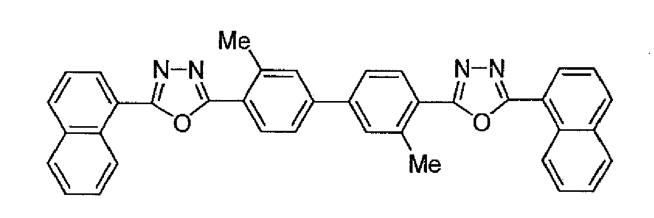


- Nitrogen-containing heterocyclic derivatives represented by the following formula:

R is an aryl group which has 6 to 60 carbon atoms and may have a substituent, a heteroaryl group which has 3 to 60 carbon atoms and may have a substituent, an alkyl group which has 1 to 20 carbon atoms, a haloalkyl group which has 1 to 20 carbon atoms, or an alkoxy group which has 1 to 20 carbon atoms; n is an integer of 0 to 5 and when n is an integer of 2 or more, Rs may be the same as or different from each other.
Adjacent Rs may be bonded to each other to form a substituted or unsubstituted carbocyclic aliphatic ring or a substituted or unsubstituted carbocyclic aromatic ring.
Ar14 is an aryl group which has 6 to 60 carbon atoms and may have a substituent, or a heteroaryl group which has 3 to 60 carbon atoms and may have a substituent.
Ar15 is a hydrogen atom, an alkyl group which has 1 to 20 carbon atoms, a haloalkyl group which has 1 to 20 carbon atoms, an alkoxy group which has 1 to 20 carbon atoms, an aryl group which has 6 to 60 carbon atoms and may have a substituent, or a heteroaryl group which has 3 to 60 carbon atoms and may have a substituent.
Provided that either one of Ar14 and Ar15 is a condensed cyclic group which has 10 to 60 carbon atoms and may have a substituent or a condensed heterocyclic group which has 3 to 60 carbon atoms and may have a substituent.
L1 and L2 are each a single bond, a condensed cyclic group which has 6 to 60 carbon atoms and may have a substituent, a condensed heterocyclic group which has 3 to 60 carbon atoms and may have a substituent, or a fluorenylene group which may have a substituent. - Nitrogen-containing heterocyclic derivatives represented by the following formula:
HAr-L3-Ar16-Ar17
wherein HAr is a nitrogen-containing heterocyclic ring with 3 to 40 carbon atoms which may have a substituent;
L3 is a single bond, an arylane group with 6 to 60 carbon atoms which may have a substituent, a heteroarylane group with 3 to 60 carbon atoms which may have a substituent or a fluorenylene group which may have a substituent;
Ar16 is a bivalent aromatic hydrocarbon group with 6 to 60 carbon atoms which may have a substituent; and
Ar17 is an aryl group with 6 to 60 carbon atoms which may have a substituent or a heteroaryl group with 3 to 60 carbon atoms which may have a substituent. - An electroluminescence device using a silacyclopentadiene derivative represented by the following formula, disclosed in
JP-A-09-087616 
- Silacyclopentadiene derivative represented by the following formula, disclosed in
JP-A-09-194487 
- Borane derivatives represented by the following formula, disclosed in
JP-A1-2000-040586 
- Compounds represented by the following formula, disclosed in
JP-A-10-088121 
-

- The metal complexes have the strong nature of an n-type semiconductor and great capability of injecting electrons. Further the energy generated at the time of forming a complex is small so that a metal is then strongly bonded to ligands in the complex formed and the fluorescent quantum efficiency becomes large as the emitting material.
- Specific examples of the rings A4 and A5 which form the ligands of the above formula include halogen atoms such as chlorine, bromine, iodine and fluorine; substituted or unsubstituted alkyl groups such as methyl, ethyl, propyl, butyl, sec-butyl, tert-butyl, pentyl, hexyl, heptyl, octyl, stearyl and trichloromethyl; substituted or unsubstituted aryl groups such as phenyl, naphthyl, 3-methylphenyl, 3-methoxyphenyl, 3-fluorophenyl, 3-trichloromethylphenyl, 3-trifluoromethylphenyl and 3-nitrophenyl; substituted or unsubstituted alkoxy groups such as methoxy, n-butoxy, tert-butoxy, trichloromethoxy, trifluoroethoxy, pentafluoropropoxy, 2,2,3,3-tetrafluoropropoxy, 1,1,1,3,3,3-hexafluoro-2-propoxy and 6-(perfluoroethyl)hexyloxy; substituted or unsubstituted aryloxy groups such as phenoxy, p-nitrophenoxy, p-tert-butylphenoxy, 3-fluorophenoxy, pentafluorophenyl and 3-trifluoromethylphenoxy; substituted or unsubstituted alkylthio groups such as methythio, ethylthio, tert-butylthio, hexylthio, octylthio and trifruoromethyltio; substituted or unsubstituted arylthio groups such as phenylthio, p-nitrophenylthio, p-tert-butylphenylthio, 3-fluorophenylthio, pentafluorophenylthio and 3-trifluoromethylphenylthio; a cyano group; a nitro group, an amino group; mono or di-substituted amino groups such as methylamino, dimethylamino, ethylamino, diethylamino, dipropylamino, dibutylamino and diphenylamino; acylamino groups such as bis(acetoxymethyl)amino, bis(acetoxyethyl)amino, bis(acetoxypropyl)amino and bis(acetoxybutyl)amino; a hydroxy group; a siloxy group; an acyl group; substituted or unsubstituted carbamoyl groups such as carbmoyl, methylcarbamoyl, dimethylcarbamoyl, ethylcarbamoyl, diethylcarbamoyl, propylcarbamoyl, butylcarbamoyl and phenylcarbamoyl; a carboxylic group; a sulfonic acid group; an imido group; cycloalkyl groups such as cyclopentyl and cyclohexyl; aryl groups such as phenyl, naphthyl, biphenyl, anthranyl, phenanthryl, fluorenyl and pyrenyl; and heterocyclic groups such as pyridinyl, pyrazinyl, pyrimidinyl, pryidazinyl, triazinyl, indolinyl, quinolinyl, acridinyl, pyrrolidinyl, dioxanyl, piperidinyl, morpholidinyl, piperazinyl, triathinyl, carbazolyl, furanyl, thiophenyl, oxazolyl, oxadiazolyl, benzooxazolyl, thiazolyl, thiadiazolyl, benzothiazolyl, triazolyl, imidazolyl, benzoimidazolyl and puranyl. Moreover the above-mentioned substituents may be bonded to each other to form a six-membered aryl or heterocyclic ring.
- As the hole transporting compound, known compounds may be used.
Specific examples thereof include triazole derivatives (seeUSP No. 3, 112, 197 and others), oxadiazole derivatives (seeUSP No. 3,189,447 and others), imidazole derivatives (seeJP-B-37-16096 USP No. 3,615,402 ,3,820,989 and3,542,544 ,JP-B-45-555 51-10983 JP-A-51-93224 55-17105 56-4148 55-108667 55-156953 56-36656 USP Nos. 3,180,729 and4,278,746 ,JP-A-55-88064 55-88065 49-105537 55-51086 56-80051 56-88141 57-45545 54-112637 55-74546 USP No. 3,615,404 ,JP-B-51-10105 46-3712 47-25336 JP-A-54-53435 54-110536 54-119925 USP Nos. 3,567,450 ,3,180,703 ,3,240,597 ,3,658,520 ,4,232,103 ,4,175,961 and4,012,376 ,JP-B-49-35702 39-27577 JP-A-55-144250 56-119132 56-22437 DE1,110,518 , and others), amino-substituted chalcone derivatives (seeUSP No. 3, 526, 501 , and others), oxazole derivatives (ones disclosed inUSP No. 3,257,203 , and others), styrylanthracene derivatives (seeJP-A-56-46234 JP-A-54-110837 USP No. 3,717,462 ,JP-A-54-59143 55-52063 55-52064 55-46760 55-85495 57-11350 57-148749 2-311591 JP-A-61-210363 61-228451 61-14642 61-72255 62-47646 62-36674 62-10652 62-30255 60-93455 60-94462 60-174749 60-175052 USP No. 4,950,950 ), polysilanes (JP-A-2-204996 JP-A-2-282263 JP-A-1-211399 - The formation of the N-doped layer makes it possible that the acceptor-containing layer withdraws a larger number of electrons to make the driving voltage of the organic EL device lower.
- The formation of the P-doped layer makes it possible that a larger number of holes are sent to the hole-transporting layer to make the driving voltage of the organic EL device lower.
- The formation of the stacked body composed of an N-doped layer and a P-doped layer makes it possible that the acceptor-containing layer withdraws a larger number of electrons and further a larger number of holes are sent to the hole-transporting layer to make the driving voltage of the organic EL device lower still.
- In the case that the buffer layer is a semiconductive inorganic compound layer, the semiconductive inorganic compound layer is preferably made of a transition metal oxide. Specific examples of the transition metal oxide include NbO, LaO, NdO, SmO, EuOx, MoO3, MoO2, ReO2, ReO3, OsO2, IrO2, and PtO2. Preferred are LiTi2O4, LiV2O4, ErxNbO3, LaTiO3, SrVO3, CaCrO3, SrxCrO3, AxMoO3, and AV2O5 wherein A = K, Cs, Rb, Sr, Na, Li or Ca.
The same advantageous effects as produced by the doped layer can also be expected by the formation of the semiconductive inorganic compound layer. - The following will describe the acceptor.
The acceptor is an easily-reducible organic compound.
The easiness of the reduction of a compound can be measured based on the reduction potential thereof. In the invention, the acceptor is preferably a compound having a reduction potential of -0.8 V or more, and is more preferably a compound having a higher reduction potential than that (approximately 0 V) of tetracyanoquinodimethane (TCNQ). The reduction potential is a reduction potential measured by use of a saturated calomel electrode (SCE) as a reference electrode. - The easily-reducible organic compound is preferably an organic compound having an electron-withdrawing substituent. Specific examples thereof include quinoide derivatives, pyrazine derivatives, arylborane derivatives, and imide derivatives. Examples of the quinoide derivatives include quinodimethane derivatives, thiopyrandioxide derivatives, thioxanthendioxide derivatives and quinone derivatives.
- Preferred quinoid derivatives include compounds of formulae (1a) to (1i). More preferred quinoid derivatives are compounds of formulae (1a) and (1b). These each are the hole-injecting material for an organic EL device of the invention.


- In formulae (1a) to (1i), R1 to R48 are each a hydrogen atom, halogen atom, fluoroalkyl group, cyano group, alkoxy group, alkyl group or aryl group, preferably a hydrogen atom or cyano group.
In formulae (1a) to (1i), X is an electron-withdrawing group of formulae (j) to (p), preferably (j), (k) or (l),
In formulae (1a) to (1i), Y is -N= or -CH=. - As the halogen of R1 to R48, fluorine and chlorine are preferred.
- As the fluoroalkyl group of R1 to R48, trifluoromethyl and pentafluoroethyl groups are preferred.
- As the alkoxy group of R1 to R48, methoxy, ethoxy, iso-propoxy and tert-butoxy groups are preferred.
As the alkyl group of R1 to R48, methyl, ethyl, propyl, iso-propyl, tert-butyl and cyclohexyl groups are preferred. - As the aryl group of R1 to R48, phenyl and naphthyl groups are preferred.
- The fluroalkyl, alkyl and aryl groups of R49 to R52 are the same as those of R1 to R48.
- As the heterocylce of R49 to R52, substituents shown by the following formulae are preferred.

- When R50 and R51 form a ring, X is preferably a substituent of the following formula,

- Specific examples of the quinoid derivatives include the following compounds.


- The arylborane derivatives include compounds of the following formula (2a) or (2b).

- In formulae (2a) and (2b), Ar1 to Ar8 are each an aryl group or heterocycle having an electron-withdrawing group.
As the aryl group having an electron-withdrawing group of Ar1 to Ar8, pentafluorophenyl, pentafluoronaphthyl and pentafluorophenyl groups are preferred.
As the heterocycle having an electron-withdrawing group of Ar1 to Ar8, quinoline, quinoxaline, pyridine and pyrazine rings are preferred. - Specific examples of the arylborane derivatives include the following compounds.

- Preferred examples of the arylborane derivatives include compounds having at least one fluorine as a substituent positioned on the aryl. Particularly preferred is tris β-(pentafluoronaphthyl)borane (PNB).
- The thiopyrane dioxide derivatives include compounds of the following formula (3a), and the thioxanthenedioxide derivatives include compounds of the following formula (3b).

- In formulae (3a) and (3b), R53 to R64 are each a hydrogen atom, halogen atom, fluoroalkyl group, cyano group, alkyl group or aryl group, preferably a hydrogen atom or cyano group.
In formulae (3a) and (3b), X shows an electron-withdrawing group, and is the same as X of formulae (1a) to (1i). X preferably has the structure of (i), (j) or (k). - The halogen, fluoroalkyl, alkyl and aryl groups of R53 to R64 are the same as those of R1 to R48.
- Specific examples of the thiopyranedioxide derivatives shown by formula (3a) and thioxanthenedioxide derivatives shown by formula (3b) are as follows.


- Furthermore, in formulae (1a) to (1i) and (3a) to (3b), the electron-withdrawing group X may be a substituent (x) or (y) represented by the following formulae:

- In the formula, Ar1 and Ar2 are a substituted or unsubstituted heterocycle, substituted or unsubstituted aryloxycarbonyl or aldehyde, and are preferably pyridine, pyrazine, or quinoxaline. Ar1 and Ar2 may be bonded to each other to form a 5-membered or 6-membered cyclic structure.
- Preferred examples of the imide derivatives include naphthalene tetracarboxylic acid diimide compounds and pyromellitic acid diimide compounds.
- In the invention, an acceptor is contained in the acceptor-containing layer so that the layer can transport electrons. The acceptor content is preferably more than 20% by weight of the total of the layer. In order to cause the electron mobility of the acceptor-containing layer to be more than 10-5, the acceptor content is more preferably 40% or more by weight, even more preferably 50% or more by weight.
- The acceptor-containing layer has electron-transportability, and this means that the layer is relatively electron-transportable rather than hole-transportable.
In order to confirm the electron-transportability of the acceptor-containing layer, various methods may be used. For example, the transportability can be confirmed by any one of the following methods (1) to (3): - (1) a method of sandwiching a thin film having a thickness of 2 to 10 µm and the same composition as the acceptor-containing layer between electrodes, then causing optical excitation therein by irradiating a laser ray from above the cathode, and then measuring the transient optical current (the time-of-flight or TOF method),
- (2) a method of sandwiching a thin film having the same composition as the acceptor-containing layer between electrodes, the cathode thereof being an electron-injecting electrode made of Mg:Ag, Al/LiF or the like, applying a step-form voltage thereto, and then measuring the electron mobility by determining the shape of the transient current, and
- (3) a method of sandwiching a thin film having the same composition as the acceptor-containing layer between electrodes wherein only electron injection is caused (for example, Al or Al/LiF), and then measuring the value of the current.
- The acceptor-containing layer exists as a continuous film formed by deposition. For example, the use of the above compounds enables formation of a continuous film by deposition. The "continuous film" is one in which its material continuously exists without gaps from the surface of the film to a substrate on which the film the formed.
The surface of the acceptor-containing layer preferably has a plane roughness (Ra) of 1.5 nm or less, more preferably 1.0 nm or less. The plane roughness can be determined under an atom force microscope (AFM).
Fig. 5 shows the states of a continuous film (a) and non-continuous film (b).
In a non-continuous film or a film having a large plane roughness (Fig. 5(b) ), when depositing an acceptor compound B' constituting an acceptor-containing layer 70', the grain size of the acceptor compound B' crystals becomes large. As a result, contact areas between the acceptor compound B' crystals and at the interfaces with upper and lower layers, e.g., hole-transportinglayer 30 andanode 10, may become smaller, whereby current is difficult to flow, leading to an increased driving voltage and decreased efficiency. - An electron-donating compound may be added to the acceptor-containing layer. The amount of the electron-donating compound added is preferably smaller than the concentration of the acceptor. For example, the amount thereof is from 1 to 20% by weight of the total of the layer.
The addition of the electron-donating compound makes it possible to improve the electron-conductivity of the acceptor-containing layer to make the driving voltage of the organic EL device lower and prevent the hole-transporting layer from being deteriorated.
Examples of the electron-donating compound include inorganic materials such as alkali metals, alkaline earth metals, rare earth elements, Al, Ag, Cu and In; and organic materials such as anilines, phenylenediamines, benzidines (such as N,N,N',N'-tetraphenylbenzidine, N,N'-bis-(3-methylphenyl)-N,N'-bis-(phenyl)-benzidine, and N,N'-di(naphthalene-1-yl)-N,N'-diphenyl-benzidine), compounds having as their skeleton an aromatic tertiary amine such as triphenylamines (such as triphenylamine, 4,4',4"-tris(N,N-diphenyl-amino)-triphenylamine, 4,4',4"-tris(N-3-methylphenyl-N-phenyl-amino)-triphenylamine, and 4,4',4"-tris(N-(1-naphthyl)-N-phenyl-amino)-triphenylamine), and triphenyldiamines (such as N,N'-di-(4-methyl-phenyl)-N,N'-diphenyl-1,4-phenylenediamine), condensed polycyclic compounds (these condensed polycyclic compounds may have a substituent) such as pyrene, perylene, anthracene, tetracene and pentacene, and TTF (tetrathiafluvalene). - Preferred electron-donating compounds include compounds of the following formula (4).

- In formula (4), R65 to R68 are each a hydrogen atom, halogen atom, alkyl group, aryl group, heterocycle or diarylamino group and may be joined together to form a phenyl or naphthyl group.
In formula (4), R69 to R70 are each a hydrogen atom, halogen atom or alkyl group. - As the halogen atom of R65 to R68, fluorine and chlorine are preferred.
- As the alkyl group of R65 to R68, methyl, ethyl, i-propyl, tert-butyl and cyclohexyl groups are preferred.
- As the aryl group of R65 to R68, phenyl, naphthyl, fluorenyl, biphenyl and terphenyl groups are preferred.
- As the heterocycle of R65 to R68, a carbazolyl group is preferred.
- As the diarylamino group of R65 to R68, diphenylamino, phenyl-biphenylamino and biphenylamino groups are preferred.
- The halogen atom and alkyl group of R69 to R70 are the same as those of R65 to R68.
- The organic EL device of the invention preferably contains the compound of formula (4) in a hole-transporting layer. If the hole-transporting layer contains the compound, the organic EL device can emit light with a high efficiency at a low voltage.
- A compound A shown below was selected as a material for forming an acceptor-containing layer. In a cyclic voltammetric measurement thereof wherein a saturated calomel electrode (SCE) was used as a reference electrode, the reduction potential thereof was 0.71 V.

- Al as an electrode material and the compound A as a material for forming an acceptor-containing layer were each mounted on a tungstent filament and a molybdenum heating boat of a vacuum deposition device, respectively. A 150 nm thick Al layer, a 200 nm thick layer made of the compound A, and a 150 nm thick Al layer were formed on a 0.7 mm thick glass substrate in this order. A voltage of 1 V was applied across the two Al electrodes, and the value of the current flowing therein was measured. The value was 251 mA/cm2. Further, 250 nm thick Au layers, which Au was an electrode material, and a 100 nm thick layer made of the compound A were formed on the 0.7 mm thick glass substrate. The Au layers spaced 1 mm apart. A voltage of 10 V was applied across the two Au electrodes, and the value of the current flowing therein was measured. The value was 4 A/cm2. For F4-TCNQ, similar measurement was conducted. The resultant current value was 15.7 mA/cm2.
- An ITO film was formed on a 0.7 mm thick glass substrate by sputtering to a thickness of 130 nm. The substrate was subjected to ultrasonic cleaning in isopropyl alcohol for 5 minutes, and cleaned with ultraviolet ozone for 30 minutes. Then the substrate with the ITO electrode was mounted on a substrate holder in a vacuum vapor deposition apparatus.
The compound A as a material for an acceptor-containing layer, HT1 as a hole-transporting material, Alq3 as a material for an emitting layer and an electron-transporting material, LiF as an electron-injecting material and Al as a cathode material were mounted on respective molybdenum heating boats in advance.
- First, a compound A film which functioned as the acceptor-containing layer was formed in a thickness of 36 nm. After forming the acceptor-containing layer, a HT film which functioned as the hole-transporting layer was formed in a thickness of 40 nm. After forming the HT film, an Alq3 film was formed in a thickness of 50 nm as the emitting layer and electron-transporting layer. Then an LiF film was deposited to a thickness of 1.2 nm as the electron-injecting layer, and an Al film which functioned as the cathode was formed thereon in a thickness of 250 nm to obtain an organic EL device. In the above fabrication, when the compound A film was formed to 36 nm on the ITO film, the compound A film was observed under a transmission electron microscope (TEM) (HF-2200, manufactures by Hitachi, Ltd.). The film was confirmed to be a continuous film (
Fig. 6 ). Note that a carbon layer for deposition was formed to reduce damage due to thin film processing and to impart electrical conductivity. The compound A film was measured for plane roughness (Ra) under an atom force microscope (AFM) (AutoProbe M5, manufactured by TM Microscopes). The Ra was 0.7 nm. - An organic EL device was fabricated in the same manner as in Example 1 except that a 5 nm thick Al film was formed as an anode on the ITO film and the thickness of the HT1 film was 15 nm.
- An organic EL device was fabricated in the same manner as in Example 1 except that no acceptor-containing layer film was formed, and the thickness of the HT1 film as the transporting layer was 106 nm.
- An organic EL device was fabricated in the same manner as in Comparative Example 1 except that F4-TCNQ was used in the acceptor-containing layer. When the 36 nm thick F4-TCNQ film, which thickness was determined with a film thickness meter, was formed on the ITO film, the F4-TCNQ film was observed under a TEM. The film was confirmed to have continuous gaps which reached the substrate (
Fig. 7 ). The F4-TCNQ film was measured for plane roughness of the surface under an AFM to be 12.9 nm. - The following evaluations were conducted for the organic EL devices obtained in Examples 1 to 4, and Comparative Examples 1 and 2. The results are shown in Table 1.
- (1) Voltage (unit:V) at the time of applying a current between ITO and Al such that a current density was 10 mA/cm2 was measured.
- (2) Luminous efficiency (unit:cd/A) was calculated from EL spectrum at the time of applying voltage at a current density of 10 mA/cm2.
- Table 1 confirmed that the voltages were lowered, and equal or more luminous efficiencies were shown in Examples 1 and 2 compared with Comparative Examples 1 and 2. This was probably caused by the difference in the film state between the acceptor-containing layers as observed by a TEM and AFM. This shows that the continuity of a film or smoothness of a surface influenced voltage or efficiency.
- Moreover, as shown in Example 2, even an electrode having a work function smaller than 4.8 eV such as Al electrode (work function of 4.1 eV) can emit light with a similar luminance at a lower voltage compared to heretofore. Considering that conventionally emissions could be observed only at a voltage exceeding 10 V, this shows that the invention has a great advantage.
- The above Examples describe the bottom emission structure, but it is apparent that the invention can also be applied to the top emission structure. The invention can especially have a structure of reflective metal layer/acceptor-containing layer/organic medium including an emitting layer/light transparent cathode. For the reflective metal, Al, Ag, Ni, Mo, W, Ta, Ti, Cr and alloys thereof are often used. However, even when using metal or alloy layers having a work function smaller than 4.8 eV, light can be emitted at a low voltage. Conventionally where a reflective metal directly contacts a hole-transporting layer or hole-injecting layer, the voltage substantially increases.
- An organic EL device was fabricated in the same manner as in Example 1 except that the compound (B) of the following formula was used as the acceptor-containing layer.
- An organic EL device was fabricated in the same manner as in Example 1 except that the compound (C) of the following formula was used as the acceptor-containing layer.
- An organic EL device was fabricated in the same manner as in Example 1 except that the compound (D) of the following formula was used as the acceptor-containing layer.
-

- The organic EL devices fabricated in Examples 3 to 5 were evaluated in the same manner as in Example 1. Table 1 shows the results.
-
Table 1 Anode Acceptor-containing layer Hole-transporting layer Setting layer (Electron-transporting layer) Electron-injecting layer Cathode Voltage (V) Luminous efficiency (cd/A) Example 1 ITO Compound A HT1 Alq3 LiF A1 6.2 1.11 Example 2 ITO/A1 Compound A HT1 Alq3 LiF A1 5.9 1.87 Example 3 ITO Compound B HT1 Alq3 LiF A1 6.6 1.14 Example 4 ITO Compound C HT1 Alq3 LiF A1 7.1 1.17 Example 5 ITO Compound D HT1 Alq3 LiF A1 6.4 1.12 Comparative Example 1 ITO - HT1 Alq3 LiF A1 8.6 1.08 Comparative Example 2 ITO F4-TCNQ HT1 Alq3 LiF A1 2.4 0.0003 - An ITO film was formed on a 0.7 mm thick glass substrate by using sputtering to a thickness of 130 nm. The substrate was subjected to ultrasonic cleaning in isopropyl alcohol for 5 minutes, and cleaned with ultraviolet ozone for 30 minutes. Then the substrate with the ITO electrode was mounted on a substrate holder in a vacuum vapor deposition apparatus.
The compound A as a material for an acceptor-containing layer, HT1 as a first hole-transporting material, HT2 as a second hole-transporting material, BH as a host material for an emitting layer, BD as a blue emitting material, Alq3 as an electron-transporting material, LiF as an electron-injecting material and Al as a cathode material were mounted on respective molybdenum heating boats in advance. Moreover, MoO3 was mounted as a semiconductive oxide material.


- First, a compound A film which functioned as the acceptor-containing layer was formed in a thickness of 10 nm. After forming the acceptor-containing layer, a HT2 film which functioned as the second hole-transporting layer was formed in a thickness of 50 nm. Subsequently, a HT1 film which functioned as the first hole-transporting layer was formed in a thickness of 20 nm. After forming the HT1 film, a compound BH and compound BD were co-deposited in a thickness of 40 nm at a ratio of 40:2 as the emitting layer. An Alq3 film was formed thereon in a thickness of 20 nm as the electron-transporting layer. Then an LiF film was deposited to a thickness of 1 nm as the electron-injecting layer, and an Al film which functioned as the cathode was formed thereon in a thickness of 150 nm to obtain an organic EL device.
- An organic EL device was fabricated in the same manner as in Example 6 except that no acceptor-containing layer film was formed, and the thickness of the HT2 film as the second hole-transporting layer was 60 nm.
- An organic EL device was fabricated in the same manner as in Example 6 except that after forming the acceptor-containing layer, a P-doped layer was formed in a thickness of 50 nm at a ratio of the second hole-transporting material HT2 to compound A of 100:5, and the HT1 film as the first hole-transporting layer was then formed in a thickness of 20 nm.
- An organic EL device was fabricated in the same manner as in Example 6 except that after forming the acceptor-containing layer, a molybdenum oxide MoO3 film was formed in a thickness of 5 nm.
- An organic EL device was fabricated in the same manner as in Example 6 except that an Al film was formed on the ITO film in a thickness of 5 nm as an anode, and the thickness of the HT2 film was 15 nm.
- Table 2 shows the structures of the organic EL devices fabricated in Examples 6 to 9 and comparative example 3. These organic EL devices were evaluated in the same manner as in Example 1. Table 3 shows the results.
-
Table 2 Anode Acceptor-containing layer Semi-conductive oxide layer P-doped layer Second hole-transporting layer First hole-transporting layer Emitting layer Electron-transporting layer Electron-injecting layer Cathode Example 6 ITO Compound A - - HT2 HT1 BH/BD Alq3 LiF Al Comparative Example 3 ITO - - - HT2 HT1 BH/BD Alq3 LiF Al Example 7 ITO Compound A - HT2/ Compound A - HT1 BH/BD Alq3 LiF Al Example 8 ITO Compound A MoO3 - HT2 HT1 BH/BD Alq3 LiF Al Example 9 ITO/Al Compound A - - HT2 HT1 BH/BD Alq3 LiF Al -
Table 3 Voltage (v) CIE x CIE y Luminous efficiency (cd/A) Example 6 6.3 0.15 0.17 6.1 Comparative Example 3 6.9 0.15 0.17 6.3 Example 7 5.8 0.15 0.18 6.6 Example 8 6.2 0.15 0.17 6.0 Example 9 6.0 0.12 0.18 7.9 - The organic EL device of the invention can be used as organic EL materials for various colors including blue. The device can be used in fields such as various display devices, displays, back light, light sources, signs, signboards and interior; and especially suitable as a display device for color display.
Claims (15)
- An organic electroluminescence device comprising:an emitting layer between an anode and a cathode,an acceptor-containing layer, anda hole-transporting layer,the acceptor-containing layer and the hole-transporting layer being disposed between the anode and the emitting layer in this order from the anode,the acceptor-containing layer being a continuous film formed by deposition.
- The organic electroluminescence device according to claim 1, wherein the acceptor-containing layer has a surface with a surface roughness (Ra) of 1.5 nm or less.
- The organic electroluminescence device according to claim 1 or 2, wherein the reduction potential of the acceptor-containing layer is larger than the reduction potential of tetracyanoquinodimethane.
- The organic electroluminescence device according to any one of claims 1 to 3, wherein the acceptor of the acceptor-containing layer is a quinoid derivative of formulae (1a) to (li),


X is an electron-withdrawing group of formulae (j) to (p),
Y is -N= or -CH=.
- The organic electroluminescence device according to any one of claims 1 to 3, wherein the acceptor of the acceptor-containing layer is an arylborane derivative of formula (2a) or (2b),

- The organic electroluminescence device according to any one of claims 1 to 3, wherein the acceptor of the acceptor-containing layer is a thiopyranedioxide derivative of formula (3a) or a thioxanthenedioxide derivative of formula (3b),

X is an electron-withdrawing group of formulae (j) to (p),
- The organic electroluminescence device according to any one of claims 1 to 6, wherein an electron-donating compound is added to the acceptor-containing layer in a concentration lower than the concentration of the acceptor.
- The organic electroluminescence device according to claim 7, wherein the electron-donating compound is a phenylenediamine compound of formula (4),

R69 to R70 are each a hydrogen atom, halogen atom or alkyl group. - The organic electroluminescence device according to any one of claims 1 to 8, wherein the hole-transporting layer is a phenylenediamine compound of formula (4),

R69 to R70 are each a hydrogen atom, halogen atom or alkyl group. - The organic electroluminescence device according to any one of claims 1 to 9, wherein a buffer layer is interposed between the acceptor-containing layer and the hole-transporting layer.
- The organic electroluminescence device according to claim 10, wherein the buffer layer is a doped layer.
- The organic electroluminescence device according to claim 11, wherein the doped layer is an N-doped layer and/or a P-doped layer.
- The organic electroluminescence device according to claim 10, wherein the buffer layer is a semiconductive oxide layer.
- The organic electroluminescence device according to any one of claims 1 to 13, wherein electrons are transported from the buffer layer or a contacting surface between the acceptor-containing layer and the hole-transporting layer into the acceptor-containing layer toward the anode, and
holes are transported from the buffer layer or the contacting surface between the acceptor-containing layer and the hole-transporting layer into the hole-transporting layer toward the emitting layer. - A hole-injecting material for an organic electroluminescence device comprising a quinoid derivative of formulae (1a) to (li) recited in claim 4.
Applications Claiming Priority (3)
| Application Number | Priority Date | Filing Date | Title |
|---|---|---|---|
| JP2005332652 | 2005-11-17 | ||
| JP2006104255 | 2006-04-05 | ||
| PCT/JP2006/322660 WO2007058172A1 (en) | 2005-11-17 | 2006-11-14 | Organic electroluminescent device |
Publications (1)
| Publication Number | Publication Date |
|---|---|
| EP1950817A1 true EP1950817A1 (en) | 2008-07-30 |
Family
ID=38048558
Family Applications (1)
| Application Number | Title | Priority Date | Filing Date |
|---|---|---|---|
| EP06842815A Withdrawn EP1950817A1 (en) | 2005-11-17 | 2006-11-14 | Organic electroluminescent device |
Country Status (5)
| Country | Link |
|---|---|
| EP (1) | EP1950817A1 (en) |
| JP (1) | JPWO2007058172A1 (en) |
| KR (1) | KR20080069190A (en) |
| TW (1) | TW200739987A (en) |
| WO (1) | WO2007058172A1 (en) |
Cited By (5)
| Publication number | Priority date | Publication date | Assignee | Title |
|---|---|---|---|---|
| US20100133996A1 (en) * | 2007-05-09 | 2010-06-03 | Dongjin Semichem Co., Ltd | Novel anthracene typed compound and the organic electroluminescence display device using the same |
| WO2013153025A1 (en) | 2012-04-12 | 2013-10-17 | Siemens Aktiengesellschaft | Organic electronic components having organic superdonors having at least two coupled carbene groups and use thereof as an n-type dopants |
| US8963132B2 (en) | 2010-03-25 | 2015-02-24 | Universal Display Corporation | Solution processable doped triarylamine hole injection materials |
| US11495745B2 (en) | 2017-10-20 | 2022-11-08 | Lg Chem, Ltd. | Compound and organic light emitting device comprising same |
| US11767299B2 (en) | 2017-06-23 | 2023-09-26 | Merck Patent Gmbh | Materials for organic electroluminescent devices |
Families Citing this family (9)
| Publication number | Priority date | Publication date | Assignee | Title |
|---|---|---|---|---|
| WO2009020095A1 (en) * | 2007-08-06 | 2009-02-12 | Idemitsu Kosan Co., Ltd. | Aromatic amine derivative and organic electroluminescent device using the same |
| JP5515234B2 (en) * | 2008-03-31 | 2014-06-11 | 住友化学株式会社 | Intermediate layer forming coating liquid, method for producing organic electroluminescent element, and organic electroluminescent element |
| KR101097316B1 (en) * | 2009-10-12 | 2011-12-23 | 삼성모바일디스플레이주식회사 | organic light emitting device |
| JP2014049696A (en) * | 2012-09-03 | 2014-03-17 | Nippon Hoso Kyokai <Nhk> | Organic electroluminescent element |
| KR102195601B1 (en) * | 2013-09-09 | 2020-12-30 | 엘지디스플레이 주식회사 | Organic Compound having hole injecting characteristic and Organic Light Emitting Device and Display Device using the same |
| KR102181311B1 (en) * | 2013-12-03 | 2020-11-23 | 엘지디스플레이 주식회사 | Organic compounds and organic light emitting diode device comprising the same |
| KR102311498B1 (en) * | 2014-12-30 | 2021-10-12 | 엘지디스플레이 주식회사 | Organic Compound having hole injecting characteristic and Organic Light Emitting Device and Display Device using the same |
| WO2019078620A1 (en) * | 2017-10-20 | 2019-04-25 | 주식회사 엘지화학 | Novel compound and organic light-emitting device using same |
| KR102192368B1 (en) * | 2018-02-28 | 2020-12-17 | 주식회사 엘지화학 | Organic light emitting device |
Family Cites Families (87)
| Publication number | Priority date | Publication date | Assignee | Title |
|---|---|---|---|---|
| NL99369C (en) | 1956-06-04 | |||
| LU35237A1 (en) | 1956-06-27 | |||
| US3180729A (en) | 1956-12-22 | 1965-04-27 | Azoplate Corp | Material for electrophotographic reproduction |
| BE581861A (en) | 1958-08-20 | |||
| NL250330A (en) | 1959-04-09 | |||
| US3240597A (en) | 1961-08-21 | 1966-03-15 | Eastman Kodak Co | Photoconducting polymers for preparing electrophotographic materials |
| US3180703A (en) | 1963-01-15 | 1965-04-27 | Kerr Mc Gee Oil Ind Inc | Recovery process |
| JPS45555B1 (en) | 1966-03-24 | 1970-01-09 | ||
| JPS463712B1 (en) | 1966-04-14 | 1971-01-29 | ||
| US3526501A (en) | 1967-02-03 | 1970-09-01 | Eastman Kodak Co | 4-diarylamino-substituted chalcone containing photoconductive compositions for use in electrophotography |
| US3542544A (en) | 1967-04-03 | 1970-11-24 | Eastman Kodak Co | Photoconductive elements containing organic photoconductors of the triarylalkane and tetraarylmethane types |
| US3567450A (en) | 1968-02-20 | 1971-03-02 | Eastman Kodak Co | Photoconductive elements containing substituted triarylamine photoconductors |
| US3658520A (en) | 1968-02-20 | 1972-04-25 | Eastman Kodak Co | Photoconductive elements containing as photoconductors triarylamines substituted by active hydrogen-containing groups |
| US3615404A (en) | 1968-04-25 | 1971-10-26 | Scott Paper Co | 1 3-phenylenediamine containing photoconductive materials |
| CA917980A (en) | 1969-06-20 | 1973-01-02 | J. Fox Charles | Alkylaminoaromatic organic photoconductors |
| US3717462A (en) | 1969-07-28 | 1973-02-20 | Canon Kk | Heat treatment of an electrophotographic photosensitive member |
| BE756375A (en) | 1969-09-30 | 1971-03-01 | Eastman Kodak Co | NEW PHOTOCONDUCTIVE COMPOSITION AND PRODUCT CONTAINING IT FOR USE IN ELECTROPHOTOGRAPHY |
| BE756943A (en) | 1969-10-01 | 1971-03-16 | Eastman Kodak Co | NEW PHOTOCONDUCTIVE COMPOSITIONS AND PRODUCTS CONTAINING THEM, USED IN PARTICULAR IN ELECTROPHOTOGRAPHY |
| JPS4725336B1 (en) | 1969-11-26 | 1972-07-11 | ||
| JPS5110983B2 (en) | 1971-09-10 | 1976-04-08 | ||
| GB1413352A (en) | 1972-02-09 | 1975-11-12 | Scott Paper Co | Electrophotographic material |
| US3837851A (en) | 1973-01-15 | 1974-09-24 | Ibm | Photoconductor overcoated with triarylpyrazoline charge transport layer |
| GB1505409A (en) | 1974-12-20 | 1978-03-30 | Eastman Kodak Co | Photoconductive compositions |
| US4012376A (en) | 1975-12-29 | 1977-03-15 | Eastman Kodak Company | Photosensitive colorant materials |
| US4175961A (en) | 1976-12-22 | 1979-11-27 | Eastman Kodak Company | Multi-active photoconductive elements |
| JPS5453435A (en) | 1977-10-01 | 1979-04-26 | Yoshikatsu Kume | Portable bicycle equipped with foldable type triangle frame |
| US4150987A (en) | 1977-10-17 | 1979-04-24 | International Business Machines Corporation | Hydrazone containing charge transport element and photoconductive process of using same |
| JPS54112637A (en) | 1978-02-06 | 1979-09-03 | Ricoh Co Ltd | Electrophotographic photoreceptor |
| JPS54110837A (en) | 1978-02-17 | 1979-08-30 | Ricoh Co Ltd | Electrophotographic photoreceptor |
| JPS54110536A (en) | 1978-02-20 | 1979-08-30 | Ichikoh Ind Ltd | Device for time-lag putting out room lamp for motorcar |
| JPS54119925A (en) | 1978-03-10 | 1979-09-18 | Ricoh Co Ltd | Photosensitive material for electrophotography |
| JPS6028342B2 (en) | 1978-06-21 | 1985-07-04 | コニカ株式会社 | electrophotographic photoreceptor |
| JPS6060052B2 (en) | 1978-07-21 | 1985-12-27 | コニカ株式会社 | electrophotographic photoreceptor |
| JPS5551086A (en) | 1978-09-04 | 1980-04-14 | Copyer Co Ltd | Novel pyrazoline compound, its preparation, and electrophotographic photosensitive substance comprising it |
| JPS5546760A (en) | 1978-09-29 | 1980-04-02 | Ricoh Co Ltd | Electrophotographic photoreceptor |
| JPS5552064A (en) | 1978-10-13 | 1980-04-16 | Ricoh Co Ltd | Electrophotographic receptor |
| JPS5552063A (en) | 1978-10-13 | 1980-04-16 | Ricoh Co Ltd | Electrophotographic receptor |
| JPS5574546A (en) | 1978-11-30 | 1980-06-05 | Ricoh Co Ltd | Electrophotographic photoreceptor |
| JPS5588064A (en) | 1978-12-05 | 1980-07-03 | Konishiroku Photo Ind Co Ltd | Electrophotographic receptor |
| JPS5588065A (en) | 1978-12-12 | 1980-07-03 | Konishiroku Photo Ind Co Ltd | Electrophotographic receptor |
| JPS5585495A (en) | 1978-12-18 | 1980-06-27 | Pacific Metals Co Ltd | Method of composting organic waste |
| JPS55108667A (en) | 1979-02-13 | 1980-08-21 | Ricoh Co Ltd | Electrophotographic receptor |
| US4233384A (en) | 1979-04-30 | 1980-11-11 | Xerox Corporation | Imaging system using novel charge transport layer |
| JPS6035058B2 (en) | 1979-05-17 | 1985-08-12 | 三菱製紙株式会社 | Organic photo-semiconductor electrophotographic materials |
| JPS564148A (en) | 1979-06-21 | 1981-01-17 | Konishiroku Photo Ind Co Ltd | Electrophotographic receptor |
| JPS5622437A (en) | 1979-08-01 | 1981-03-03 | Ricoh Co Ltd | Electrophotographic receptor |
| US4232103A (en) | 1979-08-27 | 1980-11-04 | Xerox Corporation | Phenyl benzotriazole stabilized photosensitive device |
| JPS5636656A (en) | 1979-09-03 | 1981-04-09 | Mitsubishi Paper Mills Ltd | Electrophotographic material |
| JPS5646234A (en) | 1979-09-21 | 1981-04-27 | Ricoh Co Ltd | Electrophotographic receptor |
| US4273846A (en) | 1979-11-23 | 1981-06-16 | Xerox Corporation | Imaging member having a charge transport layer of a terphenyl diamine and a polycarbonate resin |
| JPS5680051A (en) | 1979-12-04 | 1981-07-01 | Ricoh Co Ltd | Electrophotographic receptor |
| JPS5688141A (en) | 1979-12-20 | 1981-07-17 | Konishiroku Photo Ind Co Ltd | Electrophotographic receptor |
| JPS6034099B2 (en) | 1980-06-24 | 1985-08-07 | 富士写真フイルム株式会社 | electrophotographic photoreceptor |
| JPS6059590B2 (en) | 1980-09-03 | 1985-12-25 | 三菱製紙株式会社 | electrophotographic photoreceptor |
| JPS57148749A (en) | 1981-03-11 | 1982-09-14 | Fuji Photo Film Co Ltd | Electrophotographic receptor |
| JPS6093455A (en) | 1983-10-28 | 1985-05-25 | Fuji Xerox Co Ltd | Developer for electrophotography |
| JPS6094462A (en) | 1983-10-28 | 1985-05-27 | Ricoh Co Ltd | Stilbene derivative and production thereof |
| JPS60174749A (en) | 1984-02-21 | 1985-09-09 | Ricoh Co Ltd | Styryl compound and preparation thereof |
| JPS60175052A (en) | 1984-02-21 | 1985-09-09 | Ricoh Co Ltd | Electrophotographic sensitive body |
| JPS6114642A (en) | 1984-06-29 | 1986-01-22 | Konishiroku Photo Ind Co Ltd | Electrophotographic sensitive body |
| JPS6172255A (en) | 1984-09-14 | 1986-04-14 | Konishiroku Photo Ind Co Ltd | Electrophotographic sensitive body |
| JPS61210363A (en) | 1985-03-15 | 1986-09-18 | Canon Inc | Electrophotographic sensitive body |
| JPS61228451A (en) | 1985-04-03 | 1986-10-11 | Canon Inc | Electrophotographic sensitive body |
| JPS6210652A (en) | 1985-07-08 | 1987-01-19 | Minolta Camera Co Ltd | Photosensitive body |
| JPS6230255A (en) | 1985-07-31 | 1987-02-09 | Minolta Camera Co Ltd | Electrophotographic sensitive body |
| JPS6236674A (en) | 1985-08-05 | 1987-02-17 | Fuji Photo Film Co Ltd | Electrophotographic sensitive body |
| JPS6247646A (en) | 1985-08-27 | 1987-03-02 | Konishiroku Photo Ind Co Ltd | Photosensitive body |
| JPH01211399A (en) | 1988-02-19 | 1989-08-24 | Toshiba Corp | Dynamic shift register with scanning function |
| JPH02282263A (en) | 1988-12-09 | 1990-11-19 | Nippon Oil Co Ltd | Hole transferring material |
| JP2727620B2 (en) | 1989-02-01 | 1998-03-11 | 日本電気株式会社 | Organic thin film EL device |
| US5653713A (en) | 1989-04-24 | 1997-08-05 | Michelson; Gary Karlin | Surgical rongeur |
| US4950950A (en) | 1989-05-18 | 1990-08-21 | Eastman Kodak Company | Electroluminescent device with silazane-containing luminescent zone |
| JPH02311591A (en) | 1989-05-25 | 1990-12-27 | Mitsubishi Kasei Corp | Organic electroluminescent element |
| JP2846503B2 (en) * | 1990-06-14 | 1999-01-13 | 出光興産株式会社 | Device thin film electrode, electroluminescent device having the same, and methods of manufacturing the same |
| JP2921382B2 (en) * | 1994-02-21 | 1999-07-19 | 住友電気工業株式会社 | Organic hole transport membrane |
| JP2918150B2 (en) | 1995-07-17 | 1999-07-12 | チッソ株式会社 | Organic electroluminescent device using silacyclopentadiene derivative |
| JP3677850B2 (en) | 1996-01-12 | 2005-08-03 | チッソ株式会社 | Silacyclopentadiene derivative |
| JP2982699B2 (en) | 1995-08-04 | 1999-11-29 | 東洋インキ製造株式会社 | Material for forming electron injection layer of multilayer organic electroluminescence device |
| JPH10255980A (en) * | 1997-03-10 | 1998-09-25 | Fuji Electric Co Ltd | Organic thin-film light emitting device |
| JPH11251067A (en) | 1998-03-02 | 1999-09-17 | Junji Kido | Organic electroluminescence element |
| JP3716096B2 (en) | 1998-04-02 | 2005-11-16 | 三菱重工業株式会社 | Pulverized coal separator |
| JP4824848B2 (en) * | 2000-02-29 | 2011-11-30 | 淳二 城戸 | Organic electroluminescent device, organic electroluminescent device group, and method for identifying emission spectrum thereof |
| JP3664069B2 (en) * | 1999-12-24 | 2005-06-22 | 松下電器産業株式会社 | Organic electroluminescence device |
| JP4396115B2 (en) * | 2002-03-22 | 2010-01-13 | 三菱化学株式会社 | Polymer compound, 1,4-phenylenediamine derivative, charge transport material, organic electroluminescent element material, and organic electroluminescent element |
| JP5024498B2 (en) | 2003-09-11 | 2012-09-12 | 日産化学工業株式会社 | Charge transporting varnish, charge transporting thin film, and organic electroluminescence device |
| JP4300176B2 (en) * | 2003-11-13 | 2009-07-22 | ローム株式会社 | Organic electroluminescent device |
| JP2005294188A (en) * | 2004-04-05 | 2005-10-20 | Sony Corp | Display element |
-
2006
- 2006-11-14 KR KR1020087011705A patent/KR20080069190A/en not_active Application Discontinuation
- 2006-11-14 WO PCT/JP2006/322660 patent/WO2007058172A1/en active Application Filing
- 2006-11-14 JP JP2007545242A patent/JPWO2007058172A1/en active Pending
- 2006-11-14 EP EP06842815A patent/EP1950817A1/en not_active Withdrawn
- 2006-11-17 TW TW095142633A patent/TW200739987A/en unknown
Non-Patent Citations (1)
| Title |
|---|
| See references of WO2007058172A1 * |
Cited By (6)
| Publication number | Priority date | Publication date | Assignee | Title |
|---|---|---|---|---|
| US20100133996A1 (en) * | 2007-05-09 | 2010-06-03 | Dongjin Semichem Co., Ltd | Novel anthracene typed compound and the organic electroluminescence display device using the same |
| US8963132B2 (en) | 2010-03-25 | 2015-02-24 | Universal Display Corporation | Solution processable doped triarylamine hole injection materials |
| WO2013153025A1 (en) | 2012-04-12 | 2013-10-17 | Siemens Aktiengesellschaft | Organic electronic components having organic superdonors having at least two coupled carbene groups and use thereof as an n-type dopants |
| DE102012205945A1 (en) | 2012-04-12 | 2013-10-17 | Siemens Aktiengesellschaft | Organic super donors with at least two coupled carbene groups and their use as n-dopants |
| US11767299B2 (en) | 2017-06-23 | 2023-09-26 | Merck Patent Gmbh | Materials for organic electroluminescent devices |
| US11495745B2 (en) | 2017-10-20 | 2022-11-08 | Lg Chem, Ltd. | Compound and organic light emitting device comprising same |
Also Published As
| Publication number | Publication date |
|---|---|
| KR20080069190A (en) | 2008-07-25 |
| TW200739987A (en) | 2007-10-16 |
| WO2007058172A1 (en) | 2007-05-24 |
| JPWO2007058172A1 (en) | 2009-04-30 |
Similar Documents
| Publication | Publication Date | Title |
|---|---|---|
| JP4970934B2 (en) | Organic electroluminescence device | |
| US7737625B2 (en) | Organic electroluminescent device with carrier blocking layer interposed between two emitting layers | |
| JP4509211B2 (en) | ORGANIC ELECTROLUMINESCENT DEVICE HAVING TWO LIGHT EMITTING LAYERS THROUGH ELECTRON BARRIER | |
| EP1950817A1 (en) | Organic electroluminescent device | |
| US8076839B2 (en) | Organic electroluminescence device | |
| EP2045848B1 (en) | Organic electroluminescent device material and organic electroluminescent device | |
| US8119828B2 (en) | Material for an organic electroluminescence device and an organic electroluminescence device | |
| EP2053672A1 (en) | Organic electroluminescence device | |
| EP1578175B1 (en) | Organic electroluminescence element | |
| EP1947708A1 (en) | Organic electroluminescent element | |
| EP2213662A1 (en) | Azaindenofluorenedione derivative, organic electroluminescent device material, and organic electroluminescent device | |
| US7888865B2 (en) | Organic electroluminescent device and display having multiple emitting layers | |
| EP2000456A9 (en) | Material for organic electroluminescent device and organic electroluminescent device using the same | |
| US20070134511A1 (en) | Organic electroluminescence device | |
| EP2034803A1 (en) | Organic electroluminescence element | |
| US20070108894A1 (en) | Organic electroluminescent device | |
| JP2008085363A (en) | White organic electroluminescence device | |
| EP1653783A1 (en) | White organic electroluminescence element |
Legal Events
| Date | Code | Title | Description |
|---|---|---|---|
| PUAI | Public reference made under article 153(3) epc to a published international application that has entered the european phase |
Free format text: ORIGINAL CODE: 0009012 |
|
| 17P | Request for examination filed |
Effective date: 20080514 |
|
| AK | Designated contracting states |
Kind code of ref document: A1 Designated state(s): AT BE BG CH CY CZ DE DK EE ES FI FR GB GR HU IE IS IT LI LT LU LV MC NL PL PT RO SE SI SK TR |
|
| STAA | Information on the status of an ep patent application or granted ep patent |
Free format text: STATUS: THE APPLICATION HAS BEEN WITHDRAWN |
|
| 18W | Application withdrawn |
Effective date: 20090226 |