EP1886969A2 - Methods of fabrication of wafer-level vacuum packaged devices - Google Patents
Methods of fabrication of wafer-level vacuum packaged devices Download PDFInfo
- Publication number
- EP1886969A2 EP1886969A2 EP07113745A EP07113745A EP1886969A2 EP 1886969 A2 EP1886969 A2 EP 1886969A2 EP 07113745 A EP07113745 A EP 07113745A EP 07113745 A EP07113745 A EP 07113745A EP 1886969 A2 EP1886969 A2 EP 1886969A2
- Authority
- EP
- European Patent Office
- Prior art keywords
- wafer
- device layer
- silicon
- pins
- mems
- Prior art date
- Legal status (The legal status is an assumption and is not a legal conclusion. Google has not performed a legal analysis and makes no representation as to the accuracy of the status listed.)
- Granted
Links
Images


Classifications
-
- B—PERFORMING OPERATIONS; TRANSPORTING
- B81—MICROSTRUCTURAL TECHNOLOGY
- B81C—PROCESSES OR APPARATUS SPECIALLY ADAPTED FOR THE MANUFACTURE OR TREATMENT OF MICROSTRUCTURAL DEVICES OR SYSTEMS
- B81C1/00—Manufacture or treatment of devices or systems in or on a substrate
- B81C1/00015—Manufacture or treatment of devices or systems in or on a substrate for manufacturing microsystems
- B81C1/00261—Processes for packaging MEMS devices
- B81C1/00301—Connecting electric signal lines from the MEMS device with external electrical signal lines, e.g. through vias
-
- B—PERFORMING OPERATIONS; TRANSPORTING
- B81—MICROSTRUCTURAL TECHNOLOGY
- B81B—MICROSTRUCTURAL DEVICES OR SYSTEMS, e.g. MICROMECHANICAL DEVICES
- B81B2207/00—Microstructural systems or auxiliary parts thereof
- B81B2207/09—Packages
- B81B2207/091—Arrangements for connecting external electrical signals to mechanical structures inside the package
- B81B2207/094—Feed-through, via
- B81B2207/095—Feed-through, via through the lid
-
- B—PERFORMING OPERATIONS; TRANSPORTING
- B81—MICROSTRUCTURAL TECHNOLOGY
- B81B—MICROSTRUCTURAL DEVICES OR SYSTEMS, e.g. MICROMECHANICAL DEVICES
- B81B2207/00—Microstructural systems or auxiliary parts thereof
- B81B2207/09—Packages
- B81B2207/091—Arrangements for connecting external electrical signals to mechanical structures inside the package
- B81B2207/094—Feed-through, via
- B81B2207/096—Feed-through, via through the substrate
-
- B—PERFORMING OPERATIONS; TRANSPORTING
- B81—MICROSTRUCTURAL TECHNOLOGY
- B81C—PROCESSES OR APPARATUS SPECIALLY ADAPTED FOR THE MANUFACTURE OR TREATMENT OF MICROSTRUCTURAL DEVICES OR SYSTEMS
- B81C2203/00—Forming microstructural systems
- B81C2203/03—Bonding two components
- B81C2203/031—Anodic bondings
Definitions
- MEMS devices are packaged using chip scale packaging techniques, such as that shown in FIGURE 1.
- the MEMS device is first created on a substrate.
- the MEMS device and substrate are then placed within a housing with electrical leads that extend to and through the housing for electrically connecting the MEMS device with other systems external to the housing.
- This method incurs the extra cost of the housing materials as well as the time and cost of mounting the substrate and MEMS device within the housing in such a manner so as not to exhibit any thermal stress due to differences in coefficients of thermal expansion between the substrate and the housing.
- the resulting device formed by current methods is a larger package that takes up a large amount real estate in the final integrated circuit product.
- the present invention provides a vacuum package device and method of making a vacuum package device.
- the device includes a device layer having one or more Micro Electro-Mechanical Systems (MEMS) devices.
- the device layer includes one or more electrical leads coupled to the one or more MEMS devices.
- the device also includes a first wafer having one or more silicon pins, wherein a first surface of the first wafer is bonded to a first surface of the device layer in such a manner that the one or more silicon pins are in electrical communication with the electrical leads.
- a second wafer is bonded to a second surface of the device layer.
- MEMS Micro Electro-Mechanical Systems
- the first and second wafers include one or more troughs that are co-located with the MEMS device to form one or more cavities.
- a getter material is deposited within at least one of the cavities and activated in order to create a vacuum within the respective cavity.
- the first wafer is formed of borosilicate glass (such as Pyrex® glass produced by Coming) and the second wafer is formed of silicon.
- borosilicate glass such as Pyrex® glass produced by Coming
- FIGURE 1 illustrates a side cut-away view of a hermetically packaged device formed in accordance with the prior art
- FIGURES 2A-K illustrate fabrication stages of a wafer-level vacuum package device formed in accordance with an embodiment of the present invention.
- FIGURES 2A-2K illustrate stages in a fabrication process for creating a wafer-level vacuum packaged device.
- a device layer wafer 20 is created by Deep Reactive Ion Etching of an epitaxial layer on a silicon substrate. Alternately, this device layer wafer 20 could be created by other surface and bulk silicon micromachining methods.
- the device layer wafer 20 includes a mechanism or device layer 22 on top of a substrate 24. The mechanism formed in this step is intentionally surrounded by a frame in the same layer to serve as a "seal ring" in a later step.
- a first glass wafer 30 has one or more embedded Si pins 32.
- the wafer 30 is preferably a borosilicate glass wafer (such as Pyrex® glass produced by Corning).
- the pins 32 are spaced apart on the wafer 30 at pre-defined distances in order to be proximate to a MEMS device electrical connection.
- the pins 32 are embedded in the wafer 30 and are hermetically sealed with the wafer 30.
- the pins 32 completely penetrate the wafer 30, and are finished to be flush with or very slightly proud of the surface of the wafer 30.
- troughs 34 are etched into a top surface of the wafer 30 in order to form a cavity for housing (and providing a capacitive gap for) the MEMS device.
- Electrical connection between the mechanism (MEMS device) and the pins 32 which run through the wafer 30 is made during this step, when metal traces and "pads" 36 (areas designated for later electrical connections) are deposited on the tops of the pins 32.
- the electrically conductive components, traces to the components, and pads 36 are designed to align the respective Si pins 32.
- the device wafer 20 shown in FIGURE 2B is inverted and then attached to the top surface of the wafer 30 using any of the number of various bonding methods, such as an anodic wafer bonding for bonding Si and Pyrex®. Other methods that could be used include frit, eutectic, or adhesive bonding.
- the sacrificial substrate 24 of the wafer 20 is removed by etching, thereby leaving just the device layer 22 attached to the top surface of the wafer 30.
- the device/mechanism of FIGURE 2B is positioned over the wafer 30 such that the MEMS device created in the device layer is co-located with a trough 34 where the MEMS device needs to be free to move.
- the device layer 22 is attached to the first wafer 30 at connection points or mesas. Bonding brings the metal patterns on the first wafer 30 into intimate contact with the Silicon of the device layer 22, forming an electrical connection. These pads may be directly on top of the pins 32, or be connected by a metal trace on the first wafer 30 to a point where the metal is deposited on a pin.
- Removal of the substrate 24 is performed by any of a number of known substrate removal methods, such as buffing, etching, grinding, polishing, plasma etching (RIE, DRIE), ion milling, chemical etching (where the substrate is dissolved by the solution but the device layer is not, due to proper doping) such as KOH, EDP, TMAH etc., or other known methods.
- substrate removal methods such as buffing, etching, grinding, polishing, plasma etching (RIE, DRIE), ion milling, chemical etching (where the substrate is dissolved by the solution but the device layer is not, due to proper doping) such as KOH, EDP, TMAH etc., or other known methods.
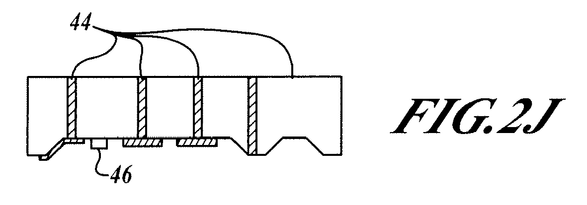
- a cap wafer 40 which is formed of Pyrex® or Si is etched with troughs 42 that will form an upper portion of cavities for housing the MEMS devices.
- the cap wafer 40 includes Si pins 44.
- a getter material 46 may be deposited into each of the troughs 42.
- the getter material may be bonded to the troughs 34 of the base substrate 30. Electrically conductive components may be applied on the base, sides, and around the tops of the troughs 42 (similar to FIGURES 2C-E).
- the cap wafer 40 of FIGURE 2J is inverted and attached to the device of FIGURE 2G such that the troughs 42 are co-located with the MEMS devices in the device layer 22 and the troughs 34 formed in the wafer 30.
- Bonding can be performed by any of the number of methods, such as anodic bonding, direct Si to Si, heat and pressure bonding (also called fusion bonding), eutectic bonding, frit bonding or some other method.
- the getter material 46 is activated by heating the device to a pre-defined temperature, such as 300°C. Activation of the getter material 46 results in a gettering in the cavity formed by the troughs 42 and 34. This bonding is very similar to the bond made from the device layer 22 to the first wafer 30.
- a Si pin 32 in the first wafer 30 may be bonded to a Si pin 44 in the wafter 40 via the device layer 22.
- the resulting device shown in FIGURE 2K now includes MEMS devices formed in vacuum cavities that are electrically connected to an external top and or bottom surface of the device via the Si pins 32 and 44. Therefore, the device can now be connected to a printed wiring board (PWB), using the Si pins 32 and 44. It is possible to connect the Si pins 32 directly to a printed circuit board, or to bring the signals out of the die in one pattern and then connect to the board using flip chip technique (if the pins are on the bottom) or wirebond technique (for pins on the top) using a different pattern. Therefore, traces are formed from the Si pins 32 and 44 to pads on other areas on the surface of the die.
- PWB printed wiring board
- the cap wafer 40 is a borosilicate glass wafer that does not include any Si pins, therefore all signals are sent through the pins of the first glass wafer 30.
- the cap wafer 40 may be a silicon wafer that is anodically or frit bonded to the first glass wafer 30 (ensuring hermiticity).
- FIGURES 2A-K are preferably performed across an entire wafer.
- a plurality of MEMS cavities are formed and once the cap wafer is bonded to the base wafer, then the entire wafer is diced in order to separate the cavities into definite units (individual die) for eventual attachment to a circuit board or other die such as an Application Specific Integrate Circuit (ASIC) die.
- ASIC Application Specific Integrate Circuit
Landscapes
- Engineering & Computer Science (AREA)
- Microelectronics & Electronic Packaging (AREA)
- Manufacturing & Machinery (AREA)
- Micromachines (AREA)
Abstract

Description
- Currently, Micro Electro-Mechanical Systems (MEMS) devices are packaged using chip scale packaging techniques, such as that shown in FIGURE 1. The MEMS device is first created on a substrate. The MEMS device and substrate are then placed within a housing with electrical leads that extend to and through the housing for electrically connecting the MEMS device with other systems external to the housing. This method incurs the extra cost of the housing materials as well as the time and cost of mounting the substrate and MEMS device within the housing in such a manner so as not to exhibit any thermal stress due to differences in coefficients of thermal expansion between the substrate and the housing. Also, the resulting device formed by current methods is a larger package that takes up a large amount real estate in the final integrated circuit product.
- Therefore, there exists a need in the art for lower cost methods for manufacturing wafer-level vacuum packaged devices.
- The present invention provides a vacuum package device and method of making a vacuum package device. The device includes a device layer having one or more Micro Electro-Mechanical Systems (MEMS) devices. The device layer includes one or more electrical leads coupled to the one or more MEMS devices. The device also includes a first wafer having one or more silicon pins, wherein a first surface of the first wafer is bonded to a first surface of the device layer in such a manner that the one or more silicon pins are in electrical communication with the electrical leads. A second wafer is bonded to a second surface of the device layer.
- The first and second wafers include one or more troughs that are co-located with the MEMS device to form one or more cavities. A getter material is deposited within at least one of the cavities and activated in order to create a vacuum within the respective cavity.
- The first wafer is formed of borosilicate glass (such as Pyrex® glass produced by Coming) and the second wafer is formed of silicon.
- The preferred and alternative embodiments of the present invention are described in detail below with reference to the following drawings:
- FIGURE 1 illustrates a side cut-away view of a hermetically packaged device formed in accordance with the prior art; and
- FIGURES 2A-K illustrate fabrication stages of a wafer-level vacuum package device formed in accordance with an embodiment of the present invention.
- FIGURES 2A-2K illustrate stages in a fabrication process for creating a wafer-level vacuum packaged device. First at FIGURES 2A and B, a
device layer wafer 20 is created by Deep Reactive Ion Etching of an epitaxial layer on a silicon substrate. Alternately, this device layer wafer 20 could be created by other surface and bulk silicon micromachining methods. Thedevice layer wafer 20 includes a mechanism ordevice layer 22 on top of asubstrate 24. The mechanism formed in this step is intentionally surrounded by a frame in the same layer to serve as a "seal ring" in a later step. - As shown in FIGURE 2C, a
first glass wafer 30 has one or more embeddedSi pins 32. Thewafer 30 is preferably a borosilicate glass wafer (such as Pyrex® glass produced by Corning). Thepins 32 are spaced apart on thewafer 30 at pre-defined distances in order to be proximate to a MEMS device electrical connection. Thepins 32 are embedded in thewafer 30 and are hermetically sealed with thewafer 30. Thepins 32 completely penetrate thewafer 30, and are finished to be flush with or very slightly proud of the surface of thewafer 30. As shown in FIGURE 2D,troughs 34 are etched into a top surface of thewafer 30 in order to form a cavity for housing (and providing a capacitive gap for) the MEMS device. As shown in FIGURE 2E, Electrical connection between the mechanism (MEMS device) and thepins 32 which run through thewafer 30 is made during this step, when metal traces and "pads" 36 (areas designated for later electrical connections) are deposited on the tops of thepins 32. The electrically conductive components, traces to the components, andpads 36 are designed to align therespective Si pins 32. Next, the device wafer 20 shown in FIGURE 2B is inverted and then attached to the top surface of thewafer 30 using any of the number of various bonding methods, such as an anodic wafer bonding for bonding Si and Pyrex®. Other methods that could be used include frit, eutectic, or adhesive bonding. Next, thesacrificial substrate 24 of thewafer 20 is removed by etching, thereby leaving just thedevice layer 22 attached to the top surface of thewafer 30. Prior to bonding, the device/mechanism of FIGURE 2B is positioned over thewafer 30 such that the MEMS device created in the device layer is co-located with atrough 34 where the MEMS device needs to be free to move. Thedevice layer 22 is attached to thefirst wafer 30 at connection points or mesas. Bonding brings the metal patterns on thefirst wafer 30 into intimate contact with the Silicon of thedevice layer 22, forming an electrical connection. These pads may be directly on top of thepins 32, or be connected by a metal trace on thefirst wafer 30 to a point where the metal is deposited on a pin. - Removal of the
substrate 24 is performed by any of a number of known substrate removal methods, such as buffing, etching, grinding, polishing, plasma etching (RIE, DRIE), ion milling, chemical etching (where the substrate is dissolved by the solution but the device layer is not, due to proper doping) such as KOH, EDP, TMAH etc., or other known methods. - As shown in FIGURES 2H-J, a
cap wafer 40 which is formed of Pyrex® or Si is etched withtroughs 42 that will form an upper portion of cavities for housing the MEMS devices. In this embodiment thecap wafer 40 includes Sipins 44. Agetter material 46 may be deposited into each of thetroughs 42. In an alternate embodiment, the getter material may be bonded to thetroughs 34 of thebase substrate 30. Electrically conductive components may be applied on the base, sides, and around the tops of the troughs 42 (similar to FIGURES 2C-E). - As shown in FIGURE 2K, the
cap wafer 40 of FIGURE 2J is inverted and attached to the device of FIGURE 2G such that thetroughs 42 are co-located with the MEMS devices in thedevice layer 22 and thetroughs 34 formed in thewafer 30. Bonding can be performed by any of the number of methods, such as anodic bonding, direct Si to Si, heat and pressure bonding (also called fusion bonding), eutectic bonding, frit bonding or some other method. At the time of the bonding of the cap wafer 40 to the base structure of FIGURE 2G (or after the bonding occurs), thegetter material 46 is activated by heating the device to a pre-defined temperature, such as 300°C. Activation of thegetter material 46 results in a gettering in the cavity formed by thetroughs device layer 22 to thefirst wafer 30. - In another embodiment, a
Si pin 32 in thefirst wafer 30 may be bonded to aSi pin 44 in thewafter 40 via thedevice layer 22. - The resulting device shown in FIGURE 2K now includes MEMS devices formed in vacuum cavities that are electrically connected to an external top and or bottom surface of the device via the
Si pins Si pins Si pins 32 directly to a printed circuit board, or to bring the signals out of the die in one pattern and then connect to the board using flip chip technique (if the pins are on the bottom) or wirebond technique (for pins on the top) using a different pattern. Therefore, traces are formed from theSi pins - In an alternate embodiment, the
cap wafer 40 is a borosilicate glass wafer that does not include any Si pins, therefore all signals are sent through the pins of thefirst glass wafer 30. Thecap wafer 40 may be a silicon wafer that is anodically or frit bonded to the first glass wafer 30 (ensuring hermiticity). - The processes shown above in FIGURES 2A-K are preferably performed across an entire wafer. In other words, a plurality of MEMS cavities are formed and once the cap wafer is bonded to the base wafer, then the entire wafer is diced in order to separate the cavities into definite units (individual die) for eventual attachment to a circuit board or other die such as an Application Specific Integrate Circuit (ASIC) die.
- While the preferred embodiment of the invention has been illustrated and described, as noted above, many changes can be made without departing from the spirit and scope of the invention. Accordingly, the scope of the invention is not limited by the disclosure of the preferred embodiment. Instead, the invention should be determined entirely by reference to the claims that follow.
- The embodiments of the invention in which an exclusive property or privilege is claimed are defined as follows:
Claims (10)
- A hermetically sealed device comprising:a device layer (22) comprising one or more Micro Electro-Mechanical Systems (MEMS) devices;a first wafer (30) includes borosilicate glass having one or more silicon pins (32), wherein a first surface of the first wafer with electrically active areas and leads is bonded to a first surface of the device layer in such a manner that the one or more silicon pins are in electrical communication with the electrical leads and/or individual sections of the MEMS device; anda second wafer (40) bonded to a second surface of the device layer.
- The device of Claim 1, wherein the first and second wafers include one or more troughs forming one or more cavities to contain one or more MEMS devices.
- The device of Claim 2, further comprising a getter material (46) deposited within one or more of the cavities, wherein the getter material is deposited in one or both of the first and second wafers' troughs prior to bonding the wafers to the device layer and the getter material being activated using a heating process.
- The device of Claim 1, wherein the second wafer includes one or more silicon pins, wherein the second wafer includes first and second surfaces, the one or more silicon pins extending from the first surface to the second surface.
- The device of Claim 1, wherein the first wafer includes a second surface opposite the first surface, the silicon pins extending from the first surface to the second surface.
- A method of making a vacuum package device, the method comprising:forming one or more Micro Electro-Mechanical Systems (MEMS) devices in a device layer;forming a first wafer having one or more silicon pins and one or more electrical leads coupled to the silicon pins;bonding the first wafer having the one or more silicon pins to a first surface of the device layer in such a manner that the one or more silicon pins are in electrical communication with portions of the device layer; andbonding a second wafer formed in a manner similar to the first wafer to a second surface of the device layer to form a seal.
- The method of Claim 6, further comprising forming one or more troughs in the first and second wafers.
- The method of Claim 7, further comprising positioning the troughs over the one or more MEMS devices to form a cavity.
- The method of Claim 7, further comprising depositing a getter material within at least one of the troughs as required, further comprising heating the getter material to an activation point.
- The method of Claim 6, wherein the first and second wafer includes Pyrex glass and the device wafer includes silicon.
Applications Claiming Priority (1)
| Application Number | Priority Date | Filing Date | Title |
|---|---|---|---|
| US11/462,767 US7402905B2 (en) | 2006-08-07 | 2006-08-07 | Methods of fabrication of wafer-level vacuum packaged devices |
Publications (3)
| Publication Number | Publication Date |
|---|---|
| EP1886969A2 true EP1886969A2 (en) | 2008-02-13 |
| EP1886969A3 EP1886969A3 (en) | 2009-11-04 |
| EP1886969B1 EP1886969B1 (en) | 2012-04-18 |
Family
ID=38516123
Family Applications (1)
| Application Number | Title | Priority Date | Filing Date |
|---|---|---|---|
| EP07113745A Active EP1886969B1 (en) | 2006-08-07 | 2007-08-02 | Methods of fabrication of wafer-level vacuum packaged devices |
Country Status (3)
| Country | Link |
|---|---|
| US (1) | US7402905B2 (en) |
| EP (1) | EP1886969B1 (en) |
| JP (1) | JP2008132587A (en) |
Cited By (6)
| Publication number | Priority date | Publication date | Assignee | Title |
|---|---|---|---|---|
| GB2451921A (en) * | 2007-08-17 | 2009-02-18 | Wolfson Microelectronics Plc | MEMS package |
| GB2451908A (en) * | 2007-08-17 | 2009-02-18 | Wolfson Microelectronics Plc | MEMS microphone package |
| CN102079502A (en) * | 2010-12-03 | 2011-06-01 | 华东光电集成器件研究所 | MEMS (micro electro mechanical system) device and wafer-level vacuum packaging method thereof |
| CN101439843B (en) * | 2008-10-10 | 2011-08-31 | 北京大学 | Miniature atomic air chamber encapsulation technology |
| CN103503137A (en) * | 2011-05-09 | 2014-01-08 | 惠普发展公司,有限责任合伙企业 | Bonded wafer structures |
| CN105668501A (en) * | 2016-01-28 | 2016-06-15 | 安徽北方芯动联科微系统技术有限公司 | Chip scale packaged MEMS (Micro-Electro-Mechanical Systems) chip with multifunctional cover board and manufacturing method of chip scale packaged MEMS chip with multifunctional cover board |
Families Citing this family (18)
| Publication number | Priority date | Publication date | Assignee | Title |
|---|---|---|---|---|
| US20100084752A1 (en) * | 2008-10-08 | 2010-04-08 | Honeywell International Inc. | Systems and methods for implementing a wafer level hermetic interface chip |
| US7955885B1 (en) | 2009-01-09 | 2011-06-07 | Integrated Device Technology, Inc. | Methods of forming packaged micro-electromechanical devices |
| DE102009002485A1 (en) * | 2009-04-20 | 2010-10-21 | Robert Bosch Gmbh | Method of making capped MEMS devices |
| US20100320595A1 (en) * | 2009-06-22 | 2010-12-23 | Honeywell International Inc. | Hybrid hermetic interface chip |
| JP2011218462A (en) | 2010-04-06 | 2011-11-04 | Seiko Epson Corp | Mems device |
| EP2514713B1 (en) * | 2011-04-20 | 2013-10-02 | Tronics Microsystems S.A. | A micro-electromechanical system (MEMS) device |
| US9045332B2 (en) * | 2011-11-29 | 2015-06-02 | Qualcomm Mems Technologies, Inc. | Thin back glass interconnect |
| SE537869C2 (en) * | 2012-11-01 | 2015-11-03 | Silex Microsystems Ab | Substrate-through vior |
| EP2736071B8 (en) | 2012-11-22 | 2017-04-19 | Tronic's Microsystems S.A. | Wafer level package with getter |
| US10273147B2 (en) | 2013-07-08 | 2019-04-30 | Motion Engine Inc. | MEMS components and method of wafer-level manufacturing thereof |
| JP6339669B2 (en) * | 2013-07-08 | 2018-06-06 | モーション・エンジン・インコーポレーテッド | MEMS device and method of manufacturing |
| EP3028007A4 (en) | 2013-08-02 | 2017-07-12 | Motion Engine Inc. | Mems motion sensor and method of manufacturing |
| WO2015154173A1 (en) | 2014-04-10 | 2015-10-15 | Motion Engine Inc. | Mems pressure sensor |
| WO2015184531A1 (en) * | 2014-06-02 | 2015-12-10 | Motion Engine Inc. | Multi-mass mems motion sensor |
| US9688529B2 (en) * | 2014-06-10 | 2017-06-27 | Qorvo Us, Inc. | Glass wafer assembly |
| CA3004760A1 (en) | 2014-12-09 | 2016-06-16 | Motion Engine Inc. | 3d mems magnetometer and associated methods |
| WO2016112463A1 (en) | 2015-01-15 | 2016-07-21 | Motion Engine Inc. | 3d mems device with hermetic cavity |
| EP4385944A1 (en) * | 2022-12-14 | 2024-06-19 | Imec VZW | A method for bonding and interconnecting micro-electronic components |
Citations (1)
| Publication number | Priority date | Publication date | Assignee | Title |
|---|---|---|---|---|
| EP0369352A1 (en) | 1988-11-15 | 1990-05-23 | Hitachi, Ltd. | Capacitance type accelerometer and method of manufacturing the same |
Family Cites Families (13)
| Publication number | Priority date | Publication date | Assignee | Title |
|---|---|---|---|---|
| US6143583A (en) * | 1998-06-08 | 2000-11-07 | Honeywell, Inc. | Dissolved wafer fabrication process and associated microelectromechanical device having a support substrate with spacing mesas |
| JP2000186931A (en) * | 1998-12-21 | 2000-07-04 | Murata Mfg Co Ltd | Small-sized electronic component and its manufacture, and via hole forming method for the small-sized electronic component |
| JP3771100B2 (en) * | 2000-01-19 | 2006-04-26 | アルプス電気株式会社 | Capacitance detection type sensor, gyroscope and input device |
| US7049175B2 (en) * | 2001-11-07 | 2006-05-23 | Board Of Trustees Of The University Of Arkansas | Method of packaging RF MEMS |
| JP4223246B2 (en) * | 2002-08-08 | 2009-02-12 | 富士通コンポーネント株式会社 | Micro relay and manufacturing method thereof |
| WO2004030057A1 (en) * | 2002-09-06 | 2004-04-08 | Fraunhofer Gesellschaft Zur Förderung Der Angewandten Forschung E. V. | Glass-type planar substrate, use thereof, and method for the production thereof |
| US7554136B2 (en) * | 2002-09-13 | 2009-06-30 | Advantest Corporation | Micro-switch device and method for manufacturing the same |
| ITMI20030069A1 (en) * | 2003-01-17 | 2004-07-18 | Getters Spa | MICROMECHANICAL OR MICROOPTOELECTRONIC DEVICES WITH STORAGE OF GETTER MATERIAL AND INTEGRATED HEATER. |
| US20050085053A1 (en) * | 2003-10-20 | 2005-04-21 | Chien-Hua Chen | Method of activating a getter structure |
| US6936918B2 (en) * | 2003-12-15 | 2005-08-30 | Analog Devices, Inc. | MEMS device with conductive path through substrate |
| US6949807B2 (en) * | 2003-12-24 | 2005-09-27 | Honeywell International, Inc. | Signal routing in a hermetically sealed MEMS device |
| US7153759B2 (en) * | 2004-04-20 | 2006-12-26 | Agency For Science Technology And Research | Method of fabricating microelectromechanical system structures |
| US8043880B2 (en) * | 2005-07-28 | 2011-10-25 | Hewlett-Packard Development, L.P. | Microelectronic device |
-
2006
- 2006-08-07 US US11/462,767 patent/US7402905B2/en active Active
-
2007
- 2007-08-02 EP EP07113745A patent/EP1886969B1/en active Active
- 2007-08-06 JP JP2007204178A patent/JP2008132587A/en active Pending
Patent Citations (1)
| Publication number | Priority date | Publication date | Assignee | Title |
|---|---|---|---|---|
| EP0369352A1 (en) | 1988-11-15 | 1990-05-23 | Hitachi, Ltd. | Capacitance type accelerometer and method of manufacturing the same |
Cited By (10)
| Publication number | Priority date | Publication date | Assignee | Title |
|---|---|---|---|---|
| GB2451921A (en) * | 2007-08-17 | 2009-02-18 | Wolfson Microelectronics Plc | MEMS package |
| GB2451908A (en) * | 2007-08-17 | 2009-02-18 | Wolfson Microelectronics Plc | MEMS microphone package |
| GB2451908B (en) * | 2007-08-17 | 2009-12-02 | Wolfson Microelectronics Plc | Mems package |
| CN101439843B (en) * | 2008-10-10 | 2011-08-31 | 北京大学 | Miniature atomic air chamber encapsulation technology |
| CN102079502A (en) * | 2010-12-03 | 2011-06-01 | 华东光电集成器件研究所 | MEMS (micro electro mechanical system) device and wafer-level vacuum packaging method thereof |
| CN102079502B (en) * | 2010-12-03 | 2014-08-13 | 华东光电集成器件研究所 | MEMS (micro electro mechanical system) device and wafer-level vacuum packaging method thereof |
| CN103503137A (en) * | 2011-05-09 | 2014-01-08 | 惠普发展公司,有限责任合伙企业 | Bonded wafer structures |
| EP2707899A4 (en) * | 2011-05-09 | 2014-11-05 | Hewlett Packard Development Co | BONDED PLATELET STRUCTURES |
| CN103503137B (en) * | 2011-05-09 | 2016-04-13 | 惠普发展公司,有限责任合伙企业 | The chip architecture of bonding |
| CN105668501A (en) * | 2016-01-28 | 2016-06-15 | 安徽北方芯动联科微系统技术有限公司 | Chip scale packaged MEMS (Micro-Electro-Mechanical Systems) chip with multifunctional cover board and manufacturing method of chip scale packaged MEMS chip with multifunctional cover board |
Also Published As
| Publication number | Publication date |
|---|---|
| EP1886969A3 (en) | 2009-11-04 |
| JP2008132587A (en) | 2008-06-12 |
| EP1886969B1 (en) | 2012-04-18 |
| US7402905B2 (en) | 2008-07-22 |
| US20080029863A1 (en) | 2008-02-07 |
Similar Documents
| Publication | Publication Date | Title |
|---|---|---|
| EP1886969B1 (en) | Methods of fabrication of wafer-level vacuum packaged devices | |
| US8476737B2 (en) | Environment-resistant module, micropackage and methods of manufacturing same | |
| EP2121511B1 (en) | Method of packaging an electronic or micromechanical component | |
| CN102381678B (en) | MEMS device assembly and method for packing thereof | |
| EP3394586B1 (en) | Stress-isolated absolute pressure sensor | |
| US8476087B2 (en) | Methods for fabricating sensor device package using a sealing structure | |
| US20050205951A1 (en) | Flip chip bonded micro-electromechanical system (MEMS) device | |
| US20170089783A1 (en) | Various stress free sensor packages using wafer level supporting die and air gap technique | |
| US20120266684A1 (en) | Sensor device with sealing structure | |
| JP2010514180A (en) | Encapsulation module, method for its generation and use thereof | |
| US10266392B2 (en) | Environment-resistant module, micropackage and methods of manufacturing same | |
| EP2246292B1 (en) | Package interface plate for mechanical isolation of MEMS structures | |
| JP2009516598A (en) | Method for producing microelectromechanical component and microelectromechanical component | |
| US20050054133A1 (en) | Wafer level capped sensor | |
| US9073750B2 (en) | Manufacturing method of micro-electro-mechanical system device and micro-electro-mechanical system device made thereby | |
| JP2013154465A (en) | Mems device assembly and method of packaging the same | |
| EP2266920A2 (en) | Interface lid for hermetic MEMS package | |
| WO2016200346A1 (en) | Hermetic packaging method for soi-mems devices with embedded vertical feedthroughs | |
| CN105189337B (en) | Microelectromechanical device and manufacturing method | |
| US20230406697A1 (en) | Production method for a micromechanical sensor apparatus, and corresponding micromechanical sensor apparatus | |
| US7436076B2 (en) | Micromechanical component having an anodically bonded cap and a manufacturing method | |
| US20160146850A1 (en) | Micromechanical sensor device and corresponding manufacturing method | |
| CN107986229B (en) | Opening device of micro-electro-mechanical device and preparation multiplexing method thereof | |
| JP2011204950A (en) | Metal embedded glass substrate and method of manufacturing the same, and mems device | |
| Chiao et al. | Introduction to MEMS packaging |
Legal Events
| Date | Code | Title | Description |
|---|---|---|---|
| PUAI | Public reference made under article 153(3) epc to a published international application that has entered the european phase |
Free format text: ORIGINAL CODE: 0009012 |
|
| AK | Designated contracting states |
Kind code of ref document: A2 Designated state(s): AT BE BG CH CY CZ DE DK EE ES FI FR GB GR HU IE IS IT LI LT LU LV MC MT NL PL PT RO SE SI SK TR |
|
| AX | Request for extension of the european patent |
Extension state: AL BA HR MK YU |
|
| PUAL | Search report despatched |
Free format text: ORIGINAL CODE: 0009013 |
|
| AK | Designated contracting states |
Kind code of ref document: A3 Designated state(s): AT BE BG CH CY CZ DE DK EE ES FI FR GB GR HU IE IS IT LI LT LU LV MC MT NL PL PT RO SE SI SK TR |
|
| AX | Request for extension of the european patent |
Extension state: AL BA HR MK RS |
|
| 17P | Request for examination filed |
Effective date: 20100329 |
|
| 17Q | First examination report despatched |
Effective date: 20100423 |
|
| AKX | Designation fees paid |
Designated state(s): DE FR GB |
|
| GRAP | Despatch of communication of intention to grant a patent |
Free format text: ORIGINAL CODE: EPIDOSNIGR1 |
|
| GRAS | Grant fee paid |
Free format text: ORIGINAL CODE: EPIDOSNIGR3 |
|
| GRAA | (expected) grant |
Free format text: ORIGINAL CODE: 0009210 |
|
| AK | Designated contracting states |
Kind code of ref document: B1 Designated state(s): DE FR GB |
|
| RAP1 | Party data changed (applicant data changed or rights of an application transferred) |
Owner name: HONEYWELL INTERNATIONAL INC. |
|
| REG | Reference to a national code |
Ref country code: GB Ref legal event code: FG4D |
|
| REG | Reference to a national code |
Ref country code: DE Ref legal event code: R096 Ref document number: 602007022061 Country of ref document: DE Effective date: 20120614 |
|
| PLBE | No opposition filed within time limit |
Free format text: ORIGINAL CODE: 0009261 |
|
| STAA | Information on the status of an ep patent application or granted ep patent |
Free format text: STATUS: NO OPPOSITION FILED WITHIN TIME LIMIT |
|
| 26N | No opposition filed |
Effective date: 20130121 |
|
| REG | Reference to a national code |
Ref country code: DE Ref legal event code: R097 Ref document number: 602007022061 Country of ref document: DE Effective date: 20130121 |
|
| REG | Reference to a national code |
Ref country code: FR Ref legal event code: PLFP Year of fee payment: 10 |
|
| PGFP | Annual fee paid to national office [announced via postgrant information from national office to epo] |
Ref country code: DE Payment date: 20160831 Year of fee payment: 10 Ref country code: GB Payment date: 20160725 Year of fee payment: 10 |
|
| REG | Reference to a national code |
Ref country code: FR Ref legal event code: PLFP Year of fee payment: 11 |
|
| REG | Reference to a national code |
Ref country code: DE Ref legal event code: R119 Ref document number: 602007022061 Country of ref document: DE |
|
| GBPC | Gb: european patent ceased through non-payment of renewal fee |
Effective date: 20170802 |
|
| PG25 | Lapsed in a contracting state [announced via postgrant information from national office to epo] |
Ref country code: DE Free format text: LAPSE BECAUSE OF NON-PAYMENT OF DUE FEES Effective date: 20180301 Ref country code: GB Free format text: LAPSE BECAUSE OF NON-PAYMENT OF DUE FEES Effective date: 20170802 |
|
| REG | Reference to a national code |
Ref country code: FR Ref legal event code: PLFP Year of fee payment: 12 |
|
| P01 | Opt-out of the competence of the unified patent court (upc) registered |
Effective date: 20230525 |
|
| PGFP | Annual fee paid to national office [announced via postgrant information from national office to epo] |
Ref country code: FR Payment date: 20250825 Year of fee payment: 19 |