EP1535978B1 - Polishing cloth and method of manufacturing semiconductor device - Google Patents
Polishing cloth and method of manufacturing semiconductor device Download PDFInfo
- Publication number
- EP1535978B1 EP1535978B1 EP04027989A EP04027989A EP1535978B1 EP 1535978 B1 EP1535978 B1 EP 1535978B1 EP 04027989 A EP04027989 A EP 04027989A EP 04027989 A EP04027989 A EP 04027989A EP 1535978 B1 EP1535978 B1 EP 1535978B1
- Authority
- EP
- European Patent Office
- Prior art keywords
- meth
- polishing
- koh
- semiconductor device
- molded body
- Prior art date
- Legal status (The legal status is an assumption and is not a legal conclusion. Google has not performed a legal analysis and makes no representation as to the accuracy of the status listed.)
- Expired - Lifetime
Links
- 238000005498 polishing Methods 0.000 title claims description 356
- 239000004744 fabric Substances 0.000 title claims description 156
- 239000004065 semiconductor Substances 0.000 title claims description 96
- 238000004519 manufacturing process Methods 0.000 title claims description 52
- 239000010410 layer Substances 0.000 claims description 76
- 229920001577 copolymer Polymers 0.000 claims description 75
- 229920006243 acrylic copolymer Polymers 0.000 claims description 56
- VYPSYNLAJGMNEJ-UHFFFAOYSA-N Silicium dioxide Chemical compound O=[Si]=O VYPSYNLAJGMNEJ-UHFFFAOYSA-N 0.000 claims description 55
- 239000002253 acid Substances 0.000 claims description 53
- 239000002002 slurry Substances 0.000 claims description 49
- 125000002887 hydroxy group Chemical group [H]O* 0.000 claims description 45
- 239000006061 abrasive grain Substances 0.000 claims description 40
- 239000000758 substrate Substances 0.000 claims description 40
- 239000011229 interlayer Substances 0.000 claims description 36
- 239000000463 material Substances 0.000 claims description 36
- 239000000178 monomer Substances 0.000 claims description 35
- 239000004020 conductor Substances 0.000 claims description 29
- 239000010949 copper Substances 0.000 claims description 28
- CERQOIWHTDAKMF-UHFFFAOYSA-N Methacrylic acid Chemical compound CC(=C)C(O)=O CERQOIWHTDAKMF-UHFFFAOYSA-N 0.000 claims description 25
- RYGMFSIKBFXOCR-UHFFFAOYSA-N Copper Chemical compound [Cu] RYGMFSIKBFXOCR-UHFFFAOYSA-N 0.000 claims description 21
- 229910052802 copper Inorganic materials 0.000 claims description 21
- 239000000377 silicon dioxide Substances 0.000 claims description 20
- -1 (meth)acrylic acid hydroxyalkyl ester Chemical class 0.000 claims description 16
- 125000000217 alkyl group Chemical group 0.000 claims description 14
- 125000004432 carbon atom Chemical group C* 0.000 claims description 12
- 230000015572 biosynthetic process Effects 0.000 claims description 11
- 229910000881 Cu alloy Inorganic materials 0.000 claims description 10
- 230000004888 barrier function Effects 0.000 claims description 10
- 230000001788 irregular Effects 0.000 claims description 10
- 229910000420 cerium oxide Inorganic materials 0.000 claims description 8
- 229920001971 elastomer Polymers 0.000 claims description 8
- BMMGVYCKOGBVEV-UHFFFAOYSA-N oxo(oxoceriooxy)cerium Chemical compound [Ce]=O.O=[Ce]=O BMMGVYCKOGBVEV-UHFFFAOYSA-N 0.000 claims description 8
- 125000002496 methyl group Chemical group [H]C([H])([H])* 0.000 claims description 7
- 239000000126 substance Substances 0.000 claims description 7
- 125000000954 2-hydroxyethyl group Chemical group [H]C([*])([H])C([H])([H])O[H] 0.000 claims description 6
- NIXOWILDQLNWCW-UHFFFAOYSA-M Acrylate Chemical compound [O-]C(=O)C=C NIXOWILDQLNWCW-UHFFFAOYSA-M 0.000 claims description 6
- 125000002947 alkylene group Chemical group 0.000 claims description 5
- 125000004435 hydrogen atom Chemical group [H]* 0.000 claims description 5
- KWYUFKZDYYNOTN-UHFFFAOYSA-M Potassium hydroxide Chemical compound [OH-].[K+] KWYUFKZDYYNOTN-UHFFFAOYSA-M 0.000 description 129
- 235000012431 wafers Nutrition 0.000 description 44
- XUIMIQQOPSSXEZ-UHFFFAOYSA-N Silicon Chemical compound [Si] XUIMIQQOPSSXEZ-UHFFFAOYSA-N 0.000 description 34
- 229910052710 silicon Inorganic materials 0.000 description 34
- 239000010703 silicon Substances 0.000 description 34
- XLYOFNOQVPJJNP-UHFFFAOYSA-N water Substances O XLYOFNOQVPJJNP-UHFFFAOYSA-N 0.000 description 26
- 238000000034 method Methods 0.000 description 23
- SOGAXMICEFXMKE-UHFFFAOYSA-N Butylmethacrylate Chemical compound CCCCOC(=O)C(C)=C SOGAXMICEFXMKE-UHFFFAOYSA-N 0.000 description 22
- 150000007524 organic acids Chemical class 0.000 description 21
- 230000000052 comparative effect Effects 0.000 description 19
- 239000007864 aqueous solution Substances 0.000 description 14
- 229910052681 coesite Inorganic materials 0.000 description 13
- 229910052906 cristobalite Inorganic materials 0.000 description 13
- 238000005342 ion exchange Methods 0.000 description 13
- 239000000203 mixture Substances 0.000 description 13
- 229910052682 stishovite Inorganic materials 0.000 description 13
- 229910052905 tridymite Inorganic materials 0.000 description 13
- 229910052814 silicon oxide Inorganic materials 0.000 description 12
- 239000000243 solution Substances 0.000 description 11
- WOBHKFSMXKNTIM-UHFFFAOYSA-N Hydroxyethyl methacrylate Chemical compound CC(=C)C(=O)OCCO WOBHKFSMXKNTIM-UHFFFAOYSA-N 0.000 description 10
- 229910052751 metal Inorganic materials 0.000 description 10
- 239000002184 metal Substances 0.000 description 10
- VVQNEPGJFQJSBK-UHFFFAOYSA-N Methyl methacrylate Chemical compound COC(=O)C(C)=C VVQNEPGJFQJSBK-UHFFFAOYSA-N 0.000 description 9
- 229910045601 alloy Inorganic materials 0.000 description 9
- 239000000956 alloy Substances 0.000 description 9
- 238000006243 chemical reaction Methods 0.000 description 9
- 230000000977 initiatory effect Effects 0.000 description 9
- 238000006116 polymerization reaction Methods 0.000 description 9
- OZAIFHULBGXAKX-UHFFFAOYSA-N 2-(2-cyanopropan-2-yldiazenyl)-2-methylpropanenitrile Chemical compound N#CC(C)(C)N=NC(C)(C)C#N OZAIFHULBGXAKX-UHFFFAOYSA-N 0.000 description 8
- 229910052581 Si3N4 Inorganic materials 0.000 description 8
- 239000007800 oxidant agent Substances 0.000 description 8
- HQVNEWCFYHHQES-UHFFFAOYSA-N silicon nitride Chemical compound N12[Si]34N5[Si]62N3[Si]51N64 HQVNEWCFYHHQES-UHFFFAOYSA-N 0.000 description 8
- IJGRMHOSHXDMSA-UHFFFAOYSA-N Atomic nitrogen Chemical compound N#N IJGRMHOSHXDMSA-UHFFFAOYSA-N 0.000 description 7
- 229910001873 dinitrogen Inorganic materials 0.000 description 7
- 238000000465 moulding Methods 0.000 description 7
- NIXOWILDQLNWCW-UHFFFAOYSA-N acrylic acid group Chemical group C(C=C)(=O)O NIXOWILDQLNWCW-UHFFFAOYSA-N 0.000 description 6
- 239000003795 chemical substances by application Substances 0.000 description 6
- 238000010276 construction Methods 0.000 description 6
- JVTAAEKCZFNVCJ-UHFFFAOYSA-N lactic acid Chemical compound CC(O)C(O)=O JVTAAEKCZFNVCJ-UHFFFAOYSA-N 0.000 description 6
- 238000003756 stirring Methods 0.000 description 6
- PNEYBMLMFCGWSK-UHFFFAOYSA-N aluminium oxide Inorganic materials [O-2].[O-2].[O-2].[Al+3].[Al+3] PNEYBMLMFCGWSK-UHFFFAOYSA-N 0.000 description 5
- 125000003178 carboxy group Chemical group [H]OC(*)=O 0.000 description 5
- 238000005229 chemical vapour deposition Methods 0.000 description 5
- 238000007334 copolymerization reaction Methods 0.000 description 5
- 238000001035 drying Methods 0.000 description 5
- 230000001747 exhibiting effect Effects 0.000 description 5
- 238000001746 injection moulding Methods 0.000 description 5
- 239000002245 particle Substances 0.000 description 5
- 229910052721 tungsten Inorganic materials 0.000 description 5
- 229920005830 Polyurethane Foam Polymers 0.000 description 4
- 238000005530 etching Methods 0.000 description 4
- 239000007789 gas Substances 0.000 description 4
- 239000011521 glass Substances 0.000 description 4
- 239000011496 polyurethane foam Substances 0.000 description 4
- 238000010992 reflux Methods 0.000 description 4
- SMZOUWXMTYCWNB-UHFFFAOYSA-N 2-(2-methoxy-5-methylphenyl)ethanamine Chemical compound COC1=CC=C(C)C=C1CCN SMZOUWXMTYCWNB-UHFFFAOYSA-N 0.000 description 3
- 229910021364 Al-Si alloy Inorganic materials 0.000 description 3
- MHAJPDPJQMAIIY-UHFFFAOYSA-N Hydrogen peroxide Chemical compound OO MHAJPDPJQMAIIY-UHFFFAOYSA-N 0.000 description 3
- CTQNGGLPUBDAKN-UHFFFAOYSA-N O-Xylene Chemical compound CC1=CC=CC=C1C CTQNGGLPUBDAKN-UHFFFAOYSA-N 0.000 description 3
- 239000002202 Polyethylene glycol Substances 0.000 description 3
- BOTDANWDWHJENH-UHFFFAOYSA-N Tetraethyl orthosilicate Chemical compound CCO[Si](OCC)(OCC)OCC BOTDANWDWHJENH-UHFFFAOYSA-N 0.000 description 3
- 239000002801 charged material Substances 0.000 description 3
- 239000011248 coating agent Substances 0.000 description 3
- 238000000576 coating method Methods 0.000 description 3
- 230000003750 conditioning effect Effects 0.000 description 3
- 150000004699 copper complex Chemical class 0.000 description 3
- 229910003460 diamond Inorganic materials 0.000 description 3
- 239000010432 diamond Substances 0.000 description 3
- 238000009792 diffusion process Methods 0.000 description 3
- 238000007598 dipping method Methods 0.000 description 3
- 239000004310 lactic acid Substances 0.000 description 3
- 235000014655 lactic acid Nutrition 0.000 description 3
- 239000007788 liquid Substances 0.000 description 3
- 239000003973 paint Substances 0.000 description 3
- 238000001020 plasma etching Methods 0.000 description 3
- 229920001223 polyethylene glycol Polymers 0.000 description 3
- 238000007790 scraping Methods 0.000 description 3
- 239000007787 solid Substances 0.000 description 3
- 230000002522 swelling effect Effects 0.000 description 3
- WFKWXMTUELFFGS-UHFFFAOYSA-N tungsten Chemical compound [W] WFKWXMTUELFFGS-UHFFFAOYSA-N 0.000 description 3
- 239000010937 tungsten Substances 0.000 description 3
- 238000007740 vapor deposition Methods 0.000 description 3
- 239000002699 waste material Substances 0.000 description 3
- 239000008096 xylene Substances 0.000 description 3
- KDGNCLDCOVTOCS-UHFFFAOYSA-N (2-methylpropan-2-yl)oxy propan-2-yl carbonate Chemical compound CC(C)OC(=O)OOC(C)(C)C KDGNCLDCOVTOCS-UHFFFAOYSA-N 0.000 description 2
- ARXJGSRGQADJSQ-UHFFFAOYSA-N 1-methoxypropan-2-ol Chemical compound COCC(C)O ARXJGSRGQADJSQ-UHFFFAOYSA-N 0.000 description 2
- IEVADDDOVGMCSI-UHFFFAOYSA-N 2-hydroxybutyl 2-methylprop-2-enoate Chemical compound CCC(O)COC(=O)C(C)=C IEVADDDOVGMCSI-UHFFFAOYSA-N 0.000 description 2
- OMIGHNLMNHATMP-UHFFFAOYSA-N 2-hydroxyethyl prop-2-enoate Chemical compound OCCOC(=O)C=C OMIGHNLMNHATMP-UHFFFAOYSA-N 0.000 description 2
- GNSFRPWPOGYVLO-UHFFFAOYSA-N 3-hydroxypropyl 2-methylprop-2-enoate Chemical compound CC(=C)C(=O)OCCCO GNSFRPWPOGYVLO-UHFFFAOYSA-N 0.000 description 2
- QZPSOSOOLFHYRR-UHFFFAOYSA-N 3-hydroxypropyl prop-2-enoate Chemical compound OCCCOC(=O)C=C QZPSOSOOLFHYRR-UHFFFAOYSA-N 0.000 description 2
- NDWUBGAGUCISDV-UHFFFAOYSA-N 4-hydroxybutyl prop-2-enoate Chemical compound OCCCCOC(=O)C=C NDWUBGAGUCISDV-UHFFFAOYSA-N 0.000 description 2
- OZAIFHULBGXAKX-VAWYXSNFSA-N AIBN Substances N#CC(C)(C)\N=N\C(C)(C)C#N OZAIFHULBGXAKX-VAWYXSNFSA-N 0.000 description 2
- VZCYOOQTPOCHFL-OWOJBTEDSA-N Fumaric acid Chemical compound OC(=O)\C=C\C(O)=O VZCYOOQTPOCHFL-OWOJBTEDSA-N 0.000 description 2
- 239000004372 Polyvinyl alcohol Substances 0.000 description 2
- BLRPTPMANUNPDV-UHFFFAOYSA-N Silane Chemical compound [SiH4] BLRPTPMANUNPDV-UHFFFAOYSA-N 0.000 description 2
- MCMNRKCIXSYSNV-UHFFFAOYSA-N Zirconium dioxide Chemical compound O=[Zr]=O MCMNRKCIXSYSNV-UHFFFAOYSA-N 0.000 description 2
- 239000005380 borophosphosilicate glass Substances 0.000 description 2
- 150000001875 compounds Chemical class 0.000 description 2
- PTVDYARBVCBHSL-UHFFFAOYSA-N copper;hydrate Chemical compound O.[Cu] PTVDYARBVCBHSL-UHFFFAOYSA-N 0.000 description 2
- 125000000113 cyclohexyl group Chemical group [H]C1([H])C([H])([H])C([H])([H])C([H])(*)C([H])([H])C1([H])[H] 0.000 description 2
- 239000002270 dispersing agent Substances 0.000 description 2
- 150000002148 esters Chemical class 0.000 description 2
- 125000001495 ethyl group Chemical group [H]C([H])([H])C([H])([H])* 0.000 description 2
- 238000011156 evaluation Methods 0.000 description 2
- AMWRITDGCCNYAT-UHFFFAOYSA-L hydroxy(oxo)manganese;manganese Chemical compound [Mn].O[Mn]=O.O[Mn]=O AMWRITDGCCNYAT-UHFFFAOYSA-L 0.000 description 2
- 239000011810 insulating material Substances 0.000 description 2
- 125000000959 isobutyl group Chemical group [H]C([H])([H])C([H])(C([H])([H])[H])C([H])([H])* 0.000 description 2
- 125000001972 isopentyl group Chemical group [H]C([H])([H])C([H])(C([H])([H])[H])C([H])([H])C([H])([H])* 0.000 description 2
- 125000001449 isopropyl group Chemical group [H]C([H])([H])C([H])(*)C([H])([H])[H] 0.000 description 2
- 238000002844 melting Methods 0.000 description 2
- 230000008018 melting Effects 0.000 description 2
- 125000004108 n-butyl group Chemical group [H]C([H])([H])C([H])([H])C([H])([H])C([H])([H])* 0.000 description 2
- 125000001280 n-hexyl group Chemical group C(CCCCC)* 0.000 description 2
- 125000000740 n-pentyl group Chemical group [H]C([H])([H])C([H])([H])C([H])([H])C([H])([H])C([H])([H])* 0.000 description 2
- 125000004123 n-propyl group Chemical group [H]C([H])([H])C([H])([H])C([H])([H])* 0.000 description 2
- 235000005985 organic acids Nutrition 0.000 description 2
- 229920001515 polyalkylene glycol Polymers 0.000 description 2
- 229910021420 polycrystalline silicon Inorganic materials 0.000 description 2
- 229920000642 polymer Polymers 0.000 description 2
- 239000002685 polymerization catalyst Substances 0.000 description 2
- 230000000379 polymerizing effect Effects 0.000 description 2
- 229920002451 polyvinyl alcohol Polymers 0.000 description 2
- 239000000843 powder Substances 0.000 description 2
- LLHKCFNBLRBOGN-UHFFFAOYSA-N propylene glycol methyl ether acetate Chemical compound COCC(C)OC(C)=O LLHKCFNBLRBOGN-UHFFFAOYSA-N 0.000 description 2
- UBDIMPWXBMWVTC-UHFFFAOYSA-N quinoline-2-carboxylic acid Chemical compound C1=CC=CC2=NC(C(=O)O)=CC=C21.C1=CC=CC2=NC(C(=O)O)=CC=C21 UBDIMPWXBMWVTC-UHFFFAOYSA-N 0.000 description 2
- 239000011541 reaction mixture Substances 0.000 description 2
- 239000011347 resin Substances 0.000 description 2
- 229920005989 resin Polymers 0.000 description 2
- 125000002914 sec-butyl group Chemical group [H]C([H])([H])C([H])([H])C([H])(*)C([H])([H])[H] 0.000 description 2
- 229910000077 silane Inorganic materials 0.000 description 2
- SUKJFIGYRHOWBL-UHFFFAOYSA-N sodium hypochlorite Chemical compound [Na+].Cl[O-] SUKJFIGYRHOWBL-UHFFFAOYSA-N 0.000 description 2
- 239000002904 solvent Substances 0.000 description 2
- 239000004094 surface-active agent Substances 0.000 description 2
- 229910052719 titanium Inorganic materials 0.000 description 2
- VZCYOOQTPOCHFL-UHFFFAOYSA-N trans-butenedioic acid Natural products OC(=O)C=CC(O)=O VZCYOOQTPOCHFL-UHFFFAOYSA-N 0.000 description 2
- 125000000391 vinyl group Chemical group [H]C([*])=C([H])[H] 0.000 description 2
- 229920002554 vinyl polymer Polymers 0.000 description 2
- FVQMJJQUGGVLEP-UHFFFAOYSA-N (2-methylpropan-2-yl)oxy 2-ethylhexaneperoxoate Chemical compound CCCCC(CC)C(=O)OOOC(C)(C)C FVQMJJQUGGVLEP-UHFFFAOYSA-N 0.000 description 1
- QEQBMZQFDDDTPN-UHFFFAOYSA-N (2-methylpropan-2-yl)oxy benzenecarboperoxoate Chemical compound CC(C)(C)OOOC(=O)C1=CC=CC=C1 QEQBMZQFDDDTPN-UHFFFAOYSA-N 0.000 description 1
- QBYIENPQHBMVBV-HFEGYEGKSA-N (2R)-2-hydroxy-2-phenylacetic acid Chemical compound O[C@@H](C(O)=O)c1ccccc1.O[C@@H](C(O)=O)c1ccccc1 QBYIENPQHBMVBV-HFEGYEGKSA-N 0.000 description 1
- BJEPYKJPYRNKOW-REOHCLBHSA-N (S)-malic acid Chemical compound OC(=O)[C@@H](O)CC(O)=O BJEPYKJPYRNKOW-REOHCLBHSA-N 0.000 description 1
- JAHNSTQSQJOJLO-UHFFFAOYSA-N 2-(3-fluorophenyl)-1h-imidazole Chemical compound FC1=CC=CC(C=2NC=CN=2)=C1 JAHNSTQSQJOJLO-UHFFFAOYSA-N 0.000 description 1
- CABMTIJINOIHOD-UHFFFAOYSA-N 2-[4-methyl-5-oxo-4-(propan-2-yl)-4,5-dihydro-1H-imidazol-2-yl]quinoline-3-carboxylic acid Chemical compound N1C(=O)C(C(C)C)(C)N=C1C1=NC2=CC=CC=C2C=C1C(O)=O CABMTIJINOIHOD-UHFFFAOYSA-N 0.000 description 1
- KXGFMDJXCMQABM-UHFFFAOYSA-N 2-methoxy-6-methylphenol Chemical compound [CH]OC1=CC=CC([CH])=C1O KXGFMDJXCMQABM-UHFFFAOYSA-N 0.000 description 1
- NFWPZNNZUCPLAX-UHFFFAOYSA-N 4-methoxy-3-methylaniline Chemical compound COC1=CC=C(N)C=C1C NFWPZNNZUCPLAX-UHFFFAOYSA-N 0.000 description 1
- 239000004925 Acrylic resin Substances 0.000 description 1
- 229920000178 Acrylic resin Polymers 0.000 description 1
- 229910052582 BN Inorganic materials 0.000 description 1
- 239000004342 Benzoyl peroxide Substances 0.000 description 1
- OMPJBNCRMGITSC-UHFFFAOYSA-N Benzoylperoxide Chemical compound C=1C=CC=CC=1C(=O)OOC(=O)C1=CC=CC=C1 OMPJBNCRMGITSC-UHFFFAOYSA-N 0.000 description 1
- KWIUHFFTVRNATP-UHFFFAOYSA-N Betaine Natural products C[N+](C)(C)CC([O-])=O KWIUHFFTVRNATP-UHFFFAOYSA-N 0.000 description 1
- PZNSFCLAULLKQX-UHFFFAOYSA-N Boron nitride Chemical compound N#B PZNSFCLAULLKQX-UHFFFAOYSA-N 0.000 description 1
- DKPFZGUDAPQIHT-UHFFFAOYSA-N Butyl acetate Natural products CCCCOC(C)=O DKPFZGUDAPQIHT-UHFFFAOYSA-N 0.000 description 1
- OKTJSMMVPCPJKN-UHFFFAOYSA-N Carbon Chemical compound [C] OKTJSMMVPCPJKN-UHFFFAOYSA-N 0.000 description 1
- 229910017758 Cu-Si Inorganic materials 0.000 description 1
- 229910017770 Cu—Ag Inorganic materials 0.000 description 1
- 229910017767 Cu—Al Inorganic materials 0.000 description 1
- 229910017931 Cu—Si Inorganic materials 0.000 description 1
- FEWJPZIEWOKRBE-JCYAYHJZSA-N Dextrotartaric acid Chemical compound OC(=O)[C@H](O)[C@@H](O)C(O)=O FEWJPZIEWOKRBE-JCYAYHJZSA-N 0.000 description 1
- WJJMNDUMQPNECX-UHFFFAOYSA-N Dipicolinic acid Natural products OC(=O)C1=CC=CC(C(O)=O)=N1 WJJMNDUMQPNECX-UHFFFAOYSA-N 0.000 description 1
- SNRUBQQJIBEYMU-UHFFFAOYSA-N Dodecane Natural products CCCCCCCCCCCC SNRUBQQJIBEYMU-UHFFFAOYSA-N 0.000 description 1
- YCKRFDGAMUMZLT-UHFFFAOYSA-N Fluorine atom Chemical compound [F] YCKRFDGAMUMZLT-UHFFFAOYSA-N 0.000 description 1
- 239000004354 Hydroxyethyl cellulose Substances 0.000 description 1
- 229920000663 Hydroxyethyl cellulose Polymers 0.000 description 1
- KWIUHFFTVRNATP-UHFFFAOYSA-O N,N,N-trimethylglycinium Chemical compound C[N+](C)(C)CC(O)=O KWIUHFFTVRNATP-UHFFFAOYSA-O 0.000 description 1
- SIOXPEMLGUPBBT-UHFFFAOYSA-N Picolinic acid Natural products OC(=O)C1=CC=CC=N1 SIOXPEMLGUPBBT-UHFFFAOYSA-N 0.000 description 1
- OFOBLEOULBTSOW-UHFFFAOYSA-N Propanedioic acid Natural products OC(=O)CC(O)=O OFOBLEOULBTSOW-UHFFFAOYSA-N 0.000 description 1
- IWYDHOAUDWTVEP-UHFFFAOYSA-N R-2-phenyl-2-hydroxyacetic acid Natural products OC(=O)C(O)C1=CC=CC=C1 IWYDHOAUDWTVEP-UHFFFAOYSA-N 0.000 description 1
- 229910002796 Si–Al Inorganic materials 0.000 description 1
- 229910001128 Sn alloy Inorganic materials 0.000 description 1
- 239000005708 Sodium hypochlorite Substances 0.000 description 1
- DBMJMQXJHONAFJ-UHFFFAOYSA-M Sodium laurylsulphate Chemical compound [Na+].CCCCCCCCCCCCOS([O-])(=O)=O DBMJMQXJHONAFJ-UHFFFAOYSA-M 0.000 description 1
- VBIIFPGSPJYLRR-UHFFFAOYSA-M Stearyltrimethylammonium chloride Chemical compound [Cl-].CCCCCCCCCCCCCCCCCC[N+](C)(C)C VBIIFPGSPJYLRR-UHFFFAOYSA-M 0.000 description 1
- 229910004200 TaSiN Inorganic materials 0.000 description 1
- FEWJPZIEWOKRBE-UHFFFAOYSA-N Tartaric acid Natural products [H+].[H+].[O-]C(=O)C(O)C(O)C([O-])=O FEWJPZIEWOKRBE-UHFFFAOYSA-N 0.000 description 1
- ATJFFYVFTNAWJD-UHFFFAOYSA-N Tin Chemical compound [Sn] ATJFFYVFTNAWJD-UHFFFAOYSA-N 0.000 description 1
- QYKIQEUNHZKYBP-UHFFFAOYSA-N Vinyl ether Chemical compound C=COC=C QYKIQEUNHZKYBP-UHFFFAOYSA-N 0.000 description 1
- 150000005215 alkyl ethers Chemical class 0.000 description 1
- 125000005037 alkyl phenyl group Chemical group 0.000 description 1
- BJEPYKJPYRNKOW-UHFFFAOYSA-N alpha-hydroxysuccinic acid Natural products OC(=O)C(O)CC(O)=O BJEPYKJPYRNKOW-UHFFFAOYSA-N 0.000 description 1
- 229910052782 aluminium Inorganic materials 0.000 description 1
- XAGFODPZIPBFFR-UHFFFAOYSA-N aluminium Chemical compound [Al] XAGFODPZIPBFFR-UHFFFAOYSA-N 0.000 description 1
- 239000002280 amphoteric surfactant Substances 0.000 description 1
- 239000003945 anionic surfactant Substances 0.000 description 1
- 235000019400 benzoyl peroxide Nutrition 0.000 description 1
- 229960003237 betaine Drugs 0.000 description 1
- 230000003139 buffering effect Effects 0.000 description 1
- 238000012662 bulk polymerization Methods 0.000 description 1
- 229910052799 carbon Inorganic materials 0.000 description 1
- 150000001732 carboxylic acid derivatives Chemical class 0.000 description 1
- 239000003093 cationic surfactant Substances 0.000 description 1
- HNEGQIOMVPPMNR-IHWYPQMZSA-N citraconic acid Chemical compound OC(=O)C(/C)=C\C(O)=O HNEGQIOMVPPMNR-IHWYPQMZSA-N 0.000 description 1
- 229940018557 citraconic acid Drugs 0.000 description 1
- 239000008119 colloidal silica Substances 0.000 description 1
- 101150089047 cutA gene Proteins 0.000 description 1
- 238000005520 cutting process Methods 0.000 description 1
- 238000000151 deposition Methods 0.000 description 1
- 230000008021 deposition Effects 0.000 description 1
- LSXWFXONGKSEMY-UHFFFAOYSA-N di-tert-butyl peroxide Chemical compound CC(C)(C)OOC(C)(C)C LSXWFXONGKSEMY-UHFFFAOYSA-N 0.000 description 1
- 235000014113 dietary fatty acids Nutrition 0.000 description 1
- 125000003438 dodecyl group Chemical group [H]C([H])([H])C([H])([H])C([H])([H])C([H])([H])C([H])([H])C([H])([H])C([H])([H])C([H])([H])C([H])([H])C([H])([H])C([H])([H])C([H])([H])* 0.000 description 1
- PUZZNJISZCNWSI-UHFFFAOYSA-L dodecylaluminum(2+);sulfate Chemical compound [O-]S([O-])(=O)=O.CCCCCCCCCCCC[Al+2] PUZZNJISZCNWSI-UHFFFAOYSA-L 0.000 description 1
- 239000007772 electrode material Substances 0.000 description 1
- 238000004070 electrodeposition Methods 0.000 description 1
- 238000010556 emulsion polymerization method Methods 0.000 description 1
- 238000005516 engineering process Methods 0.000 description 1
- RTZKZFJDLAIYFH-UHFFFAOYSA-N ether Substances CCOCC RTZKZFJDLAIYFH-UHFFFAOYSA-N 0.000 description 1
- 239000000194 fatty acid Substances 0.000 description 1
- 229930195729 fatty acid Natural products 0.000 description 1
- 239000000706 filtrate Substances 0.000 description 1
- 239000010419 fine particle Substances 0.000 description 1
- 239000011737 fluorine Substances 0.000 description 1
- 229910052731 fluorine Inorganic materials 0.000 description 1
- 239000006260 foam Substances 0.000 description 1
- 238000010528 free radical solution polymerization reaction Methods 0.000 description 1
- 239000001530 fumaric acid Substances 0.000 description 1
- 229920000578 graft copolymer Polymers 0.000 description 1
- FUZZWVXGSFPDMH-UHFFFAOYSA-N hexanoic acid Chemical compound CCCCCC(O)=O FUZZWVXGSFPDMH-UHFFFAOYSA-N 0.000 description 1
- 235000019447 hydroxyethyl cellulose Nutrition 0.000 description 1
- MVFCKEFYUDZOCX-UHFFFAOYSA-N iron(2+);dinitrate Chemical compound [Fe+2].[O-][N+]([O-])=O.[O-][N+]([O-])=O MVFCKEFYUDZOCX-UHFFFAOYSA-N 0.000 description 1
- 239000011344 liquid material Substances 0.000 description 1
- VZCYOOQTPOCHFL-UPHRSURJSA-N maleic acid Chemical compound OC(=O)\C=C/C(O)=O VZCYOOQTPOCHFL-UPHRSURJSA-N 0.000 description 1
- 239000011976 maleic acid Substances 0.000 description 1
- 239000001630 malic acid Substances 0.000 description 1
- 235000011090 malic acid Nutrition 0.000 description 1
- 229960002510 mandelic acid Drugs 0.000 description 1
- HNEGQIOMVPPMNR-NSCUHMNNSA-N mesaconic acid Chemical compound OC(=O)C(/C)=C/C(O)=O HNEGQIOMVPPMNR-NSCUHMNNSA-N 0.000 description 1
- LVHBHZANLOWSRM-UHFFFAOYSA-N methylenebutanedioic acid Natural products OC(=O)CC(=C)C(O)=O LVHBHZANLOWSRM-UHFFFAOYSA-N 0.000 description 1
- HNEGQIOMVPPMNR-UHFFFAOYSA-N methylfumaric acid Natural products OC(=O)C(C)=CC(O)=O HNEGQIOMVPPMNR-UHFFFAOYSA-N 0.000 description 1
- 239000011259 mixed solution Substances 0.000 description 1
- 238000002156 mixing Methods 0.000 description 1
- 229910052750 molybdenum Inorganic materials 0.000 description 1
- 229910052758 niobium Inorganic materials 0.000 description 1
- 239000002736 nonionic surfactant Substances 0.000 description 1
- 239000003921 oil Substances 0.000 description 1
- 238000011017 operating method Methods 0.000 description 1
- 125000000913 palmityl group Chemical group [H]C([*])([H])C([H])([H])C([H])([H])C([H])([H])C([H])([H])C([H])([H])C([H])([H])C([H])([H])C([H])([H])C([H])([H])C([H])([H])C([H])([H])C([H])([H])C([H])([H])C([H])([H])C([H])([H])[H] 0.000 description 1
- 150000002978 peroxides Chemical class 0.000 description 1
- 229920001568 phenolic resin Polymers 0.000 description 1
- 239000005011 phenolic resin Substances 0.000 description 1
- YFMFSCRSAWIWOP-UHFFFAOYSA-N phenyl(trityl)diazene Chemical compound C1=CC=CC=C1N=NC(C=1C=CC=CC=1)(C=1C=CC=CC=1)C1=CC=CC=C1 YFMFSCRSAWIWOP-UHFFFAOYSA-N 0.000 description 1
- 238000001259 photo etching Methods 0.000 description 1
- 238000007747 plating Methods 0.000 description 1
- 229920003229 poly(methyl methacrylate) Polymers 0.000 description 1
- 239000004926 polymethyl methacrylate Substances 0.000 description 1
- 229920005591 polysilicon Polymers 0.000 description 1
- 229920002635 polyurethane Polymers 0.000 description 1
- 239000004814 polyurethane Substances 0.000 description 1
- 229920000036 polyvinylpyrrolidone Polymers 0.000 description 1
- 239000001267 polyvinylpyrrolidone Substances 0.000 description 1
- 235000013855 polyvinylpyrrolidone Nutrition 0.000 description 1
- 238000003825 pressing Methods 0.000 description 1
- 230000001737 promoting effect Effects 0.000 description 1
- 239000002994 raw material Substances 0.000 description 1
- 230000008929 regeneration Effects 0.000 description 1
- 238000011069 regeneration method Methods 0.000 description 1
- 229910021332 silicide Inorganic materials 0.000 description 1
- FVBUAEGBCNSCDD-UHFFFAOYSA-N silicide(4-) Chemical compound [Si-4] FVBUAEGBCNSCDD-UHFFFAOYSA-N 0.000 description 1
- 239000002356 single layer Substances 0.000 description 1
- 238000004544 sputter deposition Methods 0.000 description 1
- 125000004079 stearyl group Chemical group [H]C([*])([H])C([H])([H])C([H])([H])C([H])([H])C([H])([H])C([H])([H])C([H])([H])C([H])([H])C([H])([H])C([H])([H])C([H])([H])C([H])([H])C([H])([H])C([H])([H])C([H])([H])C([H])([H])C([H])([H])C([H])([H])[H] 0.000 description 1
- 239000002344 surface layer Substances 0.000 description 1
- 239000000725 suspension Substances 0.000 description 1
- 238000010558 suspension polymerization method Methods 0.000 description 1
- 229910052715 tantalum Inorganic materials 0.000 description 1
- 235000002906 tartaric acid Nutrition 0.000 description 1
- 239000011975 tartaric acid Substances 0.000 description 1
- OPQYOFWUFGEMRZ-UHFFFAOYSA-N tert-butyl 2,2-dimethylpropaneperoxoate Chemical compound CC(C)(C)OOC(=O)C(C)(C)C OPQYOFWUFGEMRZ-UHFFFAOYSA-N 0.000 description 1
- VXKWYPOMXBVZSJ-UHFFFAOYSA-N tetramethyltin Chemical compound C[Sn](C)(C)C VXKWYPOMXBVZSJ-UHFFFAOYSA-N 0.000 description 1
- 229910052726 zirconium Inorganic materials 0.000 description 1
Images


Classifications
-
- B—PERFORMING OPERATIONS; TRANSPORTING
- B24—GRINDING; POLISHING
- B24D—TOOLS FOR GRINDING, BUFFING OR SHARPENING
- B24D3/00—Physical features of abrasive bodies, or sheets, e.g. abrasive surfaces of special nature; Abrasive bodies or sheets characterised by their constituents
- B24D3/02—Physical features of abrasive bodies, or sheets, e.g. abrasive surfaces of special nature; Abrasive bodies or sheets characterised by their constituents the constituent being used as bonding agent
- B24D3/20—Physical features of abrasive bodies, or sheets, e.g. abrasive surfaces of special nature; Abrasive bodies or sheets characterised by their constituents the constituent being used as bonding agent and being essentially organic
- B24D3/28—Resins or natural or synthetic macromolecular compounds
-
- B—PERFORMING OPERATIONS; TRANSPORTING
- B24—GRINDING; POLISHING
- B24B—MACHINES, DEVICES, OR PROCESSES FOR GRINDING OR POLISHING; DRESSING OR CONDITIONING OF ABRADING SURFACES; FEEDING OF GRINDING, POLISHING, OR LAPPING AGENTS
- B24B37/00—Lapping machines or devices; Accessories
- B24B37/11—Lapping tools
- B24B37/20—Lapping pads for working plane surfaces
- B24B37/24—Lapping pads for working plane surfaces characterised by the composition or properties of the pad materials
Definitions
- the present invention relates to a polishing cloth and a method of manufacturing a semiconductor device.
- a polishing cloth is used in the manufacturing process of a semiconductor device in the cases where a semiconductor substrate, e.g., a semiconductor wafer, is mirror-finished by the chemical mechanical polishing treatment, where an insulating film is etched back for forming a buried insulating film in the semiconductor wafer (i.e., a buried element isolating region), and where a metal film is etched back for forming a buried wiring.
- the polishing cloth known in the art is constructed to comprise a base body consisting of a hard polyurethane foam or a two-layer structure consisting of a hard polyurethane foam and a polyurethane unwoven fabric, and a surface layer of the base body having fine irregularities.
- the polishing cloth of the particular construction is used for polishing an insulating film deposited on the surface of a semiconductor wafer having, for example, a trench formed therein so as to form a buried insulating film (i.e., an element isolating region).
- the semiconductor wafer is held by a holder such that an insulating film, which is to be polished and formed on the semiconductor wafer, is allowed to face the polishing cloth.
- the semiconductor wafer having the insulating film formed thereon is pushed by the holder toward the polishing cloth under a desired load, and the holder and the polishing cloth are rotated in the same direction while supplying a polishing slurry containing abrasive grains from a supply pipe onto the polishing cloth so as to polish the insulating film formed on the semiconductor wafer.
- the abrasive grains contained in the polishing slurry and having a diameter of, for example, about 0.2 ⁇ m are loaded in the open cells, which generally have a diameter of 40 to 50 ⁇ m, of the polishing cloth so as to be dispersed uniformly between the polishing cloth and the insulating film formed on the semiconductor wafer.
- the abrasive grains are also held in the polishing cloth portion between the adjacent open cells of the polishing cloth. It follows that the insulating film formed on the semiconductor wafer is mechanically polished.
- the abrasive grains are accumulated in the open cells so as to increase the amount of the abrasive grains present in the polishing cloth portion between the adjacent open cells of the polishing cloth.
- the polishing force produced by the abrasive grains is increased.
- the polishing performance fluctuates such that the polishing rate is increased with time, compared with the polishing rate in the initial polishing stage.
- the dressing apparatus noted above comprises a dressing tool of a construction wherein a large number of diamond particles are attached to a metallic base body by means of electrodeposition.
- the dressing treatment noted above every time the target object to be polished is subjected to a polishing treatment and, thus, the polishing operation is rendered troublesome.
- the surface of the target object to be polished it is possible for the surface of the target object to be polished to be scratched in the polishing stage by the diamond particles dropping from the dressing tool during the treatment with the dressing apparatus.
- a polishing pad that makes it possible to obtain satisfactory polishing characteristics without employing a dressing treatment is disclosed in Japanese Patent Disclosure (Kokai) No. 2001-179607.
- the polishing pad disclosed in this patent document is formed of a resin, in which the amount of change in the center line average roughness, i.e., the Ra value, after the polishing of a single silicon wafer having an oxide film formed thereon is not larger than 0.2 ⁇ m based on the surface irregularity profile formed by the dressing treatment before the polishing stage.
- the polishing pad noted above is formed of a resin prepared by dispersing polyvinyl pyrrolidone in a liquid phenolic resin or polymethyl methacrylate.
- polishing pad excellent in polishing characteristics such that damage such as scratches is not generated in the oxide film that is to be polished is disclosed in Japanese Patent Disclosure No. 2001-291685.
- the polishing pad disclosed in this patent document is prepared by dispersing fine elements having a high molecular weight such as rubber in an acrylic resin such as an acrylic copolymer.
- a polishing cloth capable of exhibiting stable polishing performance over a relatively long time without employing a dressing treatment is disclosed in Japanese Patent Disclosure No. 2002-190460.
- the polishing cloth disclosed in this patent document includes a polishing layer containing a high molecular weight material such as a silyl ester or a vinyl ether adduct of a carboxylic acid.
- WO 02/28598 discloses a method for conditioning polishing pads, which includes pressing a conditioning surface of a conditioning pad comprising a first polymer against a polishing surface of the polishing pad comprising a second polymer, and producing relative motion between the pads such that measure characteristics of the polishing surface are changed.
- US-A-5 942 570 (Matsukura et al) relates to a water-based paint composition which contains a water-dispersible acrylic graft copolymer and internally non-crosslinked acrylic fine particles, and especially to a water-based paint composition suited to metallic paint for automobiles.
- An aspect of the present invention is to provide a polishing cloth capable of exhibiting stable polishing performance for a long time and capable of improving the polishing rate without employing a dressing treatment.
- Another aspect of the present invention is to provide a method of manufacturing a semiconductor device which permits stably forming an element isolating region with high accuracy, the element isolating region consisting of an insulating film buried in a trench formed in a semiconductor substrate.
- Another aspect of the present invention is to provide a method of manufacturing a semiconductor device which permits stably forming an interlayer insulating film having a flattened surface on a semiconductor substrate.
- Still another aspect of the present invention is to provide a method of manufacturing a semiconductor device which permits stably forming a conductive member such as a buried wiring layer with high accuracy in at least one burying material selected from the group consisting of a trench and an aperture portion of an insulating film formed on a semiconductor substrate.
- a polishing cloth used for a chemical mechanical polishing treatment which comprises a molded body of a (meth)acrylic copolymer having an acid value of 10 to 100 mg KOH/g and a hydroxyl group value of 50 to 150 mg KOH/g.
- a method of manufacturing a semiconductor device comprising:
- a method of manufacturing a semiconductor device comprising:
- a method of manufacturing a semiconductor device comprising:
- a first embodiment is directed to a polishing cloth used for the chemical mechanical polishing treatment.
- the polishing cloth comprises a molded body of a (meth)acrylic copolymer having an acid value of 10 to 100 mg KOH/g and a hydroxyl group value of 50 to 150 mg KOH/g.
- the acid value and the hydroxyl group value noted above are measured by the method stipulated in JIS K0070.
- (meth)acrylic copolymer given above implies an acrylic and/or methacrylic copolymer.
- the acid value relates to the swelling properties when the (meth)acrylic copolymer is brought into contact with a polishing slurry containing abrasive grains
- the hydroxyl group value relates to the wettability of the polishing slurry relative to water.
- the acid value is smaller than 10 mg KOH/g
- the swelling properties on the surface of the polishing cloth are rendered low in the presence of the polishing slurry, resulting in failure to obtain an appropriate self-collapsing properties. It follows that it is possible for the stability of the polishing rate to be lowered.
- the acid value exceeds 100 mg KOH/g
- the swelling properties on the surface of the polishing cloth are rendered excessively high in the presence of the polishing slurry. As a result, the hardness on the surface of the polishing cloth is lowered. It follows that the initial polishing rate tends to be lowered. Also, since the self-collapsing properties are excessively high, it is possible for the stability of the polishing rate to be lowered.
- the (meth)acrylic copolymer can be obtained by the copolymerization of a carboxyl group-containing ⁇ , ⁇ -unsaturated monomer and a hydroxyl group-containing ⁇ , ⁇ -unsaturated monomer with another ⁇ , ⁇ -unsaturated monomer.
- the carboxyl group-containing ⁇ , ⁇ -unsaturated monomer used for the copolymerization includes, for example, acrylic acid, methacrylic acid, itaconic acid, mesaconic acid, citraconic acid, maleic acid, and fumaric acid. It is desirable to use acrylic acid or methacrylic acid, particularly, methacrylic acid as the carboxyl group-containing ⁇ , ⁇ -unsaturated monomer.
- the hydroxyl group-containing ⁇ , ⁇ -unsaturated monomer used for the copolymerization noted above includes, for example, 2-hydroxyethyl acrylate, hydroxypropyl acrylate, hydroxybutyl acrylate, acrylic acid polyalkylene glycol ester, 2-hydroxyethyl methacrylate, hydroxypropyl methacrylate, hydroxybutyl methacrylate, and methacrylic acid polyalkylene glycol ester.
- 2-hydroxyethyl acrylate, hydroxypropyl acrylate, hydroxybutyl acrylate, 2-hydroxyethyl methacrylate, hydroxypropyl methacrylate, and hydroxybutyl methacrylate particularly, 2-hydroxyethyl methacrylate as the hydroxyl group-containing ⁇ , ⁇ -unsaturated monomer. It is possible to use each of the carboxyl group-containing ⁇ , ⁇ -unsaturated monomer and the hydroxyl group-containing ⁇ , ⁇ -unsaturated monomer singly or in the form of a mixture of a plurality of the compounds exemplified above.
- the (meth)acrylic copolymer to be represented by general formula (I) given below, in which the atomic group generating the acid value is formed of a constituting unit based on the (meth)acrylic acid, and the atomic group generating the hydroxyl group value is formed of a constituting unit based on the (meth)acrylic acid hydroxyalkyl ester: where R1, R2 and R3 independently denote a hydrogen atom or a methyl group, R4 denotes a linear or branched alkylene group having 2 to 4 carbon atoms, R5 denotes a linear or branched alkyl group having 1 to 18 carbon atoms, and each of l, m and n denotes the amount (% by weight) of the constituting unit based on each monomer, the values of l, m and n being chosen to permit the copolymer to exhibit an acid value of 10 to 100 mg KOH/g and a hydroxyl group value of 50 to 150
- the arrangement of the constituting units of the (meth)acrylic copolymer represented by general formula (I) given above i.e., the arrangement of (meth)acrylic acid, (meth)acrylic acid hydroxyalkyl ester and (meth)acrylic acid alkyl ester, is not limited to that given in general formula (I). It is possible for these constituting units of the (meth)acrylic copolymer to be interchanged with each other.
- the (meth)acrylic copolymer is represented by general formula (II) given below: where R denotes an alkyl group, and each of l, m and n denotes the amount (% by weight) of the constituting unit based on each monomer, the values of l, m and n being chosen to permit the copolymer to exhibit an acid value of 10 to 100 mg KOH/g and a hydroxyl group value of 50 to 150 mg KOH/g. It is possible for the constituting unit based on the (meth)acrylic acid alkyl ester having R to be derived from a single monomer or a plurality of monomers.
- the arrangement of the constituting units of the (meth)acrylic copolymer represented by general formula (II), i.e., the arrangement of (meth)acrylic acid, 2-hydroxyethyl (meth)acrylate and (meth)acrylic acid alkyl ester, is not limited to that given in general formula (II). It is possible for these constituting units of the (meth)acrylic copolymer represented by general formula (II) to be interchanged with each other.
- each of the alkyl groups represented by R5 and R in general formulas (I) and (II) includes, for example, methyl, ethyl, n-propyl, isopropyl, n-butyl, sec-butyl, isobutyl, n-amyl, isoamyl, sec-amyl, n-pentyl, n-hexyl, cyclohexyl, n-octyl, 2-ethyl hexyl, dodecyl, cetyl and stearyl groups, and it is desirable for each of the alkyl groups to be methyl, ethyl, n-propyl, isopropyl, n-butyl, sec-butyl, isobutyl, n-amyl, isoamyl, see
- the (meth)acrylic copolymer it is desirable for the (meth)acrylic copolymer to have a weight average molecular weight falling between 40,000 and 1,000,000. If the weight average molecular weight of the (meth)acrylic copolymer is lower than 40,000, it is possible for the mechanical strength of the molded body of the (meth)acrylic copolymer to be lowered. On the other hand, if the weight average molecular weight of the (meth)acrylic copolymer exceeds 1,000,000, the fluidity of the (meth)acrylic copolymer is lowered so as to impair the moldability of the (meth)acrylic copolymer.
- the (meth)acrylic copolymer can be obtained by any of various polymerizing methods such as a solution polymerization method, a bulk polymerization method, an emulsion polymerization method and a suspension polymerization method, which are carried out by the ordinary polymerizing manner in the presence of a vinyl polymerization initiating agent.
- the vinyl polymerization initiating agent noted above includes azo compounds such as 2,2'-azo bis isobutyronitrile, 2,2'-azo bis-2-methyl butyronitrile, 2,2'-azo bis-2,4-dimethyl valeronitrile, and triphenyl methyl azo benzene and peroxides such as benzoyl peroxide, di-t-butyl peroxide, t-butyl peroxy benzoate, t-butyl peroxy isopropyl carbonate, t-butyl peroxy-2-ethyl hexanoate, t-butyl peroxy pivalate, and t-hexyl peroxy-2-ethyl hexanoate.
- azo compounds such as 2,2'-azo bis isobutyronitrile, 2,2'-azo bis-2-methyl butyronitrile, 2,2'-azo bis-2,4-dimethyl valeronitrile, and triphenyl methyl azo benzen
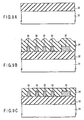
- the polishing cloth of the embodiment is constructed as shown in FIG. 1 or FIG. 2.
- the polishing cloth 1 shown in FIG. 1 is constructed such that a molded body 2 obtained by molding the (meth)acrylic copolymer is fixed to a rotatable turntable 3.
- the polishing cloth 1 shown in FIG. 2 is constructed such that the molded body 2 obtained by molding the (meth)acrylic copolymer is fixed to the rotatable turntable 3 with a buffer material layer 4 such as a rubber layer interposed therebetween.
- the polishing cloth shown in FIG. 2 which has a two-layer structure including the buffer material layer, because the polishing cloth noted above is excellent in its capability of following the undulation of the wafer so as to make it possible to achieve uniform polishing.
- the buffer material layer used in the embodiment is not particularly limited. However, it is desirable to use, for example, a polishing pad of the unwoven fabric type such as Suba-400 or Suba-800 manufactured by Rhodale Inc., rubber or an elastic foam as the buffer material layer 4.
- the polishing cloth formed of the (meth)acrylic copolymer can be manufactured by, for example, a molding method such as a press molding method or an injection molding method. Particularly, since the (meth)acrylic copolymer is satisfactory in its moldability, the polishing cloth can be manufactured by the molding method such as a press molding method or an injection molding method.
- the trench or the hole formed on the surface of the polishing cloth makes it possible to supply a fresh polishing slurry to the polishing region, to improve the fluidity of the polishing slurry, and to discharge the waste polishing slurry or the scrapings.
- the method of forming the trench or the hole is not particularly limited.
- the trench or the hole by the cutting method using an NC rooter, by the method of collectively forming the trench by using a thermal press, by the press molding method or the injection molding method, in which a trench is formed simultaneously with the manufacture of the molded body of the (meth)acrylic copolymer, or by the method of forming a hole by using, for example, a drill.
- the polishing cloth 1 is constructed such that the molded body 2 prepared by, for example, the injection molding of the (meth)acrylic copolymer is fixed to the rotatable turntable 3 with the buffer material layer 4 such as a rubber layer interposed therebetween.
- a supply pipe 5 for supplying a polishing slurry containing abrasive grains, water and, as required, a surfactant and a dispersant onto the molded body 2 is arranged above the polishing cloth 1.
- a holder 7 equipped with a support shaft 6 on the upper surface is arranged to be rotatable above the polishing cloth 1. The holder 7 is also movable in the vertical direction.
- At least one material selected from the group consisting of, for example, cerium oxide, manganese oxide, silica, alumina and zirconia as the abrasive grains contained in the polishing slurry.
- the surfactant contained in the polishing cloth 1 includes, for example, nonionic surfactants such as polyethylene glycol alkyl phenyl ether, polyethylene glycol alkyl ether, polyethylene glycol fatty acid ester; amphoteric surfactants such as imidazolynium betaine; anionic surfactants such as sodium dodecyl sulfate; and cationic surfactants such as stearyl trimethyl ammonium chloride.
- nonionic surfactants such as polyethylene glycol alkyl phenyl ether, polyethylene glycol alkyl ether, polyethylene glycol fatty acid ester
- amphoteric surfactants such as imidazolynium betaine
- anionic surfactants such as sodium dodecyl sulfate
- cationic surfactants such as stearyl trimethyl ammonium chloride.
- polishing treatment using the polishing apparatus having the polishing cloth of the embodiment incorporated therein is carried out as follows.
- a target object 8 to be polished (e.g., a substrate) is held by the holder 7 such that the polishing surface of the target object 8 is allowed to face the molded body 2 of the (meth)acrylic copolymer included in the polishing cloth 1.
- a desired load is applied from the support shaft 6 toward the polishing cloth 1 via the target object 8 to be polished while supplying a polishing slurry 8 containing abrasive grains and water onto the surface of the molded body 2 of the (meth)acrylic copolymer and while rotating the holder 7 and the turntable 3 of the polishing cloth 1 in the same direction.
- the polishing surface of the target object 8 is polished mainly by the abrasive grains contained in the polishing slurry that is supplied into the clearance between the target object 8 and the polishing cloth 1.
- the polishing cloth 1 according to the first embodiment of the present invention comprises the molded body of the (meth)acrylic copolymer having an acid value of 10 to 100 mg KOH/g an a hydroxyl group value of 50 to 150 mg KOH/g.
- the molded body noted above is scarcely dissolved in water and is slightly dissolved in the aqueous solution of potassium hydroxide so as to form a swollen layer on the surface that is in contact with water.
- the polishing slurry containing the abrasive grains and water is supplied onto the polishing cloth (i.e., the polishing cloth having fine irregularities formed thereon by the application of the initial dressing treatment) while allowing the target object 8 to be pushed against the polishing cloth 1 and while rotating the polishing cloth 1 and the target object 8 in the same direction, the abrasive grains contained in the polishing slurry are held in the concavities formed on the surface of the polishing cloth 1.
- the polishing surface of the target object 8 is polished mainly by the abrasive grains held in the concavities on the surface of the polishing cloth 1. Also, a swollen layer is formed on the surface of the polishing cloth 1.
- the polishing cloth 1 receives a frictional force produced by the target object 8 and the abrasive grains, with the result that the swollen layer on the surface of the polishing cloth 1 is scraped off.
- the waste abrasive grains held on the surface of the polishing cloth 1 and the scrapings are also removed from the polishing cloth 1.
- the waste abrasive grains and the scrapings do not stay on the polishing cloth 1 so as to make it possible to supply fresh abrasive grains from the polishing slurry onto the polishing cloth 1.
- the abrasive grains to polish the target object to be polished with high polishing efficiency.
- the target object can be polished while substantially omitting the dressing treatment.
- the polishing cloth formed of the molded body of the (meth)acrylic copolymer containing (meth)acrylic acid units, (meth)acrylic acid hydroxy alkyl ester units, and (meth)acrylic acid alkyl ester units as the constituting units as shown in general formula (I) given previously it is possible to permit the polishing cloth to polish the target object to be polished with high polishing efficiency. It is also possible to stabilize the polishing rate excellently.
- the polishing cloth formed of the molded body of the (meth)acrylic copolymer containing (meth)acrylic acid units, 2-hydroxyethyl (meth)acrylate units, and (meth)acrylic acid alkyl ester units as the constituting units as shown in general formula (II) given previously, it is possible to permit the polishing cloth to polish the target object to be polished with high polishing efficiency. It is also possible to stabilize the polishing rate more excellently.
- the molded body having, for example, a lattice-shaped trench formed thereon, it is possible to release easily the undesired abrasive grains and the polishing refuse from the polishing cloth in the polishing stage.
- the buffering function is produced by the buffer material layer 4 in the polishing stage so as to make it possible to polish soft the target object to be polished.
- a method of a second embodiment for manufacturing a semiconductor device having a shallow trench type element isolating (STI) region will now be described.
- a buffer oxide film is formed first on the surface of a semiconductor substrate, followed by forming a mask material having a hole formed in the shape of the element isolating region. Then, the buffer oxide film and the semiconductor substrate positioned below the buffer oxide film are selectively removed by anisotropic etching such as reactive ion etching so as to form a trench on the semiconductor substrate. After formation of the trench, an insulating film is formed on the entire surface of the mask material including the trench in a thickness larger than the depth of the trench.
- an insulating film such as a silicon nitride film (SiN film) is formed on the buffer oxide film, followed by forming a resist pattern on the silicon nitride film. Then, the silicon nitride film is selectively etched with the resist pattern used as a mask so as to obtain the mask material.
- SiN film silicon nitride film
- a polishing slurry containing the abrasive grains is supplied onto the polishing cloth while allowing the insulating film formed on the semiconductor substrate to abut against the polishing cloth according to the first embodiment described previously and while rotating the polishing cloth and the semiconductor substrate in the same direction so as to apply a chemical mechanical polishing (CMP) treatment to the insulating film until the mask material is exposed to the outside, thereby burying the insulating film in the trench and in the hole formed through the buffer oxide film and the mask material. Then, the mask material and the buffer oxide film are removed so as to form a shallow trench type element isolating (STI) region in which the insulating material is buried in the trench.
- CMP chemical mechanical polishing
- the surface of the formed STI region protrudes from the surface of the semiconductor substrate, it is possible to apply an etching treatment to the insulating material so as to remove the buffer oxide film and to remove slightly that region of the insulating film which is positioned in the hole formed in the mask material before removal of the mask material and the buffer oxide film.
- cerium oxide or silica for forming the abrasive grains.
- the insulating film can be polished in a simplified operating procedure by using the polishing cloth exhibiting a stable polishing performance and without employing the dressing treatment so as to make it possible to manufacture a semiconductor device having an STI region formed therein on a mass production basis.
- a method of a third embodiment for manufacturing a semiconductor device including a flattened interlayer insulating film will now be described.
- An irregular pattern e.g., a gate electrode arranged on a gate insulating film, is formed on a semiconductor substrate having active elements such as diffusion layers formed therein. Then, an interlayer insulating film (first interlayer insulating film) is formed on the irregular pattern. In this stage, the irregular shape caused by the gate electrode is transferred onto the first interlayer insulating film so as to cause the first interlayer insulating film to have a surface having an irregular shape.
- polycrystalline silicon polysilicon
- a metal having a high melting point such as W, Mo or Ti
- a silicide of the metal having a high melting point as the gate electrode material.
- the first interlayer insulating film prefferably be formed of a silicon oxide film prepared by using a silane-based gas or a TEOS-based gas, or to be formed of an inorganic insulating film such as a boron-added glass (BPSG) film or a phosphorus-added glass (PSG) film.
- BPSG boron-added glass
- PSG phosphorus-added glass
- a polishing slurry containing the abrasive grains is supplied onto the polishing cloth while allowing the polishing cloth according to the first embodiment described previously to abut against the first interlayer insulating film formed on the semiconductor substrate and while rotating the polishing cloth and the semiconductor substrate in the same direction so as to apply a chemical mechanical polishing (CMP) treatment to the surface region of the first interlayer insulating film, thereby flattening the surface of the first interlayer insulating film.
- CMP chemical mechanical polishing
- the abrasive grains prefferably be formed of, for example, cerium oxide or silica as in the second embodiment described above.
- the first interlayer insulating film is polished by using the polishing cloth exhibiting a stable polishing performance in a simplified polishing procedure without employing the dressing treatment so as to flatten the surface of the interlayer insulating film. It follows that it is possible to manufacture on a mass production basis the semiconductor device that permits a high precision treatment and also permits fine processing in the subsequent pattern forming process.
- the irregular pattern handled in the third embodiment is not limited to that caused by the gate electrode formed on the semiconductor substrate with the gate insulating film interposed therebetween.
- the irregular pattern caused by the wiring layer is transferred onto the surface of the second interlayer insulating film. It follows that the CMP treatment can be applied to the second interlayer insulating film so as to flatten the surface of the second interlayer insulating film.
- An insulating film is formed on a semiconductor substrate. At least one burying member selected from the group consisting of a concave portion and an aperture portion is formed in the insulating film, followed by forming a conductive material film made of copper or a copper alloy on the entire surface including the burying member.
- the insulating film prefferably be formed of a silicon oxide film prepared by using a silane-based gas or a TEOS-based gas, to be formed of an inorganic insulating film such as a boron-added glass (BPSG) film or a phosphorus-added glass (PSG) film, to be formed of a fluorine-containing insulating film having a low dielectric constant, or to be formed of a low-k film such as an organic film or a porous film. It is acceptable for the insulating film to be covered with a polish stopper film made of, for example, silicon nitride, carbon, alumina, boron nitride or diamond prior to the formation of the conductive material film.
- a polish stopper film made of, for example, silicon nitride, carbon, alumina, boron nitride or diamond prior to the formation of the conductive material film.
- the copper-based metal used as the conductive material includes, for example, copper (Cu) and copper alloys (Cu alloys) such as Cu-Si alloy, Cu-Al alloy, Cu-Si-Al alloy and Cu-Ag alloy.
- the conductive material film noted above can be formed by, for example, a sputter vapor deposition method, a vacuum vapor deposition method or a plating method.
- a conductive material film made of the copper-based metal is formed on the insulating film including the burying member formed on the semiconductor substrate, it is acceptable to form a conductive barrier layer before formation of the conductive material film.
- the conductive barrier layer it is possible to form at least one buried conductive member selected from the group consisting of a wiring layer and a via fill in the burying member surrounded by the conductive barrier layer by applying a polishing treatment to the conductive material film, which is described herein later, after formation of the conductive material film.
- the copper-based metal constituting the conductive member is prevented from being diffused into the insulating film by the conductive barrier layer so as to make it possible to prevent the semiconductor substrate from being contaminated with copper.
- the conductive barrier layer is of a single layer structure or a double layer structure formed of a conductive material selected from the group consisting of a TiN alloy, Ti, Nb, W, a WN alloy, a TaN alloy, a TaSiN alloy, Ta, Co, Zr, a ZrN alloy and a CuTa alloy. It is desirable for the conductive barrier layer to have a thickness falling between 15 and 50 nm.
- a polishing slurry containing the abrasive grains is supplied onto the surface of the polishing cloth while allowing the polishing cloth according to the first embodiment described previously to abut against the conductive material film formed on the semiconductor substrate and while rotating the polishing cloth and the semiconductor substrate in the same direction so as to apply a chemical mechanical polishing (CMP) treatment to the conductive material film until the surface of the insulating film is exposed to the outside.
- CMP chemical mechanical polishing
- the abrasive grains contained in the polishing slurry are formed of silica particles or alumina particles.
- silica particles or alumina particles are used as the abrasive grains.
- the polishing slurry may further contain iron nitrate.
- the polishing slurry may contain a water-soluble organic acid (first organic acid), which reacts with copper contained in the polishing slurry so as to form a copper complex that is substantially insoluble in water and mechanically more brittle than copper, and an oxidizing agent.
- first organic acid water-soluble organic acid
- the first organic acid noted above includes, for example, 2-quinoline carboxylic acid (quinaldic acid), 2-pyridine carboxylic acid, and 2,6-pyridine dicarboxylic acid.
- the first organic acid is contained in the polishing slurry in an amount of at least 0.1% by weight. If the amount of the first organic acid contained in the polishing slurry is smaller than 0.1% by weight, it is difficult to form sufficiently a copper complex that is mechanically more brittle than copper on the surface of copper or a copper alloy. As a result, it is difficult to increase sufficiently the polishing rate of copper or the copper alloy in the polishing stage. It is more desirable for the first organic acid to be contained in, for example, the polishing slurry in an amount falling within a range of between 0.3 and 1.2% by weight.
- the oxidizing agent noted above serves to form a hydrate of copper when the polishing slurry or the polishing composition is brought into contact with copper or a copper alloy. It is possible to use, for example, hydrogen peroxide (H 2 O 2 ) or sodium hypochlorite (NaClO) as the oxidizing agent.
- H 2 O 2 hydrogen peroxide
- NaClO sodium hypochlorite
- the oxidizing agent prefferably be contained in the polishing slurry in an amount that is at least 10 times as much as the weight of the first organic acid. If the amount of the oxidizing agent is smaller than the amount that is 10 times as much as the weight of the first organic acid, it is difficult to promote sufficiently the formation of the copper complex on the surface of copper or the copper alloy. It is more desirable for the amount of the oxidizing agent to be at least 30 times, furthermore desirably, at least 50 times, as much as the weight of the first organic acid.
- polishing slurry for the copper-based metal prefferably contains another organic acid (second organic acid) having at least one carboxyl group and at least one hydroxyl group.
- the second organic acid serves to promote the formation of a copper hydrate performed by the oxidizing agent.
- the second organic acid used in the present invention includes, for example, lactic acid, tartaric acid, mandelic acid, and malic acid. It is possible to use these second organic acids singly or in the form of a mixture of a plurality of these second organic acids. Particularly, it is desirable to use lactic acid as the second organic acid.
- the second organic acid is contained in the polishing slurry in an amount of 20 to 250% by weight based on the amount of the first organic acid. If the amount of the second organic acid is smaller than 20% by weight, it is difficult for the oxidizing agent to produce sufficiently the function of promoting the formation of a copper hydrate. On the other hand, if the amount of the second organic agent exceeds 250% by weight, the conductive material film consisting of copper or a copper alloy tends to etched, resulting in failure to form a pattern. It is more desirable for the second organic acid to be contained in the polishing slurry in an amount of 40 to 200% by weight based on the amount of the first organic acid.
- the conductive material film can be polished in a simplified operation by using a polishing apparatus equipped with the polishing cloth exhibiting a stable polishing performance so as to make it possible to manufacture on a mass production basis a semiconductor device in which a conductive member such as a wiring layer having a desired thickness is formed in the burying member.
- the composition show in Table 1 given below excluding the solvent was charged in a five-mouth flask equipped with a thermometer, a reflux cooler, a dripping pipe, a nitrogen gas introducing pipe and a stirrer, and the composition in the flask was heated to 80°C while stirring the composition and introducing a nitrogen gas into the flask. Then, a mixed liquid system consisting of the monomers for the copolymerization and the polymerization catalyst among the composition shown in Table 1 was dripped into the flask over 3 hours. After completion of the dripping, the reaction system was maintained at the temperature noted above for 6 hours so as to finish the polymerization reaction.
- a mixed liquid material consisting of 92.0 parts by weight of methacrylic acid, 92.8 parts by weight of 2-hydroxyethyl methacrylate, 12.0 parts by weight of methyl methacrylate, 203.2 parts by weight of n-butyl methacrylate, and 3.6 parts by weight of 2,2'-azo bis isobutyronitrile used as a polymerization initiating agent was dripped into the flask over 3 hours. After completion of the dripping, the temperature of the reaction system was maintained at the temperature noted above for 6 hours so as to finish the polymerization reaction.
- reaction system After completion of the dripping, the reaction system was maintained at the temperature noted above for 30 minutes. Then, a mixture consisting of 10.0 parts by weight of xylene and 1.0 parts by weight of Perbutyl I noted above was further dripped into the flask, and the resultant reaction system was kept stirred for 2 hours at the temperature noted above so as to finish the polymerization reaction.
- reaction mixture was diluted by adding 48.0 parts by weight of xylene to the reaction mixture so as to obtain a methacrylic copolymer solution containing 50% by weight of a solid component including the methacrylic copolymer (R-2) having the weight average molecular weight given in Table 2 and not having an acid value and a hydroxyl group value.
- a mixed solution consisting of 13.8 parts by weight of methacrylic acid, 69.6 parts by weight of 2-hydroxyethyl methacrylate, 75.6 parts by weight of methyl methacrylate, 141.0 parts by weight of n-butyl methacrylate, and 8.4 parts by weight of 2,2'-azobis-2,4-dimethyl valeronitrile used as a polymerization initiating agent was charged in the flask, and the resultant reaction system was kept stirred for 30 minutes at room temperature while introducing a nitrogen gas into the reaction system. Further, the reaction system was heated to 60°C and the stirring was continued for 2 hours. Still further, the temperature of the reaction system was elevated to 80°C, and the reaction system was kept stirred for one hour so as to finish the polymerization reaction.
- the resultant suspension was filtered and, then, the filtrate was dried so as to obtain a methacrylic copolymer (S-1) having an average particle diameter of 170 ⁇ m.
- the methacrylic copolymer (S-1) thus obtained was found to have an acid value, a hydroxyl group value and a weight average molecular weight as shown in Table 2 given below.
- the methacrylic copolymers obtained in Synthetic Examples 1 to 3 and Comparative Synthetic Example 1 are represented by structural formula (A) given below.
- Table 2 also shows the amounts (l, m, n, p) of the structural units of structural formula (A), i.e., methacrylic acid (MAA), 2-hydroxyethyl methacrylate (HEMA), methyl methacrylate (MMA), and n-butyl methacrylate (BMA).
- composition of the methacrylic copolymer obtained in Comparative Synthetic Example 2 is given in Table 2 for the sake of convenience in terms of the amounts (n, p) of methyl methacrylate (MMA), and n-butyl methacrylate (BMA), which are constituting units of structural formula (A).
- One surface of an aluminum plate excluding one edge side was coated with a methacrylic copolymer solution containing any of methacrylic copolymers A-1, A-2 and R-1 obtained in Synthetic Examples 1, 2 and Comparative Synthetic Example 1, respectively, followed by drying the coated solution so as to obtain the methacrylic copolymer film having a thickness of 100 ⁇ m. Then, the methacrylic copolymer film was dipped in an ion exchange water of 40°C housed in a container by holding that portion of the Al plate on which the methacrylic copolymer film was not formed. Also, the ion exchange water was stirred by a stirring vane that was rotated at a rotating speed of 200 rpm.
- the Al plate having the methacrylic copolymer film formed thereon was kept dipped in the ion exchange water for 240 minutes so as to measure the change in weight of the methacrylic copolymer film 0 minute later, 60 minutes later, 120 minutes later, 180 minutes later, and 240 minutes later.
- measured were the weight of the Al plate immediately after the coating and drying of the methacrylic copolymer film and the weight (dry weight) of the Al plate the prescribed time after the dipping of the Al plate in the ion exchange water so as to obtain the change in weight of the methacrylic copolymer film on the basis of the difference in the measured value of the weight of the Al plate.
- FIG. 4 is a graph showing the experimental data.
- the negative value of the change in weight denotes that the methacrylic copolymer film eluted into the ion exchange water.
- the three kinds of methacrylic copolymer films as in Comparative Example 1 were formed on one-side surfaces excluding one-side edges of Al plates.
- KOH aqueous solution was stirred by a stirring vane that was rotated at a rotating speed of 200 rpm.
- the aqueous solution of potassium hydroxide was used as a solution of the polishing slurry.
- the Al plate having the methacrylic copolymer film formed thereon was kept dipped in the KOH aqueous solution for 240 minutes so as to measure the change in weight of the methacrylic copolymer film 0 minutes later, 60 minutes later, 120 minutes later, 180 minutes later, and 240 minutes later.
- measured were the weight of the Al plate immediately after the coating and drying of the methacrylic copolymer film and the weight (dry weight) of the Al plate the prescribed time after the dipping of the Al plate in the KOH aqueous solution so as to obtain the change in weight of the methacrylic copolymer film on the basis of the difference in the measured value of the weight of the Al plate.
- FIG. 5 is a graph showing the experimental data.
- the negative value of the change in weight denotes that the methacrylic copolymer film eluted into the ion exchange water.
- the methacrylic copolymer A-1 obtained in Synthetic Example 1 which exhibited an acid value of 30 mg KOH/g, was found to be scarcely dissolved in the KOH aqueous solution even if the methacrylic copolymer film was kept dipped in the KOH aqueous solution for 240 minutes.
- the methacrylic copolymer A-2 obtained in Synthetic Example 2 which exhibited an acid value of 70 mg KOH/g, was found to be slightly dissolved in the KOH aqueous solution.
- the methacrylic copolymer R-1 obtained in Comparative Synthetic Example 1 which exhibited an acid value exceeding 100 mg KOH/g, was found to be dissolved in the KOH aqueous solution in a considerably large amount before the dipping time of the methacrylic copolymer film in the KOH aqueous solution reached 60 minutes.
- the methacrylic copolymer of the present invention which has an acid value falling between 10 and 100 mg KOH/g, is scarcely dissolved in the water (ion exchange water) contained in the polishing slurry and is slightly dissolved in the aqueous solution of potassium hydroxide used in the polishing slurry in which a fine powder, e.g., a silica fine powder, is dispersed.
- a fine powder e.g., a silica fine powder
- a polishing slurry was prepared by dispersing in pure water 1% by weight of cerium oxide abrasive grains having an average grain diameter of 0.2 ⁇ m
- the polishing surface of Suba-400 (trade name of a soft polishing pad of an unwoven fabric type, which is manufactured by Rhodale Inc.) was coated with each of the methacrylic copolymer solutions A-1, A-2 obtained in Synthetic Examples 1, 2 and the methacrylic copolymer solution R-1 obtained in Comparative Synthetic Example 1, followed by drying the coated solution so as to form a polishing layer having a thickness of about 500 ⁇ m, thereby obtaining a polishing cloth of a two-layer type in which the polishing layer was formed on a buffer material layer.
- Suba-400 trade name of a soft polishing pad of an unwoven fabric type, which is manufactured by Rhodale Inc.
- the polishing cloth thus obtained was incorporated in a polishing apparatus MA200 (trade name, manufactured by Musashi Kogyo K.K.), and the molded body of the polishing cloth was subjected to a dressing treatment by using a dressing apparatus equipped with a dressing tool.
- a polishing apparatus MA200 (trade name, manufactured by Musashi Kogyo K.K.)
- prepared was a silicon wafer sized at 20 mm square and having a silicon oxide film formed thereon, followed by allowing the holder of the polishing apparatus to hold the silicon wafer such that the silicon oxide film formed on the silicon wafer was positioned to face the polishing cloth. Under the particular state, the silicon wafer was pushed by the support shaft of the holder against the polishing cloth with a load of about 400 g/cm 2 .
- the polishing slurry was supplied from the supply pipe onto the surface of the polishing cloth at a rate of 10 mL/min while rotating the turntable supporting the polishing cloth and the holder supporting the silicon wafer in the same direction at the rotating speeds of 150 rpm and 112 rpm, respectively, so as to polish the silicon oxide film formed on the surface of the silicon wafer.
- a silicon oxide film formed on the surface of a silicon wafer was polished under the same conditions, except that the polishing cloth incorporated in the polishing apparatus was formed of IC1000 (trade name of a hard polyurethane foam manufactured by Rhodale Inc.) and that the particular polishing cloth was subjected to a dressing treatment by using a dressing apparatus (Prior Art 1).
- IC1000 trade name of a hard polyurethane foam manufactured by Rhodale Inc.
- FIG. 6 is a graph showing the experimental data.
- each of the polishing cloths of the present invention comprising the molded bodies of methacrylic copolymers each having an acid value of 10 to 100 mg KOH/g (i.e., methacrylic copolymers A-1 and A-2 prepared in Synthetic Examples 1 and 2, respectively) exhibits a polishing rate higher than that of the polishing cloth for the Reference Example comprising a methacrylic copolymer having an acid value exceeding 100 mg KOH/g (i.e., methacrylic copolymer R-1 prepared in Comparative Synthetic Example 1).
- the polishing cloth of the present invention comprising the molded boy of methacrylic copolymer having an acid value of 70 mg KOH/g (i.e., methacrylic copolymer A-2 prepared in Synthetic Example 2) exhibits a polishing rate substantially equal to that of the polishing cloth for Prior Art 1, which was formed of IC-1000.
- the polishing cloth of the present invention comprising the molded body of methacrylic copolymer having an acid value of 30 mg KOH/g (i.e., methacrylic copolymer A-1 prepared in Synthetic Example 1) exhibits a polishing rate markedly higher that of the polishing cloth for Prior Art 1, which was formed of IC-1000.
- FIG. 7 is a graph showing the experimental data.
- the polishing cloth for Reference Example comprising the molded body of methacrylic copolymer having an acid value exceeding 100 mg KOH/g (i.e., methacrylic copolymer R-1 prepared in Comparative Synthetic Example 1) was found to be low in its initial polishing rate.
- the polishing rate was lowered with time.
- the polishing rate was lowered by about 60% based on the initial polishing rate in 60 minutes after initiation of the polishing treatment.
- the experimental data support that the polishing rate is changed in the case of using the polishing cloth for Reference Example.
- the experimental data also support that the polishing rate is increased with increase in the polishing time when it comes to the polishing cloth for Prior Art 1, which was formed of a hard polyurethane foam (IC-1000). To be more specific, the polishing rate was increased by about 30% based on the initial polishing rate in 60 minutes after initiation of the polishing treatment. In other words, the experimental data support that the polishing rate is changed in the case of using the polishing cloth for Prior Art 1.
- the polishing rate remains unchanged in 60 minutes after initiation of the polishing treatment in the case of using the polishing cloth of the present invention comprising the molded body of methacrylic copolymer having an acid value of 70 mg KOH/g (i.e., methacrylic copolymer A-2 prepared in Synthetic Example 2), supporting that the particular polishing cloth of the present invention exhibits a highly stable polishing rate.
- the polishing cloth of the present invention comprising the molded body of methacrylic copolymer having an acid value of 30 mg KOH/g (i.e., methacrylic copolymer A-1 prepared in Synthetic Example 1) exhibits a polishing rate markedly higher that of the polishing cloth for Prior Art 1, which was formed of IC-1000.
- the polishing rate is slightly increased with increase in the polishing time, the polishing rate is increased in 60 minutes after initiation of the polishing treatment by only about 16% based on the initial polishing rate, supporting that the particular polishing cloth of the present invention exhibits a stable polishing rate.
- a two-layer type polishing cloth having a polishing layer formed on a buffer material layer was prepared as Prior Art 2 by coating the polishing surface of Suba-400 with a methacrylic copolymer solution containing the methacrylic copolymer R-2 obtained in Comparative Synthetic Example 2, which did not have an acid value and a hydroxyl group value, followed by drying the coated solution so as to form a polishing layer having a thickness of 500 ⁇ m.
- the polishing cloth thus obtained was incorporated in a polishing apparatus similar to that used in Compatative Example 3, and the resultant polishing apparatus was subjected to a dressing treatment and, then, used for polishing a silicon wafer having a silicon oxide film formed thereon as in Comparative Example 3 so as to measure the polishing time and the polishing rate of the silicon oxide film.
- the polishing cloth for Prior Art 2 comprising the methacrylic copolymer R-2, which did not have an acid value and a hydroxyl group value, was found to exhibit a low initial polishing rate of 40 nm/m, though the polishing cloth exhibited a stable polishing rate.
- a polishing slurry was prepared by dispersing 1% by weight of cerium oxide abrasive grains having an average grain diameter of 0.2 ⁇ m in a pure water.
- the methacrylic copolymer S-1 obtained in Synthetic Example 3 was subjected to an injection molding so as to obtain a disk-like molded body having a diameter of 60 cm and a thickness of 3 mm.
- the disk-like molded body thus obtained was attached to a surface of Suba-400 manufactured by Rhodale Inc. by using a double-sided tape, followed by forming a lattice-shaped trench having a width of 2 mm, a depth of 1 mm and a pitch width of 15 mm on the surface of the disk-like molded body so as to prepare a polishing pad of a two-layer structure.
- the polishing pad thus obtained was incorporated in the polishing apparatus shown in FIG. 3 and the molded body of the polishing cloth was subjected to a dressing treatment by using a dressing apparatus comprising a dressing tool.
- the surface of a silicon wafer 21 sized at 8 inches was oxidized so as to form a buffer oxide film 22 having a thickness of about 10 nm, as shown in FIG. 8A.
- a silicon nitride film 23 was deposited in a thickness of 200 nm on the entire surface by the CVD method.
- a resist pattern (not shown), which was selectively removed to form openings in the regions corresponding to the element isolating regions, was formed on the silicon nitride film 23. Then, the silicon nitride film was selectively etched with the resist pattern used as a mask so as to form a mask material 24, as shown in FIG. 8B. After the resist pattern was peeled off for the removal, those portion of the buffer oxide film 22 which were exposed to the outside and the silicon wafer 21 were selectively removed by an anisotropic etching such as a reactive ion etching so as to form trenches 25. Further, a SiO 2 film 26 was deposited by the CVD method on the entire surface of the mask material 24 including the trenches 25 in a thickness larger than the depth of the trench 25, as shown in FIG. 8C.
- the silicon wafer 21 having the SiO 2 film 26 deposited thereon was held by the holder 7 of the polishing apparatus shown in FIG. 3.
- the polishing cloth 1 comprising the molded body of the methacrylic copolymer S-1 referred to above was incorporated in the polishing apparatus shown in FIG. 3, and the silicon wafer 21 was held in a reversed fashion by the holder 7 of the polishing apparatus such that the SiO 2 film 26 formed on the silicon wafer 21 was allowed to face the polishing cloth 1.
- the silicon wafer 21 was pushed by the support shaft 6 of the polishing apparatus so as to impart a load of 400 gf/cm 2 to the polishing cloth 1.
- the polishing slurry was supplied through the supply pipe 5 onto the surface of the polishing cloth 1 at a rate of 190 mL/min while rotating the turntable 3 of the polishing cloth 1 and the holder 7 in the same direction at the rotating speeds of 100 rpm and 107 rpm, respectively, thereby applying a CMP treatment to the SiO 2 film 26 until the surface of the mask material 24 excluding the trenches 25 was exposed to the outside.
- the SiO 2 film 26 was left unremoved within the trenches 25 and within the holes extending through the buffer oxide film 22 and the mask material 24.
- the mask material 24 and the buffer oxide film 22 were removed so as to form a shallow trench type element isolating (STI) region 27 having the SiO 2 film buried in the trench 25, as shown in FIG. 8D.
- STI shallow trench type element isolating
- a SiO 2 film (first interlayer insulating film) 32 having a thickness of, for example, 1000 nm was formed by a CVD method on a silicon wafer 31 having diffusion layers (not shown) such as a source region and a drain region formed therein.
- an Al-Si alloy film was formed on the first interlayer insulating film 32, followed by forming a resist pattern (not shown) on the Al-Si alloy film, as shown in FIG. 9B. Then, anisotropic etching such as reactive ion etching was applied to the Al-Si alloy film with the resist pattern used as a mask so as to form a wiring layer 33.
- a SiO 2 film (second interlayer insulating film) 34 was deposited by a CVD method on the entire surface of the first interlayer insulating film 32 including the wiring layer 33. In this step, the irregular surface shape caused by the formation of the wiring layer 33 was transferred onto the surface of the second interlayer insulating film 34 so as to have the irregular surface shape formed on the second interlayer insulating film 34.
- the silicon wafer 31 was held by the holder 7 of the polishing apparatus shown in FIG. 3.
- the polishing cloth 1 comprising the molded body of the methacrylic copolymer S-1 referred to above was incorporated in the polishing apparatus shown in FIG. 3, and the silicon wafer 31 was held in a reversed fashion by the holder 7 of the polishing apparatus such that the second interlayer insulating film 34 formed on the silicon wafer 31 was allowed to face the polishing cloth 1.
- the silicon wafer 31 was pushed by the support shaft 6 of the polishing apparatus so as to impart a load of 400 gf/cm 2 to the polishing cloth 1.
- the polishing slurry was supplied through the supply pipe 5 onto the surface of the polishing cloth 1 at a rate of 190 mL/min while rotating the turntable 3 of the polishing cloth 1 and the holder 7 in the same direction at the rotating speeds of 100 rpm and 107 rpm, respectively, thereby applying a CMP treatment to the surface of the second interlayer insulating film 34.
- a CMP treatment By this CMP treatment, the surface of the second interlayer insulating film 34 was flattened, as shown in FIG. 9C.
- a polishing slurry containing 3.6% by weight of colloidal silica, 1.1% by weight of colloidal alumina, 0.6% by weight of 2-quinoline carboxylic acid (quinaldic acid), 0.35% by weight of lactic acid, 1.8% by weight of dodecyl aluminum sulfate, 3.9% by weight of hydrogen peroxide, 0.5% by weight of hydroxyethyl cellulose, and the balance of water.
- a barrier layer 44 made of TiN and having a thickness of 15 nm and a Cu film 45 having a thickness of 1.6 ⁇ m were successively formed in the order mentioned by a sputtering vapor deposition method on the SiO 2 film 42 including the trenches 43, as shown in FIG. 10B.
- the silicon wafer 41 having the Cu film 45 formed thereon was held by the holder 7 of the polishing apparatus shown in FIG. 3.
- the polishing cloth 1 comprising the molded body of the methacrylic copolymer S-1 referred to above was incorporated in the polishing apparatus shown in FIG. 3, and the silicon wafer 41 was held in a reversed fashion by the holder 7 of the polishing apparatus such that the Cu film 45 formed on the silicon wafer 41 was allowed to face the polishing cloth 1.
- the silicon wafer 41 was pushed by the support shaft 6 of the polishing apparatus so as to impart a load of 400 gf/cm 2 to the polishing cloth 1.
- the polishing slurry was supplied through the supply pipe 5 onto the polishing cloth 1 at a rate of 50 mL/min while rotating the turntable 3 of the polishing cloth 1 and the holder 7 in the same direction at the rotating speeds of 100 rpm and 107 rpm, respectively, thereby applying a CMP treatment to the Cu film 45 and the barrier layer 44 until the surface of the SiO 2 film 42 excluding the trenches 43 was exposed to the outside.
- a CMP treatment formed was a buried Cu wiring layer 46 surrounded by the barrier layer 44 as shown in FIG. 10C, thereby manufacturing a desired semiconductor device.
- the present invention provides a polishing cloth capable of achieving a stable polishing performance over a long period of time without applying a dressing treatment to the polishing cloth.
- the present invention provides a method of manufacturing a semiconductor device, which permits stably forming a shallow trench type element isolating (STI) region in the semiconductor substrate.
- STI shallow trench type element isolating
- the present invention provides a method of manufacturing a semiconductor device, which permits stably forming an interlayer insulating film having a flattened surface on a semiconductor substrate.
- the present invention provides a method of manufacturing a semiconductor device, which permits stably forming a high-precision conductive member such as a buried wiring layer in at least one burying member selected from the group consisting of a trench and an opening formed in the insulating film on the semiconductor substrate.
Landscapes
- Engineering & Computer Science (AREA)
- Mechanical Engineering (AREA)
- Mechanical Treatment Of Semiconductor (AREA)
- Finish Polishing, Edge Sharpening, And Grinding By Specific Grinding Devices (AREA)
- Addition Polymer Or Copolymer, Post-Treatments, Or Chemical Modifications (AREA)
- Manufacture Of Macromolecular Shaped Articles (AREA)
Description
- The present invention relates to a polishing cloth and a method of manufacturing a semiconductor device.
- It is known in the art that a polishing cloth is used in the manufacturing process of a semiconductor device in the cases where a semiconductor substrate, e.g., a semiconductor wafer, is mirror-finished by the chemical mechanical polishing treatment, where an insulating film is etched back for forming a buried insulating film in the semiconductor wafer (i.e., a buried element isolating region), and where a metal film is etched back for forming a buried wiring.
- The polishing cloth known in the art is constructed to comprise a base body consisting of a hard polyurethane foam or a two-layer structure consisting of a hard polyurethane foam and a polyurethane unwoven fabric, and a surface layer of the base body having fine irregularities. The polishing cloth of the particular construction is used for polishing an insulating film deposited on the surface of a semiconductor wafer having, for example, a trench formed therein so as to form a buried insulating film (i.e., an element isolating region). To be more specific, the semiconductor wafer is held by a holder such that an insulating film, which is to be polished and formed on the semiconductor wafer, is allowed to face the polishing cloth. The semiconductor wafer having the insulating film formed thereon is pushed by the holder toward the polishing cloth under a desired load, and the holder and the polishing cloth are rotated in the same direction while supplying a polishing slurry containing abrasive grains from a supply pipe onto the polishing cloth so as to polish the insulating film formed on the semiconductor wafer.
- In the polishing treatment described above, the abrasive grains contained in the polishing slurry and having a diameter of, for example, about 0.2 µm are loaded in the open cells, which generally have a diameter of 40 to 50 µm, of the polishing cloth so as to be dispersed uniformly between the polishing cloth and the insulating film formed on the semiconductor wafer. The abrasive grains are also held in the polishing cloth portion between the adjacent open cells of the polishing cloth. It follows that the insulating film formed on the semiconductor wafer is mechanically polished.
- However, during the polishing treatment for a long time, the abrasive grains are accumulated in the open cells so as to increase the amount of the abrasive grains present in the polishing cloth portion between the adjacent open cells of the polishing cloth.
In other words, the polishing force produced by the abrasive grains is increased. As a result, the polishing performance fluctuates such that the polishing rate is increased with time, compared with the polishing rate in the initial polishing stage. - It was customary in the past for the polishing cloth in which the polishing performance fluctuated as described above to be processed with a dressing apparatus for regeneration of the polishing cloth. The dressing apparatus noted above comprises a dressing tool of a construction wherein a large number of diamond particles are attached to a metallic base body by means of electrodeposition. However, it is necessary to apply the dressing treatment noted above every time the target object to be polished is subjected to a polishing treatment and, thus, the polishing operation is rendered troublesome. Also, it is possible for the surface of the target object to be polished to be scratched in the polishing stage by the diamond particles dropping from the dressing tool during the treatment with the dressing apparatus.
- On the other hand, a polishing pad that makes it possible to obtain satisfactory polishing characteristics without employing a dressing treatment is disclosed in Japanese Patent Disclosure (Kokai) No. 2001-179607. The polishing pad disclosed in this patent document is formed of a resin, in which the amount of change in the center line average roughness, i.e., the Ra value, after the polishing of a single silicon wafer having an oxide film formed thereon is not larger than 0.2 µm based on the surface irregularity profile formed by the dressing treatment before the polishing stage. For example, the polishing pad noted above is formed of a resin prepared by dispersing polyvinyl pyrrolidone in a liquid phenolic resin or polymethyl methacrylate.
- However, the patent document noted above does not refer to the specific materials in conjunction with the control of the Ra value of the polishing pad. In addition, the polishing pad disclosed in this patent document gives rise to the problem that the polishing rate is lowered.
- In contrast, a polishing pad excellent in polishing characteristics such that damage such as scratches is not generated in the oxide film that is to be polished is disclosed in Japanese Patent Disclosure No. 2001-291685. The polishing pad disclosed in this patent document is prepared by dispersing fine elements having a high molecular weight such as rubber in an acrylic resin such as an acrylic copolymer.
- However, open cells are present on the surface or the polishing pad disclosed in the patent document noted above, with the result that abrasive grains are accumulated in the open cells during the polishing treatment for a long time, giving rise to the problem that the polishing performance fluctuates.
- Further, a polishing cloth capable of exhibiting stable polishing performance over a relatively long time without employing a dressing treatment is disclosed in Japanese Patent Disclosure No. 2002-190460. The polishing cloth disclosed in this patent document includes a polishing layer containing a high molecular weight material such as a silyl ester or a vinyl ether adduct of a carboxylic acid.
- Furthermore, WO 02/28598 (Rodel Holdings, Inc) discloses a method for conditioning polishing pads, which includes pressing a conditioning surface of a conditioning pad comprising a first polymer against a polishing surface of the polishing pad comprising a second polymer, and producing relative motion between the pads such that measure characteristics of the polishing surface are changed.
- US-A-5 942 570 (Matsukura et al) relates to a water-based paint composition which contains a water-dispersible acrylic graft copolymer and internally non-crosslinked acrylic fine particles, and especially to a water-based paint composition suited to metallic paint for automobiles.
- An aspect of the present invention is to provide a polishing cloth capable of exhibiting stable polishing performance for a long time and capable of improving the polishing rate without employing a dressing treatment.
- Another aspect of the present invention is to provide a method of manufacturing a semiconductor device which permits stably forming an element isolating region with high accuracy, the element isolating region consisting of an insulating film buried in a trench formed in a semiconductor substrate.
- Another aspect of the present invention is to provide a method of manufacturing a semiconductor device which permits stably forming an interlayer insulating film having a flattened surface on a semiconductor substrate.
- Further, still another aspect of the present invention is to provide a method of manufacturing a semiconductor device which permits stably forming a conductive member such as a buried wiring layer with high accuracy in at least one burying material selected from the group consisting of a trench and an aperture portion of an insulating film formed on a semiconductor substrate.
- According to an aspect of the present invention, there is provided a polishing cloth used for a chemical mechanical polishing treatment, which comprises a molded body of a (meth)acrylic copolymer having an acid value of 10 to 100 mg KOH/g and a hydroxyl group value of 50 to 150 mg KOH/g.
- According to another aspect of the present invention, there is provided a method of manufacturing a semiconductor device, comprising:
- forming a trench on a semiconductor substrate;
- forming an insulating film on the semiconductor substrate having the trench formed thereon; and
- forming a buried element isolating region by supplying a polishing slurry containing abrasive grains onto the surface of a polishing cloth which comprises a molded body of a (meth)acrylic copolymer having an acid value of 10 to 100 mg KOH/g and a hydroxyl group value of 50 to 150 mg KOH/g, while rotating the semiconductor substrate under the state that the insulating film formed on the semiconductor substrate is allowed to abut against the polishing cloth, thereby polishing the upper portion of the insulating film such that the lower portion of the insulating film is left unremoved inside the trench, the unremoved lower portion of the insulating film forming the buried element isolating region.
- According to another aspect of the present invention, there is provided a method of manufacturing a semiconductor device, comprising:
- forming an interlayer insulating film on an irregular pattern on a semiconductor substrate; and
- supplying a polishing slurry containing abrasive grains onto the surface of a polishing cloth which comprises a molded body of a (meth)acrylic copolymer having an acid value of 10 to 100 mg KOH/g and a hydroxyl group value of 50 to 150 mg KOH/g, while allowing the interlayer insulating film formed on the semiconductor substrate to abut against the polishing cloth, thereby polishing the interlayer insulating film.
- Further, according to still another aspect of the present invention, there is provided a method of manufacturing a semiconductor device, comprising:
- forming an insulating film on a semiconductor substrate;
- forming at least one burying member selected from the group consisting of a trench corresponding to the shape of a wiring layer and an aperture portion corresponding to the shape of a via fill in the insulating film;
- forming a conductive material film on the insulating film including the inner surface of the burying member; and
- supplying a polishing slurry containing abrasive grains onto the surface of a polishing cloth which comprises a molded body of a (meth)acrylic copolymer having an acid value of 10 to 100 mg KOH/g and a hydroxyl group value of 50 to 150 mg KOH/g, while rotating the semiconductor substrate under the state that the conductive material film is allowed to abut against the polishing cloth so as to polish the upper portion of the conductive material film such that the lower portion of the conductive material film is left unremoved inside the burying member, thereby forming at least one conductive member selected from the group consisting of a wiring layer and a via fill.
- The invention can be more fully understood from the following detailed description when taken in conjunction with the accompanying drawings, in which:
- FIG. 1 is a cross-sectional view schematically showing the construction of a polishing cloth according to one embodiment of the present invention;
- FIG. 2 is a cross-sectional view schematically showing the construction of a polishing cloth according to another embodiment of the present invention;
- FIG. 3 schematically shows the construction of a polishing apparatus having the polishing cloth of the present invention incorporated therein;
- FIG. 4 is a graph showing the result of the evaluation in respect of the solubility of three kinds of (meth)acrylic copolymers for Example 1 of the present invention in an ion exchange water;
- FIG. 5 is a graph showing the result of the evaluation in respect of the solubility of three kinds of (meth)acrylic copolymers for Example 2 of the present invention in an aqueous solution of potassium hydroxide;
- FIG. 6 is a graph showing the initial polishing rate of each of the polishing cloths for Example 3 of the present invention;
- FIG. 7 is a graph showing the relationship between the polishing time and the polishing rate for each of the polishing cloths for Example 4 of the present invention;
- FIGS. 8A to 8D are cross-sectional views collectively showing the manufacturing process of a semiconductor device for Example 5 of the present invention;
- FIGS. 9A to 9C are cross-sectional views collectively showing the manufacturing process of a semiconductor device for Example 6 of the present invention; and
- FIGS. 10A to 10C are cross-sectional views collectively showing the manufacturing process of a semiconductor device for Example 7 of the present invention.
- Some embodiments of the present invention will now be described in detail.
- A first embodiment is directed to a polishing cloth used for the chemical mechanical polishing treatment. The polishing cloth comprises a molded body of a (meth)acrylic copolymer having an acid value of 10 to 100 mg KOH/g and a hydroxyl group value of 50 to 150 mg KOH/g.
- The acid value and the hydroxyl group value noted above are measured by the method stipulated in JIS K0070.
- Also, the expression (meth)acrylic copolymer given above implies an acrylic and/or methacrylic copolymer.
- In the (meth)acrylic copolymer noted above, the acid value relates to the swelling properties when the (meth)acrylic copolymer is brought into contact with a polishing slurry containing abrasive grains, and the hydroxyl group value relates to the wettability of the polishing slurry relative to water. Where the acid value and the hydroxyl group value of the (meth)acrylic copolymer are set to fall within the ranges given above, the polishing cloth receives a frictional force in the presence of the polishing slurry containing the abrasive grains so as to exhibit an appropriate self-collapsing properties because of the balance between the acid value and the hydroxyl group value. As a result, it is possible to stabilize and improve the polishing rate.
- Particularly, if the acid value is smaller than 10 mg KOH/g, the swelling properties on the surface of the polishing cloth are rendered low in the presence of the polishing slurry, resulting in failure to obtain an appropriate self-collapsing properties. It follows that it is possible for the stability of the polishing rate to be lowered. On the other hand, if the acid value exceeds 100 mg KOH/g, the swelling properties on the surface of the polishing cloth are rendered excessively high in the presence of the polishing slurry. As a result, the hardness on the surface of the polishing cloth is lowered. It follows that the initial polishing rate tends to be lowered. Also, since the self-collapsing properties are excessively high, it is possible for the stability of the polishing rate to be lowered.
- The (meth)acrylic copolymer can be obtained by the copolymerization of a carboxyl group-containing α,β-unsaturated monomer and a hydroxyl group-containing α,β-unsaturated monomer with another α,β-unsaturated monomer. The carboxyl group-containing α,β-unsaturated monomer used for the copolymerization includes, for example, acrylic acid, methacrylic acid, itaconic acid, mesaconic acid, citraconic acid, maleic acid, and fumaric acid. It is desirable to use acrylic acid or methacrylic acid, particularly, methacrylic acid as the carboxyl group-containing α,β-unsaturated monomer. On the other hand, the hydroxyl group-containing α,β-unsaturated monomer used for the copolymerization noted above includes, for example, 2-hydroxyethyl acrylate, hydroxypropyl acrylate, hydroxybutyl acrylate, acrylic acid polyalkylene glycol ester, 2-hydroxyethyl methacrylate, hydroxypropyl methacrylate, hydroxybutyl methacrylate, and methacrylic acid polyalkylene glycol ester. It is desirable to use 2-hydroxyethyl acrylate, hydroxypropyl acrylate, hydroxybutyl acrylate, 2-hydroxyethyl methacrylate, hydroxypropyl methacrylate, and hydroxybutyl methacrylate, particularly, 2-hydroxyethyl methacrylate as the hydroxyl group-containing α,β-unsaturated monomer. It is possible to use each of the carboxyl group-containing α,β-unsaturated monomer and the hydroxyl group-containing α,β-unsaturated monomer singly or in the form of a mixture of a plurality of the compounds exemplified above.
- To be more specific, it is desirable for the (meth)acrylic copolymer to be represented by general formula (I) given below, in which the atomic group generating the acid value is formed of a constituting unit based on the (meth)acrylic acid, and the atomic group generating the hydroxyl group value is formed of a constituting unit based on the (meth)acrylic acid hydroxyalkyl ester:

- Incidentally, the arrangement of the constituting units of the (meth)acrylic copolymer represented by general formula (I) given above, i.e., the arrangement of (meth)acrylic acid, (meth)acrylic acid hydroxyalkyl ester and (meth)acrylic acid alkyl ester, is not limited to that given in general formula (I). It is possible for these constituting units of the (meth)acrylic copolymer to be interchanged with each other.
- It is more desirable for the (meth)acrylic copolymer to be represented by general formula (II) given below:

- Incidentally, the arrangement of the constituting units of the (meth)acrylic copolymer represented by general formula (II), i.e., the arrangement of (meth)acrylic acid, 2-hydroxyethyl (meth)acrylate and (meth)acrylic acid alkyl ester, is not limited to that given in general formula (II). It is possible for these constituting units of the (meth)acrylic copolymer represented by general formula (II) to be interchanged with each other.
- It is desirable for the alkyl groups represented by R5 and R in general formulas (I) and (II) to have 1 to 18 carbon atoms, preferably 1 to 6 carbon atoms. To be more specific, each of the alkyl groups noted above includes, for example, methyl, ethyl, n-propyl, isopropyl, n-butyl, sec-butyl, isobutyl, n-amyl, isoamyl, sec-amyl, n-pentyl, n-hexyl, cyclohexyl, n-octyl, 2-ethyl hexyl, dodecyl, cetyl and stearyl groups, and it is desirable for each of the alkyl groups to be methyl, ethyl, n-propyl, isopropyl, n-butyl, sec-butyl, isobutyl, n-amyl, isoamyl, see-amyl, n-pentyl, n-hexyl or cyclohexyl group. It should also be noted that the α,β-unsaturated monomer having the alkyl group noted above may be used singly or in the form of a mixture of a plurality of the α,β-unsaturated monomers.
- It is desirable for the (meth)acrylic copolymer to have a weight average molecular weight falling between 40,000 and 1,000,000. If the weight average molecular weight of the (meth)acrylic copolymer is lower than 40,000, it is possible for the mechanical strength of the molded body of the (meth)acrylic copolymer to be lowered. On the other hand, if the weight average molecular weight of the (meth)acrylic copolymer exceeds 1,000,000, the fluidity of the (meth)acrylic copolymer is lowered so as to impair the moldability of the (meth)acrylic copolymer.
- The (meth)acrylic copolymer can be obtained by any of various polymerizing methods such as a solution polymerization method, a bulk polymerization method, an emulsion polymerization method and a suspension polymerization method, which are carried out by the ordinary polymerizing manner in the presence of a vinyl polymerization initiating agent. The vinyl polymerization initiating agent noted above includes azo compounds such as 2,2'-azo bis isobutyronitrile, 2,2'-azo bis-2-methyl butyronitrile, 2,2'-azo bis-2,4-dimethyl valeronitrile, and triphenyl methyl azo benzene and peroxides such as benzoyl peroxide, di-t-butyl peroxide, t-butyl peroxy benzoate, t-butyl peroxy isopropyl carbonate, t-butyl peroxy-2-ethyl hexanoate, t-butyl peroxy pivalate, and t-hexyl peroxy-2-ethyl hexanoate.
- The polishing cloth of the embodiment is constructed as shown in FIG. 1 or FIG. 2. To be more specific, the polishing
cloth 1 shown in FIG. 1 is constructed such that a moldedbody 2 obtained by molding the (meth)acrylic copolymer is fixed to arotatable turntable 3. On the other hand, the polishingcloth 1 shown in FIG. 2 is constructed such that the moldedbody 2 obtained by molding the (meth)acrylic copolymer is fixed to therotatable turntable 3 with abuffer material layer 4 such as a rubber layer interposed therebetween. - Particularly, it is desirable to use the polishing cloth shown in FIG. 2, which has a two-layer structure including the buffer material layer, because the polishing cloth noted above is excellent in its capability of following the undulation of the wafer so as to make it possible to achieve uniform polishing. The buffer material layer used in the embodiment is not particularly limited. However, it is desirable to use, for example, a polishing pad of the unwoven fabric type such as Suba-400 or Suba-800 manufactured by Rhodale Inc., rubber or an elastic foam as the
buffer material layer 4. - The polishing cloth formed of the (meth)acrylic copolymer can be manufactured by, for example, a molding method such as a press molding method or an injection molding method. Particularly, since the (meth)acrylic copolymer is satisfactory in its moldability, the polishing cloth can be manufactured by the molding method such as a press molding method or an injection molding method.
- It is possible to form a trench such as a lattice-shaped trench or a hole on the surface of the polishing cloth of the construction described above. The trench or the hole formed on the surface of the polishing cloth makes it possible to supply a fresh polishing slurry to the polishing region, to improve the fluidity of the polishing slurry, and to discharge the waste polishing slurry or the scrapings. The method of forming the trench or the hole is not particularly limited. For example, it is possible to form the trench or the hole by the cutting method using an NC rooter, by the method of collectively forming the trench by using a thermal press, by the press molding method or the injection molding method, in which a trench is formed simultaneously with the manufacture of the molded body of the (meth)acrylic copolymer, or by the method of forming a hole by using, for example, a drill.
- An example of the polishing apparatus having the polishing cloth of the embodiment incorporated therein will now be described with reference to FIG. 3.
- As shown in FIG. 3, the polishing
cloth 1 is constructed such that the moldedbody 2 prepared by, for example, the injection molding of the (meth)acrylic copolymer is fixed to therotatable turntable 3 with thebuffer material layer 4 such as a rubber layer interposed therebetween. A supply pipe 5 for supplying a polishing slurry containing abrasive grains, water and, as required, a surfactant and a dispersant onto the moldedbody 2 is arranged above the polishingcloth 1. A holder 7 equipped with asupport shaft 6 on the upper surface is arranged to be rotatable above the polishingcloth 1. The holder 7 is also movable in the vertical direction. - It is possible to use at least one material selected from the group consisting of, for example, cerium oxide, manganese oxide, silica, alumina and zirconia as the abrasive grains contained in the polishing slurry.
- The surfactant contained in the polishing
cloth 1 includes, for example, nonionic surfactants such as polyethylene glycol alkyl phenyl ether, polyethylene glycol alkyl ether, polyethylene glycol fatty acid ester; amphoteric surfactants such as imidazolynium betaine; anionic surfactants such as sodium dodecyl sulfate; and cationic surfactants such as stearyl trimethyl ammonium chloride. - The polishing treatment using the polishing apparatus having the polishing cloth of the embodiment incorporated therein is carried out as follows.
- In the first step, a
target object 8 to be polished (e.g., a substrate) is held by the holder 7 such that the polishing surface of thetarget object 8 is allowed to face the moldedbody 2 of the (meth)acrylic copolymer included in the polishingcloth 1. Then, a desired load is applied from thesupport shaft 6 toward the polishingcloth 1 via thetarget object 8 to be polished while supplying a polishingslurry 8 containing abrasive grains and water onto the surface of the moldedbody 2 of the (meth)acrylic copolymer and while rotating the holder 7 and theturntable 3 of the polishingcloth 1 in the same direction. In this stage, the polishing surface of thetarget object 8 is polished mainly by the abrasive grains contained in the polishing slurry that is supplied into the clearance between thetarget object 8 and the polishingcloth 1. - The polishing
cloth 1 according to the first embodiment of the present invention comprises the molded body of the (meth)acrylic copolymer having an acid value of 10 to 100 mg KOH/g an a hydroxyl group value of 50 to 150 mg KOH/g. The molded body noted above is scarcely dissolved in water and is slightly dissolved in the aqueous solution of potassium hydroxide so as to form a swollen layer on the surface that is in contact with water. - If the polishing slurry containing the abrasive grains and water is supplied onto the polishing cloth (i.e., the polishing cloth having fine irregularities formed thereon by the application of the initial dressing treatment) while allowing the
target object 8 to be pushed against the polishingcloth 1 and while rotating the polishingcloth 1 and thetarget object 8 in the same direction, the abrasive grains contained in the polishing slurry are held in the concavities formed on the surface of the polishingcloth 1. The polishing surface of thetarget object 8 is polished mainly by the abrasive grains held in the concavities on the surface of the polishingcloth 1. Also, a swollen layer is formed on the surface of the polishingcloth 1. In this stage, the polishingcloth 1 receives a frictional force produced by thetarget object 8 and the abrasive grains, with the result that the swollen layer on the surface of the polishingcloth 1 is scraped off. When the swollen layer of the polishingcloth 1 is scraped off, the waste abrasive grains held on the surface of the polishingcloth 1 and the scrapings are also removed from the polishingcloth 1. As a result, the waste abrasive grains and the scrapings do not stay on the polishingcloth 1 so as to make it possible to supply fresh abrasive grains from the polishing slurry onto the polishingcloth 1. Such being the situation, it is possible for the abrasive grains to polish the target object to be polished with high polishing efficiency. It is also possible to stabilize the polishing rate. It follows that it is possible to polish the target object without applying a dressing treatment to the polishingcloth 1 for a long time, though it is certainly necessary to apply the initial dressing treatment to the polishingcloth 1. In other words, the target object can be polished while substantially omitting the dressing treatment. - Also, in the case of using the polishing cloth formed of the molded body of the (meth)acrylic copolymer containing (meth)acrylic acid units, (meth)acrylic acid hydroxy alkyl ester units, and (meth)acrylic acid alkyl ester units as the constituting units as shown in general formula (I) given previously, it is possible to permit the polishing cloth to polish the target object to be polished with high polishing efficiency. It is also possible to stabilize the polishing rate excellently.
- Further, in the case of using the polishing cloth formed of the molded body of the (meth)acrylic copolymer containing (meth)acrylic acid units, 2-hydroxyethyl (meth)acrylate units, and (meth)acrylic acid alkyl ester units as the constituting units as shown in general formula (II) given previously, it is possible to permit the polishing cloth to polish the target object to be polished with high polishing efficiency. It is also possible to stabilize the polishing rate more excellently.
- Further, in the case of using as the polishing cloth the molded body having, for example, a lattice-shaped trench formed thereon, it is possible to release easily the undesired abrasive grains and the polishing refuse from the polishing cloth in the polishing stage.
- Still further, in the case where the polishing
cloth 1 is constructed such that the moldedbody 2 formed of the (meth)acrylic copolymer is fixed to theturntable 3 with thebuffer material layer 4 interposed therebetween as shown in FIG. 2, the buffering function is produced by thebuffer material layer 4 in the polishing stage so as to make it possible to polish soft the target object to be polished. - A method of a second embodiment for manufacturing a semiconductor device having a shallow trench type element isolating (STI) region will now be described.
- A buffer oxide film is formed first on the surface of a semiconductor substrate, followed by forming a mask material having a hole formed in the shape of the element isolating region. Then, the buffer oxide film and the semiconductor substrate positioned below the buffer oxide film are selectively removed by anisotropic etching such as reactive ion etching so as to form a trench on the semiconductor substrate. After formation of the trench, an insulating film is formed on the entire surface of the mask material including the trench in a thickness larger than the depth of the trench.
- For forming the mask material, an insulating film such as a silicon nitride film (SiN film) is formed on the buffer oxide film, followed by forming a resist pattern on the silicon nitride film. Then, the silicon nitride film is selectively etched with the resist pattern used as a mask so as to obtain the mask material.
- It is possible to use, for example, a SiO2 film or a TEOS film as the insulating film formed on the mask material.
- A polishing slurry containing the abrasive grains is supplied onto the polishing cloth while allowing the insulating film formed on the semiconductor substrate to abut against the polishing cloth according to the first embodiment described previously and while rotating the polishing cloth and the semiconductor substrate in the same direction so as to apply a chemical mechanical polishing (CMP) treatment to the insulating film until the mask material is exposed to the outside, thereby burying the insulating film in the trench and in the hole formed through the buffer oxide film and the mask material. Then, the mask material and the buffer oxide film are removed so as to form a shallow trench type element isolating (STI) region in which the insulating material is buried in the trench. Incidentally, where the surface of the formed STI region protrudes from the surface of the semiconductor substrate, it is possible to apply an etching treatment to the insulating material so as to remove the buffer oxide film and to remove slightly that region of the insulating film which is positioned in the hole formed in the mask material before removal of the mask material and the buffer oxide film.
- It is possible to use, for example, cerium oxide or silica for forming the abrasive grains.
- As described above, according to the second embodiment, the insulating film can be polished in a simplified operating procedure by using the polishing cloth exhibiting a stable polishing performance and without employing the dressing treatment so as to make it possible to manufacture a semiconductor device having an STI region formed therein on a mass production basis.
- A method of a third embodiment for manufacturing a semiconductor device including a flattened interlayer insulating film will now be described.
- An irregular pattern, e.g., a gate electrode arranged on a gate insulating film, is formed on a semiconductor substrate having active elements such as diffusion layers formed therein. Then, an interlayer insulating film (first interlayer insulating film) is formed on the irregular pattern. In this stage, the irregular shape caused by the gate electrode is transferred onto the first interlayer insulating film so as to cause the first interlayer insulating film to have a surface having an irregular shape.
- It is possible to use, for example, polycrystalline silicon (polysilicon), a metal having a high melting point such as W, Mo or Ti, or a silicide of the metal having a high melting point as the gate electrode material.
- On the other hand, it is possible for the first interlayer insulating film to be formed of a silicon oxide film prepared by using a silane-based gas or a TEOS-based gas, or to be formed of an inorganic insulating film such as a boron-added glass (BPSG) film or a phosphorus-added glass (PSG) film.
- A polishing slurry containing the abrasive grains is supplied onto the polishing cloth while allowing the polishing cloth according to the first embodiment described previously to abut against the first interlayer insulating film formed on the semiconductor substrate and while rotating the polishing cloth and the semiconductor substrate in the same direction so as to apply a chemical mechanical polishing (CMP) treatment to the surface region of the first interlayer insulating film, thereby flattening the surface of the first interlayer insulating film.
- It is possible for the abrasive grains to be formed of, for example, cerium oxide or silica as in the second embodiment described above.
- As described above, according to the third embodiment, the first interlayer insulating film is polished by using the polishing cloth exhibiting a stable polishing performance in a simplified polishing procedure without employing the dressing treatment so as to flatten the surface of the interlayer insulating film. It follows that it is possible to manufacture on a mass production basis the semiconductor device that permits a high precision treatment and also permits fine processing in the subsequent pattern forming process.
- Incidentally, the irregular pattern handled in the third embodiment is not limited to that caused by the gate electrode formed on the semiconductor substrate with the gate insulating film interposed therebetween. For example, it is also possible to apply the third embodiment to a wiring layer formed on the first interlayer insulating film positioned on the semiconductor substrate. In this case, if a second interlayer insulating film is formed on the first interlayer insulating film including the wiring layer, the irregular pattern caused by the wiring layer is transferred onto the surface of the second interlayer insulating film. It follows that the CMP treatment can be applied to the second interlayer insulating film so as to flatten the surface of the second interlayer insulating film.
- A method of a fourth embodiment for manufacturing a semiconductor device equipped with a buried wiring layer will now be described.
- An insulating film is formed on a semiconductor substrate. At least one burying member selected from the group consisting of a concave portion and an aperture portion is formed in the insulating film, followed by forming a conductive material film made of copper or a copper alloy on the entire surface including the burying member.
- It is possible for the insulating film to be formed of a silicon oxide film prepared by using a silane-based gas or a TEOS-based gas, to be formed of an inorganic insulating film such as a boron-added glass (BPSG) film or a phosphorus-added glass (PSG) film, to be formed of a fluorine-containing insulating film having a low dielectric constant, or to be formed of a low-k film such as an organic film or a porous film. It is acceptable for the insulating film to be covered with a polish stopper film made of, for example, silicon nitride, carbon, alumina, boron nitride or diamond prior to the formation of the conductive material film.
- It is possible to use, for example, a copper-based metal or tungsten as the conductive material. The copper-based metal used as the conductive material includes, for example, copper (Cu) and copper alloys (Cu alloys) such as Cu-Si alloy, Cu-Al alloy, Cu-Si-Al alloy and Cu-Ag alloy.
- The conductive material film noted above can be formed by, for example, a sputter vapor deposition method, a vacuum vapor deposition method or a plating method.
- Where a conductive material film made of the copper-based metal is formed on the insulating film including the burying member formed on the semiconductor substrate, it is acceptable to form a conductive barrier layer before formation of the conductive material film. In the case of forming the conductive barrier layer on the insulating film including the burying member, it is possible to form at least one buried conductive member selected from the group consisting of a wiring layer and a via fill in the burying member surrounded by the conductive barrier layer by applying a polishing treatment to the conductive material film, which is described herein later, after formation of the conductive material film. As a result, the copper-based metal constituting the conductive member is prevented from being diffused into the insulating film by the conductive barrier layer so as to make it possible to prevent the semiconductor substrate from being contaminated with copper.
- The conductive barrier layer is of a single layer structure or a double layer structure formed of a conductive material selected from the group consisting of a TiN alloy, Ti, Nb, W, a WN alloy, a TaN alloy, a TaSiN alloy, Ta, Co, Zr, a ZrN alloy and a CuTa alloy. It is desirable for the conductive barrier layer to have a thickness falling between 15 and 50 nm.
- A polishing slurry containing the abrasive grains is supplied onto the surface of the polishing cloth while allowing the polishing cloth according to the first embodiment described previously to abut against the conductive material film formed on the semiconductor substrate and while rotating the polishing cloth and the semiconductor substrate in the same direction so as to apply a chemical mechanical polishing (CMP) treatment to the conductive material film until the surface of the insulating film is exposed to the outside. As a result, the conductive material is buried in the burying member so as to form a buried conductive member such as a buried wiring layer made of copper or a copper alloy.
- Where a copper-based metal is used as the conductive material, the abrasive grains contained in the polishing slurry are formed of silica particles or alumina particles. On the other hand, where tungsten is used as the conductive material, silica particles or alumina particles are used as the abrasive grains.
- Where tungsten is used as the conductive material, it is acceptable for the polishing slurry to further contain iron nitrate.
- Where a copper-based metal is used as the conductive material, it is acceptable for the polishing slurry to contain a water-soluble organic acid (first organic acid), which reacts with copper contained in the polishing slurry so as to form a copper complex that is substantially insoluble in water and mechanically more brittle than copper, and an oxidizing agent.
- The first organic acid noted above includes, for example, 2-quinoline carboxylic acid (quinaldic acid), 2-pyridine carboxylic acid, and 2,6-pyridine dicarboxylic acid.
- It is desirable for the first organic acid to be contained in the polishing slurry in an amount of at least 0.1% by weight. If the amount of the first organic acid contained in the polishing slurry is smaller than 0.1% by weight, it is difficult to form sufficiently a copper complex that is mechanically more brittle than copper on the surface of copper or a copper alloy. As a result, it is difficult to increase sufficiently the polishing rate of copper or the copper alloy in the polishing stage. It is more desirable for the first organic acid to be contained in, for example, the polishing slurry in an amount falling within a range of between 0.3 and 1.2% by weight.
- The oxidizing agent noted above serves to form a hydrate of copper when the polishing slurry or the polishing composition is brought into contact with copper or a copper alloy. It is possible to use, for example, hydrogen peroxide (H2O2) or sodium hypochlorite (NaClO) as the oxidizing agent.
- It is desirable for the oxidizing agent to be contained in the polishing slurry in an amount that is at least 10 times as much as the weight of the first organic acid. If the amount of the oxidizing agent is smaller than the amount that is 10 times as much as the weight of the first organic acid, it is difficult to promote sufficiently the formation of the copper complex on the surface of copper or the copper alloy. It is more desirable for the amount of the oxidizing agent to be at least 30 times, furthermore desirably, at least 50 times, as much as the weight of the first organic acid.
- It is acceptable for the polishing slurry for the copper-based metal to contain another organic acid (second organic acid) having at least one carboxyl group and at least one hydroxyl group.
- The second organic acid serves to promote the formation of a copper hydrate performed by the oxidizing agent. The second organic acid used in the present invention includes, for example, lactic acid, tartaric acid, mandelic acid, and malic acid. It is possible to use these second organic acids singly or in the form of a mixture of a plurality of these second organic acids. Particularly, it is desirable to use lactic acid as the second organic acid.
- It is desirable for the second organic acid to be contained in the polishing slurry in an amount of 20 to 250% by weight based on the amount of the first organic acid. If the amount of the second organic acid is smaller than 20% by weight, it is difficult for the oxidizing agent to produce sufficiently the function of promoting the formation of a copper hydrate. On the other hand, if the amount of the second organic agent exceeds 250% by weight, the conductive material film consisting of copper or a copper alloy tends to etched, resulting in failure to form a pattern. It is more desirable for the second organic acid to be contained in the polishing slurry in an amount of 40 to 200% by weight based on the amount of the first organic acid.
- As described above, according to the fourth embodiment, the conductive material film can be polished in a simplified operation by using a polishing apparatus equipped with the polishing cloth exhibiting a stable polishing performance so as to make it possible to manufacture on a mass production basis a semiconductor device in which a conductive member such as a wiring layer having a desired thickness is formed in the burying member.
- The present invention will now be described more in detail with reference to Examples of the present invention.
- The composition show in Table 1 given below excluding the solvent was charged in a five-mouth flask equipped with a thermometer, a reflux cooler, a dripping pipe, a nitrogen gas introducing pipe and a stirrer, and the composition in the flask was heated to 80°C while stirring the composition and introducing a nitrogen gas into the flask. Then, a mixed liquid system consisting of the monomers for the copolymerization and the polymerization catalyst among the composition shown in Table 1 was dripped into the flask over 3 hours. After completion of the dripping, the reaction system was maintained at the temperature noted above for 6 hours so as to finish the polymerization reaction. As a result, obtained were two kinds of methacrylic copolymer solutions each containing 40% by weight of a solid component including the copolymers denoted by abbreviations in Table 1 given below.
Table 1 Synthetic Example 1 Synthetic Example 2 Mixing ratio (parts by weight) Solvent PGM 298.2 298.2 PMAc 298.2 298.2 Monomers for copolymerization MAA 18.4 43.2 HEMA 92.8 92.8 MMA 100.8 70.0 BMA 188.0 194.0 Polymerization initiating agent AIBN 3.6 3.6 Weight average molecular weight 57,000 42,000 Acid value (mgKOH/g) 30 70 Hydroxyl group value (mgKOH/g) 100 100 Abbreviation of methacrylic copolymer (A-1) (A-2) - The abbreviations of the raw materials shown in Table 1 denote the compounds given below:
- PGM: propylene glycol monomethyl ether;
- PMAc: propylene glycol monomethyl ether acetate;
- MAA: methacrylic acid;
- HEMA: 2-hydroxyethyl methacrylate;
- MMA: methyl methacrylate;
- BMA: n-butyl methacrylate;
- AIBN: 2,2'-azo bis isobutyronitrile;
- Charged in a five-mouth flask equipped with a thermometer, a reflux cooler, a dripping pipe, a nitrogen gas introducing pipe, and a stirrer were 298.2 parts by weight of propylene glycol monomethyl ether and 298.2 parts by weight of propylene glycol monomethyl ether acetate. Then, the charged materials were heated to 80°C while stirring the charged materials and introducing a nitrogen gas into the flask. In the next step, a mixed liquid material consisting of 92.0 parts by weight of methacrylic acid, 92.8 parts by weight of 2-hydroxyethyl methacrylate, 12.0 parts by weight of methyl methacrylate, 203.2 parts by weight of n-butyl methacrylate, and 3.6 parts by weight of 2,2'-azo bis isobutyronitrile used as a polymerization initiating agent was dripped into the flask over 3 hours. After completion of the dripping, the temperature of the reaction system was maintained at the temperature noted above for 6 hours so as to finish the polymerization reaction. As a result, obtained was a methacrylic copolymer solution containing 40% by weight of a solid component including the methacrylic copolymer (R-1) having the acid value, the hydroxyl group value and the weight average molecular weight shown in Table 2.
- Charged in a five-mouth flask equipped with a thermometer, a reflux cooler, a nitrogen gas introducing pipe, and a stirrer were 40.0 parts by weight of xylene, and 10.0 parts by weight of butyl acetate. Then, the mixture of the charged materials was heated to 134°C, and a mixed liquid system consisting of 15.0 parts by weight of methyl methacrylate, 85.0 parts by weight of n-butyl methacrylate, and 1.0 parts by weight of a polymerization catalyst "Perbutyl I" (trade name of t-butyl peroxy isopropyl carbonate manufactured by Japan Fat and Oil K.K.) was dripped into the flask over 3 hours. After completion of the dripping, the reaction system was maintained at the temperature noted above for 30 minutes. Then, a mixture consisting of 10.0 parts by weight of xylene and 1.0 parts by weight of Perbutyl I noted above was further dripped into the flask, and the resultant reaction system was kept stirred for 2 hours at the temperature noted above so as to finish the polymerization reaction.
- Finally, the reaction mixture was diluted by adding 48.0 parts by weight of xylene to the reaction mixture so as to obtain a methacrylic copolymer solution containing 50% by weight of a solid component including the methacrylic copolymer (R-2) having the weight average molecular weight given in Table 2 and not having an acid value and a hydroxyl group value.
- Charged in a four-mouth flask equipped with a thermometer, a reflux cooler, a nitrogen gas introducing pipe and a stirrer were 1,200.0 parts by weight of an ion exchange water, and 0.75 parts by weight of polyvinyl alcohol used as a dispersant. Then, the polyvinyl alcohol was dissolved in the ion exchange water by sufficiently stirring the ion exchange water. Further, a mixed solution consisting of 13.8 parts by weight of methacrylic acid, 69.6 parts by weight of 2-hydroxyethyl methacrylate, 75.6 parts by weight of methyl methacrylate, 141.0 parts by weight of n-butyl methacrylate, and 8.4 parts by weight of 2,2'-azobis-2,4-dimethyl valeronitrile used as a polymerization initiating agent was charged in the flask, and the resultant reaction system was kept stirred for 30 minutes at room temperature while introducing a nitrogen gas into the reaction system. Further, the reaction system was heated to 60°C and the stirring was continued for 2 hours. Still further, the temperature of the reaction system was elevated to 80°C, and the reaction system was kept stirred for one hour so as to finish the polymerization reaction.
- The resultant suspension was filtered and, then, the filtrate was dried so as to obtain a methacrylic copolymer (S-1) having an average particle diameter of 170 µm. The methacrylic copolymer (S-1) thus obtained was found to have an acid value, a hydroxyl group value and a weight average molecular weight as shown in Table 2 given below.
- Incidentally, the methacrylic copolymers obtained in Synthetic Examples 1 to 3 and Comparative Synthetic Example 1 are represented by structural formula (A) given below. Table 2 also shows the amounts (l, m, n, p) of the structural units of structural formula (A), i.e., methacrylic acid (MAA), 2-hydroxyethyl methacrylate (HEMA), methyl methacrylate (MMA), and n-butyl methacrylate (BMA). Also, the composition of the methacrylic copolymer obtained in Comparative Synthetic Example 2 is given in Table 2 for the sake of convenience in terms of the amounts (n, p) of methyl methacrylate (MMA), and n-butyl methacrylate (BMA), which are constituting units of structural formula (A).
Table 2 Methacrylic copolymer A-1 (present invention) A-2 (present invention) R-1 (Reference Example) R-2 (prior art 2) S-1 (present invention) MAA:1(wt%) 4.6 10.8 23.0 - 4.4 HEMA:m(wt%) 23.2 23.2 23.2 - 22.5 MMA:n(wt%) 25.2 17.5 3.0 15.0 25.5 BMA:p(wt%) 47.0 48.5 50.8 85.0 47.6 Acid value (mgKOH/g) 30 70 150 - 28.4 Hydroxyl group value (mgKOH/g) 100 100 100 - 96.8 Weight average molecular weight 57,000 42,000 84,000 45,000 361,000 
- One surface of an aluminum plate excluding one edge side was coated with a methacrylic copolymer solution containing any of methacrylic copolymers A-1, A-2 and R-1 obtained in Synthetic Examples 1, 2 and Comparative Synthetic Example 1, respectively, followed by drying the coated solution so as to obtain the methacrylic copolymer film having a thickness of 100 µm. Then, the methacrylic copolymer film was dipped in an ion exchange water of 40°C housed in a container by holding that portion of the Al plate on which the methacrylic copolymer film was not formed. Also, the ion exchange water was stirred by a stirring vane that was rotated at a rotating speed of 200 rpm. The Al plate having the methacrylic copolymer film formed thereon was kept dipped in the ion exchange water for 240 minutes so as to measure the change in weight of the
methacrylic copolymer film 0 minute later, 60 minutes later, 120 minutes later, 180 minutes later, and 240 minutes later. In other words, measured were the weight of the Al plate immediately after the coating and drying of the methacrylic copolymer film and the weight (dry weight) of the Al plate the prescribed time after the dipping of the Al plate in the ion exchange water so as to obtain the change in weight of the methacrylic copolymer film on the basis of the difference in the measured value of the weight of the Al plate. FIG. 4 is a graph showing the experimental data. The negative value of the change in weight denotes that the methacrylic copolymer film eluted into the ion exchange water. - As is apparent from the experimental data given in FIG. 4, any of the methacrylic copolymer films A-1, A-2 obtained in Synthetic Examples 1 and 2 and the methacrylic copolymer film R-1 obtained in Comparative Synthetic Example 1 was found to be scarcely dissolved in the ion exchange water even if these methacrylic copolymer films were dipped in the ion exchange water for 240-minutes.
- The three kinds of methacrylic copolymer films as in Comparative Example 1 were formed on one-side surfaces excluding one-side edges of Al plates. Each of these methacrylic copolymer films was dipped in an aqueous solution of potassium hydroxide (KOH aqueous solution: pH = 11), which was heated to 40°C and housed in a container, by holding that portion of the Al plate on which the methacrylic copolymer film was not formed. Also, the KOH aqueous solution was stirred by a stirring vane that was rotated at a rotating speed of 200 rpm. The aqueous solution of potassium hydroxide was used as a solution of the polishing slurry. The Al plate having the methacrylic copolymer film formed thereon was kept dipped in the KOH aqueous solution for 240 minutes so as to measure the change in weight of the
methacrylic copolymer film 0 minutes later, 60 minutes later, 120 minutes later, 180 minutes later, and 240 minutes later. In other words, measured were the weight of the Al plate immediately after the coating and drying of the methacrylic copolymer film and the weight (dry weight) of the Al plate the prescribed time after the dipping of the Al plate in the KOH aqueous solution so as to obtain the change in weight of the methacrylic copolymer film on the basis of the difference in the measured value of the weight of the Al plate. FIG. 5 is a graph showing the experimental data. The negative value of the change in weight denotes that the methacrylic copolymer film eluted into the ion exchange water. - As is apparent from the experimental data given in FIG. 5, the methacrylic copolymer A-1 obtained in Synthetic Example 1, which exhibited an acid value of 30 mg KOH/g, was found to be scarcely dissolved in the KOH aqueous solution even if the methacrylic copolymer film was kept dipped in the KOH aqueous solution for 240 minutes. Also, the methacrylic copolymer A-2 obtained in Synthetic Example 2, which exhibited an acid value of 70 mg KOH/g, was found to be slightly dissolved in the KOH aqueous solution.
- On the other hand, the methacrylic copolymer R-1 obtained in Comparative Synthetic Example 1, which exhibited an acid value exceeding 100 mg KOH/g, was found to be dissolved in the KOH aqueous solution in a considerably large amount before the dipping time of the methacrylic copolymer film in the KOH aqueous solution reached 60 minutes.
- As is apparent from the experimental data obtained in Comparative Examples 1 and 2, the methacrylic copolymer of the present invention, which has an acid value falling between 10 and 100 mg KOH/g, is scarcely dissolved in the water (ion exchange water) contained in the polishing slurry and is slightly dissolved in the aqueous solution of potassium hydroxide used in the polishing slurry in which a fine powder, e.g., a silica fine powder, is dispersed. In other words, the methacrylic copolymer of the present invention is scraped off only when the methacrylic copolymer substantially receives a frictional force in the presence of the polishing slurry.
- A polishing slurry was prepared by dispersing in
pure water 1% by weight of cerium oxide abrasive grains having an average grain diameter of 0.2 µm - On the other hand, the polishing surface of Suba-400 (trade name of a soft polishing pad of an unwoven fabric type, which is manufactured by Rhodale Inc.) was coated with each of the methacrylic copolymer solutions A-1, A-2 obtained in Synthetic Examples 1, 2 and the methacrylic copolymer solution R-1 obtained in Comparative Synthetic Example 1, followed by drying the coated solution so as to form a polishing layer having a thickness of about 500 µm, thereby obtaining a polishing cloth of a two-layer type in which the polishing layer was formed on a buffer material layer. The polishing cloth thus obtained was incorporated in a polishing apparatus MA200 (trade name, manufactured by Musashi Kogyo K.K.), and the molded body of the polishing cloth was subjected to a dressing treatment by using a dressing apparatus equipped with a dressing tool.
- In the next step, prepared was a silicon wafer sized at 20 mm square and having a silicon oxide film formed thereon, followed by allowing the holder of the polishing apparatus to hold the silicon wafer such that the silicon oxide film formed on the silicon wafer was positioned to face the polishing cloth. Under the particular state, the silicon wafer was pushed by the support shaft of the holder against the polishing cloth with a load of about 400 g/cm2. Also, the polishing slurry was supplied from the supply pipe onto the surface of the polishing cloth at a rate of 10 mL/min while rotating the turntable supporting the polishing cloth and the holder supporting the silicon wafer in the same direction at the rotating speeds of 150 rpm and 112 rpm, respectively, so as to polish the silicon oxide film formed on the surface of the silicon wafer.
- Also, a silicon oxide film formed on the surface of a silicon wafer was polished under the same conditions, except that the polishing cloth incorporated in the polishing apparatus was formed of IC1000 (trade name of a hard polyurethane foam manufactured by Rhodale Inc.) and that the particular polishing cloth was subjected to a dressing treatment by using a dressing apparatus (Prior Art 1).
- The silicon oxide film was polished by using a polishing apparatus having each of the four kinds of the polishing cloths incorporated therein so as to measure the polishing rate in the initial polishing stage of the silicon oxide film. FIG. 6 is a graph showing the experimental data.
- As is apparent from the experimental data given in FIG. 6, each of the polishing cloths of the present invention comprising the molded bodies of methacrylic copolymers each having an acid value of 10 to 100 mg KOH/g (i.e., methacrylic copolymers A-1 and A-2 prepared in Synthetic Examples 1 and 2, respectively) exhibits a polishing rate higher than that of the polishing cloth for the Reference Example comprising a methacrylic copolymer having an acid value exceeding 100 mg KOH/g (i.e., methacrylic copolymer R-1 prepared in Comparative Synthetic Example 1). Particularly, the polishing cloth of the present invention comprising the molded boy of methacrylic copolymer having an acid value of 70 mg KOH/g (i.e., methacrylic copolymer A-2 prepared in Synthetic Example 2) exhibits a polishing rate substantially equal to that of the polishing cloth for
Prior Art 1, which was formed of IC-1000. On the other hand, the polishing cloth of the present invention comprising the molded body of methacrylic copolymer having an acid value of 30 mg KOH/g (i.e., methacrylic copolymer A-1 prepared in Synthetic Example 1) exhibits a polishing rate markedly higher that of the polishing cloth forPrior Art 1, which was formed of IC-1000. - The polishing time and the polishing rate of a silicon oxide film were measured by performing a polishing treatment of the silicon oxide film by using a polishing apparatus having each of the four kinds of the polishing cloths, which were prepared in Comparative Example 3, incorporated therein. FIG. 7 is a graph showing the experimental data.
- As is apparent from the experimental data given in FIG. 7, the polishing cloth for Reference Example comprising the molded body of methacrylic copolymer having an acid value exceeding 100 mg KOH/g (i.e., methacrylic copolymer R-1 prepared in Comparative Synthetic Example 1) was found to be low in its initial polishing rate. In addition, the polishing rate was lowered with time. To be more specific, the polishing rate was lowered by about 60% based on the initial polishing rate in 60 minutes after initiation of the polishing treatment. In other words, the experimental data support that the polishing rate is changed in the case of using the polishing cloth for Reference Example.
- The experimental data also support that the polishing rate is increased with increase in the polishing time when it comes to the polishing cloth for
Prior Art 1, which was formed of a hard polyurethane foam (IC-1000). To be more specific, the polishing rate was increased by about 30% based on the initial polishing rate in 60 minutes after initiation of the polishing treatment. In other words, the experimental data support that the polishing rate is changed in the case of using the polishing cloth forPrior Art 1. - On the other hand, the polishing rate remains unchanged in 60 minutes after initiation of the polishing treatment in the case of using the polishing cloth of the present invention comprising the molded body of methacrylic copolymer having an acid value of 70 mg KOH/g (i.e., methacrylic copolymer A-2 prepared in Synthetic Example 2), supporting that the particular polishing cloth of the present invention exhibits a highly stable polishing rate.
- Also, the polishing cloth of the present invention comprising the molded body of methacrylic copolymer having an acid value of 30 mg KOH/g (i.e., methacrylic copolymer A-1 prepared in Synthetic Example 1) exhibits a polishing rate markedly higher that of the polishing cloth for
Prior Art 1, which was formed of IC-1000. In addition, although the polishing rate is slightly increased with increase in the polishing time, the polishing rate is increased in 60 minutes after initiation of the polishing treatment by only about 16% based on the initial polishing rate, supporting that the particular polishing cloth of the present invention exhibits a stable polishing rate. - Incidentally, a two-layer type polishing cloth having a polishing layer formed on a buffer material layer was prepared as
Prior Art 2 by coating the polishing surface of Suba-400 with a methacrylic copolymer solution containing the methacrylic copolymer R-2 obtained in Comparative Synthetic Example 2, which did not have an acid value and a hydroxyl group value, followed by drying the coated solution so as to form a polishing layer having a thickness of 500 µm. The polishing cloth thus obtained was incorporated in a polishing apparatus similar to that used in Compatative Example 3, and the resultant polishing apparatus was subjected to a dressing treatment and, then, used for polishing a silicon wafer having a silicon oxide film formed thereon as in Comparative Example 3 so as to measure the polishing time and the polishing rate of the silicon oxide film. As a result, the polishing cloth forPrior Art 2 comprising the methacrylic copolymer R-2, which did not have an acid value and a hydroxyl group value, was found to exhibit a low initial polishing rate of 40 nm/m, though the polishing cloth exhibited a stable polishing rate. - A polishing slurry was prepared by dispersing 1% by weight of cerium oxide abrasive grains having an average grain diameter of 0.2 µm in a pure water.
- On the other hand, the methacrylic copolymer S-1 obtained in Synthetic Example 3 was subjected to an injection molding so as to obtain a disk-like molded body having a diameter of 60 cm and a thickness of 3 mm. The disk-like molded body thus obtained was attached to a surface of Suba-400 manufactured by Rhodale Inc. by using a double-sided tape, followed by forming a lattice-shaped trench having a width of 2 mm, a depth of 1 mm and a pitch width of 15 mm on the surface of the disk-like molded body so as to prepare a polishing pad of a two-layer structure. The polishing pad thus obtained was incorporated in the polishing apparatus shown in FIG. 3 and the molded body of the polishing cloth was subjected to a dressing treatment by using a dressing apparatus comprising a dressing tool.
- In the next step, the surface of a
silicon wafer 21 sized at 8 inches was oxidized so as to form a buffer oxide film 22 having a thickness of about 10 nm, as shown in FIG. 8A. Then, a silicon nitride film 23 was deposited in a thickness of 200 nm on the entire surface by the CVD method. - After deposition of the silicon nitride film 23, a resist pattern (not shown), which was selectively removed to form openings in the regions corresponding to the element isolating regions, was formed on the silicon nitride film 23. Then, the silicon nitride film was selectively etched with the resist pattern used as a mask so as to form a
mask material 24, as shown in FIG. 8B. After the resist pattern was peeled off for the removal, those portion of the buffer oxide film 22 which were exposed to the outside and thesilicon wafer 21 were selectively removed by an anisotropic etching such as a reactive ion etching so as to formtrenches 25. Further, a SiO2 film 26 was deposited by the CVD method on the entire surface of themask material 24 including thetrenches 25 in a thickness larger than the depth of thetrench 25, as shown in FIG. 8C. - In the next step, the
silicon wafer 21 having the SiO2 film 26 deposited thereon was held by the holder 7 of the polishing apparatus shown in FIG. 3. Incidentally, the polishingcloth 1 comprising the molded body of the methacrylic copolymer S-1 referred to above was incorporated in the polishing apparatus shown in FIG. 3, and thesilicon wafer 21 was held in a reversed fashion by the holder 7 of the polishing apparatus such that the SiO2 film 26 formed on thesilicon wafer 21 was allowed to face the polishingcloth 1. Thesilicon wafer 21 was pushed by thesupport shaft 6 of the polishing apparatus so as to impart a load of 400 gf/cm2 to the polishingcloth 1. Also, the polishing slurry was supplied through the supply pipe 5 onto the surface of the polishingcloth 1 at a rate of 190 mL/min while rotating theturntable 3 of the polishingcloth 1 and the holder 7 in the same direction at the rotating speeds of 100 rpm and 107 rpm, respectively, thereby applying a CMP treatment to the SiO2 film 26 until the surface of themask material 24 excluding thetrenches 25 was exposed to the outside. By this CMP treatment, the SiO2 film 26 was left unremoved within thetrenches 25 and within the holes extending through the buffer oxide film 22 and themask material 24. Finally, themask material 24 and the buffer oxide film 22 were removed so as to form a shallow trench type element isolating (STI)region 27 having the SiO2 film buried in thetrench 25, as shown in FIG. 8D. - The particular CMP treatment described above was consecutively applied to the
silicon wafer 21, which corresponded to the polishing of 40 silicon wafers, with the result that it was possible to form stably the shallow trench type element isolating (STI)region 27 satisfactorily in any of all thesilicon wafers 21. - As shown in FIG. 9A, a SiO2 film (first interlayer insulating film) 32 having a thickness of, for example, 1000 nm was formed by a CVD method on a
silicon wafer 31 having diffusion layers (not shown) such as a source region and a drain region formed therein. - In the next step, an Al-Si alloy film was formed on the first
interlayer insulating film 32, followed by forming a resist pattern (not shown) on the Al-Si alloy film, as shown in FIG. 9B. Then, anisotropic etching such as reactive ion etching was applied to the Al-Si alloy film with the resist pattern used as a mask so as to form awiring layer 33. After formation of thewiring layer 33, a SiO2 film (second interlayer insulating film) 34 was deposited by a CVD method on the entire surface of the firstinterlayer insulating film 32 including thewiring layer 33. In this step, the irregular surface shape caused by the formation of thewiring layer 33 was transferred onto the surface of the secondinterlayer insulating film 34 so as to have the irregular surface shape formed on the secondinterlayer insulating film 34. - In the next step, the
silicon wafer 31 was held by the holder 7 of the polishing apparatus shown in FIG. 3. Incidentally, the polishingcloth 1 comprising the molded body of the methacrylic copolymer S-1 referred to above was incorporated in the polishing apparatus shown in FIG. 3, and thesilicon wafer 31 was held in a reversed fashion by the holder 7 of the polishing apparatus such that the secondinterlayer insulating film 34 formed on thesilicon wafer 31 was allowed to face the polishingcloth 1. Thesilicon wafer 31 was pushed by thesupport shaft 6 of the polishing apparatus so as to impart a load of 400 gf/cm2 to the polishingcloth 1. Also, the polishing slurry was supplied through the supply pipe 5 onto the surface of the polishingcloth 1 at a rate of 190 mL/min while rotating theturntable 3 of the polishingcloth 1 and the holder 7 in the same direction at the rotating speeds of 100 rpm and 107 rpm, respectively, thereby applying a CMP treatment to the surface of the secondinterlayer insulating film 34. By this CMP treatment, the surface of the secondinterlayer insulating film 34 was flattened, as shown in FIG. 9C. - The particular CMP treatment described above was consecutively applied to the
silicon wafer 31, which corresponded to the polishing of 40 silicon wafers, with the result that it was possible to flatten stably the surface of the secondinterlayer insulating film 34 formed on any of all thesilicon wafers 31. - In the first step, prepared was a polishing slurry containing 3.6% by weight of colloidal silica, 1.1% by weight of colloidal alumina, 0.6% by weight of 2-quinoline carboxylic acid (quinaldic acid), 0.35% by weight of lactic acid, 1.8% by weight of dodecyl aluminum sulfate, 3.9% by weight of hydrogen peroxide, 0.5% by weight of hydroxyethyl cellulose, and the balance of water.
- On the other hand, a SiO2 film 42 having a thickness of, for example, 100 nm, which was used as an interlayer insulating film, was formed by a CVD method on the surface of a
silicon wafer 41 having diffusion layers (not shown) such as a source region and drain region formed therein, as shown in FIG. 10A. Then, a plurality oftrenches 43 each having a shape corresponding to the wiring layer and each having a width of 100 µm and a depth of 0.8 µm were formed by the photo-etching technology in the SiO2 film 42. After formation of thetrenches 43, abarrier layer 44 made of TiN and having a thickness of 15 nm and aCu film 45 having a thickness of 1.6 µm were successively formed in the order mentioned by a sputtering vapor deposition method on the SiO2 film 42 including thetrenches 43, as shown in FIG. 10B. - In the next step, the
silicon wafer 41 having theCu film 45 formed thereon was held by the holder 7 of the polishing apparatus shown in FIG. 3. Incidentally, the polishingcloth 1 comprising the molded body of the methacrylic copolymer S-1 referred to above was incorporated in the polishing apparatus shown in FIG. 3, and thesilicon wafer 41 was held in a reversed fashion by the holder 7 of the polishing apparatus such that theCu film 45 formed on thesilicon wafer 41 was allowed to face the polishingcloth 1. Thesilicon wafer 41 was pushed by thesupport shaft 6 of the polishing apparatus so as to impart a load of 400 gf/cm2 to the polishingcloth 1. Also, the polishing slurry was supplied through the supply pipe 5 onto the polishingcloth 1 at a rate of 50 mL/min while rotating theturntable 3 of the polishingcloth 1 and the holder 7 in the same direction at the rotating speeds of 100 rpm and 107 rpm, respectively, thereby applying a CMP treatment to theCu film 45 and thebarrier layer 44 until the surface of the SiO2 film 42 excluding thetrenches 43 was exposed to the outside. By this CMP treatment, formed was a buriedCu wiring layer 46 surrounded by thebarrier layer 44 as shown in FIG. 10C, thereby manufacturing a desired semiconductor device. - The particular CMP treatment described above was consecutively applied to the
silicon wafer 41, which corresponded to the polishing of 40 silicon wafers, with the result that it was possible to stably form a satisfactory buriedCu wiring layer 46 in any of all thesilicon wafers 41. - As described above in detail, the present invention provides a polishing cloth capable of achieving a stable polishing performance over a long period of time without applying a dressing treatment to the polishing cloth.
- Also, the present invention provides a method of manufacturing a semiconductor device, which permits stably forming a shallow trench type element isolating (STI) region in the semiconductor substrate.
- Further, the present invention provides a method of manufacturing a semiconductor device, which permits stably forming an interlayer insulating film having a flattened surface on a semiconductor substrate.
- Still further, the present invention provides a method of manufacturing a semiconductor device, which permits stably forming a high-precision conductive member such as a buried wiring layer in at least one burying member selected from the group consisting of a trench and an opening formed in the insulating film on the semiconductor substrate.
Claims (33)
- A polishing cloth (1) used for a chemical mechanical polishing treatment, which comprises a molded body (2) of a (meth)acrylic copolymer having an acid value of 10 to 100 mg KOH/g and a hydroxyl group value of 50 to 150 mg KOH/g.
- The polishing cloth according to claim 1, characterized in that the (meth)acrylic copolymer is represented by general formula (I) given below, in which the atomic group generating the acid value is formed of a constituting unit based on the (meth)acrylic acid, and the atomic group generating the hydroxyl group value is formed of a constituting unit based on the (meth)acrylic acid hydroxyalkyl ester:

- The polishing cloth according to claim 1, characterized in that the (meth)acrylic copolymer is represented by general formula (II) given below, in which the atomic group generating the acid value is formed of a constituting unit based on the (meth)acrylic acid, and the atomic group generating the hydroxyl group value is formed of a constituting unit based on 2-hydroxyethyl (meth)acrylate:

- The polishing cloth according to claim 1, characterized in that the (meth)acrylic copolymer has a weight average molecular weight in the range of 40,000 to 1,000,000.
- The polishing cloth (1) according to claim 1, characterized in that the molded body (2) of the (meth)acrylic copolymer is fixed directly to a turntable (3) that can be rotated.
- The polishing cloth (1) according to claim 1, characterized in that the molded body (2) of the (meth)acrylic copolymer is fixed to a turntable (3) that can be rotated with a buffer material layer (4) interposed between the molded body and the turntable.
- The polishing cloth according to claim 6, characterized in that the buffer material layer (4) is selected from the group consisting of an unwoven fabric type polishing pad, a rubber layer and an elastic foamed layer.
- A method of manufacturing a semiconductor device, characterized by comprising:forming a trench (25) on a semiconductor substrate (21);forming an insulating film (26) on the semiconductor substrate (21) having the trench (25) formed thereon; andforming a buried element isolating region (27) by supplying a polishing slurry containing abrasive grains onto the surface of a polishing cloth (1) which comprises a molded body (2) of a (meth)acrylic copolymer having an acid value of 10 to 100 mg KOH/g and a hydroxyl group value of 50 to 150 mg KOH/g, while rotating the semiconductor substrate (21) under the state that the insulating film (26) formed on the semiconductor substrate (21) is allowed to abut against the polishing cloth (1), thereby polishing the upper portion of the insulating film (26) such that the lower portion of the insulating film (26) is left unremoved inside the trench (25), the unremoved lower portion of the insulating film forming the buried element isolating region (27).
- The method of manufacturing a semiconductor device according to claim 8, characterized in that the molded body is made of the (meth)acrylic copolymer represented by general formula (I) given below, in which the atomic group generating the acid value is formed of a constituting unit based on the (meth)acrylic acid, and the atomic group generating the hydroxyl group value is formed of a constituting unit based on the (meth)acrylic acid hydroxyalkyl ester:

- The method of manufacturing a semiconductor device according to claim 8, characterized in that the molded body is made of the (meth)acrylic copolymer represented by general formula (II) given below, in which the atomic group generating the acid value is formed of a constituting unit based on the (meth)acrylic acid, and the atomic group generating the hydroxyl group value is formed of a constituting unit based on 2-hydroxyethyl (meth)acrylate:

- The method of manufacturing a semiconductor device according to claim 8, characterized in that the molded body is made of the (meth)acrylic copolymer having a weight average molecular weight in the range of 40,000 to 1,000,000.
- The method of manufacturing a semiconductor device according to claim 8, characterized in that the molded body is fixed directly to a turntable that can be rotated.
- The method of manufacturing a semiconductor device according to claim 8, characterized in that the molded body is fixed to a turntable that can be rotated with a buffer material layer interposed between the molded body and the turntable.
- The method of manufacturing a semiconductor device according to claim 13, characterized in that the buffer material layer is selected from the group consisting of an unwoven fabric type polishing pad, a rubber layer and an elastic foamed layer.
- The method of manufacturing a semiconductor device according to claim 8, characterized in that the abrasive grains are grains of at least one oxide selected from the group consisting of cerium oxide and silica.
- A method of manufacturing a semiconductor device, characterized by comprising:forming an interlayer insulating film (34) on an irregular pattern (33) on a semiconductor substrate (31); andsupplying a polishing slurry containing abrasive grains onto the surface of a polishing cloth (1) which comprises a molded body (2) of a (meth)acrylic copolymer having an acid value of 10 to 100 mg KOH/g and a hydroxyl group value of 50 to 150 mg KOH/g, while allowing the interlayer insulating film (34) formed on the semiconductor substrate (31) to abut against the polishing cloth (1), thereby polishing the interlayer insulating film (34).
- The method of manufacturing a semiconductor device according to claim 16, characterized in that the molded body is made of the (meth)acrylic copolymer represented by general formula (I) given below, in which the atomic group generating the acid value is formed of a constituting unit based on the (meth)acrylic acid, and the atomic group generating the hydroxyl group value is formed of a constituting unit based on the (meth)acrylic acid hydroxyalkyl ester:

- The method of manufacturing a semiconductor device according to claim 16, characterized in that the molded body is made of the (meth)acrylic copolymer represented by general formula (II) given below, in which the atomic group generating the acid value is formed of a constituting unit based on the (meth)acrylic acid, and the atomic group generating the hydroxyl group value is formed of a constituting unit based on 2-hydroxyethyl (meth)acrylate:

- The method of manufacturing a semiconductor device according to claim 16, characterized in that the molded body is made of the (meth)acrylic copolymer having a weight average molecular weight in the range of 40,000 to 1,000,000.
- The method of manufacturing a semiconductor device according to claim 16, characterized in that the molded body is fixed directly to a turntable that can be rotated.
- The method of manufacturing a semiconductor device according to claim 16, characterized in that the molded body is fixed to a turntable that can be rotated with a buffer material layer interposed between the molded body and the turntable.
- The method of manufacturing a semiconductor device according to claim 21, characterized in that the buffer material layer is selected from the group consisting of an unwoven fabric type polishing pad, a rubber layer and an elastic foamed layer.
- The method of manufacturing a semiconductor device according to claim 16, characterized in that the abrasive grains are grains of at least one oxide selected from the group consisting of cerium oxide and silica.
- A method of manufacturing a semiconductor device, characterized by comprising:forming an insulating film (42) on a semiconductor substrate (41);forming at least one burying member (43) selected from the group consisting of a trench corresponding to the shape of a wiring layer and an aperture portion corresponding to the shape of a via fill in the insulating film (42);forming a conductive material film (45) on the insulating film (42) including the inner surface of the burying member (43); andsupplying a polishing slurry containing abrasive grains onto the surface of a polishing cloth (1) which comprises a molded body (2) of a (meth)acrylic copolymer having an acid value of 10 to 100 mg KOH/g and a hydroxyl group value of 50 to 150 mg KOH/g, while rotating the semiconductor substrate (41) under the state that the conductive material film (45) is allowed to abut against the polishing cloth (1) so as to polish the upper portion of the conductive material film (45) such that the lower portion of the conductive material film (45) is left unremoved inside the burying member (43), thereby forming at least one conductive member (46) selected from the group consisting of a wiring layer and a via fill.
- The method of manufacturing a semiconductor device according to claim 24, characterized in that the molded body is made of the (meth)acrylic copolymer represented by general formula (I) given below, in which the atomic group generating the acid value is formed of a constituting unit based on the (meth)acrylic acid, and the atomic group generating the hydroxyl group value is formed of a constituting unit based on the (meth)acrylic acid hydroxyalkyl ester:

- The method of manufacturing a semiconductor device according to claim 24, characterized in that the molded body is made of the (meth)acrylic copolymer represented by general formula (II) given below, in which the atomic group generating the acid value is formed of a constituting unit based on the (meth)acrylic acid, and the atomic group generating the hydroxyl group value is formed of a constituting unit based on 2-hydroxyethyl (meth)acrylate:

- The method of manufacturing a semiconductor device according to claim 24, characterized in that the molded body is made of the (meth)acrylic copolymer having a weight average molecular weight in the range of 40,000 to 1,000,000.
- The method of manufacturing a semiconductor device according to claim 24, characterized in that the molded body is fixed directly to a turntable that can be rotated.
- The method of manufacturing a semiconductor device according to claim 24, characterized in that the molded body is fixed to a turntable that can be rotated with a buffer material layer interposed between the molded body and the turntable.
- The method of manufacturing a semiconductor device according to claim 29, characterized in that the buffer material layer is selected from the group consisting of an unwoven fabric type polishing pad, a rubber layer and an elastic foamed layer.
- The method of manufacturing a semiconductor device according to claim 24, characterized in that the conductive material is selected from the group consisting of copper and a copper alloy.
- The method of manufacturing a semiconductor device according to claim 31, characterized in that a barrier layer is formed on the insulating film including the inner surface of the burying member prior to formation of the conductive material layer.
- The method of manufacturing a semiconductor device according to claim 12, characterized in that the abrasive grains are grains of at least one oxide selected from the group consisting of cerium oxide and silica.
Applications Claiming Priority (2)
| Application Number | Priority Date | Filing Date | Title |
|---|---|---|---|
| JP2003400915A JP4342918B2 (en) | 2003-11-28 | 2003-11-28 | Polishing cloth and method for manufacturing semiconductor device |
| JP2003400915 | 2003-11-28 |
Publications (2)
| Publication Number | Publication Date |
|---|---|
| EP1535978A1 EP1535978A1 (en) | 2005-06-01 |
| EP1535978B1 true EP1535978B1 (en) | 2007-01-10 |
Family
ID=34463915
Family Applications (1)
| Application Number | Title | Priority Date | Filing Date |
|---|---|---|---|
| EP04027989A Expired - Lifetime EP1535978B1 (en) | 2003-11-28 | 2004-11-25 | Polishing cloth and method of manufacturing semiconductor device |
Country Status (7)
| Country | Link |
|---|---|
| US (2) | US7291188B2 (en) |
| EP (1) | EP1535978B1 (en) |
| JP (1) | JP4342918B2 (en) |
| KR (1) | KR100615002B1 (en) |
| CN (1) | CN100413033C (en) |
| DE (1) | DE602004004236T2 (en) |
| TW (1) | TWI268198B (en) |
Families Citing this family (21)
| Publication number | Priority date | Publication date | Assignee | Title |
|---|---|---|---|---|
| US7048610B1 (en) * | 2005-01-26 | 2006-05-23 | Intel Corporation | Conditioning polishing pad for chemical-mechanical polishing |
| CN101283441B (en) * | 2005-10-12 | 2011-07-20 | 日立化成工业株式会社 | Polishing slurry for CMP and polishing method |
| KR100722984B1 (en) * | 2005-12-05 | 2007-05-30 | 제일모직주식회사 | Polymer for Semiconductor Fine Gap Fill and Composition for Semiconductor Fine Gap Fill |
| KR100717511B1 (en) | 2005-11-02 | 2007-05-11 | 제일모직주식회사 | Polymer for semiconductor fine gap fill and composition using same |
| DE112006003810T5 (en) * | 2006-03-15 | 2009-01-15 | Dupont Air Products Nanomaterials L.L.C., Tempe | Silicon wafer polishing composition, silicon wafer polishing composition kit, and silicon wafer polishing method |
| JP4499136B2 (en) * | 2007-06-06 | 2010-07-07 | シャープ株式会社 | Polishing pad manufacturing method |
| US8609541B2 (en) * | 2007-07-05 | 2013-12-17 | Hitachi Chemical Co., Ltd. | Polishing slurry for metal films and polishing method |
| CN101834130A (en) * | 2010-03-31 | 2010-09-15 | 上海集成电路研发中心有限公司 | Wet processing method of silicon slice |
| US20150166862A1 (en) * | 2012-07-17 | 2015-06-18 | Fujimi Incorporated | Composition for polishing alloy material and method for producing alloy material using same |
| US9233452B2 (en) | 2012-10-29 | 2016-01-12 | Wayne O. Duescher | Vacuum-grooved membrane abrasive polishing wafer workholder |
| US8998677B2 (en) | 2012-10-29 | 2015-04-07 | Wayne O. Duescher | Bellows driven floatation-type abrading workholder |
| US9039488B2 (en) | 2012-10-29 | 2015-05-26 | Wayne O. Duescher | Pin driven flexible chamber abrading workholder |
| US9199354B2 (en) | 2012-10-29 | 2015-12-01 | Wayne O. Duescher | Flexible diaphragm post-type floating and rigid abrading workholder |
| US9604339B2 (en) | 2012-10-29 | 2017-03-28 | Wayne O. Duescher | Vacuum-grooved membrane wafer polishing workholder |
| US8998678B2 (en) | 2012-10-29 | 2015-04-07 | Wayne O. Duescher | Spider arm driven flexible chamber abrading workholder |
| US8845394B2 (en) | 2012-10-29 | 2014-09-30 | Wayne O. Duescher | Bellows driven air floatation abrading workholder |
| US9011207B2 (en) | 2012-10-29 | 2015-04-21 | Wayne O. Duescher | Flexible diaphragm combination floating and rigid abrading workholder |
| US10144850B2 (en) * | 2015-09-25 | 2018-12-04 | Versum Materials Us, Llc | Stop-on silicon containing layer additive |
| CA3045480C (en) | 2016-12-23 | 2022-08-30 | Saint-Gobain Abrasives, Inc. | Coated abrasives having a performance enhancing composition |
| US10926378B2 (en) | 2017-07-08 | 2021-02-23 | Wayne O. Duescher | Abrasive coated disk islands using magnetic font sheet |
| US11691241B1 (en) * | 2019-08-05 | 2023-07-04 | Keltech Engineering, Inc. | Abrasive lapping head with floating and rigid workpiece carrier |
Family Cites Families (9)
| Publication number | Priority date | Publication date | Assignee | Title |
|---|---|---|---|---|
| US4138228A (en) * | 1977-02-02 | 1979-02-06 | Ralf Hoehn | Abrasive of a microporous polymer matrix with inorganic particles thereon |
| JP3435469B2 (en) * | 1995-01-20 | 2003-08-11 | 日本油脂Basfコーティングス株式会社 | Aqueous paint composition |
| JP3693408B2 (en) * | 1996-04-08 | 2005-09-07 | 三井化学株式会社 | Adhesive film for semiconductor wafer back surface grinding and semiconductor wafer processing method using the same |
| JP2000077366A (en) * | 1998-08-28 | 2000-03-14 | Nitta Ind Corp | Polishing cloth and method for attaching/detaching polishing cloth to/from turn table of polishing machine |
| JP2001179607A (en) | 1999-12-22 | 2001-07-03 | Toray Ind Inc | Polishing pad, and polishing device and polishing method using the same |
| JP2001291685A (en) | 2000-04-07 | 2001-10-19 | Toray Ind Inc | Polishing pad and method of production |
| KR100726303B1 (en) | 2000-05-31 | 2007-06-13 | 제이에스알 가부시끼가이샤 | Abrasive |
| WO2002028598A1 (en) | 2000-10-02 | 2002-04-11 | Rodel Holdings, Inc. | Method for conditioning polishing pads |
| JP2002190460A (en) * | 2000-10-12 | 2002-07-05 | Toshiba Corp | Polishing cloth, polishing apparatus, and method of manufacturing semiconductor device |
-
2003
- 2003-11-28 JP JP2003400915A patent/JP4342918B2/en not_active Expired - Fee Related
-
2004
- 2004-11-23 US US10/994,229 patent/US7291188B2/en not_active Expired - Lifetime
- 2004-11-25 KR KR1020040097372A patent/KR100615002B1/en active IP Right Grant
- 2004-11-25 DE DE602004004236T patent/DE602004004236T2/en not_active Expired - Lifetime
- 2004-11-25 EP EP04027989A patent/EP1535978B1/en not_active Expired - Lifetime
- 2004-11-26 CN CNB2004100956539A patent/CN100413033C/en not_active Expired - Fee Related
- 2004-11-26 TW TW093136576A patent/TWI268198B/en not_active IP Right Cessation
-
2007
- 2007-09-28 US US11/863,788 patent/US7884020B2/en not_active Expired - Fee Related
Also Published As
| Publication number | Publication date |
|---|---|
| JP4342918B2 (en) | 2009-10-14 |
| JP2005166766A (en) | 2005-06-23 |
| CN1622290A (en) | 2005-06-01 |
| KR20050052365A (en) | 2005-06-02 |
| US7884020B2 (en) | 2011-02-08 |
| US7291188B2 (en) | 2007-11-06 |
| EP1535978A1 (en) | 2005-06-01 |
| CN100413033C (en) | 2008-08-20 |
| TW200526354A (en) | 2005-08-16 |
| DE602004004236D1 (en) | 2007-02-22 |
| DE602004004236T2 (en) | 2007-08-23 |
| US20050148185A1 (en) | 2005-07-07 |
| TWI268198B (en) | 2006-12-11 |
| US20080032504A1 (en) | 2008-02-07 |
| KR100615002B1 (en) | 2006-08-25 |
Similar Documents
| Publication | Publication Date | Title |
|---|---|---|
| US7884020B2 (en) | Polishing cloth and method of manufacturing semiconductor device | |
| US6638143B2 (en) | Ion exchange materials for chemical mechanical polishing | |
| EP1211717B1 (en) | Method for chemical-mechanical polishing of a substrate | |
| US20060118760A1 (en) | Slurry composition and methods for chemical mechanical polishing | |
| EP1189729B1 (en) | Method of modifying a surface of a structured wafer | |
| CN102782066B (en) | Chemical-mechanical planarization of substrates containing copper, ruthenium, and tantalum layers | |
| EP1137056B1 (en) | Abrasive liquid for metal and method for polishing | |
| EP1451863B1 (en) | Method for copper cmp using polymeric complexing agents | |
| KR100905680B1 (en) | Cerium Oxide Slurry, and Substrate Manufacturing Method | |
| US8491808B2 (en) | Method of polishing a substrate comprising polysilicon, silicon oxide and silicon nitride | |
| EP1399517A2 (en) | Chemical mechanical polishing compositions and methods relating thereto | |
| TWI246532B (en) | Polishing of semiconductor substrates | |
| US20080148652A1 (en) | Compositions for chemical mechanical planarization of copper | |
| KR100646721B1 (en) | Abrasive Cloth, Polishing Device and Manufacturing Method of Semiconductor Device | |
| JP2009518851A (en) | Polishing selectivity adjusting auxiliary agent and CMP slurry containing the same | |
| JPWO2005109480A1 (en) | Slurry for polishing | |
| WO2006071063A1 (en) | Adjuvant for chemical mechanical polishing slurry | |
| JP2002299292A (en) | Composition for polishing metal | |
| CN100467224C (en) | Polishing cloth, polishing device and method for producing semiconductor equipment | |
| JP2006093170A (en) | Polishing composition | |
| JP2001214155A (en) | Abrasive composition for electronics material | |
| JP2004319715A (en) | Slurry for polishing, and method of polishing semiconductor wafer using the same | |
| JP2004006966A (en) | Method of polishing substrate |
Legal Events
| Date | Code | Title | Description |
|---|---|---|---|
| PUAI | Public reference made under article 153(3) epc to a published international application that has entered the european phase |
Free format text: ORIGINAL CODE: 0009012 |
|
| 17P | Request for examination filed |
Effective date: 20041125 |
|
| AK | Designated contracting states |
Kind code of ref document: A1 Designated state(s): AT BE BG CH CY CZ DE DK EE ES FI FR GB GR HU IE IS IT LI LU MC NL PL PT RO SE SI SK TR |
|
| AX | Request for extension of the european patent |
Extension state: AL HR LT LV MK YU |
|
| AKX | Designation fees paid |
Designated state(s): DE FR GB |
|
| GRAP | Despatch of communication of intention to grant a patent |
Free format text: ORIGINAL CODE: EPIDOSNIGR1 |
|
| GRAS | Grant fee paid |
Free format text: ORIGINAL CODE: EPIDOSNIGR3 |
|
| GRAA | (expected) grant |
Free format text: ORIGINAL CODE: 0009210 |
|
| AK | Designated contracting states |
Kind code of ref document: B1 Designated state(s): DE FR GB |
|
| REG | Reference to a national code |
Ref country code: GB Ref legal event code: FG4D |
|
| REF | Corresponds to: |
Ref document number: 602004004236 Country of ref document: DE Date of ref document: 20070222 Kind code of ref document: P |
|
| ET | Fr: translation filed | ||
| PLBE | No opposition filed within time limit |
Free format text: ORIGINAL CODE: 0009261 |
|
| STAA | Information on the status of an ep patent application or granted ep patent |
Free format text: STATUS: NO OPPOSITION FILED WITHIN TIME LIMIT |
|
| 26N | No opposition filed |
Effective date: 20071011 |
|
| REG | Reference to a national code |
Ref country code: FR Ref legal event code: PLFP Year of fee payment: 12 |
|
| REG | Reference to a national code |
Ref country code: FR Ref legal event code: PLFP Year of fee payment: 13 |
|
| REG | Reference to a national code |
Ref country code: FR Ref legal event code: PLFP Year of fee payment: 14 |
|
| REG | Reference to a national code |
Ref country code: FR Ref legal event code: PLFP Year of fee payment: 15 |
|
| PGFP | Annual fee paid to national office [announced via postgrant information from national office to epo] |
Ref country code: DE Payment date: 20181113 Year of fee payment: 15 |
|
| PGFP | Annual fee paid to national office [announced via postgrant information from national office to epo] |
Ref country code: FR Payment date: 20181011 Year of fee payment: 15 Ref country code: GB Payment date: 20181121 Year of fee payment: 15 |
|
| REG | Reference to a national code |
Ref country code: DE Ref legal event code: R119 Ref document number: 602004004236 Country of ref document: DE |
|
| GBPC | Gb: european patent ceased through non-payment of renewal fee |
Effective date: 20191125 |
|
| PG25 | Lapsed in a contracting state [announced via postgrant information from national office to epo] |
Ref country code: FR Free format text: LAPSE BECAUSE OF NON-PAYMENT OF DUE FEES Effective date: 20191130 Ref country code: GB Free format text: LAPSE BECAUSE OF NON-PAYMENT OF DUE FEES Effective date: 20191125 Ref country code: DE Free format text: LAPSE BECAUSE OF NON-PAYMENT OF DUE FEES Effective date: 20200603 |