EP0469308A1 - Mehrschichtleiterplatte und Verfahren zu ihrer Herstellung - Google Patents
Mehrschichtleiterplatte und Verfahren zu ihrer Herstellung Download PDFInfo
- Publication number
- EP0469308A1 EP0469308A1 EP91110864A EP91110864A EP0469308A1 EP 0469308 A1 EP0469308 A1 EP 0469308A1 EP 91110864 A EP91110864 A EP 91110864A EP 91110864 A EP91110864 A EP 91110864A EP 0469308 A1 EP0469308 A1 EP 0469308A1
- Authority
- EP
- European Patent Office
- Prior art keywords
- layered
- subassembly
- holes
- subassemblies
- circuit board
- Prior art date
- Legal status (The legal status is an assumption and is not a legal conclusion. Google has not performed a legal analysis and makes no representation as to the accuracy of the status listed.)
- Granted
Links
Images


Classifications
-
- H—ELECTRICITY
- H05—ELECTRIC TECHNIQUES NOT OTHERWISE PROVIDED FOR
- H05K—PRINTED CIRCUITS; CASINGS OR CONSTRUCTIONAL DETAILS OF ELECTRIC APPARATUS; MANUFACTURE OF ASSEMBLAGES OF ELECTRICAL COMPONENTS
- H05K3/00—Apparatus or processes for manufacturing printed circuits
- H05K3/40—Forming printed elements for providing electric connections to or between printed circuits
- H05K3/42—Plated through-holes or plated via connections
- H05K3/429—Plated through-holes specially for multilayer circuits, e.g. having connections to inner circuit layers
-
- H—ELECTRICITY
- H05—ELECTRIC TECHNIQUES NOT OTHERWISE PROVIDED FOR
- H05K—PRINTED CIRCUITS; CASINGS OR CONSTRUCTIONAL DETAILS OF ELECTRIC APPARATUS; MANUFACTURE OF ASSEMBLAGES OF ELECTRICAL COMPONENTS
- H05K1/00—Printed circuits
- H05K1/02—Details
- H05K1/11—Printed elements for providing electric connections to or between printed circuits
- H05K1/115—Via connections; Lands around holes or via connections
-
- H—ELECTRICITY
- H05—ELECTRIC TECHNIQUES NOT OTHERWISE PROVIDED FOR
- H05K—PRINTED CIRCUITS; CASINGS OR CONSTRUCTIONAL DETAILS OF ELECTRIC APPARATUS; MANUFACTURE OF ASSEMBLAGES OF ELECTRICAL COMPONENTS
- H05K3/00—Apparatus or processes for manufacturing printed circuits
- H05K3/46—Manufacturing multilayer circuits
- H05K3/4611—Manufacturing multilayer circuits by laminating two or more circuit boards
- H05K3/4614—Manufacturing multilayer circuits by laminating two or more circuit boards the electrical connections between the circuit boards being made during lamination
- H05K3/462—Manufacturing multilayer circuits by laminating two or more circuit boards the electrical connections between the circuit boards being made during lamination characterized by laminating only or mainly similar double-sided circuit boards
-
- H—ELECTRICITY
- H05—ELECTRIC TECHNIQUES NOT OTHERWISE PROVIDED FOR
- H05K—PRINTED CIRCUITS; CASINGS OR CONSTRUCTIONAL DETAILS OF ELECTRIC APPARATUS; MANUFACTURE OF ASSEMBLAGES OF ELECTRICAL COMPONENTS
- H05K3/00—Apparatus or processes for manufacturing printed circuits
- H05K3/46—Manufacturing multilayer circuits
- H05K3/4611—Manufacturing multilayer circuits by laminating two or more circuit boards
- H05K3/4623—Manufacturing multilayer circuits by laminating two or more circuit boards the circuit boards having internal via connections between two or more circuit layers before lamination, e.g. double-sided circuit boards
-
- H—ELECTRICITY
- H05—ELECTRIC TECHNIQUES NOT OTHERWISE PROVIDED FOR
- H05K—PRINTED CIRCUITS; CASINGS OR CONSTRUCTIONAL DETAILS OF ELECTRIC APPARATUS; MANUFACTURE OF ASSEMBLAGES OF ELECTRICAL COMPONENTS
- H05K2201/00—Indexing scheme relating to printed circuits covered by H05K1/00
- H05K2201/03—Conductive materials
- H05K2201/0332—Structure of the conductor
- H05K2201/0335—Layered conductors or foils
- H05K2201/0352—Differences between the conductors of different layers of a multilayer
-
- H—ELECTRICITY
- H05—ELECTRIC TECHNIQUES NOT OTHERWISE PROVIDED FOR
- H05K—PRINTED CIRCUITS; CASINGS OR CONSTRUCTIONAL DETAILS OF ELECTRIC APPARATUS; MANUFACTURE OF ASSEMBLAGES OF ELECTRICAL COMPONENTS
- H05K2201/00—Indexing scheme relating to printed circuits covered by H05K1/00
- H05K2201/09—Shape and layout
- H05K2201/09209—Shape and layout details of conductors
- H05K2201/095—Conductive through-holes or vias
- H05K2201/09509—Blind vias, i.e. vias having one side closed
- H05K2201/09518—Deep blind vias, i.e. blind vias connecting the surface circuit to circuit layers deeper than the first buried circuit layer
-
- H—ELECTRICITY
- H05—ELECTRIC TECHNIQUES NOT OTHERWISE PROVIDED FOR
- H05K—PRINTED CIRCUITS; CASINGS OR CONSTRUCTIONAL DETAILS OF ELECTRIC APPARATUS; MANUFACTURE OF ASSEMBLAGES OF ELECTRICAL COMPONENTS
- H05K2201/00—Indexing scheme relating to printed circuits covered by H05K1/00
- H05K2201/09—Shape and layout
- H05K2201/09209—Shape and layout details of conductors
- H05K2201/095—Conductive through-holes or vias
- H05K2201/09536—Buried plated through-holes, i.e. plated through-holes formed in a core before lamination
-
- H—ELECTRICITY
- H05—ELECTRIC TECHNIQUES NOT OTHERWISE PROVIDED FOR
- H05K—PRINTED CIRCUITS; CASINGS OR CONSTRUCTIONAL DETAILS OF ELECTRIC APPARATUS; MANUFACTURE OF ASSEMBLAGES OF ELECTRICAL COMPONENTS
- H05K2201/00—Indexing scheme relating to printed circuits covered by H05K1/00
- H05K2201/09—Shape and layout
- H05K2201/09209—Shape and layout details of conductors
- H05K2201/095—Conductive through-holes or vias
- H05K2201/096—Vertically aligned vias, holes or stacked vias
-
- H—ELECTRICITY
- H05—ELECTRIC TECHNIQUES NOT OTHERWISE PROVIDED FOR
- H05K—PRINTED CIRCUITS; CASINGS OR CONSTRUCTIONAL DETAILS OF ELECTRIC APPARATUS; MANUFACTURE OF ASSEMBLAGES OF ELECTRICAL COMPONENTS
- H05K2201/00—Indexing scheme relating to printed circuits covered by H05K1/00
- H05K2201/09—Shape and layout
- H05K2201/09818—Shape or layout details not covered by a single group of H05K2201/09009 - H05K2201/09809
- H05K2201/09845—Stepped hole, via, edge, bump or conductor
-
- H—ELECTRICITY
- H05—ELECTRIC TECHNIQUES NOT OTHERWISE PROVIDED FOR
- H05K—PRINTED CIRCUITS; CASINGS OR CONSTRUCTIONAL DETAILS OF ELECTRIC APPARATUS; MANUFACTURE OF ASSEMBLAGES OF ELECTRICAL COMPONENTS
- H05K2203/00—Indexing scheme relating to apparatus or processes for manufacturing printed circuits covered by H05K3/00
- H05K2203/06—Lamination
- H05K2203/061—Lamination of previously made multilayered subassemblies
-
- H—ELECTRICITY
- H05—ELECTRIC TECHNIQUES NOT OTHERWISE PROVIDED FOR
- H05K—PRINTED CIRCUITS; CASINGS OR CONSTRUCTIONAL DETAILS OF ELECTRIC APPARATUS; MANUFACTURE OF ASSEMBLAGES OF ELECTRICAL COMPONENTS
- H05K3/00—Apparatus or processes for manufacturing printed circuits
- H05K3/0011—Working of insulating substrates or insulating layers
- H05K3/0017—Etching of the substrate by chemical or physical means
- H05K3/0026—Etching of the substrate by chemical or physical means by laser ablation
- H05K3/0032—Etching of the substrate by chemical or physical means by laser ablation of organic insulating material
-
- Y—GENERAL TAGGING OF NEW TECHNOLOGICAL DEVELOPMENTS; GENERAL TAGGING OF CROSS-SECTIONAL TECHNOLOGIES SPANNING OVER SEVERAL SECTIONS OF THE IPC; TECHNICAL SUBJECTS COVERED BY FORMER USPC CROSS-REFERENCE ART COLLECTIONS [XRACs] AND DIGESTS
- Y10—TECHNICAL SUBJECTS COVERED BY FORMER USPC
- Y10T—TECHNICAL SUBJECTS COVERED BY FORMER US CLASSIFICATION
- Y10T29/00—Metal working
- Y10T29/49—Method of mechanical manufacture
- Y10T29/49002—Electrical device making
- Y10T29/49117—Conductor or circuit manufacturing
- Y10T29/49124—On flat or curved insulated base, e.g., printed circuit, etc.
- Y10T29/49126—Assembling bases
Definitions
- the invention relates to printed circuit boards, and particularly those of the high density variety.
- High density printed circuit boards are typically constructed of several electrically conductive layers separated by layers of dielectric material. Some of the conductive layers may be utilized as power and ground planes while other conductive layers may be patterned for electrical signal connections (e.g. between integrated circuit chips). Layer-to-layer interconnections may be used in such constructions and accomplished using what is referred to as plated-through-holes (PTH's), such holes typically including a plating of electrically conductive material (e.g., copper) therein. In those situations wherein electrical interconnections are desired between adjacent conducting layers, it has been common in the art to provide such connections with what are commonly referred to as "vias". These hole type connections, though typically not extending through the entirety of the board's thickness, are also coated (e.g., plated) with an internal conductive layer (e.g., copper). Such "vias" and through-holes are typically provided by drilling.
- PTH's plated-through-holes
- such multilayered printed circuit board constructions typically utilize copper or a similar highly conductive material for the signal and/or power and/or ground conductive planes.
- a dielectric material for use in such constructions is epoxy glass.
- Other materials may include polyimide and polytetrafluoroethylene (e.g., Teflon, a trademark of E.I. du Pont de Nemours and Company), the latter of more recent vintage when relatively low dielectric materials are desired.
- a primary object of the present invention as claimed is to enhance the art of multilayered circuit boards.
- a multilayered circuit board assembly which includes first and second layered subassemblies each having electrically conducting wiring and at least one through-hole therein.
- the first layered subassembly possesses a greater wiring density than the second and the second layered subassembly possesses a lesser electrical resistance than the first.
- This assembly may include several such layered subassemblies, in which case, additional layers located between the first and second would contain progressively lesser wiring densities than the first layer with corresponding lesser resistances as such layers approach the second layer.
- a method of making a multilayered circuit board assembly which includes a plurality of layered subassemblies each having electrically conductive wiring and at least one through-hole therein.
- the method comprises the steps of providing a first of these layered subassemblies, aligning a second of these subassemblies relative to the first, providing at least one through-hole in the second subassembly which also extends through the first subassembly, and providing a layer of conductive material within the through hole which extends through both first and second subassemblies such that the first subassembly will possess a greater wiring density than the second while the second will possess a lesser resistance than the first.
- a method of making a multilayered circuit board assembly which includes a plurality of layered subassemblies each having electrically conducting wiring and at least one through-hole therein.
- This method comprises the steps of providing at least one of the through-holes in each of the subassemblies, positioning the subassemblies relative to each other such that each through-hole aligns with a respective through-hole in each of the other subassemblies, bonding the layered subassemblies having said aligned through-holes together to form a multilayered structure, and providing a continuous conductive layer within each of the aligned through-holes such that a first of the layered subassemblies possesses a wiring density greater than the other subassemblies and a resistance greater than the other subassemblies while another of the other layered subassemblies possesses a wiring density and a resistance less than the others of the layered subassemblies, including
- the present invention comprises a multilayered circuit board construction comprised of individual layered subassemblies each including electrically conducting wiring and at least one through-hole therein.
- the resulting mult- lilayered structure as defined herein is characterized by the provision of a first one of these layers possessing a substantially high wiring density and at least one other layer possessing a substantially lesser current resistance in comparison to the other layers in the structure.
- wiring density as used herein is meant to define the number of linear millimeter of conductive wiring per square millimeter of area per individual layer within each subassembly. These wiring conductors may be used for signal conducting, power and/or ground functions, depending on operational requirements.
- a layered subassembly having one conductive layer with four separate and spaced conductive lines each of 25.4 mm length and all located in a 25.4 mm square total area would possess a wiring density of 4.0 mm/25.4 mm 2 (4.0 in/in 2 ).
- resistance as used herein is meant to define the amount of electrical resistance encountered by the electrical current passing through the individual conductive wiring in each layered subassembly. In the above example, this would be the amount of resistance (in ohms per mm) of the four lines of circuitry in the subassembly.
- Such a structure may include several (e.g., ten) individual layers as part thereof with those on one side of the board possessing relatively high wiring densities (and corresponding relatively low current capacity) while those of the other side of the board possess less resistance to the currents which flow therethrough but which also possess relatively low wiring densities.
- Such a structure is particularly useful when maximum input (e.g., signals) is desired to one side of the board and much greater current flow is desired within the other side.
- maximum input e.g., signals
- greater current flow and associated lesser resistance
- substantially larger (e.g., thicker) conductive wiring which may be spaced apart at greater distances than the smaller and more closely spaced conductive wiring in the side of the board possessing the aforedefined greater densities, enables not only the opportunity for greater current capacities than said other side but also for longer wiring paths between desired connections.
- Such a structure is considered particularly useful in supercomputer environments.
- this final assembly will include a plurality of layered subassemblies joined together in a predetermined manner such that respective ones of these will possess the operational characteristics (wiring density, resistance) defined.
- FIGS. 1-5 there are shown the various steps of making a multilayered circuit board assembly in accordance with one embodiment of the invention.
- FIG. 1 represents one example of a layered subassembly 20 capable of being combined with other layered subassemblies to form the circuit board of the invention. It is to be understood that the configuration depicted in FIG. 1 is representative of only one version of such subassemblies and the invention is thus not limited thereto. That is, the structure as illustrated in FIG. 1 and as will be defined below includes at least three electrically conductive planes therein, each surrounded by appropriate dielectric material.
- a layered subassembly as used herein may only include a singular dielectric layer and attached or internally contained singular conductive layer.
- conductive layer as used herein is meant to include a singular layer of electrically conductive material (the preferred material being copper), said layer capable of functioning as a signal, power or ground layer, or combinations thereof.
- Said layer preferably planar (as shown) may comprise a plurality of individual, spaced conductors (e.g., wiring) and/or a substantially solid (but containing apertures therein) sheet of conductive material (e.g., copper), or combinations thereof.
- the layered subassembly 20 in FIG. 1 preferably includes a first conductive layer 21 (e.g., a signal layer comprised of several individual conductive wires 23 spacedly located adjacent one another), a second electrically conductive layer 25 (e.g., a power plane or layer formed, e.g., of a substantially solid sheet of copper with apertures 27 formed at preselected locations therein) and a third conductive layer 29 located opposite the power plane 25 from the first layer 21.
- This third conductive layer 29 may also constitute a signal layer comprised of several individual, spaced wiring 31.
- the layers 21, 25 and 29 have been defined as conductive layers, meaning that each is capable of conducting electrical current in a specified manner.
- Each of these layers may also be referred to herein as conductive wiring, a term also used extensively in the art.
- Layered subassembly 20 further includes dielectric material 33 which, in a preferred embodiment, surrounds the three layers of conductive wiring.
- a preferred dielectric material for use in this particular subassembly is epoxy glass, a known epoxy resin formula having glass fiber therein.
- Alternative materials may include polyimide and polytetrafluoroethylene (e.g., Teflon), both known to be used in the manufacture of circuit board members.
- dielectric material 33 is shown as being located along the external surfaces (upper and lower in FIG. 1), it is understood that this is not necessary in that the respective wiring layers 21 and 29 may form the outermost layers in this arrangement. Positioning of dielectric along the outermost surfaces is preferred, however, as will be understood from the following description.
- layered subassemblies suitable for use in the invention may include those including an interim dielectric layer having separate layers of conductive wiring on the outer surfaces thereof. Such a structure will thus include only two such layers of conductive wiring, with one preferably serving as a signal layer and the other as a power layer. Further, other combinations are also possible. Each layered subassembly for use in the invention need only include a singular layer of dielectric and accompanying singular layer of conductive wiring.
- a layered subassembly 20 having copper conductive wiring therein was produced wherein each wiring layer possessed a thickness within the range of about 8.89 /1.m (0.00035 inch) to about 71.12 ⁇ m (0.0028 inch). These layers may be spaced apart a distance of about 102 ⁇ m (0.004 inch) to about 254 /1.m (0.010 inch).
- the subassembly 20 as so produced possessed an overall thickness of about 254 ⁇ m (0.010 inch).
- the layered subassembly 20 as described above may form one or more of the layered subassemblies for use in each of the three methods described below. It is also within the scope of the invention to combine this layered subassembly with other subassemblies of different configuration, e.g., those described above.
- Layered subassembly 20 may be produced using lamination techniques, several of which are known in the art.
- layered subassembly 20 has been provided with a plurality of through-holes, each preferably including a layer of conductive material (e.g., copper) 37 therein.
- These through-holes also referred to in the art as plated-through-holes, serve to electrically interconnect the respective layers of conductive wiring 21 and 29. Connection is not provided to the centrally disposed conductive wiring 25, the through-holes 35 passing through the provided apertures (27) therein. Such connection is possible at these locations, however, if desired (e.g., for power distribution).
- the conductive layers may further be extended for these through-holes to the external (upper and lower) surfaces of subassembly 20, e.g., to connect to other conductive elements.
- the layered subassembly 20 in FIG. 2 is then subjected to testing (e.g., continuity and shorts).
- layered subassembly 20 is shown as being aligned with a second layered subassembly 40.
- Subassembly 40 like subassembly 20, includes three separate layers of conductive wiring 41, 45 and 49 therein. Of these, wiring 41 and 49 preferably serve as signal planes while interim layer of wiring 45 provides necessary power connections.
- second subassembly 40 possesses lesser wiring density than subassembly 20, but, equally significant, possesses a lesser resistance (and greater current capacity) than subassembly 20.
- subassembly 20 may include a wiring density of about 500 mm/25.4 mm (500 inch/inch 2 ) and current resistance of about 67 mohms/mm (1.7 ohms/inch), while the second subassembly 40 possesses a wiring density of 250 mm/25.4 mm 2 (250 inch/inch 2 ) and corresponding resistance of 27.6 mohms/mm (0.7 ohms/inch). It is also possible, in order to achieve this, to employ wiring for second subassembly 40 that is somewhat thicker and/or wider (and spaced apart at greater distances) than that of first subassembly 20.
- both subassemblies aligned are now bonded, e.g., using normal lamination techniques.
- both subassemblies may be aligned using external means (peripheral apertures within each which are positioned on common aligning pin structures) and both subassemblies then subjected to laminating pressures (e.g., 2.0685 - 3.4475 MPa (300-500 pounds per square inch (PSI))) and elevated temperatures (e.g., 180°C).
- laminating pressures e.g. 2.0685 - 3.4475 MPa (300-500 pounds per square inch (PSI)
- elevated temperatures e.g., 180°C
- each through-hole includes a common layer of conductive material (e.g., copper) 57 therein. This material may extend to the external surfaces of the composite, as represented by the through-hole 55 to the left in FIG. 3. It is further noted that the through-hole 35 in subassembly 20 wherein such conductive material was extended may be electrically coupled to a conductive wiring member which in turn may be formed on/within the upper surface of the lower subassembly 40, thus even further expanding the operational capabilities of this composite.
- conductive material e.g., copper
- the composite structure as illustrated in FIG. 3 represents a multilayered circuit board assembly in its simplest form as may be produced in accordance with the teachings herein. That is, such an assembly may include only two layered subassemblies in order to provide the described operational characteristics (wiring densities and current capacities). It is also possible to use more than two of such subassemblies, as it may be desirable (and usually is) to provide a circuit board assembly with greater operational capability. Thus, as shown in FIGS. 4 and 5, additional layered subassemblies (60, 80) may be added. Each additional subassembly will preferably possess a wiring density less than its predecessors and a lesser resistance capacity. Additionally, a common through-hole (65 in FIG. 4, 85 in FIG.
- a total composite structure of four layered subassemblies such as depicted in FIG. 5 may include a total of within the range of from about 10,000 to about 100,000 through-holes 35 in the first subassembly 20, from about 5,000 to about 50,000 through-holes 55 in subassembly 40, from about 2500 to about 25000 through-holes 65 in subassembly 60 and from about 1250 to about 12500 through holes 85 in subassembly 80.
- through-holes with conductive layers adapted for interconnecting only the illustrated layers of conductive signal wires (21, 29, 41, 49, 61, 69, 81 and 89), for example, connections can instead be made directly to the power of ground layers of conductive wiring, to alternative ones of said layers, etc.
- the through-holes as shown in the final composite structure of Fig. 5 may be of different size (diameters), depending on the interconnections desired.
- through-hole 85 may have a diameter significantly larger than the shorter depth through-hole 35.
- the conductive layers used on each of the through-holes may have different thicknesses, again depending on the connections made.
- the subsequent subassemblies 60 and 80 may include conductive wiring which is greater in width and/or thickness and/or spacings than corresponding wiring in the prior subassemblies. Such will further assure the lesser resistances desired for these respective layers.
- a multilayered board assembly having wiring densities ranging from about 250 mm/25.4 mm 2 (250 inch/inch 2 ) to about 2000 mm/25.4 mm 2 (2000 inch/inch 2 ) therein was provided, this assembly in turn including corresponding electrical resistances within the range of about 4.3 mohms/mm (0.11 ohms/inch) to about 52 mohms/mm (1.32 ohms/inch).
- the methods as defined enables individual testing of each subassembly prior to its incorporation with the final composite. Significant cost savings (from reduced scrap) is thus realized over structures which only allowed for testing once final assembly thereof was achieved.
- FIGS. 6-11 there is shown another method of making a multilayered circuit board assembly of the invention.
- a layered subassembly 20' is produced possessing a substantially similar configuration to that of subassembly 20 in FIG. 1.
- this layered subassembly is provided a plurality of through-holes 35' using technology known in the art (drilling).
- These through-holes are each preferably of a first diameter (e.g. from about 50.8 /1.m (0.002 inch) to about 152 /1.m (0.006 inch)) and include a layer of conductive material (e.g., copper) therein to provide the desired interconnections similarly to those in layered subassembly 20.
- a second layered subassembly 40' is produced, this subassembly also preferably comprising three layers of electrically conducting wiring 41', 45' and 49' which, as in subassembly 20' may comprise signal, power and/or ground functions.
- the respective wiring for these layers is of lesser wiring density than that in the first subassembly 20', while the second subassembly 40' possesses a lesser resistance. Accordingly, the wiring for these layers may be of greater thickness and/or width than those in the first subassembly.
- through-holes 55' are provided in second subassembly 40' at this time (prior to bonding to the first subassembly).
- these second through-holes 55' possess a greater outer diameter than those in the first subassembly 20'.
- holes 55' having diameters of about 102 /1.m (0.004 inch) to about 254 (0.010 inch) may be used.
- both layered subassemblies 20' and 40' have been aligned such that respective through-holes of each are also aligned relative to each other.
- An interim layer of known adhesive material (e.g., prepreg) 91 is used as the bonding agent.
- Both layered subassemblies are then bonded, preferably using lamination techniques, several of which are known in the art.
- both subassemblies can be subjected to pressures within the range of from about 2.0685 to 3.4475 MPa (300 to 500 pounds per square inch) at temperatures of about 180°C. Bonding thus occurs.
- dielectric 91 In order to assure positive electrical interconnection at the interim location of the aligned through-holes, it is thus necessary to remove the portions of dielectric 91 thereat. In one example of the invention, this is preferably achieved through laser ablation wherein a laser beam 93 is directed from the side of the composite structure having the larger diameter through-holes therein. Removal of dielectric 91 is thus achieved, as shown in FIG. 9, following which a secondary layer of conductive material (copper) 95 is added (e.g. by plating).
- a secondary layer of conductive material (copper) 95 is added (e.g. by plating).
- additional layered subassemblies e.g., 60' and 80'
- these may also be provided with corresponding larger through-holes therein and aligned with the predecessor subassemblies, e.g. as shown in FIG. 11.
- Dielectric adhesive 91 is used between each subassembly and the entire, aligned structure is then bonded (e.g. using lamination as above).
- this composite is bonded in such a manner prior to dielectric removal at the aligned through hole interconnections such that this removal step (e.g., laser ablation) may be performed only once for the entire, multilayered composite.
- the corresponding layer of conductive copper may then be added to the aligned holes of this structure using known techniques (e.g., additive plating).
- the respective layers of conductive wiring for each of the subsequent subassemblies may be substantially larger in thickness and/or width and/or spacing in order to assure the lesser resistances desired.
- This resulting structure like that in FIG. 5, thus assures substantially greater wiring densities at one side (the upper portion) of the structure and substantially lesser resistances (and greater current capacities) at the other, opposing side (lower portion).
- Such an overall structure may possess an overall thickness within the range from about 5.08 mm (0.20 inch) to about 12.7 mm (0.50 inch).
- each layered subassembly is fully capable of being independently tested prior to final incorporation within the composite structure. Accordingly, cost savings are also realized using this unique approach.
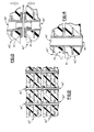
- FIGS. 12-15 there is shown yet another method of making a multilayered circuit board assembly for the invention.
- a plurality of layered subassemblies each including a plurality of through-holes therein, are independently formed and subsequently aligned (e.g. using external alignment means such as described above) such that through-holes in each of these subassemblies are aligned with respective other through-holes to form a composite having aligned holes such as illustrated in FIG. 15.
- aligned holes in each of these subassemblies are aligned with respective other through-holes to form a composite having aligned holes such as illustrated in FIG. 15.
- a composite having aligned holes such as illustrated in FIG. 15.
- only two such layered subassemblies (20", 40" in FIG. 12) are necessary.
- Each layered subassembly possesses the appropriate wiring density and resistances (e.g. such as for those in FIGS. 1-5).
- each through-hole includes an extending portion of conductive material (copper) 101 which extends from each layered subassembly and occupies a selected area on the outer surface thereof.
- extension portions, or "lands”, 101 each thus constitute a thin layer of copper material designed for aligning with a corresponding similarly sized element on the adjacent subassembly.
- each aligned subassembly is substantially similar in diameter, it is of course possible to provide holes in one of these subassemblies that are slightly larger in size, e.g., so as to produce a final structure similarly in shape and configuration to that in FIG. 11.
- a thin layer of tin is then coated onto these extending portions 101 and slightly inwardly of each through hole 35" to a prescribed depth (e.g., 3.81 /1.m (0.00015 inch)).
- Pressure e.g., in the above-mentioned amount
- elevated temperatures e.g., from about 250 C to about 300 C.
- the tin layer 103 becomes molten and, due to the pressures applied, diffuses into the copper of the extending land areas 101 to form a substantially solid structure as illustrated in FIG. 14.
- Such diffusion is represented illustratively in FIG. 14 by the removal of demarcation lines or the like between the abutting land areas 101, such abutting structure thus now represented as a homogenous structure.
- FIG. 15 In the embodiment of FIG. 15, four layered subassemblies have thus been bonded to form the composite structure thereof.
- These subsequent layered subassemblies are represented by the numerals 60" and 80", each including, preferably, the three conductive wiring layers similar to those in the previous embodiments (though possibly of greater thicknesses and/or widths and/or spacings).
- a preferred dielectric material for each of the layered subassemblies used in this embodiment is polyimide or polytetrafluoroethylene (e.g., Teflon), a known polymer material. Such a material is preferred due to the relatively high temperatures and/or pressures to which the composite is subjected during final assembly.
- FIG. 15 illustrates an equal number of through-holes in each of the layered subassemblies
- the number of through-holes per subassembly will vary and, most preferably, will progressively decrease in number from the upper, higher density layer (20") to the bottom, lesser density layer (80").
- Such additional holes may be pre-drilled in each subassembly prior to the aforedefined aligning and bonding operations.
Landscapes
- Engineering & Computer Science (AREA)
- Microelectronics & Electronic Packaging (AREA)
- Manufacturing & Machinery (AREA)
- Production Of Multi-Layered Print Wiring Board (AREA)
Applications Claiming Priority (2)
| Application Number | Priority Date | Filing Date | Title |
|---|---|---|---|
| US07/561,401 US5191174A (en) | 1990-08-01 | 1990-08-01 | High density circuit board and method of making same |
| US561401 | 1990-08-01 |
Publications (2)
| Publication Number | Publication Date |
|---|---|
| EP0469308A1 true EP0469308A1 (de) | 1992-02-05 |
| EP0469308B1 EP0469308B1 (de) | 1996-02-28 |
Family
ID=24241803
Family Applications (1)
| Application Number | Title | Priority Date | Filing Date |
|---|---|---|---|
| EP91110864A Expired - Lifetime EP0469308B1 (de) | 1990-08-01 | 1991-07-01 | Mehrschichtleiterplatte und Verfahren zu ihrer Herstellung |
Country Status (4)
| Country | Link |
|---|---|
| US (1) | US5191174A (de) |
| EP (1) | EP0469308B1 (de) |
| JP (1) | JPH0719966B2 (de) |
| DE (1) | DE69117381T2 (de) |
Cited By (7)
| Publication number | Priority date | Publication date | Assignee | Title |
|---|---|---|---|---|
| AT401131B (de) * | 1992-05-15 | 1996-06-25 | Schrack Telecom | Mehrlagen-leiterplatte |
| WO2000032021A1 (en) * | 1998-11-19 | 2000-06-02 | Alliedsignal Inc. | Printed circuit assembly having locally enhanced wiring density |
| EP1194022A1 (de) * | 1999-06-02 | 2002-04-03 | Ibiden Co., Ltd. | Mehrschichtige, gedruckte leiterplatte und herstellungsmethode für eine mehrschichtige, gedruckte leiterplatte |
| EP1487060A2 (de) * | 2003-06-12 | 2004-12-15 | Nortel Networks Limited | Verbindungstechnik für mehrlagige gedruckte Leiterplatten |
| WO2009047075A1 (de) * | 2007-10-05 | 2009-04-16 | Robert Bosch Gmbh | Verfahren und vorrichtung zur herstellung zumindest einer leiterplatte |
| CN105898982A (zh) * | 2016-06-30 | 2016-08-24 | 广东顺德施瑞科技有限公司 | 一种高压柔性线路板及多层柔性线路板 |
| CN110740591A (zh) * | 2019-10-25 | 2020-01-31 | 珠海杰赛科技有限公司 | 一种多层印制板的盲孔加工方法 |
Families Citing this family (147)
| Publication number | Priority date | Publication date | Assignee | Title |
|---|---|---|---|---|
| JP3226533B2 (ja) * | 1990-10-01 | 2001-11-05 | ソニー株式会社 | 多層配線基板及びその製造方法 |
| DE69218319T2 (de) * | 1991-07-26 | 1997-07-10 | Nec Corp., Tokio/Tokyo | Mehrschichtige Leiterplatte aus Polyimid und Verfahren zur Herstellung |
| US5397861A (en) * | 1992-10-21 | 1995-03-14 | Mupac Corporation | Electrical interconnection board |
| JP3355353B2 (ja) * | 1993-08-20 | 2002-12-09 | ケル株式会社 | 電気コネクタ |
| US5359767A (en) * | 1993-08-26 | 1994-11-01 | International Business Machines Corporation | Method of making multilayered circuit board |
| US5435480A (en) * | 1993-12-23 | 1995-07-25 | International Business Machines Corporation | Method for filling plated through holes |
| US5723823A (en) * | 1994-06-09 | 1998-03-03 | Dell Usa, L.P. | Circuit board with enhanced rework configuration |
| US6204453B1 (en) * | 1998-12-02 | 2001-03-20 | International Business Machines Corporation | Two signal one power plane circuit board |
| JP2748890B2 (ja) * | 1995-06-14 | 1998-05-13 | 日本電気株式会社 | 有機樹脂多層配線基板およびその製造方法 |
| US5736679A (en) * | 1995-12-26 | 1998-04-07 | International Business Machines Corporation | Deformable interconnect structure for connecting an internal plane to a through-hole in a multilayer circuit board |
| JP3395621B2 (ja) * | 1997-02-03 | 2003-04-14 | イビデン株式会社 | プリント配線板及びその製造方法 |
| US5847936A (en) * | 1997-06-20 | 1998-12-08 | Sun Microsystems, Inc. | Optimized routing scheme for an integrated circuit/printed circuit board |
| JP2894325B2 (ja) * | 1997-06-25 | 1999-05-24 | 日本電気株式会社 | 電子回路のシールド構造 |
| TW421980B (en) * | 1997-12-22 | 2001-02-11 | Citizen Watch Co Ltd | Electronic component device, its manufacturing process, and collective circuits |
| US6281446B1 (en) * | 1998-02-16 | 2001-08-28 | Matsushita Electric Industrial Co., Ltd. | Multi-layered circuit board and method of manufacturing the same |
| US6720501B1 (en) | 1998-04-14 | 2004-04-13 | Formfactor, Inc. | PC board having clustered blind vias |
| WO1999056508A1 (en) * | 1998-04-29 | 1999-11-04 | Compunetics, Inc. | Rigid interconnect device and method of making |
| JP3201345B2 (ja) * | 1998-05-13 | 2001-08-20 | 日本電気株式会社 | 多層プリント配線板 |
| SE513341C2 (sv) * | 1998-10-06 | 2000-08-28 | Ericsson Telefon Ab L M | Arrangemang med tryckta kretskort samt metod för tillverkning därav |
| US6175087B1 (en) * | 1998-12-02 | 2001-01-16 | International Business Machines Corporation | Composite laminate circuit structure and method of forming the same |
| US6198634B1 (en) * | 1999-03-31 | 2001-03-06 | International Business Machines Corporation | Electronic package with stacked connections |
| US6297458B1 (en) * | 1999-04-14 | 2001-10-02 | Dell Usa, L.P. | Printed circuit board and method for evaluating the inner layer hole registration process capability of the printed circuit board manufacturing process |
| JP3669219B2 (ja) * | 1999-08-10 | 2005-07-06 | 日本電気株式会社 | 多層プリント配線板 |
| US6399898B1 (en) * | 1999-11-18 | 2002-06-04 | Nortel Networks Limited | Technique for coupling signals between circuit boards |
| US6407341B1 (en) | 2000-04-25 | 2002-06-18 | International Business Machines Corporation | Conductive substructures of a multilayered laminate |
| US6589820B1 (en) | 2000-06-16 | 2003-07-08 | Micron Technology, Inc. | Method and apparatus for packaging a microelectronic die |
| US7069646B2 (en) * | 2000-06-19 | 2006-07-04 | Nortel Networks Limited | Techniques for reducing the number of layers in a multilayer signal routing device |
| US6483044B1 (en) * | 2000-08-23 | 2002-11-19 | Micron Technology, Inc. | Interconnecting substrates for electrical coupling of microelectronic components |
| US6979595B1 (en) * | 2000-08-24 | 2005-12-27 | Micron Technology, Inc. | Packaged microelectronic devices with pressure release elements and methods for manufacturing and using such packaged microelectronic devices |
| US6838760B1 (en) | 2000-08-28 | 2005-01-04 | Micron Technology, Inc. | Packaged microelectronic devices with interconnecting units |
| US6388204B1 (en) | 2000-08-29 | 2002-05-14 | International Business Machines Corporation | Composite laminate circuit structure and methods of interconnecting the same |
| US6931723B1 (en) * | 2000-09-19 | 2005-08-23 | International Business Machines Corporation | Organic dielectric electronic interconnect structures and method for making |
| TW483293B (en) * | 2000-11-10 | 2002-04-11 | Via Tech Inc | Circuit daughter board and circuit board structure for stabilizing power source and strengthening grounding |
| US6495770B2 (en) * | 2000-12-04 | 2002-12-17 | Intel Corporation | Electronic assembly providing shunting of electrical current |
| US20040108862A1 (en) * | 2001-02-19 | 2004-06-10 | Kenji Azuma | Printed wiring board, multilayer printed wiring board, and method of detecting foreign matter and voids in inner layer of multilayer printed wiring board |
| US6384341B1 (en) * | 2001-04-30 | 2002-05-07 | Tyco Electronics Corporation | Differential connector footprint for a multi-layer circuit board |
| US6504111B2 (en) | 2001-05-29 | 2003-01-07 | International Business Machines Corporation | Solid via layer to layer interconnect |
| US6930256B1 (en) | 2002-05-01 | 2005-08-16 | Amkor Technology, Inc. | Integrated circuit substrate having laser-embedded conductive patterns and method therefor |
| US6987661B1 (en) | 2001-06-19 | 2006-01-17 | Amkor Technology, Inc. | Integrated circuit substrate having embedded passive components and methods therefor |
| US7334326B1 (en) | 2001-06-19 | 2008-02-26 | Amkor Technology, Inc. | Method for making an integrated circuit substrate having embedded passive components |
| JP4917225B2 (ja) * | 2001-09-28 | 2012-04-18 | ローム株式会社 | 半導体装置 |
| US6941649B2 (en) * | 2002-02-05 | 2005-09-13 | Force10 Networks, Inc. | Method of fabricating a high-layer-count backplane |
| US6831371B1 (en) | 2002-03-16 | 2004-12-14 | Amkor Technology, Inc. | Integrated circuit substrate having embedded wire conductors and method therefor |
| US7633765B1 (en) | 2004-03-23 | 2009-12-15 | Amkor Technology, Inc. | Semiconductor package including a top-surface metal layer for implementing circuit features |
| US20080043447A1 (en) * | 2002-05-01 | 2008-02-21 | Amkor Technology, Inc. | Semiconductor package having laser-embedded terminals |
| US7548430B1 (en) | 2002-05-01 | 2009-06-16 | Amkor Technology, Inc. | Buildup dielectric and metallization process and semiconductor package |
| US7670962B2 (en) | 2002-05-01 | 2010-03-02 | Amkor Technology, Inc. | Substrate having stiffener fabrication method |
| US7399661B2 (en) * | 2002-05-01 | 2008-07-15 | Amkor Technology, Inc. | Method for making an integrated circuit substrate having embedded back-side access conductors and vias |
| US9691635B1 (en) | 2002-05-01 | 2017-06-27 | Amkor Technology, Inc. | Buildup dielectric layer having metallization pattern semiconductor package fabrication method |
| US7028400B1 (en) | 2002-05-01 | 2006-04-18 | Amkor Technology, Inc. | Integrated circuit substrate having laser-exposed terminals |
| US6930257B1 (en) | 2002-05-01 | 2005-08-16 | Amkor Technology, Inc. | Integrated circuit substrate having laminated laser-embedded circuit layers |
| US7424133B2 (en) | 2002-11-08 | 2008-09-09 | Pictometry International Corporation | Method and apparatus for capturing, geolocating and measuring oblique images |
| KR100499004B1 (ko) * | 2002-12-18 | 2005-07-01 | 삼성전기주식회사 | 광비아홀을 구비하는 인쇄회로기판 및 가공 공정 |
| US7047628B2 (en) * | 2003-01-31 | 2006-05-23 | Brocade Communications Systems, Inc. | Impedance matching of differential pair signal traces on printed wiring boards |
| US6936502B2 (en) * | 2003-05-14 | 2005-08-30 | Nortel Networks Limited | Package modification for channel-routed circuit boards |
| US6933596B2 (en) * | 2003-07-01 | 2005-08-23 | Northrop Grumman Corporation | Ultra wideband BGA |
| CN101547562A (zh) * | 2003-09-19 | 2009-09-30 | 通道系统集团公司 | 闭合反钻系统 |
| JP4401912B2 (ja) * | 2003-10-17 | 2010-01-20 | 学校法人早稲田大学 | 半導体多層配線板の形成方法 |
| US7180171B1 (en) * | 2004-01-08 | 2007-02-20 | Smart Modular Technologies, Inc. | Single IC packaging solution for multi chip modules |
| US11081370B2 (en) | 2004-03-23 | 2021-08-03 | Amkor Technology Singapore Holding Pte. Ltd. | Methods of manufacturing an encapsulated semiconductor device |
| US10811277B2 (en) | 2004-03-23 | 2020-10-20 | Amkor Technology, Inc. | Encapsulated semiconductor package |
| US7145238B1 (en) | 2004-05-05 | 2006-12-05 | Amkor Technology, Inc. | Semiconductor package and substrate having multi-level vias |
| FR2877805B1 (fr) * | 2004-11-09 | 2007-03-16 | Sagem | Dispositif de filtrage d'interferences electromagnetiques pour un boitier metallique contenant du materiel electronique, et boitier metallique qui en est equipe |
| US7307437B1 (en) * | 2005-03-24 | 2007-12-11 | Hewlett-Packard Development Company, L.P. | Arrangement with conductive pad embedment |
| US8826531B1 (en) | 2005-04-05 | 2014-09-09 | Amkor Technology, Inc. | Method for making an integrated circuit substrate having laminated laser-embedded circuit layers |
| US20060261498A1 (en) * | 2005-05-17 | 2006-11-23 | Micron Technology, Inc. | Methods and apparatuses for encapsulating microelectronic devices |
| JP4682028B2 (ja) * | 2005-11-28 | 2011-05-11 | Hoya株式会社 | 導電層の製造方法、導電層、及び、信号伝送基板 |
| JP2007194423A (ja) * | 2006-01-19 | 2007-08-02 | Hitachi Ltd | プリント配線板のスルーホール構造及びプリント配線板 |
| JP2007311990A (ja) * | 2006-05-17 | 2007-11-29 | Pentax Corp | 通信装置 |
| US7873238B2 (en) | 2006-08-30 | 2011-01-18 | Pictometry International Corporation | Mosaic oblique images and methods of making and using same |
| US7589398B1 (en) | 2006-10-04 | 2009-09-15 | Amkor Technology, Inc. | Embedded metal features structure |
| US7550857B1 (en) | 2006-11-16 | 2009-06-23 | Amkor Technology, Inc. | Stacked redistribution layer (RDL) die assembly package |
| US7750250B1 (en) | 2006-12-22 | 2010-07-06 | Amkor Technology, Inc. | Blind via capture pad structure |
| US7608538B2 (en) * | 2007-01-05 | 2009-10-27 | International Business Machines Corporation | Formation of vertical devices by electroplating |
| US7752752B1 (en) | 2007-01-09 | 2010-07-13 | Amkor Technology, Inc. | Method of fabricating an embedded circuit pattern |
| US8593518B2 (en) * | 2007-02-01 | 2013-11-26 | Pictometry International Corp. | Computer system for continuous oblique panning |
| US8520079B2 (en) * | 2007-02-15 | 2013-08-27 | Pictometry International Corp. | Event multiplexer for managing the capture of images |
| US7833456B2 (en) * | 2007-02-23 | 2010-11-16 | Micron Technology, Inc. | Systems and methods for compressing an encapsulant adjacent a semiconductor workpiece |
| US8385672B2 (en) * | 2007-05-01 | 2013-02-26 | Pictometry International Corp. | System for detecting image abnormalities |
| US9262818B2 (en) | 2007-05-01 | 2016-02-16 | Pictometry International Corp. | System for detecting image abnormalities |
| US8323771B1 (en) | 2007-08-15 | 2012-12-04 | Amkor Technology, Inc. | Straight conductor blind via capture pad structure and fabrication method |
| US7991226B2 (en) | 2007-10-12 | 2011-08-02 | Pictometry International Corporation | System and process for color-balancing a series of oblique images |
| US8531472B2 (en) | 2007-12-03 | 2013-09-10 | Pictometry International Corp. | Systems and methods for rapid three-dimensional modeling with real façade texture |
| US8588547B2 (en) | 2008-08-05 | 2013-11-19 | Pictometry International Corp. | Cut-line steering methods for forming a mosaic image of a geographical area |
| US20100159193A1 (en) * | 2008-12-18 | 2010-06-24 | Palo Alto Research Center Incorporated | Combined electrical and fluidic interconnect via structure |
| US8872329B1 (en) | 2009-01-09 | 2014-10-28 | Amkor Technology, Inc. | Extended landing pad substrate package structure and method |
| US7960827B1 (en) | 2009-04-09 | 2011-06-14 | Amkor Technology, Inc. | Thermal via heat spreader package and method |
| US8401222B2 (en) | 2009-05-22 | 2013-03-19 | Pictometry International Corp. | System and process for roof measurement using aerial imagery |
| US8623753B1 (en) | 2009-05-28 | 2014-01-07 | Amkor Technology, Inc. | Stackable protruding via package and method |
| US8222538B1 (en) | 2009-06-12 | 2012-07-17 | Amkor Technology, Inc. | Stackable via package and method |
| US8471154B1 (en) | 2009-08-06 | 2013-06-25 | Amkor Technology, Inc. | Stackable variable height via package and method |
| US8796561B1 (en) | 2009-10-05 | 2014-08-05 | Amkor Technology, Inc. | Fan out build up substrate stackable package and method |
| US9330494B2 (en) | 2009-10-26 | 2016-05-03 | Pictometry International Corp. | Method for the automatic material classification and texture simulation for 3D models |
| US8937381B1 (en) | 2009-12-03 | 2015-01-20 | Amkor Technology, Inc. | Thin stackable package and method |
| US9691734B1 (en) | 2009-12-07 | 2017-06-27 | Amkor Technology, Inc. | Method of forming a plurality of electronic component packages |
| US8536462B1 (en) | 2010-01-22 | 2013-09-17 | Amkor Technology, Inc. | Flex circuit package and method |
| US8300423B1 (en) | 2010-05-25 | 2012-10-30 | Amkor Technology, Inc. | Stackable treated via package and method |
| US8294276B1 (en) | 2010-05-27 | 2012-10-23 | Amkor Technology, Inc. | Semiconductor device and fabricating method thereof |
| US8477190B2 (en) | 2010-07-07 | 2013-07-02 | Pictometry International Corp. | Real-time moving platform management system |
| US8338229B1 (en) | 2010-07-30 | 2012-12-25 | Amkor Technology, Inc. | Stackable plasma cleaned via package and method |
| US8717775B1 (en) | 2010-08-02 | 2014-05-06 | Amkor Technology, Inc. | Fingerprint sensor package and method |
| KR20120017245A (ko) * | 2010-08-18 | 2012-02-28 | 삼성전기주식회사 | 인쇄회로기판 및 이의 제조방법 |
| TW201218891A (en) * | 2010-10-18 | 2012-05-01 | Hon Hai Prec Ind Co Ltd | Printed circuit board |
| CN102458034A (zh) * | 2010-10-19 | 2012-05-16 | 鸿富锦精密工业(深圳)有限公司 | 印刷电路板 |
| DE102010049499B4 (de) * | 2010-10-27 | 2014-04-10 | Curamik Electronics Gmbh | Metall-Keramik-Substrat sowie Verfahren zum Herstellen eines solchen Substrates |
| US8337657B1 (en) | 2010-10-27 | 2012-12-25 | Amkor Technology, Inc. | Mechanical tape separation package and method |
| US8482134B1 (en) | 2010-11-01 | 2013-07-09 | Amkor Technology, Inc. | Stackable package and method |
| US9748154B1 (en) | 2010-11-04 | 2017-08-29 | Amkor Technology, Inc. | Wafer level fan out semiconductor device and manufacturing method thereof |
| US8525318B1 (en) | 2010-11-10 | 2013-09-03 | Amkor Technology, Inc. | Semiconductor device and fabricating method thereof |
| US8557629B1 (en) | 2010-12-03 | 2013-10-15 | Amkor Technology, Inc. | Semiconductor device having overlapped via apertures |
| US8535961B1 (en) | 2010-12-09 | 2013-09-17 | Amkor Technology, Inc. | Light emitting diode (LED) package and method |
| US8823732B2 (en) | 2010-12-17 | 2014-09-02 | Pictometry International Corp. | Systems and methods for processing images with edge detection and snap-to feature |
| US9721872B1 (en) | 2011-02-18 | 2017-08-01 | Amkor Technology, Inc. | Methods and structures for increasing the allowable die size in TMV packages |
| US9013011B1 (en) | 2011-03-11 | 2015-04-21 | Amkor Technology, Inc. | Stacked and staggered die MEMS package and method |
| KR101140113B1 (ko) | 2011-04-26 | 2012-04-30 | 앰코 테크놀로지 코리아 주식회사 | 반도체 디바이스 |
| WO2013106080A2 (en) | 2011-06-10 | 2013-07-18 | Pictometry International Corp. | System and method for forming a video stream containing gis data in real-time |
| US8653674B1 (en) | 2011-09-15 | 2014-02-18 | Amkor Technology, Inc. | Electronic component package fabrication method and structure |
| US8633598B1 (en) | 2011-09-20 | 2014-01-21 | Amkor Technology, Inc. | Underfill contacting stacking balls package fabrication method and structure |
| US8904632B2 (en) | 2011-09-23 | 2014-12-09 | Harris Corporation | Method to make a multilayer circuit board with intermetallic compound and related circuit boards |
| US9029962B1 (en) | 2011-10-12 | 2015-05-12 | Amkor Technology, Inc. | Molded cavity substrate MEMS package fabrication method and structure |
| JP5628772B2 (ja) * | 2011-10-20 | 2014-11-19 | 日立オートモティブシステムズ株式会社 | プリント基板およびそれを用いた電子機器 |
| TWI449152B (zh) | 2011-12-21 | 2014-08-11 | Ind Tech Res Inst | 半導體元件堆疊結構 |
| US20130196539A1 (en) * | 2012-01-12 | 2013-08-01 | John Mezzalingua Associates, Inc. | Electronics Packaging Assembly with Dielectric Cover |
| US9183538B2 (en) | 2012-03-19 | 2015-11-10 | Pictometry International Corp. | Method and system for quick square roof reporting |
| US9799592B2 (en) | 2013-11-19 | 2017-10-24 | Amkor Technology, Inc. | Semicondutor device with through-silicon via-less deep wells |
| KR101366461B1 (ko) | 2012-11-20 | 2014-02-26 | 앰코 테크놀로지 코리아 주식회사 | 반도체 디바이스 및 그 제조 방법 |
| US9545003B2 (en) * | 2012-12-28 | 2017-01-10 | Fci Americas Technology Llc | Connector footprints in printed circuit board (PCB) |
| US9244272B2 (en) | 2013-03-12 | 2016-01-26 | Pictometry International Corp. | Lidar system producing multiple scan paths and method of making and using same |
| US9881163B2 (en) | 2013-03-12 | 2018-01-30 | Pictometry International Corp. | System and method for performing sensitive geo-spatial processing in non-sensitive operator environments |
| US9538636B1 (en) * | 2013-03-14 | 2017-01-03 | Macom Technology Solutions Holdings, Inc. | Blind via edge castellation |
| US9275080B2 (en) | 2013-03-15 | 2016-03-01 | Pictometry International Corp. | System and method for early access to captured images |
| US9753950B2 (en) | 2013-03-15 | 2017-09-05 | Pictometry International Corp. | Virtual property reporting for automatic structure detection |
| KR101488590B1 (ko) | 2013-03-29 | 2015-01-30 | 앰코 테크놀로지 코리아 주식회사 | 반도체 디바이스 및 그 제조 방법 |
| JP6061195B2 (ja) * | 2013-04-05 | 2017-01-18 | 幸弘 西村 | ブレーキによる点灯制御機能をもった自転車用ライト装置 |
| KR101607981B1 (ko) | 2013-11-04 | 2016-03-31 | 앰코 테크놀로지 코리아 주식회사 | 반도체 패키지용 인터포저 및 이의 제조 방법, 제조된 인터포저를 이용한 반도체 패키지 |
| EP3435188B1 (de) | 2014-01-10 | 2021-11-10 | Pictometry International Corp. | System und verfahren zur strukturbeurteilung mittels eines unbemannten luftfahrzeugs |
| US9292913B2 (en) | 2014-01-31 | 2016-03-22 | Pictometry International Corp. | Augmented three dimensional point collection of vertical structures |
| CA2938973A1 (en) | 2014-02-08 | 2015-08-13 | Pictometry International Corp. | Method and system for displaying room interiors on a floor plan |
| WO2017120571A1 (en) | 2016-01-08 | 2017-07-13 | Pictometry International Corp. | Systems and methods for taking, processing, retrieving, and displaying images from unmanned aerial vehicles |
| WO2017142788A1 (en) | 2016-02-15 | 2017-08-24 | Pictometry International Corp. | Automated system and methodology for feature extraction |
| US10671648B2 (en) | 2016-02-22 | 2020-06-02 | Eagle View Technologies, Inc. | Integrated centralized property database systems and methods |
| US9960328B2 (en) | 2016-09-06 | 2018-05-01 | Amkor Technology, Inc. | Semiconductor device and manufacturing method thereof |
| US10999939B2 (en) * | 2018-06-08 | 2021-05-04 | Unimicron Technology Corp. | Circuit carrier board and manufacturing method thereof |
| US10892213B2 (en) * | 2018-12-28 | 2021-01-12 | Advanced Semiconductor Engineering, Inc. | Wiring structure and method for manufacturing the same |
| US11690177B2 (en) | 2020-04-07 | 2023-06-27 | Nextgin Technology Bv | Methods and systems for back-drilling a multi-layer circuit board |
| US11355426B2 (en) * | 2020-07-31 | 2022-06-07 | Advanced Semiconductor Engineering, Inc. | Wiring structure and method for manufacturing the same |
| CN113594129A (zh) * | 2021-07-20 | 2021-11-02 | 日月光半导体制造股份有限公司 | 半导体封装装置及其制造方法 |
Citations (3)
| Publication number | Priority date | Publication date | Assignee | Title |
|---|---|---|---|---|
| US4710854A (en) * | 1985-03-27 | 1987-12-01 | Hitachi, Ltd. | Hybrid multilayer wiring board |
| US4788766A (en) * | 1987-05-20 | 1988-12-06 | Loral Corporation | Method of fabricating a multilayer circuit board assembly |
| US4854038A (en) * | 1988-03-16 | 1989-08-08 | International Business Machines Corporation | Modularized fabrication of high performance printed circuit boards |
Family Cites Families (6)
| Publication number | Priority date | Publication date | Assignee | Title |
|---|---|---|---|---|
| US3436819A (en) * | 1965-09-22 | 1969-04-08 | Litton Systems Inc | Multilayer laminate |
| US3516156A (en) * | 1967-12-11 | 1970-06-23 | Ibm | Circuit package assembly process |
| JPH0716094B2 (ja) * | 1986-03-31 | 1995-02-22 | 日立化成工業株式会社 | 配線板の製造法 |
| JPS63249394A (ja) * | 1987-04-06 | 1988-10-17 | 日本電気株式会社 | 多層回路基板 |
| US4803450A (en) * | 1987-12-14 | 1989-02-07 | General Electric Company | Multilayer circuit board fabricated from silicon |
| US4967314A (en) * | 1988-03-28 | 1990-10-30 | Prime Computer Inc. | Circuit board construction |
-
1990
- 1990-08-01 US US07/561,401 patent/US5191174A/en not_active Expired - Lifetime
-
1991
- 1991-07-01 EP EP91110864A patent/EP0469308B1/de not_active Expired - Lifetime
- 1991-07-01 DE DE69117381T patent/DE69117381T2/de not_active Expired - Fee Related
- 1991-07-18 JP JP3202240A patent/JPH0719966B2/ja not_active Expired - Lifetime
Patent Citations (3)
| Publication number | Priority date | Publication date | Assignee | Title |
|---|---|---|---|---|
| US4710854A (en) * | 1985-03-27 | 1987-12-01 | Hitachi, Ltd. | Hybrid multilayer wiring board |
| US4788766A (en) * | 1987-05-20 | 1988-12-06 | Loral Corporation | Method of fabricating a multilayer circuit board assembly |
| US4854038A (en) * | 1988-03-16 | 1989-08-08 | International Business Machines Corporation | Modularized fabrication of high performance printed circuit boards |
Cited By (20)
| Publication number | Priority date | Publication date | Assignee | Title |
|---|---|---|---|---|
| AT401131B (de) * | 1992-05-15 | 1996-06-25 | Schrack Telecom | Mehrlagen-leiterplatte |
| WO2000032021A1 (en) * | 1998-11-19 | 2000-06-02 | Alliedsignal Inc. | Printed circuit assembly having locally enhanced wiring density |
| US8822828B2 (en) | 1999-06-02 | 2014-09-02 | Ibiden Co., Ltd. | Multi-layer printed circuit board and method of manufacturing multi-layer printed circuit board |
| EP1194022A1 (de) * | 1999-06-02 | 2002-04-03 | Ibiden Co., Ltd. | Mehrschichtige, gedruckte leiterplatte und herstellungsmethode für eine mehrschichtige, gedruckte leiterplatte |
| US6828510B1 (en) | 1999-06-02 | 2004-12-07 | Ibiden Co., Ltd. | Multilayer printed wiring board and method of manufacturing multilayer printed wiring board |
| US8822830B2 (en) | 1999-06-02 | 2014-09-02 | Ibiden Co., Ltd. | Multi-layer printed circuit board and method of manufacturing multi-layer printed circuit board |
| EP1194022A4 (de) * | 1999-06-02 | 2004-03-17 | Ibiden Co Ltd | Mehrschichtige, gedruckte leiterplatte und herstellungsmethode für eine mehrschichtige, gedruckte leiterplatte |
| US8782882B2 (en) | 1999-06-02 | 2014-07-22 | Ibiden Co., Ltd. | Method of manufacturing multi-layer printed circuit board |
| EP2086299A1 (de) * | 1999-06-02 | 2009-08-05 | Ibiden Co., Ltd. | Mehrschichtige bestückte Leiterplatte und Verfahren zur Herstellung einer mehrschichtigen bestückten Leiterplatte |
| US7985930B2 (en) | 1999-06-02 | 2011-07-26 | Ibiden Co., Ltd. | Multi-layer printed circuit board and method of manufacturing multi-layer printed circuit board |
| US8283573B2 (en) | 1999-06-02 | 2012-10-09 | Ibiden Co., Ltd. | Multi-layer printed circuit board and method of manufacturing multilayer printed circuit board |
| US8288665B2 (en) | 1999-06-02 | 2012-10-16 | Ibiden Co., Ltd. | Multi-layer printed circuit board and method of manufacturing multi-layer printed circuit board |
| US8288664B2 (en) | 1999-06-02 | 2012-10-16 | Ibiden Co., Ltd. | Multi-layer printed circuit board and method of manufacturing multilayer printed circuit board |
| US8745863B2 (en) | 1999-06-02 | 2014-06-10 | Ibiden Co., Ltd. | Method of manufacturing multi-layer printed circuit board |
| EP1487060A3 (de) * | 2003-06-12 | 2007-11-07 | Nortel Networks Limited | Verbindungstechnik für mehrlagige gedruckte Leiterplatten |
| EP1487060A2 (de) * | 2003-06-12 | 2004-12-15 | Nortel Networks Limited | Verbindungstechnik für mehrlagige gedruckte Leiterplatten |
| WO2009047075A1 (de) * | 2007-10-05 | 2009-04-16 | Robert Bosch Gmbh | Verfahren und vorrichtung zur herstellung zumindest einer leiterplatte |
| CN105898982A (zh) * | 2016-06-30 | 2016-08-24 | 广东顺德施瑞科技有限公司 | 一种高压柔性线路板及多层柔性线路板 |
| CN110740591A (zh) * | 2019-10-25 | 2020-01-31 | 珠海杰赛科技有限公司 | 一种多层印制板的盲孔加工方法 |
| CN110740591B (zh) * | 2019-10-25 | 2021-06-25 | 珠海杰赛科技有限公司 | 一种多层印制板的盲孔加工方法 |
Also Published As
| Publication number | Publication date |
|---|---|
| DE69117381D1 (de) | 1996-04-04 |
| JPH0719966B2 (ja) | 1995-03-06 |
| EP0469308B1 (de) | 1996-02-28 |
| JPH04233794A (ja) | 1992-08-21 |
| US5191174A (en) | 1993-03-02 |
| DE69117381T2 (de) | 1996-09-26 |
Similar Documents
| Publication | Publication Date | Title |
|---|---|---|
| US5191174A (en) | High density circuit board and method of making same | |
| US5770476A (en) | Passive interposer including at least one passive electronic component | |
| US7402758B2 (en) | Telescoping blind via in three-layer core | |
| US5829124A (en) | Method for forming metallized patterns on the top surface of a printed circuit board | |
| US6687985B2 (en) | Method of Manufacturing a multi-layer circuit board | |
| KR100442215B1 (ko) | 인쇄배선회로다층어셈블리및그제조방법 | |
| US5004639A (en) | Rigid flex printed circuit configuration | |
| US6541712B1 (en) | High speed multi-layer printed circuit board via | |
| US5736679A (en) | Deformable interconnect structure for connecting an internal plane to a through-hole in a multilayer circuit board | |
| US5038252A (en) | Printed circuit boards with improved electrical current control | |
| US5428190A (en) | Rigid-flex board with anisotropic interconnect and method of manufacture | |
| US4543715A (en) | Method of forming vertical traces on printed circuit board | |
| KR940009175B1 (ko) | 다층 프린트기판의 제조방법 | |
| US5440805A (en) | Method of manufacturing a multilayer circuit | |
| US4030190A (en) | Method for forming a multilayer printed circuit board | |
| US4170819A (en) | Method of making conductive via holes in printed circuit boards | |
| US20090241332A1 (en) | Circuitized substrate and method of making same | |
| US20080277154A1 (en) | Process for making stubless printed circuit boards | |
| US6147870A (en) | Printed circuit assembly having locally enhanced wiring density | |
| EP0332834A1 (de) | Leiterplatten mit niedriger Dielektrizitätskonstante | |
| US5637834A (en) | Multilayer circuit substrate and method for forming same | |
| US5245135A (en) | Stackable high density interconnection mechanism (SHIM) | |
| US20090178273A1 (en) | Method of making circuitized assembly including a plurality of circuitized substrates | |
| EP0451541B1 (de) | Herstellung von mehrschichtigen Leiterplatten mit erhöhter Leiterbahnendichte | |
| JPH11145628A (ja) | 印刷配線基板 |
Legal Events
| Date | Code | Title | Description |
|---|---|---|---|
| PUAI | Public reference made under article 153(3) epc to a published international application that has entered the european phase |
Free format text: ORIGINAL CODE: 0009012 |
|
| AK | Designated contracting states |
Kind code of ref document: A1 Designated state(s): DE FR GB |
|
| 17P | Request for examination filed |
Effective date: 19920619 |
|
| 17Q | First examination report despatched |
Effective date: 19931027 |
|
| GRAA | (expected) grant |
Free format text: ORIGINAL CODE: 0009210 |
|
| AK | Designated contracting states |
Kind code of ref document: B1 Designated state(s): DE FR GB |
|
| REF | Corresponds to: |
Ref document number: 69117381 Country of ref document: DE Date of ref document: 19960404 |
|
| ET | Fr: translation filed | ||
| PGFP | Annual fee paid to national office [announced via postgrant information from national office to epo] |
Ref country code: GB Payment date: 19960621 Year of fee payment: 6 |
|
| PLBE | No opposition filed within time limit |
Free format text: ORIGINAL CODE: 0009261 |
|
| STAA | Information on the status of an ep patent application or granted ep patent |
Free format text: STATUS: NO OPPOSITION FILED WITHIN TIME LIMIT |
|
| 26N | No opposition filed | ||
| PG25 | Lapsed in a contracting state [announced via postgrant information from national office to epo] |
Ref country code: FR Effective date: 19970328 |
|
| PG25 | Lapsed in a contracting state [announced via postgrant information from national office to epo] |
Ref country code: DE Effective date: 19970402 |
|
| REG | Reference to a national code |
Ref country code: FR Ref legal event code: ST |
|
| PG25 | Lapsed in a contracting state [announced via postgrant information from national office to epo] |
Ref country code: GB Free format text: LAPSE BECAUSE OF NON-PAYMENT OF DUE FEES Effective date: 19970701 |
|
| GBPC | Gb: european patent ceased through non-payment of renewal fee |
Effective date: 19970701 |