EP0393089B1 - Repondeur - Google Patents
Repondeur Download PDFInfo
- Publication number
- EP0393089B1 EP0393089B1 EP88909960A EP88909960A EP0393089B1 EP 0393089 B1 EP0393089 B1 EP 0393089B1 EP 88909960 A EP88909960 A EP 88909960A EP 88909960 A EP88909960 A EP 88909960A EP 0393089 B1 EP0393089 B1 EP 0393089B1
- Authority
- EP
- European Patent Office
- Prior art keywords
- transponder
- inductive
- signal
- coil
- current
- Prior art date
- Legal status (The legal status is an assumption and is not a legal conclusion. Google has not performed a legal analysis and makes no representation as to the accuracy of the status listed.)
- Expired - Lifetime
Links
Images


Classifications
-
- H—ELECTRICITY
- H04—ELECTRIC COMMUNICATION TECHNIQUE
- H04B—TRANSMISSION
- H04B5/00—Near-field transmission systems, e.g. inductive or capacitive transmission systems
- H04B5/20—Near-field transmission systems, e.g. inductive or capacitive transmission systems characterised by the transmission technique; characterised by the transmission medium
- H04B5/22—Capacitive coupling
-
- G—PHYSICS
- G06—COMPUTING OR CALCULATING; COUNTING
- G06K—GRAPHICAL DATA READING; PRESENTATION OF DATA; RECORD CARRIERS; HANDLING RECORD CARRIERS
- G06K19/00—Record carriers for use with machines and with at least a part designed to carry digital markings
- G06K19/06—Record carriers for use with machines and with at least a part designed to carry digital markings characterised by the kind of the digital marking, e.g. shape, nature, code
- G06K19/067—Record carriers with conductive marks, printed circuits or semiconductor circuit elements, e.g. credit or identity cards also with resonating or responding marks without active components
- G06K19/07—Record carriers with conductive marks, printed circuits or semiconductor circuit elements, e.g. credit or identity cards also with resonating or responding marks without active components with integrated circuit chips
- G06K19/0723—Record carriers with conductive marks, printed circuits or semiconductor circuit elements, e.g. credit or identity cards also with resonating or responding marks without active components with integrated circuit chips the record carrier comprising an arrangement for non-contact communication, e.g. wireless communication circuits on transponder cards, non-contact smart cards or RFIDs
-
- G—PHYSICS
- G06—COMPUTING OR CALCULATING; COUNTING
- G06K—GRAPHICAL DATA READING; PRESENTATION OF DATA; RECORD CARRIERS; HANDLING RECORD CARRIERS
- G06K19/00—Record carriers for use with machines and with at least a part designed to carry digital markings
- G06K19/06—Record carriers for use with machines and with at least a part designed to carry digital markings characterised by the kind of the digital marking, e.g. shape, nature, code
- G06K19/067—Record carriers with conductive marks, printed circuits or semiconductor circuit elements, e.g. credit or identity cards also with resonating or responding marks without active components
- G06K19/07—Record carriers with conductive marks, printed circuits or semiconductor circuit elements, e.g. credit or identity cards also with resonating or responding marks without active components with integrated circuit chips
- G06K19/077—Constructional details, e.g. mounting of circuits in the carrier
- G06K19/07749—Constructional details, e.g. mounting of circuits in the carrier the record carrier being capable of non-contact communication, e.g. constructional details of the antenna of a non-contact smart card
- G06K19/07773—Antenna details
- G06K19/07775—Antenna details the antenna being on-chip
-
- G—PHYSICS
- G06—COMPUTING OR CALCULATING; COUNTING
- G06K—GRAPHICAL DATA READING; PRESENTATION OF DATA; RECORD CARRIERS; HANDLING RECORD CARRIERS
- G06K19/00—Record carriers for use with machines and with at least a part designed to carry digital markings
- G06K19/06—Record carriers for use with machines and with at least a part designed to carry digital markings characterised by the kind of the digital marking, e.g. shape, nature, code
- G06K19/067—Record carriers with conductive marks, printed circuits or semiconductor circuit elements, e.g. credit or identity cards also with resonating or responding marks without active components
- G06K19/07—Record carriers with conductive marks, printed circuits or semiconductor circuit elements, e.g. credit or identity cards also with resonating or responding marks without active components with integrated circuit chips
- G06K19/077—Constructional details, e.g. mounting of circuits in the carrier
- G06K19/07749—Constructional details, e.g. mounting of circuits in the carrier the record carrier being capable of non-contact communication, e.g. constructional details of the antenna of a non-contact smart card
- G06K19/07773—Antenna details
- G06K19/07777—Antenna details the antenna being of the inductive type
- G06K19/07779—Antenna details the antenna being of the inductive type the inductive antenna being a coil
-
- G—PHYSICS
- G06—COMPUTING OR CALCULATING; COUNTING
- G06K—GRAPHICAL DATA READING; PRESENTATION OF DATA; RECORD CARRIERS; HANDLING RECORD CARRIERS
- G06K7/00—Methods or arrangements for sensing record carriers, e.g. for reading patterns
- G06K7/0008—General problems related to the reading of electronic memory record carriers, independent of its reading method, e.g. power transfer
-
- G—PHYSICS
- G08—SIGNALLING
- G08G—TRAFFIC CONTROL SYSTEMS
- G08G1/00—Traffic control systems for road vehicles
- G08G1/01—Detecting movement of traffic to be counted or controlled
- G08G1/017—Detecting movement of traffic to be counted or controlled identifying vehicles
-
- H—ELECTRICITY
- H04—ELECTRIC COMMUNICATION TECHNIQUE
- H04B—TRANSMISSION
- H04B5/00—Near-field transmission systems, e.g. inductive or capacitive transmission systems
- H04B5/20—Near-field transmission systems, e.g. inductive or capacitive transmission systems characterised by the transmission technique; characterised by the transmission medium
- H04B5/24—Inductive coupling
- H04B5/26—Inductive coupling using coils
- H04B5/266—One coil at each side, e.g. with primary and secondary coils
-
- H—ELECTRICITY
- H04—ELECTRIC COMMUNICATION TECHNIQUE
- H04B—TRANSMISSION
- H04B5/00—Near-field transmission systems, e.g. inductive or capacitive transmission systems
- H04B5/40—Near-field transmission systems, e.g. inductive or capacitive transmission systems characterised by components specially adapted for near-field transmission
- H04B5/45—Transponders
Definitions
- the present invention relates to electronic and inductive communication apparatus. Specifically, the present invention relates to a transponder, more particularly, a passive transponder.
- the passive transponder may be inductively powered and may store information or perform electronic functions when it is so powered.
- the transponder of the present invention relates to a portable, integrated and relatively cheap apparatus advantageously adapted for interrogation and/or identification of an article with which the transponder is associated.
- the transponder of the present invention advantageously utilises a single coil transmission and reception system.
- the unique circuit arrangement(s) of the present invention provides a single component rectifying means.
- the present invention lends itself to integration in a single chip form.
- the means used to receive a power providing signal may also be used to transmit another signal, the reception and transmission occurring in a simultaneous manner.
- U.S. Patent specification 3,859,624 discloses two types of transponder used within an identification tag system.
- One form of the transponder disclosed therein includes an inductive powering field receiving coil and a separate coplanar coded information field generator coil.
- the power receiving coil has associated therewith a rectifier, regulator and energy storage device.
- the separate information coil is used as a transmitter means to an interrogation station. Each coil operates independently of the other.
- the identification tag system further includes an interrogation station comprising an inductive power field generator, for the first type of tag discussed above, and an information code receiver.
- the interrogation station disclosed utilises a unitary coil for both the power field generation and the coded information receiver.
- the interrogator means operates in a sequential and cyclic fashion.
- a first mode comprises AC power (inductive) generation by the interrogator for a finite time.
- a second mode during which no AC (inductive) power is radiated to the transponder, the interrogator operates as a receiver to receive a coded information signal for a finite time. These modes are performed continuously and sequentially. No disclosure exists of simultaneous power and data reception with data transmission.
- the crucial point is that the current induced in the transponder's tuned circuit, by the interrogator, generates the reply signal that carries data back to the interrogator.
- the "carrier" frequency for this data signal is almost invariably the same as the interrogator's power signal.
- a number of disclosures rely upon the generation of sub-harmonic currents, by a suitable switch means, from the current induced in the transponder's tuned circuit, i.e. Harris U.S. 2,979,321 and Sellers U.S. 4,314,373 which cannot operate with fewer than two tuned circuits. Once again the actual current in the transponder's tuned circuit directly generates the transmission signal for carrying data.
- the distinctive difference is that the carrier signal is not injected into the pickup coil. This limits the transmission signal to be the same frequency or a sub-harmonic of the interrogation signal and precludes the simultaneous reception and transmission of data by the transponder's tuned circuit.
- U.S. 4,040,053 relates to a microwave system, Power is transmitted in high frequency pulses.
- the pulse frequency is used as the timebase reference for the transponders internal logic. Without the pulses the transponder's internal logic cannot be clocked.
- the present invention can either directly use the period of the power field as a clock reference or, in a preferred form, derive the clock from an internal oscillator. If the external interrogation signal is momentarily absent proper clock signals will still be generated by the oscillator.
- the reply transmission can only occur during the interrogator's power phase. When the pulse is absent no reply carrier is generated. This reply carrier frequency is fixed at a preset harmonic of the interrogation frequency and cannot be varied at will. Data cannot be transmitted to the transponder because the circuit uses the pulse signals to clock the internal logic. All data is preprogrammed onto the transponder.
- FSK signalling results in a far wider spectral spread on the transmitted data than direct modulation (BPSK or QPSK for example) used by the present invention.
- the two FSK carriers are envelope modulated by the data and data.complement respectively.
- the data spectrum convolves with each FSK carrier.
- the total data stream bandwidth is double that of any single carrier system. The extra bandwidth required to receive the data signal degrades the systems noise and interference performance.
- a data signal is transmitted from the PIT using two open collector output stages each with a series current limiting resistor in their respective collector circuits. These resistors are connected to opposite sides of the PIT.
- the transistors are driven with complimentary signals and are driven hard "on” forcing them to act as switches.
- the resistors serve to limit the current flow from the PIT.
- the dual complimentary drive stage is provided to force signal currents through the PIT coil. Proper operation of this output driver stage is dependent upon two factors, namely the bridge rectifier being connected across the PIT, and the carrier frequency being less than the powering frequency.
- the bridge rectifier operates to ensure that the voltage between each side of the PIT and Vss is either zero or greater than zero.
- the bridge connects alternate sides of the coil to Vss and Vdd respectively.
- the voltage on the coil side connected to Vdd is a half sinewave.
- the currents drawn through 4R1 and 4R2 are likewise half sinewaves.
- the total current through the PIT consists of half sinewave pulses directed through whichever output resistor (4R1, 4R2) is active.
- the signal current through the PIT consists of a burst of half sine current pulses through 4R1 followed by a burst of half sine current pulses through 4R2. The period of these bursts being determined by the period of the keying frequency.
- the present invention may inject any frequency(s) of current (both higher or lower than the power field's frequency) without any modulation, amplitude or otherwise, of the injected current due to the voltage induced in the antenna coil by the powering field. Any choice of transmission modulation (amplitude, FSK, phase etc.) can be used with complete disregard for the interrogation signal.
- the external bridge rectifier and series connected resistors (4R1, 4R2) of U.S. 4,730,188 are crucial to the operation of that transponders communication channel. Neither of these components have been disclosed in an integrated form nor in a readily integratable form.
- the rectifier and current source advantageously used in the present invention lend themselves to integration within a fully customised integrated circuit.
- the transponder outputs are transistor switches that "sink" current through their respective series collector resistors.
- the output stage is not a current source, a current source being an element which constrains the current independently of the voltage across it.
- the output current is grossly affected by the PIT voltage, i.e. heavily amplitude modulated.
- the series collector resistors provide the only current restricting function.
- the circuit is incapable of envelope shaping the data transmission bandwidth to bandlimit the transmission signal.
- the maximum voltage at any part of the PIT coil is (Vdd - Vss) i.e. peak pickup voltage. Whereas the voltage point in the present invention has a voltage of twice the peak voltage. This is ideally suited as a programming voltage for electrically erasable memory (EEPROM) which requires a high programming voltage.
- EEPROM electrically erasable memory
- the circuit of the present invention automatically supplies this high programming voltage if it is required.
- U.S. 4,730,188 requires the carrier signal to be present for the generation of the data transmission.
- the present invention not only does not require the power signal to generate the information transmission signal, but can transmit the signal with and independently of the powering signal.
- U.S. 4,724,427 presents a diagram in which the transponder antenna and circuitry are incorporated onto a single chip. While such a small transponder would find many uses it suffers from the deficiency of not being reprogrammable "on the fly” ie while being interrogated.
- US 4,630,044 discloses a device having the pre-characterising features of claim 1.
- An object of the present invention is to provide a transponder which includes a single coil adapted for simultaneous inductive power field reception and code information transmission.
- a further object of the present invention is to provide a disposable transponder, or code tag.
- a further object of the present invention is to provide a transponder which has reduced interference capabilities with another transponder, when both transponders simultaneously transmit an information code to an interrogation station.
- Another object of the present invention is to provide a transponder in which the electronic circuitry therefor is adapted for substantially complete integration to a single (IC) chip form.
- Another object of the present invention is to provide a transponder which includes a unique power receiving and information transmitting coil structure and/or minimum configuration rectification and energy storage devices.
- Yet another object of the present invention is to provide a device which allows data receiving simultaneously with power receiving and information transmission.
- an object of the present invention is to provide a transponder which alleviates or does not suffer any one of or all the disadvantages of the prior art.
- the present invention provides a device as set out in claim 1.
- Rectifier means is coupled between one side of said inductive means and a point of reference potential.
- Said inductive and rectifier means may be operatively coupled to provide a powering voltage at another side of said inductive means.
- Driver means may be coupled to said inductive means and adapted to selectively cause a current to flow from said another side through at least a portion of said inductive means whereby said portion radiates an information signal.
- the device may include a charge storage means, the device providing a passive transponder wherein said driver means and said rectifier means are provided in a single integrated chip form.
- the device may be a transponder and the inductive means may comprise tuned coil means.
- the inductive powering field may further be modulated with a third signal, the third signal providing data and/or control signals to other components housed in said transponder.
- the present invention may further provide an RF signal, or other information bearing signal, to selectively enable the driver means.
- the transponder may be advantageously adapted for use in a system wherein two or more transponders can be simultaneously identified without regard to transponder orientation when subjected to the powering field.
- the system may include an acceptable failure rate criterion for transponder identification.
- the transponder of the present invention may be integrated to IC chip form, the inductive means being provided externally to the chip in the form of a coil and the charge storage means being also provided externally in the form of a capacitor (a Z-folded capacitor and circuit assembly on which the chip may be placed; see co-pending Patent Application No. PI 5518, entitled “Improvements relating to Capacitor Construction” filed 20th November, 1987) or in the form of a conventional capacitor.
- the transponder of the present invention may be further totally integrated to an IC chip form, the inductive means being formed on the surface of the IC chip itself.
- the present invention preferably utilises a high frequency RF as data transmission carrier. Both data rate and transmission efficiency are proportional to data carrier frequency. Consequently this RF data transmission is capable of high data rates and good transmission efficiency.
- the present invention is capable of simultaneously generating and transmitting a multiplicity of arbritary data carrier frequencies independently modulated without regard for each other.
- the preferred data transmission frequencies are HF radio frequencies. High frequency radio transmission frequency will always provide superior signalling speed and coupling efficiency.
- the present invention advantageously uses a PLL locked to the fundamental carrier as the timing reference guaranteeing a stable data clock.
- the present invention is capable of being simultaneously read and reprogrammed by the interrogation station.
- the irradiating second signal may be transmitted in the form of a transponder identification code at a single or plurality of frequencies selected randomly from a predetermined range or set of frequencies, the transmission and/or selection occurring in a continuous manner until the inductive means no longer provides power to the transponder.
- Figure 1 shows a system in which the present invention is advantageously useable.
- Figure 2A shows a portion of two prior art transponders.
- Figure 2B shows a power and/or data or signal receiving portion of the present invention.
- Figure 2C shows Figure 2B with load matching.
- Figure 3A shows a receiving and simultaneous transmitting means.
- the transmitting section of the coil may comprise all or part of the coil.
- Figure 3B, 3C, 3D and 3E show variations of Figure 3A.
- FIGS 4 and 4A show embodiments of two transponders according to the present invention.
- FIGS 5A and 5B show further embodiments of the transponder according to the present invention.
- FIGS 6A and 6B show further embodiments of the transponder according to the present invention.
- FIGS 7A to 7H show various forms of circuits for use in embodiments of the present invention.
- Figures 8A and 8B show two embodiments of a modulation detector.
- FIGS 9A and 9B show various embodiments of an inductive modulator for use in the present invention.
- FIGS 10A to 10C show further embodiments of an inductive modulator for use in the present invention.
- Figure 11 shows an arrangement of a current source rectifier and antenna of the present invention.
- Figure 12 shows a prior art arrangement.
- Figure 13 shows an MOS arrangement of figure 11.
- Figures 14, 15, 16A and 16B show alternative arrangements to that of figure 11.
- FIGS 17 and 18 show other embodiments of the present invention.
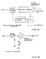
- An ultrasonically oscillating magnetic field may be generated from a base station by a resonant coil or set of coils.
- the transponder may contain a tuned pickup coil which may extract power and timing and/or other information from the magnetic field.
- the frequency, magnitude and/or phase of the magnetic field generated by the coil(s) may be carefully controlled to enable the power picked up by the transponder coil to be adequate for most transponder orientations.
- Identification codes and/or specially stored or other information may be transmitted from the transponder to a receiver, conventionally, by an RF or other suitable signal, depending upon the application of the transponder.
- Programming and/or interrogation of temporary or permanent memory on a selected transponder may be performed conventionally, for example, by modulation of the powering field.
- Frequency shift keying (FSK) is the preferred modulation method.
- each transponder may generate one or more carrier frequencies from an available set of carrier frequencies. These carrier frequencies may not be harmonically related to the frequency of the powering magnetic field.
- a number of transponders may be identified simultaneously under conditions where co-interference would normally preclude correct identification.
- the number of transmission carrier frequencies and/or transmission breaks (herein referred to as idle states) may be contingent upon the particular application.
- the particular mix of carrier frequencies and/or idle states may be chosen randomly. Inclusion of redundant frequency channels may guard against the possibility of chance external interference of a transponder transmission.
- Each transponder may sequentially transmit an identifying code at a (randomly) selected frequency, selected from the band of available frequencies.
- the identifying code may be used to modulate the selected frequency. Any suitable modulation may be used.
- a transponder may be used to identify objects, such as personnel, livestock, baggage, packages, manufactured goods, stock cargo, stolen goods, vehicles, trains, wagons, shipping containers and security cards, and many other things. Furthermore, it may be incorporated into systems requiring its internal identifying capabilities. For example, inventory control, token cards, debit cards, smart cards and computer security.
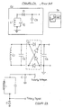
- FIG. 2A shows two prior art arrangements used for receiving power and transmitting an identifying code.
- the receiving portion (RX) receives an inductive powering field.
- the RX arrangement stores a voltage in the storage capacitor (CS), which voltage is used by other circuits on the prior art transponder.
- the rectifying structure (D) being position inter-adjacent the receiving coil and the storage capacitor serves only as a unidirectional regulator and does not allow current to flow from the storage capacitor, through the coil, to ground.
- the transmitter portion (TX) continuously transmits an identifying code at a predetermined frequency.
- a plurality of prior art transponders when simultaneously powered, all transmit simultaneously at the same, set, predetermined frequency.
- the prior art does not lend itself to multiple transponder operation. Furthermore, the prior art does not include an interrogable and/or re-writeable transponder information, data or signal storage. More importantly, the prior art is not adapted to receive power and transmit data from a coil, simultaneously.
- FIG. 2B shows a power and/or data receiving portion of the present invention.
- An externally applied inductive powering field may be applied to the coil (L).
- the field may be modulated with timing, data or other information to be used by the transponder.
- the coil may extract power and timing or data information, if any, from the applied field.
- One or more diodes may be used to rectify the voltage induced to the coil by the applied field. The addition of more complicated rectifying structures may not be necessary as they may not improve the dc conversion efficiency. The voltage drop across more than one diode may represent excess energy dissipation.
- the rectified voltage may be stored in the storage means (C). The stored voltage may be used to supply a dc voltage to transponder internal circuitry.
- diode(s) or any other demodulation means may be used to provide the timing and/or data information (shown as timing signal) for use by the transponder.
- the diode(s) may also interact with the charge storage means to set the supply voltage for the transponder.
- FIG. 2C A modified form of Figure 2B is shown in Figure 2C.
- load loss must be substantially equal to the tuned circuit loss(es). Under these conditions, the output voltage will approach a maximum value.
- the embodiment as shown in Figure 2C may provide load matching, by tapping the pickup coil at an appropriate point. In this way, the coil may act like an autotransformer.
- FIG. 3A shows a basic embodiment of the present invention.
- the inductive means may be divided into an upper (first) portion and a lower (second) portion.
- An impinging inductive powering field (P) may influence the inductive means (as a whole) to provide power (or a voltage) at point V.
- the power V may be used to drive or operate a driver means.
- the driver means may be coupled at the junction of the first and second portions of the inductive means. When the driver means is powered, it may control the first portion of the inductive means in a manner that makes the first portion radiate a signal (S).
- the radiating signal may be produced from the first portion at the same time the powering field is influencing the first and second portions.
- the present invention may provide a means whereby both power reception and signal transmission may be performed simultaneously from at least a portion of the means.
- the inductive means may include only a first portion. In this case, the whole inductive means would operate to simultaneously receive power and transmit signal information.
- Figure 3B shows another embodiment of the present invention.
- the inductive means may provide a signal.
- Rectifier means (D) or a diode may rectify the received signal and provide a voltage for storage in storage means (CS).
- the rectifier means (D) and storage means (CS) may co-operate to form a useable voltage supply for use by other transponder circuitry.
- the rectifier means may rectify the received signal such that the storage means receives a signal burst, which is stored, and outputs a substantially constant voltage for the other transponder circuits until the stored voltage is either depleted or another signal burst replenishes the voltage stored in the storage means whereby the substantially constant voltage is continued to be provided.
- the rectifier means may also provide a clamping means for maintaining the output of the storage means at a substantially constant level, as long as the storage means has a useable charge stored therein.
- an appropriate signal may be applied to the point indicated as output driver. This may cause a conduction path to be selectively formed through all or part of the inductive means (the transmitting section). Because the rectifying means is placed between a point of reference potential and the inductive means, the inductive means is substantially isolated (in a signal sense) from the reference potential. Therefore, when the conduction path is formed, current flows from the voltage supply or another source other than the reference potential, through the inductive means (all or part thereof), thereby causing a signal to be radiated from the inductive means. In this way, a modulated radio frequency (RF) signal or another type of signal may be injected into the transmitting part of the inductive means.
- RF radio frequency
- a feature of the present invention is that a single antenna can be used for simultaneous powering, data reception and data transmission. These three operations occur independently of each other in the same antenna coil.
- Power is supplied by induction which induces a voltage and current in the antenna coil.
- Received data is transmitted by frequency modulating the powering induction signal. Frequency modulation of the induction field does not effect the power received by the transponder's antenna coil.
- Isolation of the data transmission signal is achieved by injecting the transmission signal using a high impedance source (i.e. current source). Current injection does not affect the voltages induced by the powering field or the reception of the Rx data.
- the simplest practically integratable current source is a transistor operated in its current limiting region (i.e. linear region for a bipolar, and saturation region for a FET).
- the collector of a bipolar, or drain of a FET transistor, respectively function as current sources.
- the maintenance of current source action necessitates that the voltage across the transistor is always greater than the saturation voltage. This is typically 0.2 volts for bipolar transistor and roughly 1.0 volt for a FET.
- Figure 11 shows a basic circuit schematic which includes a current source output driver and rectifier to generate DC potential off the antenna coil.
- Figure 12 shows a prior art basic schematic.
- point "B" in Figure 12 is chosen as the reference potential in transponder systems. By choosing “B” as the reference, the potential between B and any part of the antenna coil will swing above and below the reference potential during each cycle of the powering field. A transistor current source connected between the reference point and a tap off the coil will not work during the negative excursions of voltage.
- “A” in Figure 11 as the reference potential between "A” and any point on the antenna coil will not change sign (be it negative or positive) for an ideal rectifier. Even where there is a small voltage drop across the rectifier a tap off the antenna coil will not have a sign change and is an ideal point to connect a transistor current source.
- FIG 13 shows a circuit optimised for an NMOS process. If PMOS is used, the potentials of all points are simply reversed. The critical point is that the rectifier and the current source must share the same potential point, with the other side of the rectifier connected to the end of the inductive antenna furtherest away from the other circuit potential point, and the other side of the current source connected to a tap off the inductive means.
- the circuit shown in Figure 11 can be turned upside down without changing its operation and the DC reference potential point chosen as B. Any form of unidirectional current flow control will work in the circuit, however a synchronous rectifier as detailed in copending Australian Patent Application Provisional Specification No. PI 5507, entitled “Integratable Synchronous Rectifier” filed 19th November, 1987, provides superior performance to a conventional diode.
- FIG. 14 shows a current mirror (a commonly integrated structure) capable of delivering several currents of arbitrary frequency and waveform to the antenna coil.
- the currents I1, I2,...In are linearily summed by the current mirror which outputs Iout. This allows two or more data signals at different frequencies to be simultaneously transmitted.
- the signals can have any arbitrary frequency and waveshape and still be transmitted independently by the antenna coil.
- Figure 15 shows a simple circuit where the current from several output transistors are summed into the antenna coil.
- the inductive means may comprise a coil preferably wire wound, the transmitting part thereof may therefore comprise all of the coil or only a few turns of wire.
- An antenna structure wiring an aluminium laminated plastic film as detailed in Australian Patent Application Provisional Specification No. PI 5855 (entitled “Antenna Structure, Power and Communication System and Methods", filed 10th December, 1987) is advantageously used here.
- the rectifier means may be used to rectify the voltage induced in the transponder pickup coil.
- Storage means preferably a capacitor of an appropriate size and value, may be used to store the rectified voltage. Regulation of the voltage may be enhanced by ensuring that the transponder only moves through those regions of the inductive powering field which will give a tolerated and/or correct voltage.
- the transponder may otherwise include a predetermined voltage cut-off means, the cut-off voltage being an induced voltage below which the transponder will not operate.
- a Zener diode in place of diode (D) in conjunction with the storage means may be used, and if rated at twice the required supply voltage, for example, will rectify the picked-up induced voltage and clamp the supply rail voltage to about one half the diode breakdown voltage until the transponder is no longer under the influence of the powering field.
- a shunt regulator placed across the antenna coil will effectively limit the DC voltage.
- a shunt regulator across the DC supply will limit the DC voltage, however a regulator on the DC line will,
- Shunt regulation is chosen in preference to series regulation because:
- the driver means (T) operated by a driver signal may be a transistor or FET or any other appropriate driver means which may affect transmission through the coil.
- a tuning means (CT) may be used to tune the inductive means.
- the tuning means may include a capacitor.
- the tuning means may enhance the amplitude of signal(s) received and/or transmitted using the induditive means.
- the inductive means is preferably tuned to the received signal.
- the tuning means electrically connects both ends of the coil together at RF frequencies, and hence to the reference potential through the storage capacitor. In effect the tuning and storage capacitors decouple both ends of the coil to the reference potential. Consequently the impedance of the rectifier has no effect upon the action of the RF currents injected into the coil.
- Figures 3C and 3D show alternative embodiments of the present invention.
- coils A, B and C may receive an applied powering field and coil A (and B if D conducts) may simultaneously transmit a signal (including dc and/or ac) when driver T causes a current to be drawn through A (and B when D conducts) and T to a reference rail.
- coils A and B may simultaneously operate as receiver means and transmitter means.
- the transmitter means may be adapted to simultaneously operate as a receiver means.
- Separate coils, one for transmission, another for reception, may also be used in a transponder according to the present invention.
- Figures 4, 4A, 5A, 5B, 6A and 6B, in general, show still further embodiment(s) of the present invention.
- Figures 4 and 4A show two embodiments in a transponder.
- Figure 4A incorporates all circuitry onto the chip except the inductive means. Chip stray capacitance is utilized for charge storage, an external storage capacitor can be utilized if necessary.
- Figures 5A and 5B show an embodiment similar to Figures 4 and 4A but, wherein a coded information signal may be transmitted to a base station from the transponder via the coil, the code so transmitted being stored in the code generator logic.
- Figures 6A and 6B show an embodiment similar to Figures 5A and 5B but, wherein a 'MAG MOD.' signal, which may be superimposed on the power field received by the transponder, provides a means for an interrogating base station to alter, erase or add to information housed within the transponder or otherwise control the transponder, while the transponder is in situ.
- a 'MAG MOD.' signal which may be superimposed on the power field received by the transponder, provides a means for an interrogating base station to alter, erase or add to information housed within the transponder or otherwise control the transponder, while the transponder is in situ.
- any of the component parts may be implemented in a discrete component, hybrid or integrated form, or combination thereof, as may be common in the relevant arts or as required for each particular use of the present invention. Integration of electronic circuitry into chip form may provide an extremely cheap and compact form of transponder.
- An integrated capacitor (Z-folded capacitor and antenna circuit assembly detailed in a copending patent application) may be used as storage means (CS) and coil means, having mounted thereon, the transponder (IC) chip and a coil means. This combination may form a cheap, portable and/or disposable transponder.
- Each transponder may have one or more antenna coils. All, or part of, any or each coil(s) may simultaneously be used to receive and transmit signals. Further description herein is made with reference to a single coiled inductive means in which only part of the inductive means is used to simultaneously transmit and receive signals for the transponder to minimise repetitive detailing.
- the antenna coil may also be used to simultaneously transmit data.
- the transponder design may allow for easy integration of almost all of the electrical circuitry of the transponder.
- the transponder may further include rectifying means (D), which may be in the form of a diode, for rectifying received power.
- the preferred rectifier is a synchronous rectifier as disclosed in copending Australian Provisional Application No. PI 5507, entitled “Integratable Synchronous Rectifier", filed 19th November, 1987.
- the rectifier disclosed therein is readily integratable into the transponder's IC.
- the addition of more complicated rectifying structures such as bridge rectifiers may be unnecessary, since they may not substantially improve the dc conversion efficiency.
- the purpose of D is to rectify the AC signal received by the tuned antenna coil.
- the rectifying structure is positioned unconventionally within the transponder circuit and may allow for easier integration using standard commercial integration techniques and may allow the antenna coil to be further used as an RF or other signal radiator.
- a stable master time reference source typically a crystal controlled oscillator.
- This time reference source is used to operate the frequency of the powering field.
- the transponder's carrier oscillator is phase coherently locked to the master time reference in the interrogator through the interrogator's powering field.
- Phase coherent locking of the signal carrier to the master time reference provides substantial advantages over non-coherent carrier generation.
- the carrier signal can be coherently detected at the interrogator using well understood coherent detection principles with the master time reference serving as the frequency reference for the coherent detection circuits.
- Coherent detection provides optimum signal to noise detection, excellent interference suppression and sideband rejection.
- Figure 1 shows this time reference signal being fed to the "receiver and decoder" circuitry in the interrogator.
- the time reference signal is used by the "frequency and phase” controller to generate the frequency of the powering field.
- a storage capacitor a preferred form of storage means (CS) may be used to store the dc electrical power periodically supplied by the tuned circuit and diode D. CS stores this pulsed electrical power and may deliver a substantially constant DC voltage to the transponder circuitry via the supply rail.
- a driver means (T) which may be part of the modulator means, and may preferably comprise a MOS transistor incorporated into the transponder circuitry.
- a modulating signal may be drivingly coupled to the gate of T.
- the drain of T may be coupled to the pickup coil and may be adapted to draw a current through all (or part of, depending upon the configuration) of the pickup coil. The current may induce an RF magnetic field in the coil which may radiate a signal or code modulated signal to receiving structure(s) adapted to receive this signal.
- the timing reference point (TR) may provide an appropriate point for obtaining the period of the powering field or other signal information from the powering field which may be used as a timing reference for any of the transponder circuitry, preferably the carrier ocsillator(s).
- the carrier oscillator(s) may, however, be preset and therefore the timing reference may have other applications within the transponder, for example, enabling means or data means, programming electrically erasable memory (such as EEPROM) where the peak reference potential (twice the supply voltage) could be required for memory programming.
- the (tuned) coil circuit may be tuned to the power frequency, rather than the RF frequency.
- RF current may be drawn through the top turns of the tap from the supply capacitance (CS) during transponder transmission. Only one coil (with a tap) may be necessary.
- a tuning capacitance (CT) may be coupled to the pickup coil structure to which the DC storage capacitance (CS) may also be coupled.
- the rectifier is conveniently shown as a diode D the preferred integratable form is a synchronous rectifier.
- FIG. 4 shows an illustration of the relationship between the inductive pickup (coil), tuning capacitor (CT), storage capacitor (CS), rectifier (D), timing reference (TR), transistor (T), supply rail (+) and some transponder circuitry.
- the transponder preferably incorporates an integrated circuit (IC) which includes any necessary electronic functions.
- the IC may monitor the voltage induced in the pickup coil at the time reference point TR.
- the carrier oscillator may be a phase locked high frequency oscillator, the output of which may be used as a data carrier for transmitting information. Simple multiplication of the power frequency by the oscillator may not be advantageous because harmonics generated by the power field will interfere with the oscillator's signal carrier.
- FIGs 7A to 7H show preferred schematic embodiments of portions of the transponder as shown before in functional block form.
- the 'MAG MOD' signal shown in Figure 7B (and Figure 6) is the magnetic modulation signal. This modulation may be superimposed on the powering field.
- the preferred form of magnetic modulation is frequency shift keying (FSK).
- FSK'ing the magnetic field does not alter the power received by the antenna coil. When the antenna coil is tuned there is a slight frequency dependent reduction in power conversion. This is very small for low deviation FSK and low Q tuning of the antenna coil.
- FSK signalling with the power field is particularly useful providing simultaneous power transmission to, and data reception by, the transponder antenna completely independent of each function.
- the signal may provide a basis for control of the transponder and/or, more specifically, enable control of preset data or other signals and/or to initiate programming or other functions of circuits in the transponder.
- Embodiments of carrier oscillator are shown in Figures 7A and 7B.
- Embodiments as shown in Figures 7G and 7H may also be used in the transponder, and may provide an ability to randomly select a carrier frequency from a set of available carrier frequencies. This random selection may aid in transponder/base station communication when the transponder is used in a multiple transponder system.
- the output of the carrier oscillator may be divided down to provide a logic clock signal (also shown in Figures 5A, 5B and 6A, 6B). A divided output may provide a logic signal even when the timing reference is momentarily unavailable.
- the carrier oscillator may be designed to remain substantially stable during short interruptions to the timing reference signal..
- the timing reference may be divided down and used directly as a clock signal.
- the logic clock may be used to derive a preset, pre-programmed, alterable or selectable code from a set of logic gates or memory. This code may be used to modulate the carrier signal. Phase modulation is a preferred implemented modulation technique.
- a simple EXCLUSIVE OR gate ( Figure 7F) may be used to phase modulate the carrier, however, amplitude, pulse position, pulse width or any other modulation may be possible.
- the modulated carrier signal may be used to drive the gate of T, which may operate in its saturated region i.e.: like a current source, and may draw a fixed magnitude current at the carrier frequency. This current may generate a magnetic field oscillating at the carrier frequency which will radiate from the transponder.
- a current mirror drive can drive the output transistor and the mirror current can be modulated to deliver envelope shaped bandwidth limited RF data to the antenna.
- Envelope shaping of RF modulated data provides good sideband suppression and normally necessitates the use of complex filters to generate it.
- the current mirror readily lends itself to waveshape synthesis.
- Figure 16A shows a basic schematic of an integratable circuit for waveshape synthesis
- 16B shows a more detailed circuit capable of synthesising a band limited data signal. The use of current summing either through current mirrors and/or through parallel output transistors allows
- the divider may be connected to a time base input or to the carrier oscillator.
- a transponder when powered may begin to transmit its code or other information. Transmission may be selectably switched. Transmission may also be continuous while the transponder is receiving a power field. The transmission may be based on a preferably randomly selected frequency or frequencies, from a possible set of frequencies or transmission breaks.
- the carrier frequency(s), the output of the oscillator means, may be generated by one or more voltage controlled oscillators (VCO's), each in a phase locked loop configuration controlled by the inductive powering frequency.
- VCO's voltage controlled oscillators
- the output carrier frequency may be substantially equal to (p + n m ) x frequency of inductive power field.
- n is less than m, the carrier frequency may never be equal to a harmonic of the powering frequency. Consequently, the powering field's harmonics may never interfere with the carrier transmissions.
- the carrier frequency may be set.
- Various carrier frequencies may be generated by either using one oscillator and adjusting n as required or having many selectable oscillator(s) each with a different preset n generating one of the required carrier frequencies.
- Control of the selection of a carrier frequency(s) and/or transmission break(s) may be accomplished with varying degrees of complexity by implementation of the selection circuitry.
- a pulse of modulation (MAG MOD) on the powering field, may cause a transponder to randomly select a carrier frequency or transmission break.
- MAG MOD pulse of modulation
- suitable detection and decoding circuitry on the transponder By appropriate coding of the modulation of the powering field, coupled with suitable detection and decoding circuitry on the transponder, more elaborate selection schemes or communication methods may be implemented. For example, a transponder may be forced off air or the carrier frequency of a particular transponder may be changed. Frequency, phase, amplitude or pulse modulation or any combination of these may be used to modulate the inductive powering field.
- a transponder may randomly select either a transmission break or carrier frequency. Arbitrary probability weightings may also be assigned to each carrier frequency and/or idle state. Selection may be made following the transmission of a complete code or data word. In this manner, the carrier frequency of the transponder may be altered after each completed code or data word transmission. Also, the transmission of more than one code or data word before reselecting the carrier frequency may be possible.
- the modulator shown in the various Figures may comprise an EXCLUSIVE-OR gate. If so, the RF output consists of Binary Phase Shift Keyed data (BPSK). Other more complicated modulator embodiments may require Quadrature Phase Shift Keying (QPSK). AM or FM modulators may also be used.
- BPSK Binary Phase Shift Keyed data
- QPSK Quadrature Phase Shift Keying
- AM or FM modulators may also be used.
- a one, two or three dimensional antenna base structure may be used to radiate the powering field for the transponder.
- the modulation rate may be limited by the bandwidth of the transponder. This may be sufficiently large to allow a data rate of any required number of kilobits per second.
- the magnetic field may be phase or frequency modulated as these may not affect the power transmission from the base station to the transponder. Amplitude, pulse width or pulse position modulation may also be used.
- a phase locked loop may extract the phase or frequency modulation, while a simple envelope detector or other means may be used to detect amplitude or pulse modulation.
- the oscillating magnetic field may be generated by an oscillator with a tuned coil. Tuning may be essential for supplying large coil currents at low input voltages. A high Q coil may be used for more efficient operation. The intrinsic properties of a high Q tuned coil require special attention if high speed modulation of the magnetic field is required.
- the instantaneous operating frequency of the tuned coil may be changed by either a step change in the coil inductance or tuning capacitance. Any step inductance change may preferably occur when the coil current is zero while any step capacitance change may preferably occur when the capacitor voltage is zero. Examples of switching schemes, to alleviate any circuit transient responses are shown in Figures 9A and 9B.
- phase modulation the phase angle may slip at a linear rate when a step frequency change is made. When the required phase angle slippage is reached, the operating frequency is returned to its nominal value and the phase slippage ceases.
- the coil Q may mitigate against rapid changes in the coil current.
- the coil Q may be artifically lowered by inserting extra loss in to the coil. This may be done by either directly, inductively or capacitively introducing extra resistance in to the tuned circuit.
- reductions in the coil current magnitude may be sped up by switching in an extra resistor.
- the resistor may be connected after the signal source has been disconnected. The resistor may rapidly quench the coil current. After the appropriate time interval has elapsed the signal source may be re-activated and the coil current may be re-established.
- the resistance may be replaced by the power supply so that instead of dumping the magnetic energy as heat it may be returned for reuse by the power supply.
- the simultaneous action of power transfer and data or command transmission by the same magnetic field may allow the remote control of electromechanical devices and electronic circuits, for example, the remote programming of EEPROM or conventional CMOS memory in a known manner.
- Figures 17 and 18 refer to an embodiment of the present invention in which all of the transponder circuitry including the antenna are incorporated onto a single chip.
- Such an embodiment is ideally suited to smart card applications eg credit, debit and token cards where the chip to interrogator coupling can be arranged to be strong enough to power the chip from such a small antenna. Strong coupling ensures that there is sufficient voltage without tuning.
- Tuning magnifies the voltage induced in the antenna coil by the "Q" of the tuned circuit, typically 5 for this type of antenna.
- the storage capacitor is realized using the stray capacity of the chip ie leads, pads, metalisation and by making capacitors on any spare chip area.
- the present invention remarkably provides a device adapted for simultaneous power reception, data reception and signal transmission from a single inductive means.
- the present invention is substantially entirely adapted for integration.
- the present invention provides a unique circuit combination and/or configuration.
- the present invention is particularly adapted for use in a transponder, however, the general applicability of the present invention should not be limited to a transponder.
Landscapes
- Engineering & Computer Science (AREA)
- General Physics & Mathematics (AREA)
- Physics & Mathematics (AREA)
- Theoretical Computer Science (AREA)
- Computer Networks & Wireless Communication (AREA)
- Microelectronics & Electronic Packaging (AREA)
- Computer Hardware Design (AREA)
- Artificial Intelligence (AREA)
- Computer Vision & Pattern Recognition (AREA)
- Signal Processing (AREA)
- Radar Systems Or Details Thereof (AREA)
- Near-Field Transmission Systems (AREA)
- Investigating Or Analyzing Materials By The Use Of Ultrasonic Waves (AREA)
Claims (14)
- Dispositif de réception d'un champ d'alimentation inducteur et de rayonnement d'un signal d'information, le dispositif comprenant :
des moyens d'entraînement (T) pour contrôler le rayonnement du signal d'information par le dispositif ;
des moyens inducteurs (L) pour recevoir le champ d'alimentation inducteur pour fournir de la puissance aux moyens d'entraînement ; et
des moyens de rectification (D) couplés à un côté des moyens inducteurs ;
caractérisé en ce que les moyens de rectification sont couplés entre ledit premier côté des moyens inducteurs et un point de potentiel de référence pour le dispositif dans son ensemble, et en ce que les moyens d'entraînement comprennent une source de courant couplée aux moyens inducteurs pour permettre à au moins une partie des moyens inducteurs de simultanément recevoir le champ d'alimentation et rayonner le signal d'information sans interaction entre eux. - Dispositif selon la revendication 1, dans lequel les moyens de rectification (D) sont couplés de manière à coopérer avec les moyens inducteurs (L) pour délivrer une tension d'alimentation de l'autre côté des moyens inducteurs lorsque le champ d'alimentation est reçu.
- Dispositif selon la revendication 2, dans lequel les moyens d'entraînement (T) sont couplés entre le point de potentiel de référence et une prise des moyens inducteurs (L).
- Dispositif selon la revendication 3, dans lequel la source de courant est couplée aux moyens inducteurs (L) pour provoquer sélectivement l'écoulement d'un courant dans les moyens inducteurs entre la prise et ledit autre côté des moyens inducteurs pour rayonner le signal d'information.
- Dispositif selon la revendication 4, dans lequel le courant est un courant à modulation de code.
- Dispositif selon l'une quelconque des revendications précédentes, dans lequel les moyens d'entraînement (T) comprennent des miroirs de courant ou des transistors à sorties parallèles, l'un de ceux-ci effectuant une sommation en courant.
- Dispositif selon l'une quelconque des revendications précédentes, caractérisé en ce- que les moyens inducteurs (L) sont une bobine inductrice simple.
- Dispositif selon l'une quelconque des revendications précédentes, dans lequel le signal d'information est un signal de radiofréquence.
- Dispositif selon l'une quelconque des revendications précédentes, dans lequel les moyens inducteurs (L) sont agencés pour recevoir un signal de données simultanément au champ d'alimentation inducteur.
- Dispositif selon la revendication 9, dans lequel le signal de données est de la forme d'une modulation par déplacement de fréquence du champ d'alimentation.
- Dispositif selon l'une quelconque des revendications précédentes, comprenant des moyens de stockage de charge (CS) pour stocker la puissance délivrée par les moyens inducteurs (L).
- Dispositif selon l'une quelconque des revendications précédentes, dans lequel les moyens inducteurs (T) et les moyens de rectification (D) sont réalisés dans une seule puce intégrée.
- Dispositif selon la revendication 1, le dispositif étant prévu dans une seule puce intégrée.
- Dispositif selon la revendication 12 ou 13, le dispositif étant incorporé dans une carte intelligente ou un marquage d'identification.
Applications Claiming Priority (3)
| Application Number | Priority Date | Filing Date | Title |
|---|---|---|---|
| AUPI547987 | 1987-11-18 | ||
| AU5479/87 | 1987-11-18 | ||
| PCT/AU1988/000449 WO1989005067A1 (fr) | 1987-11-18 | 1988-11-18 | Repondeur |
Publications (3)
| Publication Number | Publication Date |
|---|---|
| EP0393089A1 EP0393089A1 (fr) | 1990-10-24 |
| EP0393089A4 EP0393089A4 (en) | 1991-09-11 |
| EP0393089B1 true EP0393089B1 (fr) | 1995-07-05 |
Family
ID=3772585
Family Applications (1)
| Application Number | Title | Priority Date | Filing Date |
|---|---|---|---|
| EP88909960A Expired - Lifetime EP0393089B1 (fr) | 1987-11-18 | 1988-11-18 | Repondeur |
Country Status (9)
| Country | Link |
|---|---|
| US (1) | US5153583A (fr) |
| EP (1) | EP0393089B1 (fr) |
| JP (1) | JPH03502032A (fr) |
| AT (1) | ATE124829T1 (fr) |
| AU (1) | AU2781089A (fr) |
| CA (1) | CA1326889C (fr) |
| DE (1) | DE3854129T2 (fr) |
| WO (1) | WO1989005067A1 (fr) |
| ZA (1) | ZA888681B (fr) |
Cited By (2)
| Publication number | Priority date | Publication date | Assignee | Title |
|---|---|---|---|---|
| US7495276B2 (en) | 2004-02-05 | 2009-02-24 | Infineon Technologies Ag | Radio frequency arrangement, method for producing a radio frequency arrangement and use of the radio frequency arrangement |
| US8115635B2 (en) | 2005-02-08 | 2012-02-14 | Abbott Diabetes Care Inc. | RF tag on test strips, test strip vials and boxes |
Families Citing this family (130)
| Publication number | Priority date | Publication date | Assignee | Title |
|---|---|---|---|---|
| ZA892468B (en) * | 1988-04-11 | 1989-12-27 | Uniscan Ltd | Improvements in or relating to cutting elements foactuator and communication system r rotary drill bits |
| US5701121A (en) * | 1988-04-11 | 1997-12-23 | Uniscan Ltd. | Transducer and interrogator device |
| JP2908014B2 (ja) * | 1989-02-17 | 1999-06-21 | インテグレーテッド・シリコン・デザイン・ピーティーワイ・リミテッド | トランスポンダ・システム |
| AU665929B2 (en) * | 1989-05-26 | 1996-01-25 | Trovan Limited | Method and apparatus for modulating and dectecting a subcarrier signal for an inductively coupled transponder |
| US5327122A (en) * | 1989-09-04 | 1994-07-05 | Massimo Casalegno | Installation for data transmission with correction of phase error |
| DE4003410A1 (de) * | 1990-02-05 | 1991-08-08 | Anatoli Stobbe | Tragbares feldprogrammierbares detektierplaettchen |
| AT395224B (de) * | 1990-08-23 | 1992-10-27 | Mikron Ges Fuer Integrierte Mi | Kontaktloses, induktives datenuebertragungssystem |
| DE4034225C2 (de) * | 1990-10-26 | 1994-01-27 | Reinhard Jurisch | Datenträger für Identifikationssysteme |
| CA2074702C (fr) * | 1991-07-29 | 1996-11-19 | Donald J. Urbas | Transpondeur programmable |
| GB9202831D0 (en) | 1992-02-11 | 1992-03-25 | Shanning Laser Systems Ltd | Security tag |
| JP3216205B2 (ja) * | 1992-03-27 | 2001-10-09 | 神鋼電機株式会社 | 半導体製造システムにおけるid認識装置 |
| ZA935944B (en) * | 1992-08-14 | 1994-03-10 | Megellan Corp Australia Pty Lt | Identification apparatus |
| ATE201787T1 (de) * | 1992-11-25 | 2001-06-15 | Simmonds Precision Products | Datenverarbeitungsstrukturen und methoden |
| US5423334A (en) * | 1993-02-01 | 1995-06-13 | C. R. Bard, Inc. | Implantable medical device characterization system |
| US5581248A (en) * | 1993-06-14 | 1996-12-03 | Simmonds Precision Products, Inc. | Embeddable device for contactless interrogation of sensors for smart structures |
| US5433115A (en) * | 1993-06-14 | 1995-07-18 | Simmonds Precision Products, Inc. | Contactless interrogation of sensors for smart structures |
| US5602540A (en) * | 1993-06-14 | 1997-02-11 | Simmonds Precision Products Inc. | Fluid gauging apparatus with inductive interrogation |
| US5515041A (en) * | 1993-06-14 | 1996-05-07 | Simmonds Precision Products Inc. | Composite shaft monitoring system |
| US5382780A (en) * | 1993-10-01 | 1995-01-17 | Duncan Industries Parking Control Systems Corp. | Portable time metering device |
| DE4417688C1 (de) * | 1994-05-20 | 1995-07-13 | Licentia Gmbh | Beweglicher Gegenstand mit einem Transponder |
| US6472975B1 (en) * | 1994-06-20 | 2002-10-29 | Avid Marketing, Inc. | Electronic identification system with improved sensitivity |
| GB9416349D0 (en) * | 1994-08-12 | 1994-10-05 | Neopost Ltd | Mailing system |
| US6249212B1 (en) * | 1994-10-05 | 2001-06-19 | Avid Marketing, Inc. | Universal electronic identification tag |
| JPH0962816A (ja) * | 1994-10-06 | 1997-03-07 | Mitsubishi Electric Corp | 非接触icカードおよびこれを含む非接触icカードシステム |
| US5626630A (en) * | 1994-10-13 | 1997-05-06 | Ael Industries, Inc. | Medical telemetry system using an implanted passive transponder |
| US5767792A (en) * | 1994-10-13 | 1998-06-16 | Bio Medic Data Systems Inc. | Method for calibrating a temperature sensing transponder |
| US5510795A (en) * | 1994-11-10 | 1996-04-23 | Amtech Corporation | Single antenna location and direction finding system |
| US5648765A (en) * | 1995-03-08 | 1997-07-15 | Cresap; Michael S. | Tag tansponder system and method to identify items for purposes such as locating, identifying, counting, inventorying, or the like |
| US6329139B1 (en) | 1995-04-25 | 2001-12-11 | Discovery Partners International | Automated sorting system for matrices with memory |
| US5838253A (en) * | 1995-05-17 | 1998-11-17 | Accu-Sort Systems, Inc. | Radio frequency identification label |
| US7511621B1 (en) | 1995-08-31 | 2009-03-31 | Intermec Ip Corp. | High-performance mobile power antennas |
| US5859419A (en) * | 1995-09-28 | 1999-01-12 | Sol H. Wynn | Programmable multiple company credit card system |
| JP3378435B2 (ja) * | 1995-09-29 | 2003-02-17 | 株式会社東芝 | 超高周波帯無線通信装置 |
| US5736332A (en) * | 1995-11-30 | 1998-04-07 | Mandecki; Wlodek | Method of determining the sequence of nucleic acids employing solid-phase particles carrying transponders |
| US5641634A (en) | 1995-11-30 | 1997-06-24 | Mandecki; Wlodek | Electronically-indexed solid-phase assay for biomolecules |
| US6001571A (en) * | 1995-11-30 | 1999-12-14 | Mandecki; Wlodek | Multiplex assay for nucleic acids employing transponders |
| US6051377A (en) * | 1995-11-30 | 2000-04-18 | Pharmaseq, Inc. | Multiplex assay for nucleic acids employing transponders |
| WO1997019958A1 (fr) | 1995-11-30 | 1997-06-05 | Wlodek Mandecki | Criblage des drogues a partir de bibliotheques chimiques combinatoires au moyen de transpondeurs |
| FR2743649B1 (fr) * | 1996-01-17 | 1998-04-03 | Gemplus Card Int | Module electronique sans contact, carte etiquette electronique l'incorporant, et leurs procedes de fabrication |
| US5796180A (en) * | 1996-01-23 | 1998-08-18 | Siemens Aktiengesellschaft | Device for transmitting data or energy |
| US6097292A (en) * | 1997-04-01 | 2000-08-01 | Cubic Corporation | Contactless proximity automated data collection system and method |
| US6941124B1 (en) | 1996-05-13 | 2005-09-06 | Micron Technology, Inc. | Method of speeding power-up of an amplifier, and amplifier |
| US6836468B1 (en) | 1996-05-13 | 2004-12-28 | Micron Technology, Inc. | Radio frequency data communications device |
| US6130602A (en) | 1996-05-13 | 2000-10-10 | Micron Technology, Inc. | Radio frequency data communications device |
| US6774685B2 (en) | 1996-05-13 | 2004-08-10 | Micron Technology, Inc. | Radio frequency data communications device |
| US6696879B1 (en) | 1996-05-13 | 2004-02-24 | Micron Technology, Inc. | Radio frequency data communications device |
| US6058374A (en) * | 1996-06-20 | 2000-05-02 | Northrop Grumman Corporation | Inventorying method and system for monitoring items using tags |
| US5774876A (en) * | 1996-06-26 | 1998-06-30 | Par Government Systems Corporation | Managing assets with active electronic tags |
| US5815020A (en) * | 1996-09-24 | 1998-09-29 | Motorola, Inc. | Balance differential receiver |
| US5812942A (en) * | 1996-09-24 | 1998-09-22 | Motorola, Inc. | Balanced differential radio receiver and method of operation |
| US6118367A (en) * | 1996-11-29 | 2000-09-12 | Yoshikawa Rf Systems Co., Ltd. | Data carrier system |
| JPH10193849A (ja) * | 1996-12-27 | 1998-07-28 | Rohm Co Ltd | 回路チップ搭載カードおよび回路チップモジュール |
| US6208235B1 (en) * | 1997-03-24 | 2001-03-27 | Checkpoint Systems, Inc. | Apparatus for magnetically decoupling an RFID tag |
| US5981166A (en) * | 1997-04-23 | 1999-11-09 | Pharmaseq, Inc. | Screening of soluble chemical compounds for their pharmacological properties utilizing transponders |
| JPH1111055A (ja) * | 1997-06-20 | 1999-01-19 | Toshiba Corp | 無線モジュール及び無線カード |
| US5880945A (en) * | 1997-06-30 | 1999-03-09 | Intel Corporation | Power conversion and load circuit on same integrated circuit |
| US6177859B1 (en) * | 1997-10-21 | 2001-01-23 | Micron Technology, Inc. | Radio frequency communication apparatus and methods of forming a radio frequency communication apparatus |
| FR2778521B1 (fr) * | 1998-05-06 | 2000-06-16 | Sgs Thomson Microelectronics | Circuit codeur bpsk |
| US6154137A (en) * | 1998-06-08 | 2000-11-28 | 3M Innovative Properties Company | Identification tag with enhanced security |
| US8228193B1 (en) * | 1998-09-14 | 2012-07-24 | Tuemer Tuemay O | Tag having a semiconductor chip and method of attachment to article |
| DE50001701D1 (de) * | 1999-01-21 | 2003-05-15 | Enocean Gmbh | Anordnung zum erzeugen eines eine information tragenden antwortsignals und verfahren zur fernabfrage einer solchen anordnung |
| US8538801B2 (en) * | 1999-02-19 | 2013-09-17 | Exxonmobile Research & Engineering Company | System and method for processing financial transactions |
| FR2791489B1 (fr) * | 1999-03-25 | 2001-06-08 | Inside Technologies | Procede de modulation de l'amplitude d'un signal d'antenne |
| DE50015873D1 (de) * | 1999-06-11 | 2010-04-08 | Abb Research Ltd | System für eine eine vielzahl von aktoren aufweisende maschine |
| US8648692B2 (en) | 1999-07-23 | 2014-02-11 | Seong Sang Investments Llc | Accessing an automobile with a transponder |
| US6952155B2 (en) * | 1999-07-23 | 2005-10-04 | Himmelstein Richard B | Voice-controlled security system with proximity detector |
| DE19938998B4 (de) * | 1999-08-17 | 2008-01-17 | Infineon Technologies Ag | Verfahren zum Betreiben von Chipkarten |
| US6282231B1 (en) | 1999-12-14 | 2001-08-28 | Sirf Technology, Inc. | Strong signal cancellation to enhance processing of weak spread spectrum signal |
| IT1311298B1 (it) * | 1999-12-31 | 2002-03-12 | Urmet Sud Costruzioni Elettro | Sistema di autotassazione e verifica particolarmente per parcheggi apagamento per autoveicoli. |
| JP3885922B2 (ja) * | 2000-03-07 | 2007-02-28 | 株式会社ルネサステクノロジ | 半導体チップとそれを用いたicカード及びrfid |
| DE10108243A1 (de) * | 2001-02-21 | 2002-08-22 | Abb Research Ltd | System für eine Vielzahl von Sensoren und/oder Aktoren aufweisende Maschine oder Anlage |
| DE20105592U1 (de) * | 2001-03-30 | 2002-05-23 | Siemens AG, 80333 München | Sensoreinrichtung mit einem passiven Bauelement zur Abfrage und Mitteilung eines Systemzustands eines technischen Systems |
| US7003167B2 (en) * | 2001-11-01 | 2006-02-21 | Hewlett-Packard Development Company, L.P. | Single-pass guaranteed-fit data compression using rate feedback |
| DE10201505B4 (de) * | 2002-01-17 | 2004-03-18 | Dbt Automation Gmbh | Arbeitsschutzvorrichtung für Bergleute |
| WO2003063103A1 (fr) | 2002-01-18 | 2003-07-31 | Georgia Tech Research Corporation | Controle et suivi d'actifs par reseau de communication sans fil |
| US6970089B2 (en) | 2002-07-03 | 2005-11-29 | Battelle Memorial Institute K1-53 | Full-spectrum passive communication system and method |
| US6707376B1 (en) * | 2002-08-09 | 2004-03-16 | Sensormatic Electronics Corporation | Pulsed power method for increased read range for a radio frequency identification reader |
| AU2002950973A0 (en) | 2002-08-22 | 2002-09-12 | Magellan Technology Pty Ltd | A radio frequency identification ("rfid") device |
| DE10301451A1 (de) * | 2003-01-10 | 2004-07-22 | Atmel Germany Gmbh | Verfahren sowie Sende- und Empfangseinrichtung zur drahtlosen Datenübertragung und Modulationseinrichtung |
| DE10306689A1 (de) * | 2003-02-11 | 2004-08-19 | Atmel Germany Gmbh | Schaltungsanordnung zur Signaldetektion |
| DE10305833B3 (de) | 2003-02-12 | 2004-08-12 | Siemens Audiologische Technik Gmbh | Datenübertragungseinrichtung für Hörgeräte |
| SE526370C2 (sv) * | 2003-04-14 | 2005-08-30 | Delaval Holding Ab | Digital transponderläsare |
| DE10322888A1 (de) * | 2003-05-21 | 2004-12-16 | Atmel Germany Gmbh | Intergrierter Schaltkreis mit Transponder |
| DE10325396A1 (de) * | 2003-05-28 | 2004-12-23 | Atmel Germany Gmbh | Schaltungsanordnung und Verfahren zur Phasenmodulation für rückstreubasierte Transponder |
| DE10325399A1 (de) * | 2003-05-28 | 2004-12-30 | Atmel Germany Gmbh | Schaltungsanordnung zur Phasenmodulation für rückstreubasierte Transporder |
| US20050012597A1 (en) * | 2003-07-02 | 2005-01-20 | Anderson Peter Traneus | Wireless electromagnetic tracking system using a nonlinear passive transponder |
| US8026729B2 (en) | 2003-09-16 | 2011-09-27 | Cardiomems, Inc. | System and apparatus for in-vivo assessment of relative position of an implant |
| WO2005027998A2 (fr) | 2003-09-16 | 2005-03-31 | Cardiomems, Inc. | Detecteur implantable sans fil |
| DE102004019572A1 (de) * | 2004-04-22 | 2005-11-10 | Hella Kgaa Hueck & Co. | Vorrichtung zum Auslesen von Sensoren im Motorraum eines Kraftfahrzeuges |
| DE102005035346A1 (de) * | 2004-08-19 | 2006-03-09 | Atmel Germany Gmbh | Verlustleistungsoptimierter Hochfrequenz-Koppelkondensator und Gleichrichterschaltung |
| US7649496B1 (en) * | 2004-10-12 | 2010-01-19 | Guy Silver | EM rectifying antenna suitable for use in conjunction with a natural breakdown device |
| DE102004062132A1 (de) * | 2004-12-23 | 2006-07-13 | Atmel Germany Gmbh | Backscatter Transponder |
| US7908080B2 (en) | 2004-12-31 | 2011-03-15 | Google Inc. | Transportation routing |
| US8010048B2 (en) | 2005-01-20 | 2011-08-30 | Bae Systems Information And Electronic Systems Integration Inc. | Microradio design, manufacturing method and applications for the use of microradios |
| US8160497B2 (en) | 2005-01-20 | 2012-04-17 | Bae Systems Information And Electronic Systems Integration Inc. | Method of determining conditions on the ground using microradios |
| US7307530B2 (en) * | 2005-02-10 | 2007-12-11 | Fabian Carl E | Surgical implement detector utilizing a radio-frequency identification marker |
| WO2007002185A2 (fr) | 2005-06-21 | 2007-01-04 | Cardiomems, Inc. | Procede de fabrication de capteur sans fil implantable pour la mesure de pression in vivo |
| NZ540927A (en) * | 2005-06-22 | 2008-03-28 | Traffic Electronics Ltd | Communication system for inductive power transfer system |
| EP1902529B1 (fr) * | 2005-07-08 | 2012-06-13 | CardioMems, Inc. | Boucle de couplage, ensemble de cable et procede destine au positionnement d'une boucle de couplage |
| US20190362725A1 (en) | 2005-08-17 | 2019-11-28 | Tamiras Per Pte. Ltd., Llc | Providing access with a portable device and voice commands |
| FR2890207B1 (fr) † | 2005-08-23 | 2007-11-02 | Inside Contactless Sa | Lecteur a couplage inductif comprenant des moyens d'extraction d'une tension d'alimentation electrique |
| US20070057469A1 (en) * | 2005-09-09 | 2007-03-15 | Shuffle Master, Inc. | Gaming table activity sensing and communication matrix |
| DE102005060914A1 (de) * | 2005-12-20 | 2007-06-28 | Atmel Germany Gmbh | Verfahren zum Übertragen von Informationen und Signalübertragungssystem, insbesondere zur Zugangskontrolle |
| US8447234B2 (en) * | 2006-01-18 | 2013-05-21 | Qualcomm Incorporated | Method and system for powering an electronic device via a wireless link |
| US9130602B2 (en) | 2006-01-18 | 2015-09-08 | Qualcomm Incorporated | Method and apparatus for delivering energy to an electrical or electronic device via a wireless link |
| US20110267235A1 (en) | 2006-01-20 | 2011-11-03 | Bae Systems Information And Electronic Systems Integration Inc. | Method of tracking a vehicle using microradios |
| US8917178B2 (en) * | 2006-06-09 | 2014-12-23 | Dominic M. Kotab | RFID system and method for storing information related to a vehicle or an owner of the vehicle |
| CA2662917C (fr) | 2006-09-08 | 2013-04-16 | Cardiomems, Inc. | Systeme d'acquisition et de gestion de donnees physiologiques destine a un capteur sans fil implante |
| DE102006057645A1 (de) * | 2006-12-05 | 2008-06-26 | Deutsche Post Ag | Sensor-Transponder-Einheit und Verfahren zu ihrem Betreiben |
| US9774086B2 (en) | 2007-03-02 | 2017-09-26 | Qualcomm Incorporated | Wireless power apparatus and methods |
| US8378522B2 (en) * | 2007-03-02 | 2013-02-19 | Qualcomm, Incorporated | Maximizing power yield from wireless power magnetic resonators |
| US9124120B2 (en) | 2007-06-11 | 2015-09-01 | Qualcomm Incorporated | Wireless power system and proximity effects |
| EP2160710A1 (fr) * | 2007-06-25 | 2010-03-10 | Nxp B.V. | Dispositif électronique et procédé pour la transmission sans contact de données |
| US7970357B2 (en) * | 2007-07-30 | 2011-06-28 | Bae Systems Information And Electronic Systems Integration Inc. | Transponder with stabilized oscillator |
| CN101842962B (zh) | 2007-08-09 | 2014-10-08 | 高通股份有限公司 | 增加谐振器的q因数 |
| US8183982B2 (en) * | 2007-08-14 | 2012-05-22 | Infineon Technologies Ag | System including reply signal that at least partially overlaps request |
| CN101828300A (zh) | 2007-09-17 | 2010-09-08 | 高通股份有限公司 | 用于无线能量转移的发射器和接收器 |
| WO2009049281A2 (fr) | 2007-10-11 | 2009-04-16 | Nigel Power, Llc | Transfert de puissance sans fil utilisant des systèmes magnéto-mécaniques |
| US8629576B2 (en) | 2008-03-28 | 2014-01-14 | Qualcomm Incorporated | Tuning and gain control in electro-magnetic power systems |
| US8810371B2 (en) * | 2008-06-12 | 2014-08-19 | Vicinity Pty Ltd | Antenna design and interrogator system |
| US8111042B2 (en) | 2008-08-05 | 2012-02-07 | Broadcom Corporation | Integrated wireless resonant power charging and communication channel |
| JP5215154B2 (ja) * | 2008-12-09 | 2013-06-19 | ルネサスエレクトロニクス株式会社 | 半導体集積回路装置およびそれを用いた非接触/接触電子装置ならびに携帯情報端末 |
| JP2012023299A (ja) * | 2010-07-16 | 2012-02-02 | Equos Research Co Ltd | 共鳴コイル |
| US8482434B2 (en) * | 2010-09-17 | 2013-07-09 | United Technologies Corporation | Wireless sensor for an aircraft propulsion system |
| DE102011050129B4 (de) * | 2011-05-05 | 2026-02-05 | Maxim Integrated Gmbh | Transponder |
| US9601267B2 (en) | 2013-07-03 | 2017-03-21 | Qualcomm Incorporated | Wireless power transmitter with a plurality of magnetic oscillators |
| US9299232B2 (en) * | 2013-12-20 | 2016-03-29 | Checkpoint Systems, Inc. | Security device with dual use transformer |
| EP3192005B1 (fr) | 2014-09-12 | 2020-10-21 | Sato Holdings Kabushiki Kaisha | Système, appareil et procédé rfid à rayon d'action étendu |
| KR102469570B1 (ko) * | 2015-09-08 | 2022-11-22 | 삼성전자주식회사 | 전자 장치 및 그의 동작 방법 |
| EP3477601B1 (fr) * | 2017-10-30 | 2025-03-19 | Nxp B.V. | Dispositif mobile, structure de base, système et procédé de récupération de paramètres 3d de vecteurs de champ magnétique basse fréquence |
Citations (1)
| Publication number | Priority date | Publication date | Assignee | Title |
|---|---|---|---|---|
| US4630044A (en) * | 1982-12-23 | 1986-12-16 | Ant Nachrichtentechnik Gmbh | Programmable inductively coupled transponder |
Family Cites Families (11)
| Publication number | Priority date | Publication date | Assignee | Title |
|---|---|---|---|---|
| GB1427920A (en) * | 1967-12-09 | 1976-03-10 | Plessey Co Ltd | Identification systems |
| US3964024A (en) * | 1974-11-15 | 1976-06-15 | Westinghouse Air Brake Company | Transponder for an automatic vehicle identification system |
| AU525251B2 (en) * | 1978-06-02 | 1982-10-28 | Amalgamated Wireless (Australasia) Limited | Identification system |
| US4345253A (en) * | 1980-06-20 | 1982-08-17 | Identronix, Inc. | Passive sensing and encoding transponder |
| US4546241A (en) * | 1982-12-10 | 1985-10-08 | Walton Charles A | Electronic proximity identification system |
| GB2149623A (en) * | 1983-10-26 | 1985-06-12 | Itw New Zealand Ltd | Identification device |
| GB8408538D0 (en) * | 1984-04-03 | 1984-05-16 | Senelco Ltd | Transmitter-responder systems |
| GB8420893D0 (en) * | 1984-08-16 | 1984-09-19 | Buttemer D A | Transponder |
| GB2176327B (en) * | 1985-06-05 | 1988-06-29 | John Jones | Identification system |
| US4724427A (en) * | 1986-07-18 | 1988-02-09 | B. I. Incorporated | Transponder device |
| NL8700861A (nl) * | 1987-04-13 | 1988-11-01 | Nedap Nv | Lees-, schrijfsysteem met miniatuur informatiedrager. |
-
1988
- 1988-11-18 EP EP88909960A patent/EP0393089B1/fr not_active Expired - Lifetime
- 1988-11-18 WO PCT/AU1988/000449 patent/WO1989005067A1/fr not_active Ceased
- 1988-11-18 US US07/499,294 patent/US5153583A/en not_active Expired - Fee Related
- 1988-11-18 JP JP63509193A patent/JPH03502032A/ja active Pending
- 1988-11-18 DE DE3854129T patent/DE3854129T2/de not_active Expired - Fee Related
- 1988-11-18 CA CA000583579A patent/CA1326889C/fr not_active Expired - Fee Related
- 1988-11-18 AT AT88909960T patent/ATE124829T1/de not_active IP Right Cessation
- 1988-11-18 ZA ZA888681A patent/ZA888681B/xx unknown
- 1988-11-18 AU AU27810/89A patent/AU2781089A/en active Granted
Patent Citations (1)
| Publication number | Priority date | Publication date | Assignee | Title |
|---|---|---|---|---|
| US4630044A (en) * | 1982-12-23 | 1986-12-16 | Ant Nachrichtentechnik Gmbh | Programmable inductively coupled transponder |
Cited By (6)
| Publication number | Priority date | Publication date | Assignee | Title |
|---|---|---|---|---|
| US7495276B2 (en) | 2004-02-05 | 2009-02-24 | Infineon Technologies Ag | Radio frequency arrangement, method for producing a radio frequency arrangement and use of the radio frequency arrangement |
| US8115635B2 (en) | 2005-02-08 | 2012-02-14 | Abbott Diabetes Care Inc. | RF tag on test strips, test strip vials and boxes |
| US8223021B2 (en) | 2005-02-08 | 2012-07-17 | Abbott Diabetes Care Inc. | RF tag on test strips, test strip vials and boxes |
| US8358210B2 (en) | 2005-02-08 | 2013-01-22 | Abbott Diabetes Care Inc. | RF tag on test strips, test strip vials and boxes |
| US8390455B2 (en) | 2005-02-08 | 2013-03-05 | Abbott Diabetes Care Inc. | RF tag on test strips, test strip vials and boxes |
| US8542122B2 (en) | 2005-02-08 | 2013-09-24 | Abbott Diabetes Care Inc. | Glucose measurement device and methods using RFID |
Also Published As
| Publication number | Publication date |
|---|---|
| DE3854129D1 (en) | 1995-08-10 |
| EP0393089A1 (fr) | 1990-10-24 |
| WO1989005067A1 (fr) | 1989-06-01 |
| US5153583A (en) | 1992-10-06 |
| EP0393089A4 (en) | 1991-09-11 |
| ATE124829T1 (de) | 1995-07-15 |
| AU2781089A (en) | 1989-06-14 |
| DE3854129T2 (de) | 1995-12-14 |
| CA1326889C (fr) | 1994-02-08 |
| JPH03502032A (ja) | 1991-05-09 |
| ZA888681B (en) | 1990-07-25 |
Similar Documents
| Publication | Publication Date | Title |
|---|---|---|
| EP0393089B1 (fr) | Repondeur | |
| US5302954A (en) | Identification apparatus and methods | |
| EP0390822B1 (fr) | Appareil et procede d'identification | |
| EP2327230B1 (fr) | Étiquette d'identification électronique bidirectionnelle simultanée et bidirectionnelle à l'alternat combinée | |
| US4814595A (en) | Electronic data communications system | |
| US4918416A (en) | Electronic proximity identification system | |
| EP0409880B1 (fr) | Actuateur et systeme de communications | |
| US5467082A (en) | Proximity actuator and reader for an electronic access system | |
| US5889489A (en) | Diode receiver for radio frequency transponder | |
| US5485154A (en) | Communication device and method(s) | |
| US7109934B2 (en) | Rectifier utilizing a grounded antenna | |
| US6942158B2 (en) | Memory tag and a reader | |
| JPH11510597A (ja) | トランスポンダのための無線周波数インターフェイス装置 | |
| EP0492569B1 (fr) | Système et méthode pour la transmission de données sans contact | |
| HK1000377B (en) | A system and method for the non-contact transmission of data | |
| EP0204542A2 (fr) | Système d'identification | |
| EP1527411B1 (fr) | Transpondeur avec deux tensions d'alimentation | |
| US7068169B2 (en) | Use of a subcarrier in an organic semiconductor radio frequency identification system | |
| US7167080B2 (en) | Memory tag | |
| AU625753B2 (en) | Transponder | |
| US7817037B2 (en) | Electronic component with ID tags | |
| EP1056040A1 (fr) | Etiquette d'identification avec un convertisseur d'impédance | |
| AU1035401A (en) | Device for demodulating an amplitude-modulated signal |
Legal Events
| Date | Code | Title | Description |
|---|---|---|---|
| PUAI | Public reference made under article 153(3) epc to a published international application that has entered the european phase |
Free format text: ORIGINAL CODE: 0009012 |
|
| 17P | Request for examination filed |
Effective date: 19900517 |
|
| AK | Designated contracting states |
Kind code of ref document: A1 Designated state(s): AT BE CH DE FR GB IT LI LU NL SE |
|
| A4 | Supplementary search report drawn up and despatched |
Effective date: 19910725 |
|
| AK | Designated contracting states |
Kind code of ref document: A4 Designated state(s): AT BE CH DE FR GB IT LI LU NL SE |
|
| 17Q | First examination report despatched |
Effective date: 19930303 |
|
| RAP1 | Party data changed (applicant data changed or rights of an application transferred) |
Owner name: THE UNIVERSITY OF WESTERN AUSTRALIA Owner name: MAGELLAN TECHNOLOGY PTY. LIMITED |
|
| GRAA | (expected) grant |
Free format text: ORIGINAL CODE: 0009210 |
|
| AK | Designated contracting states |
Kind code of ref document: B1 Designated state(s): AT BE CH DE FR GB IT LI LU NL SE |
|
| PG25 | Lapsed in a contracting state [announced via postgrant information from national office to epo] |
Ref country code: IT Free format text: LAPSE BECAUSE OF FAILURE TO SUBMIT A TRANSLATION OF THE DESCRIPTION OR TO PAY THE FEE WITHIN THE PRESCRIBED TIME-LIMIT;WARNING: LAPSES OF ITALIAN PATENTS WITH EFFECTIVE DATE BEFORE 2007 MAY HAVE OCCURRED AT ANY TIME BEFORE 2007. THE CORRECT EFFECTIVE DATE MAY BE DIFFERENT FROM THE ONE RECORDED. Effective date: 19950705 Ref country code: BE Effective date: 19950705 Ref country code: NL Free format text: LAPSE BECAUSE OF FAILURE TO SUBMIT A TRANSLATION OF THE DESCRIPTION OR TO PAY THE FEE WITHIN THE PRESCRIBED TIME-LIMIT Effective date: 19950705 Ref country code: AT Effective date: 19950705 Ref country code: FR Effective date: 19950705 |
|
| REF | Corresponds to: |
Ref document number: 124829 Country of ref document: AT Date of ref document: 19950715 Kind code of ref document: T |
|
| REF | Corresponds to: |
Ref document number: 3854129 Country of ref document: DE Date of ref document: 19950810 |
|
| PG25 | Lapsed in a contracting state [announced via postgrant information from national office to epo] |
Ref country code: SE Effective date: 19951005 |
|
| PG25 | Lapsed in a contracting state [announced via postgrant information from national office to epo] |
Ref country code: GB Effective date: 19951118 |
|
| PG25 | Lapsed in a contracting state [announced via postgrant information from national office to epo] |
Ref country code: LU Free format text: LAPSE BECAUSE OF NON-PAYMENT OF DUE FEES Effective date: 19951130 Ref country code: LI Effective date: 19951130 Ref country code: CH Effective date: 19951130 |
|
| EN | Fr: translation not filed | ||
| NLV1 | Nl: lapsed or annulled due to failure to fulfill the requirements of art. 29p and 29m of the patents act | ||
| PLBE | No opposition filed within time limit |
Free format text: ORIGINAL CODE: 0009261 |
|
| STAA | Information on the status of an ep patent application or granted ep patent |
Free format text: STATUS: NO OPPOSITION FILED WITHIN TIME LIMIT |
|
| 26N | No opposition filed | ||
| REG | Reference to a national code |
Ref country code: CH Ref legal event code: PL |
|
| GBPC | Gb: european patent ceased through non-payment of renewal fee |
Effective date: 19951118 |
|
| PG25 | Lapsed in a contracting state [announced via postgrant information from national office to epo] |
Ref country code: DE Effective date: 19960801 |