DE69830566T2 - ELECTROCHROMIC SYSTEM - Google Patents
ELECTROCHROMIC SYSTEM Download PDFInfo
- Publication number
- DE69830566T2 DE69830566T2 DE69830566T DE69830566T DE69830566T2 DE 69830566 T2 DE69830566 T2 DE 69830566T2 DE 69830566 T DE69830566 T DE 69830566T DE 69830566 T DE69830566 T DE 69830566T DE 69830566 T2 DE69830566 T2 DE 69830566T2
- Authority
- DE
- Germany
- Prior art keywords
- electrochromic system
- film
- bis
- film according
- electrolyte
- Prior art date
- Legal status (The legal status is an assumption and is not a legal conclusion. Google has not performed a legal analysis and makes no representation as to the accuracy of the status listed.)
- Expired - Lifetime
Links
- 239000000758 substrate Substances 0.000 claims abstract description 17
- 239000003792 electrolyte Substances 0.000 claims abstract description 10
- 229910044991 metal oxide Inorganic materials 0.000 claims abstract description 9
- 229910010413 TiO 2 Inorganic materials 0.000 claims description 12
- YEJRWHAVMIAJKC-UHFFFAOYSA-N 4-Butyrolactone Chemical compound O=C1CCCO1 YEJRWHAVMIAJKC-UHFFFAOYSA-N 0.000 claims description 10
- KTWOOEGAPBSYNW-UHFFFAOYSA-N ferrocene Chemical compound [Fe+2].C=1C=C[CH-]C=1.C=1C=C[CH-]C=1 KTWOOEGAPBSYNW-UHFFFAOYSA-N 0.000 claims description 9
- XEEYBQQBJWHFJM-UHFFFAOYSA-N Iron Chemical compound [Fe] XEEYBQQBJWHFJM-UHFFFAOYSA-N 0.000 claims description 8
- -1 WO 3 Inorganic materials 0.000 claims description 8
- 150000004706 metal oxides Chemical class 0.000 claims description 8
- 150000003839 salts Chemical class 0.000 claims description 7
- 239000002904 solvent Substances 0.000 claims description 7
- PZYQWVWYKLGFIL-UHFFFAOYSA-N 2-[4-[1-(2-phosphonoethyl)pyridin-1-ium-4-yl]pyridin-1-ium-1-yl]ethylphosphonic acid;dichloride Chemical compound [Cl-].[Cl-].C1=C[N+](CCP(O)(=O)O)=CC=C1C1=CC=[N+](CCP(O)(O)=O)C=C1 PZYQWVWYKLGFIL-UHFFFAOYSA-N 0.000 claims description 6
- WEVYAHXRMPXWCK-UHFFFAOYSA-N Acetonitrile Chemical compound CC#N WEVYAHXRMPXWCK-UHFFFAOYSA-N 0.000 claims description 6
- ZMXDDKWLCZADIW-UHFFFAOYSA-N N,N-Dimethylformamide Chemical compound CN(C)C=O ZMXDDKWLCZADIW-UHFFFAOYSA-N 0.000 claims description 6
- 150000002500 ions Chemical class 0.000 claims description 6
- 150000001875 compounds Chemical class 0.000 claims description 5
- PXHVJJICTQNCMI-UHFFFAOYSA-N Nickel Chemical compound [Ni] PXHVJJICTQNCMI-UHFFFAOYSA-N 0.000 claims description 4
- MHCFAGZWMAWTNR-UHFFFAOYSA-M lithium perchlorate Chemical compound [Li+].[O-]Cl(=O)(=O)=O MHCFAGZWMAWTNR-UHFFFAOYSA-M 0.000 claims description 4
- 229910001486 lithium perchlorate Inorganic materials 0.000 claims description 4
- 239000000203 mixture Substances 0.000 claims description 4
- IAZDPXIOMUYVGZ-UHFFFAOYSA-N Dimethylsulphoxide Chemical compound CS(C)=O IAZDPXIOMUYVGZ-UHFFFAOYSA-N 0.000 claims description 3
- 239000010936 titanium Substances 0.000 claims description 3
- VWIIJDNADIEEDB-UHFFFAOYSA-N 3-methyl-1,3-oxazolidin-2-one Chemical compound CN1CCOC1=O VWIIJDNADIEEDB-UHFFFAOYSA-N 0.000 claims description 2
- VYZAMTAEIAYCRO-UHFFFAOYSA-N Chromium Chemical compound [Cr] VYZAMTAEIAYCRO-UHFFFAOYSA-N 0.000 claims description 2
- ZOKXTWBITQBERF-UHFFFAOYSA-N Molybdenum Chemical compound [Mo] ZOKXTWBITQBERF-UHFFFAOYSA-N 0.000 claims description 2
- FXHOOIRPVKKKFG-UHFFFAOYSA-N N,N-Dimethylacetamide Chemical compound CN(C)C(C)=O FXHOOIRPVKKKFG-UHFFFAOYSA-N 0.000 claims description 2
- BQCADISMDOOEFD-UHFFFAOYSA-N Silver Chemical compound [Ag] BQCADISMDOOEFD-UHFFFAOYSA-N 0.000 claims description 2
- 229910006404 SnO 2 Inorganic materials 0.000 claims description 2
- RTAQQCXQSZGOHL-UHFFFAOYSA-N Titanium Chemical compound [Ti] RTAQQCXQSZGOHL-UHFFFAOYSA-N 0.000 claims description 2
- HCHKCACWOHOZIP-UHFFFAOYSA-N Zinc Chemical compound [Zn] HCHKCACWOHOZIP-UHFFFAOYSA-N 0.000 claims description 2
- QCWXUUIWCKQGHC-UHFFFAOYSA-N Zirconium Chemical compound [Zr] QCWXUUIWCKQGHC-UHFFFAOYSA-N 0.000 claims description 2
- KVNRLNFWIYMESJ-UHFFFAOYSA-N butyronitrile Chemical compound CCCC#N KVNRLNFWIYMESJ-UHFFFAOYSA-N 0.000 claims description 2
- 229910052804 chromium Inorganic materials 0.000 claims description 2
- 239000011651 chromium Substances 0.000 claims description 2
- GUVUOGQBMYCBQP-UHFFFAOYSA-N dmpu Chemical compound CN1CCCN(C)C1=O GUVUOGQBMYCBQP-UHFFFAOYSA-N 0.000 claims description 2
- ZTOMUSMDRMJOTH-UHFFFAOYSA-N glutaronitrile Chemical compound N#CCCCC#N ZTOMUSMDRMJOTH-UHFFFAOYSA-N 0.000 claims description 2
- 229910052735 hafnium Inorganic materials 0.000 claims description 2
- VBJZVLUMGGDVMO-UHFFFAOYSA-N hafnium atom Chemical compound [Hf] VBJZVLUMGGDVMO-UHFFFAOYSA-N 0.000 claims description 2
- 150000004820 halides Chemical group 0.000 claims description 2
- 229910052742 iron Inorganic materials 0.000 claims description 2
- 239000007788 liquid Substances 0.000 claims description 2
- 238000004519 manufacturing process Methods 0.000 claims description 2
- 229910052751 metal Inorganic materials 0.000 claims description 2
- 239000002184 metal Substances 0.000 claims description 2
- 229910052750 molybdenum Inorganic materials 0.000 claims description 2
- 239000011733 molybdenum Substances 0.000 claims description 2
- 229910052759 nickel Inorganic materials 0.000 claims description 2
- 229910052758 niobium Inorganic materials 0.000 claims description 2
- 239000010955 niobium Substances 0.000 claims description 2
- GUCVJGMIXFAOAE-UHFFFAOYSA-N niobium atom Chemical compound [Nb] GUCVJGMIXFAOAE-UHFFFAOYSA-N 0.000 claims description 2
- 229910052709 silver Inorganic materials 0.000 claims description 2
- 239000004332 silver Substances 0.000 claims description 2
- 229910052712 strontium Inorganic materials 0.000 claims description 2
- CIOAGBVUUVVLOB-UHFFFAOYSA-N strontium atom Chemical compound [Sr] CIOAGBVUUVVLOB-UHFFFAOYSA-N 0.000 claims description 2
- 229910052715 tantalum Inorganic materials 0.000 claims description 2
- GUVRBAGPIYLISA-UHFFFAOYSA-N tantalum atom Chemical compound [Ta] GUVRBAGPIYLISA-UHFFFAOYSA-N 0.000 claims description 2
- 125000005207 tetraalkylammonium group Chemical group 0.000 claims description 2
- 229910052719 titanium Inorganic materials 0.000 claims description 2
- ITMCEJHCFYSIIV-UHFFFAOYSA-M triflate Chemical compound [O-]S(=O)(=O)C(F)(F)F ITMCEJHCFYSIIV-UHFFFAOYSA-M 0.000 claims description 2
- WFKWXMTUELFFGS-UHFFFAOYSA-N tungsten Chemical compound [W] WFKWXMTUELFFGS-UHFFFAOYSA-N 0.000 claims description 2
- 229910052721 tungsten Inorganic materials 0.000 claims description 2
- 239000010937 tungsten Substances 0.000 claims description 2
- 229910052720 vanadium Inorganic materials 0.000 claims description 2
- GPPXJZIENCGNKB-UHFFFAOYSA-N vanadium Chemical compound [V]#[V] GPPXJZIENCGNKB-UHFFFAOYSA-N 0.000 claims description 2
- 229910052725 zinc Inorganic materials 0.000 claims description 2
- 239000011701 zinc Substances 0.000 claims description 2
- 229910052726 zirconium Inorganic materials 0.000 claims description 2
- 229960001760 dimethyl sulfoxide Drugs 0.000 claims 1
- LMBFAGIMSUYTBN-MPZNNTNKSA-N teixobactin Chemical compound C([C@H](C(=O)N[C@@H]([C@@H](C)CC)C(=O)N[C@@H](CO)C(=O)N[C@H](CCC(N)=O)C(=O)N[C@H]([C@@H](C)CC)C(=O)N[C@@H]([C@@H](C)CC)C(=O)N[C@@H](CO)C(=O)N[C@H]1C(N[C@@H](C)C(=O)N[C@@H](C[C@@H]2NC(=N)NC2)C(=O)N[C@H](C(=O)O[C@H]1C)[C@@H](C)CC)=O)NC)C1=CC=CC=C1 LMBFAGIMSUYTBN-MPZNNTNKSA-N 0.000 claims 1
- 238000002834 transmittance Methods 0.000 description 19
- 238000012360 testing method Methods 0.000 description 15
- 230000008859 change Effects 0.000 description 14
- 239000011521 glass Substances 0.000 description 11
- 238000005516 engineering process Methods 0.000 description 8
- 230000009467 reduction Effects 0.000 description 7
- 238000010186 staining Methods 0.000 description 7
- KFZMGEQAYNKOFK-UHFFFAOYSA-N Isopropanol Chemical compound CC(C)O KFZMGEQAYNKOFK-UHFFFAOYSA-N 0.000 description 6
- 230000003746 surface roughness Effects 0.000 description 6
- XOLBLPGZBRYERU-UHFFFAOYSA-N tin dioxide Chemical compound O=[Sn]=O XOLBLPGZBRYERU-UHFFFAOYSA-N 0.000 description 6
- 229910001887 tin oxide Inorganic materials 0.000 description 6
- 229910013684 LiClO 4 Inorganic materials 0.000 description 5
- 238000010276 construction Methods 0.000 description 4
- 239000002120 nanofilm Substances 0.000 description 4
- 239000000243 solution Substances 0.000 description 4
- 125000006850 spacer group Chemical group 0.000 description 4
- LYCAIKOWRPUZTN-UHFFFAOYSA-N Ethylene glycol Chemical compound OCCO LYCAIKOWRPUZTN-UHFFFAOYSA-N 0.000 description 3
- 239000008151 electrolyte solution Substances 0.000 description 3
- 239000003822 epoxy resin Substances 0.000 description 3
- 125000005647 linker group Chemical group 0.000 description 3
- 239000000463 material Substances 0.000 description 3
- 238000000034 method Methods 0.000 description 3
- 239000000075 oxide glass Substances 0.000 description 3
- 229920000647 polyepoxide Polymers 0.000 description 3
- 229920001223 polyethylene glycol Polymers 0.000 description 3
- 229920000642 polymer Polymers 0.000 description 3
- 125000001424 substituent group Chemical group 0.000 description 3
- XLYOFNOQVPJJNP-UHFFFAOYSA-N water Substances O XLYOFNOQVPJJNP-UHFFFAOYSA-N 0.000 description 3
- XKRFYHLGVUSROY-UHFFFAOYSA-N Argon Chemical compound [Ar] XKRFYHLGVUSROY-UHFFFAOYSA-N 0.000 description 2
- YCKRFDGAMUMZLT-UHFFFAOYSA-N Fluorine atom Chemical compound [F] YCKRFDGAMUMZLT-UHFFFAOYSA-N 0.000 description 2
- VEXZGXHMUGYJMC-UHFFFAOYSA-N Hydrochloric acid Chemical compound Cl VEXZGXHMUGYJMC-UHFFFAOYSA-N 0.000 description 2
- GWEVSGVZZGPLCZ-UHFFFAOYSA-N Titan oxide Chemical compound O=[Ti]=O GWEVSGVZZGPLCZ-UHFFFAOYSA-N 0.000 description 2
- 238000000862 absorption spectrum Methods 0.000 description 2
- 239000007864 aqueous solution Substances 0.000 description 2
- 238000009835 boiling Methods 0.000 description 2
- 238000006243 chemical reaction Methods 0.000 description 2
- 238000001816 cooling Methods 0.000 description 2
- 239000006185 dispersion Substances 0.000 description 2
- 230000000694 effects Effects 0.000 description 2
- 230000005611 electricity Effects 0.000 description 2
- 238000010304 firing Methods 0.000 description 2
- 239000011737 fluorine Substances 0.000 description 2
- 229910052731 fluorine Inorganic materials 0.000 description 2
- 230000006872 improvement Effects 0.000 description 2
- AMGQUBHHOARCQH-UHFFFAOYSA-N indium;oxotin Chemical compound [In].[Sn]=O AMGQUBHHOARCQH-UHFFFAOYSA-N 0.000 description 2
- 238000002844 melting Methods 0.000 description 2
- 230000008018 melting Effects 0.000 description 2
- 230000003287 optical effect Effects 0.000 description 2
- 229920006254 polymer film Polymers 0.000 description 2
- 230000008569 process Effects 0.000 description 2
- 230000005855 radiation Effects 0.000 description 2
- 239000011541 reaction mixture Substances 0.000 description 2
- 238000007650 screen-printing Methods 0.000 description 2
- 238000001179 sorption measurement Methods 0.000 description 2
- VXUYXOFXAQZZMF-UHFFFAOYSA-N titanium(IV) isopropoxide Chemical compound CC(C)O[Ti](OC(C)C)(OC(C)C)OC(C)C VXUYXOFXAQZZMF-UHFFFAOYSA-N 0.000 description 2
- MWVTWFVJZLCBMC-UHFFFAOYSA-N 4,4'-bipyridine Chemical compound C1=NC=CC(C=2C=CN=CC=2)=C1 MWVTWFVJZLCBMC-UHFFFAOYSA-N 0.000 description 1
- 238000002835 absorbance Methods 0.000 description 1
- 230000002411 adverse Effects 0.000 description 1
- 238000004378 air conditioning Methods 0.000 description 1
- 229910052786 argon Inorganic materials 0.000 description 1
- 230000009286 beneficial effect Effects 0.000 description 1
- 230000008033 biological extinction Effects 0.000 description 1
- 230000015572 biosynthetic process Effects 0.000 description 1
- 230000015556 catabolic process Effects 0.000 description 1
- 239000003086 colorant Substances 0.000 description 1
- 238000012505 colouration Methods 0.000 description 1
- 230000007423 decrease Effects 0.000 description 1
- 230000003247 decreasing effect Effects 0.000 description 1
- 238000006731 degradation reaction Methods 0.000 description 1
- 239000008367 deionised water Substances 0.000 description 1
- 229910021641 deionized water Inorganic materials 0.000 description 1
- 238000013461 design Methods 0.000 description 1
- XLYOFNOQVPJJNP-DYCDLGHISA-N deuterium hydrogen oxide Chemical compound [2H]O XLYOFNOQVPJJNP-DYCDLGHISA-N 0.000 description 1
- 238000002845 discoloration Methods 0.000 description 1
- 238000004043 dyeing Methods 0.000 description 1
- 238000010292 electrical insulation Methods 0.000 description 1
- 108010025899 gelatin film Proteins 0.000 description 1
- 230000004313 glare Effects 0.000 description 1
- 230000007062 hydrolysis Effects 0.000 description 1
- 238000006460 hydrolysis reaction Methods 0.000 description 1
- 239000004615 ingredient Substances 0.000 description 1
- 238000006713 insertion reaction Methods 0.000 description 1
- 230000003993 interaction Effects 0.000 description 1
- 238000011835 investigation Methods 0.000 description 1
- 239000003607 modifier Substances 0.000 description 1
- 239000002086 nanomaterial Substances 0.000 description 1
- 231100000252 nontoxic Toxicity 0.000 description 1
- 230000003000 nontoxic effect Effects 0.000 description 1
- 239000002245 particle Substances 0.000 description 1
- 230000035699 permeability Effects 0.000 description 1
- 239000004033 plastic Substances 0.000 description 1
- 150000005839 radical cations Chemical class 0.000 description 1
- 239000004065 semiconductor Substances 0.000 description 1
- 238000004904 shortening Methods 0.000 description 1
- 238000005245 sintering Methods 0.000 description 1
- 239000007787 solid Substances 0.000 description 1
- 238000001228 spectrum Methods 0.000 description 1
- 238000012546 transfer Methods 0.000 description 1
- 230000007704 transition Effects 0.000 description 1
- 230000000007 visual effect Effects 0.000 description 1
Classifications
-
- C—CHEMISTRY; METALLURGY
- C09—DYES; PAINTS; POLISHES; NATURAL RESINS; ADHESIVES; COMPOSITIONS NOT OTHERWISE PROVIDED FOR; APPLICATIONS OF MATERIALS NOT OTHERWISE PROVIDED FOR
- C09K—MATERIALS FOR MISCELLANEOUS APPLICATIONS, NOT PROVIDED FOR ELSEWHERE
- C09K9/00—Tenebrescent materials, i.e. materials for which the range of wavelengths for energy absorption is changed as a result of excitation by some form of energy
- C09K9/02—Organic tenebrescent materials
-
- G—PHYSICS
- G02—OPTICS
- G02F—OPTICAL DEVICES OR ARRANGEMENTS FOR THE CONTROL OF LIGHT BY MODIFICATION OF THE OPTICAL PROPERTIES OF THE MEDIA OF THE ELEMENTS INVOLVED THEREIN; NON-LINEAR OPTICS; FREQUENCY-CHANGING OF LIGHT; OPTICAL LOGIC ELEMENTS; OPTICAL ANALOGUE/DIGITAL CONVERTERS
- G02F1/00—Devices or arrangements for the control of the intensity, colour, phase, polarisation or direction of light arriving from an independent light source, e.g. switching, gating or modulating; Non-linear optics
- G02F1/01—Devices or arrangements for the control of the intensity, colour, phase, polarisation or direction of light arriving from an independent light source, e.g. switching, gating or modulating; Non-linear optics for the control of the intensity, phase, polarisation or colour
- G02F1/15—Devices or arrangements for the control of the intensity, colour, phase, polarisation or direction of light arriving from an independent light source, e.g. switching, gating or modulating; Non-linear optics for the control of the intensity, phase, polarisation or colour based on an electrochromic effect
- G02F1/1514—Devices or arrangements for the control of the intensity, colour, phase, polarisation or direction of light arriving from an independent light source, e.g. switching, gating or modulating; Non-linear optics for the control of the intensity, phase, polarisation or colour based on an electrochromic effect characterised by the electrochromic material, e.g. by the electrodeposited material
- G02F1/1516—Devices or arrangements for the control of the intensity, colour, phase, polarisation or direction of light arriving from an independent light source, e.g. switching, gating or modulating; Non-linear optics for the control of the intensity, phase, polarisation or colour based on an electrochromic effect characterised by the electrochromic material, e.g. by the electrodeposited material comprising organic material
-
- Y—GENERAL TAGGING OF NEW TECHNOLOGICAL DEVELOPMENTS; GENERAL TAGGING OF CROSS-SECTIONAL TECHNOLOGIES SPANNING OVER SEVERAL SECTIONS OF THE IPC; TECHNICAL SUBJECTS COVERED BY FORMER USPC CROSS-REFERENCE ART COLLECTIONS [XRACs] AND DIGESTS
- Y10—TECHNICAL SUBJECTS COVERED BY FORMER USPC
- Y10T—TECHNICAL SUBJECTS COVERED BY FORMER US CLASSIFICATION
- Y10T428/00—Stock material or miscellaneous articles
- Y10T428/249921—Web or sheet containing structurally defined element or component
- Y10T428/249953—Composite having voids in a component [e.g., porous, cellular, etc.]
- Y10T428/249978—Voids specified as micro
-
- Y—GENERAL TAGGING OF NEW TECHNOLOGICAL DEVELOPMENTS; GENERAL TAGGING OF CROSS-SECTIONAL TECHNOLOGIES SPANNING OVER SEVERAL SECTIONS OF THE IPC; TECHNICAL SUBJECTS COVERED BY FORMER USPC CROSS-REFERENCE ART COLLECTIONS [XRACs] AND DIGESTS
- Y10—TECHNICAL SUBJECTS COVERED BY FORMER USPC
- Y10T—TECHNICAL SUBJECTS COVERED BY FORMER US CLASSIFICATION
- Y10T428/00—Stock material or miscellaneous articles
- Y10T428/31504—Composite [nonstructural laminate]
Landscapes
- Physics & Mathematics (AREA)
- Nonlinear Science (AREA)
- Chemical & Material Sciences (AREA)
- General Physics & Mathematics (AREA)
- Optics & Photonics (AREA)
- Engineering & Computer Science (AREA)
- Materials Engineering (AREA)
- Organic Chemistry (AREA)
- Electrochromic Elements, Electrophoresis, Or Variable Reflection Or Absorption Elements (AREA)
Abstract
Description
Die vorliegende Erfindung betrifft Verbesserungen an oder in Verbindung mit elektrochromen Systemen.The The present invention relates to improvements on or in combination with electrochromic systems.
Da die Energieleistung von Gebäuden und Kraftfahrzeugen zunehmend zu einem wichtigen Konstruktionsmerkmal wird, wird Strategien zur Optimierung der Leistung in dieser Hinsicht beträchtliche Aufmerksamkeit geschenkt.There the energy performance of buildings and motor vehicles increasingly becoming an important design feature will, will be strategies for optimizing performance in this regard considerable Paid attention.
Ein wichtiger Gesichtspunkt der Energieleistung, wie oben genannt, betrifft die Einfallstrahlung, die von dem Fensterbereich eines Gebäudes durchgelassen wird. Diese Bedenken werden durch den Bedarf, den Komfort der in dem Gebäude befindlichen Personen sicherzustellen, weiter verkompliziert. In diesem Kontext hat die elektrochrome (EC) Fenstertechnologie eine zunehmende Bedeutung erlangt, wobei die Menge an Einfallstrahlung, die von derartigen Fenstern durchgelassen wird, elektronisch steuerbar ist. Es wird erwartet, dass eine wirksame Implementierung von EC-Fenstertechnologie in Gebäuden folgende Vorteile bereitstellt:
- 1. Verringerung nachteiliger Kühlwirkungen. Verringerung der Kühlenergie. Verkleinerung der Klimaanlage. Verringerung des Spitzenstrombedarfs.
- 2. Vergrößerung der vorteilhaften Wirkung von Tageslicht. Verringerung von Beleuchtungsenergie. Verringerung des Spitzenstrombedarfs.
- 3. Vergrößerung des Komforts der in dem Gebäude befindlichen Personen. Vergrößerung des Wärmekomforts. Vergrößerung des Sichtkomforts.
- 1. Reduction of adverse cooling effects. Reduction of cooling energy. Reduction of air conditioning. Reduction of peak electricity demand.
- 2. Increase the beneficial effect of daylight. Reduction of lighting energy. Reduction of peak electricity demand.
- 3. Increasing the comfort of the people in the building. Enlargement of the thermal comfort. Enlargement of visual comfort.
Es ist zu erwarten, dass in einem Kraftfahrzeug, bei dem das Verhältnis von verglaster Oberfläche zu eingeschlossenem Volumen bedeutend größer ist als bei einem typischen Gebäude, noch größere Vorteile entstehen würden. Insbesondere wird erwartet, dass die wirksame Implementierung von EC-Fenstertechnologie in Kraftfahrzeugen zusätzlich zu den Vorzügen in der Bauumgebung folgende Vorteile bereitstellen würde:
- 1. Vergrößerte Fahrsicherheit. Verringerte Blendung. Spiegelungskontrolle. Piloteninformationsanzeige.
- 1. Increased driving safety. Reduced glare. Mirroring control. Pilot information display.
Die EC-Technologie ist nicht auf die oben beschriebenen Anwendungen beschränkt. Andere Anwendungen umfassen Glas für Privatbereiche, winkelunabhängige, hochkontrastige großflächige Anzeigen, Blendungsschutz in elektronischen Vorrichtungen, elektronische Notizblöcke.The EC technology is not applicable to the applications described above limited. Other applications include glass for home, non-angle, high-contrast large ads, Anti-glare protection in electronic devices, electronic notepads.
Bestehende EC-Vorrichtungen, einschließlich der im Handel erhältlichen, sind für große verglaste Bereiche, die sich in Gebäuden und Kraftfahrzeuganwendungen finden, nicht optimal und beruhen auf Technologien, die verfahrens- und energieintensiv sind. Daher erlangen neue EC-Technologien, die zu einer verbesserten Vorrichtungsspezifikation führen und leichter mit geringeren Kosten hergestellt werden können, kommerzielle Bedeutung. In diesem Kontext wird angemerkt, dass der gegenwärtige Markt für EC-Fenstertechnologien in Gebäuden und Kraftfahrzeugen weltweit auf mehr als $2 Milliarden geschätzt wird.existing EC devices, including the commercially available, are for size Glazed areas that are used in buildings and automotive applications not optimal and based on technologies that are technically and energy-intensive. Therefore, new EC technologies, the lead to an improved device specification and can be made more easily at a lower cost, commercial Importance. In this context, it is noted that the current market for EC window technologies in buildings and motor vehicles worldwide is estimated at more than $ 2 billion.
Für einen Überblick über diese und verwandte Themen siehe den Bericht Large-Area Chromogenics: Materials and Devices for Transmittance Control (Hsg. Lampert und Grangvist), SPIE Institutes for Advanced Optical Technologies Series Vol. 4. Bestehende EC-Vorrichtungen finden sich in einer der beiden unten dargestellten Kategorien. Erstens gibt es Vorrichtungen, die auf Ioneneinfügungsreaktionen an Metalloxidelektroden beruhren. Um die gewünschte Änderung des Durchlässigkeitsgrads sicherzustellen, muss die erforderliche Anzahl von Ionen in der Masseelektrode interpoliert werden, um die akkumulierte Ladung auszugleichen. Jedoch erfordert die Verwendung optisch flacher Metalloxidschichten eine Masseninterpolation von Ionen, da der Oberflächenbereich, der in Kontakt mit dem Elektrolyt ist, nicht bedeutend größer als der geometrische Bereich ist. Als Folge davon liegen die Schaltzeiten einer derartigen Vorrichtung typischerweise im Bereich von zweistelligen Sekundenwerten.For an overview of this and related topics, see the report Large-Area Chromogenics: Materials and Devices for Transmittance Control (Hsg. Lampert and Grangvist), SPIE Institute for Advanced Optical Technologies Series Vol. 4. Existing EC devices can be found in one of the two categories shown below. First, there are devices that are sensitive to ion insertion reactions on metal oxide electrodes. To the desired change of transmittance ensure the required number of ions in the Ground electrode are interpolated to compensate for the accumulated charge. However, the use of optically flat metal oxide layers requires a mass interpolation of ions, since the surface area, which is in contact with the electrolyte, not significantly larger than the geometric area is. As a result, the switching times are such device typically in the range of two digits Second values.
Zweitens gibt es solche Vorrichtungen, die auf einem transparenten leitenden Substrat basieren, das mit einem Polymer beschichtet ist, an das ein Redox-Chromophor gebunden ist. Beim Anlegen eines ausreichend negativen Potenzials findet aufgrund der Bildung der reduzierten Form des Redox-Chromophors eine Änderung des Durchlässigkeitsgrads statt. Um die gewünschte Änderung des Durchlässigkeitsgrads sicherzustellen, ist eine ausreichend dicke Polymerschicht erforderlich, wobei letzteres die Abwesenheit eines engen Kontakts zwischen dem transparenten leitenden Substrat und einem bedeutenden Anteil des Redox-Chromophors in dem Polymerfilm voraussetzt. Folglich liegen die Schaltzeiten einer solchen Vorrichtung wie oben typischerweise im Bereich von zweistelligen Sekundenwerten.Second, there are such devices based on a transparent conductive substrate coated with a polymer to which a redox chromophore is attached. When a sufficiently negative potential is applied, the formation of the reduced form of the redox chromophore results in a Change in transmittance instead. To ensure the desired change in transmittance, a sufficiently thick polymer layer is required, the latter presupposing the absence of intimate contact between the transparent conductive substrate and a significant portion of the redox chromophore in the polymer film. As a result, the switching times of such a device, as above, are typically in the range of two-digit seconds.
Es ist eine Aufgabe der vorliegenden Erfindung, ein verbessertes EC-System zu schaffen.It It is an object of the present invention to provide an improved EC system to accomplish.
Gemäß der Erfindung
wird ein nanoporös-nanokristalliner
Film geschaffen, der ein halbleitendes Metalloxid mit einem daran
adsorbierten Redox-Chromophor umfasst, wobei das Redox-Chromophor
eine Verbindung der Formel I 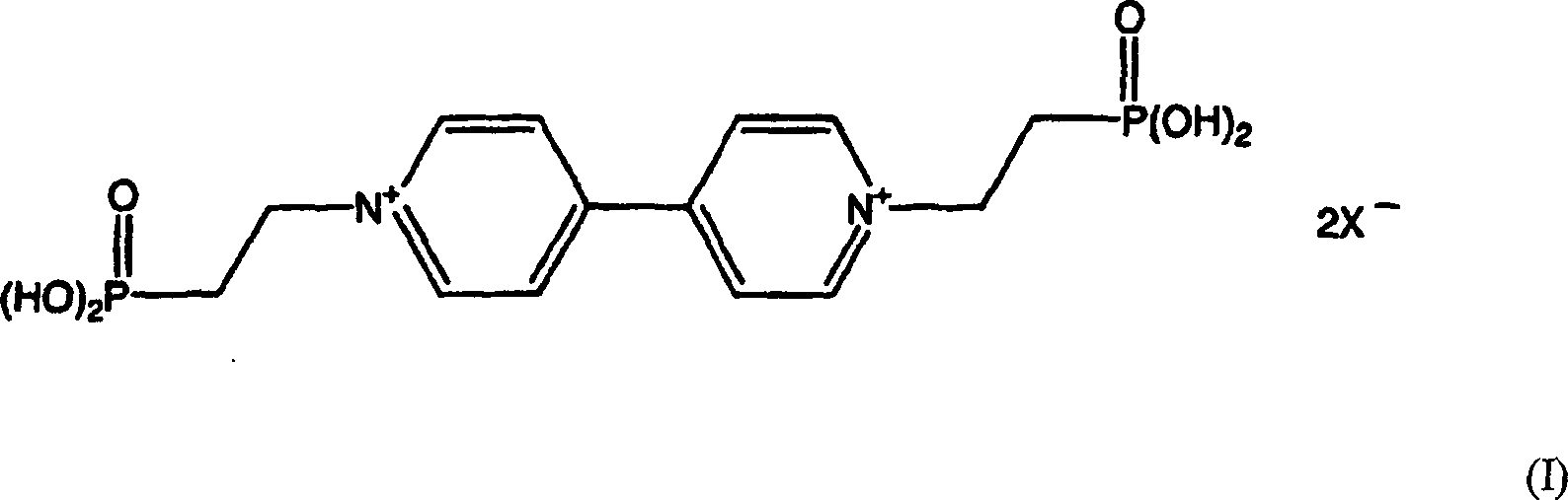
Ein "nanokristalliner Film" besteht aus verschmolzenen Kristalliten im Nanometer-Bereich. Bei einem "nanoporös-nanokristallinen" Film ist die Morphologie der verschmolzenen Nanokristallite so beschaffen, dass sie im Nanometer-Bereich porös ist. Derartige Filme, die im Folgenden als nanostrukturierte Filme bezeichnet werden können, besitzen typischerweise eine Oberflächenrauhigkeit von etwa 1000, wobei eine Dicke von etwa 10 μm angenommen wird.A "nanocrystalline Film "consists of fused crystallites in the nanometer range. In a "nanoporous-nanocrystalline" film is the morphology of the fused nanocrystallites so that they are in the nanometer range is porous. Such films, which are referred to below as nanostructured films can, typically have a surface roughness of about 1000, wherein a thickness of about 10 microns Is accepted.
Die in der vorliegenden Erfindung verwendeten nanostrukturierten Filme färben sich beim Anlegen eines Potenzials, das ausreichend negativ ist, um Elektronen in den verfügbaren Haftstellen- und Leitungsbandzuständen zu sammeln. Als Folge der hohen Oberflächenrauhigkeit dieser Filme werden Ionen leicht an der Oxidfläche adsorbiert/interpoliert, wodurch ein wirksamer Ladungsausgleich und ein schnelles Schalten ermöglicht werden, d.h. der Bedarf für Masseninterpolation wird beseitigt. Trotz der schnellen Schaltzeiten bei diesen Filmen reicht die zugehörige Änderung des Durchlässigkeitsgrads für eine kommerzielle Vorrichtung jedoch nicht aus. Um diese Beschränkung zu überwinden, wird ein Redox-Chromophor an der Oberfläche des transparenten nanostrukturierten Films adsorbiert, der, wenn er reduziert ist, den Extinktionskoeffizienten eines angesammelten Haft- oder Leitungsbandelektrons um mehr als eine Größenordnung vergrößert. Des Weiteren wird aufgrund der nanoporösen Struktur und zugehörigen Oberflächenrauhigkeit der verwendeten nanokristallinen Filme das Redox-Chromophor wie in einem Polymerfilm wirksam übereinandergeschichtet, während es gleichzeitig den engen Kontakt mit dem Metalloxidsubstrat aufrecht erhält, der zur Sicherstellung der schnellen Schaltzeiten notwendig ist.The nanostructured films used in the present invention to dye when creating a potential that is sufficiently negative around electrons in the available Collect trap and conduction band states. As a result the high surface roughness of these films, ions are easily adsorbed / interpolated on the oxide surface, whereby an effective charge balance and a fast switching allows are, i. the need for Mass interpolation is eliminated. Despite the fast switching times in these films, the associated change in transmittance is sufficient for one However, commercial device is not enough. To overcome this limitation, becomes a redox chromophore on the surface of the transparent nanostructured Adsorbs film which, when reduced, the extinction coefficient of accumulated traction or conduction band electrons by more than an order of magnitude increased. Of Further, due to the nanoporous structure and associated surface roughness the nanocrystalline films used the redox chromophore as in a polymer film effectively stacked, while At the same time it maintains the close contact with the metal oxide substrate gets which is necessary to ensure the fast switching times.
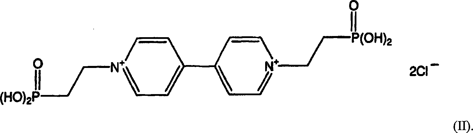
Ein besonders bevorzugtes Redox-Chromophor ist eine Verbindung nach Formel II, d.h. Bis-(2-phosphono-ethyl)-4,4'-bipyridinium-dichloridOne Particularly preferred redox chromophore is a compound according to Formula II, i. Bis- (2-phosphono-ethyl) -4,4'-bipyridinium dichloride
Das halbleitende Metalloxid kann ein Oxid aus einem geeigneten Metall sein, zum Beispiel Titan, Zirconium, Hafnium, Chrom, Molybdän, Wolfram, Vanadium, Niob, Tantal, Silber, Zink, Strontium, Eisen (Fe2+ oder Fe3+) oder Nickel oder ein Perovskit davon. TiO2, WO3, MoO3, ZnO und SnO2 werden besonders bevorzugt.The semiconductive metal oxide may be an oxide of a suitable metal, for example, titanium, zirconium, hafnium, chromium, molybdenum, tungsten, vanadium, niobium, tantalum, silver, zinc, strontium, iron (Fe 2+ or Fe 3+ ) or nickel or a perovskite of it. TiO 2 , WO 3 , MoO 3 , ZnO and SnO 2 are particularly preferred Trains t.
Die Erfindung schafft ebenfalls ein elektrochromes System, das Folgendes umfasst: eine erste Elektrode, die auf einem transparenten oder transluzenten Substrat angeordnet ist; eine zweite Elektrode; einen Elektrolyt; einen Elektronen-Donator und eine elektrochrome Schicht, die einen nanoporös-nanokristallinen Film gemäß der Erfindung zwischen der ersten und zweiten Elektrode umfasst.The The invention also provides an electrochromic system which has the following includes: a first electrode on a transparent or translucent substrate is arranged; a second electrode; an electrolyte; an electron donor and an electrochromic layer containing a nanoporous nanocrystalline film according to the invention between the first and second electrodes.
Das Substrat ist geeigneterweise aus einem Glas- oder Kunststoffmaterial gebildet. Angemessenerweise wird Glas, das mit einer leitenden Schicht aus fluordotiertem Zinnoxid oder Indiumzinnoxid beschichtet ist, in dem EC-System der vorliegenden Erfindung verwendet.The Substrate is suitably made of a glass or plastic material educated. Appropriately, glass is covered with a conductive layer is coated from fluorine doped tin oxide or indium tin oxide, used in the EC system of the present invention.
Der Elektrolyt liegt vorzugsweise in flüssiger Form vor und umfasst vorzugsweise mindestens ein elektrochemisch inertes Salz, optional in geschmolzener Form oder in Lösung in einem Lösungsmittel. Beispiele für geeignete Salze umfassen Hexafluorphosphat, Bis-trifluormethansulfonat, Bis-trifluormethyl-sulfonylimid, Tetraalkylammonium, Dialkyl-1,3-imidazolium und Lithiumperchlorat. Beispiele für geeignete geschmolzene Salze umfassen Trifluormethansulfonat, 1-Ethyl,3-methyl-imidazolium-bis-trifluormethyl-sulfonylimid und 1-Propyldimethylimidazolium-bis-trifluormethyl-sulfonylimid. Lithiumperchlorat wird besonders bevorzugt.Of the Electrolyte is preferably in liquid form and comprises preferably at least one electrochemically inert salt, optional in molten form or in solution in a solvent. examples for suitable salts include hexafluorophosphate, bis-trifluoromethanesulfonate, Bis-trifluoromethyl-sulfonylimide, tetraalkylammonium, dialkyl-1,3-imidazolium and lithium perchlorate. Examples of suitable molten salts include trifluoromethanesulfonate, 1-ethyl, 3-methyl-imidazolium-bis-trifluoromethyl-sulfonyl-imide and 1-propyl-dimethylimidazolium-bis-trifluoromethyl-sulfonyl-imide. Lithium perchlorate is particularly preferred.
Das Lösungsmittel kann jedes geeignete Lösungsmittel sein und wird vorzugsweise aus Folgendem ausgewählt: Acetonitril, Butyronitril, Glutaronitril, Dimethylsulfoxid, Dimethylformamid, Dimethylacetamid, N-Methyloxazolidinon, Dimethyltetrahydropyrimidinon und γ-Butyrolacton sowie Mischungen daraus.The solvent can be any suitable solvent and is preferably selected from the following: acetonitrile, butyronitrile, Glutaronitrile, dimethyl sulfoxide, dimethylformamide, dimethylacetamide, N-methyl oxazolidinone, Dimethyltetrahydropyrimidinone and γ-butyrolactone and mixtures it.
Der Elektronendonator ist vorzugsweise ein Metallocen oder ein Derivat davon. Der Elektronendonator ist vorzugsweise in dem Elektrolytlösungsmittel löslich. Ferrocen wird besonders bevorzugt.Of the Electron donor is preferably a metallocene or a derivative from that. The electron donor is preferably in the electrolyte solvent soluble. Ferrocene is particularly preferred.
Die Erfindung wird in dem folgenden Beispiel veranschaulicht.The Invention is illustrated in the following example.
BEISPIELEXAMPLE
- (a) Ein transparenter nanostrukturierter Film mit einer Größe von 2,5 cm × 2,5 cm, der aus einer 4 μm dicken Schicht aus verschmolzenen TiO2-Nanokristalliten bestand, wurde auf einem fluordotierten Zinnoxid auf einem Glassubstrat (Glastron, Handelsmarke) mit einer Größe von 3,3 cm × 3,3 cm aufgetragen. Eine kolloidale TiO2-Dispersion wurde durch Hydrolyse von Titantetraisopropoxid hergestellt. Der durchschnittliche Durchmesser der anfänglich gebildeten Kristallite (7 nm) wurde durch Autoklavieren bei 200°C für 12 Stunden auf 12 nm vergrößert. Durch Konzentrieren der autoklavierten Dispersion auf 160 g/l und die Hinzugabe von Carbowax (Handelsmarke) 20.000 (40 Gew.-% äquivalent zu TiO2) wurde ein weißes viskoses Sol erzeugt. (Carbowax 20.000 ist ein Ethylenglykolpolymer, dessen durchschnittliches Molekulargewicht 20.000 beträgt.) Eine 4 μm dicke Schicht des oben genannten Sols wurde unter Verwendung eines Siebdruckverfahrens auf das leitfähige Glassubstrat aufgetragen. Der resultierende Gelfilm wurde etwa 1 Std. lang an der Luft getrocknet, bei 450°C 12 Std. lang gesintert und vor der Verwendung in einem verdunkelten Vakuumtrockenapparat gelagert.(a) A 2.5 cm x 2.5 cm transparent nanostructured film consisting of a 4 μm thick layer of fused TiO 2 nanocrystallites was supported on a fluorine-doped tin oxide on a glass substrate (Glastron, Trademark) a size of 3.3 cm × 3.3 cm applied. A colloidal TiO 2 dispersion was prepared by hydrolysis of titanium tetraisopropoxide. The average diameter of the initially formed crystallites (7 nm) was increased to 12 nm by autoclaving at 200 ° C for 12 hours. Concentrating the autoclaved dispersion to 160 g / L and adding Carbowax (Trade Mark) 20,000 (40 wt.% Equivalent to TiO 2 ) produced a white viscous sol. (Carbowax 20,000 is an ethylene glycol polymer whose average molecular weight is 20,000.) A 4 μm thick layer of the above sol was applied to the conductive glass substrate using a screen printing method. The resulting gel film was air-dried for about 1 hr, sintered at 450 ° C for 12 hr, and stored in a darkened vacuum dryer prior to use.
- (b) Ein Redox-Chromophor, Bis-(2-phosphonoethyl)-4,4'-bipyridiniumdichlorid, wurde unter Hinzugabe von 4,4'-Bipyridin (4,4 g) und Diethyl-2-ethylbromphosphonat (15,0 g) zu Wasser (75 ml) hergestellt. Das Reaktionsgemisch lief 72 Std. lang zurück und wurde abgekühlt. Nach der Hinzugabe von konzentrierter Chlorwasserstoffsäure (75 ml) lief das Reaktionsgemisch weitere 24 Std. zurück. Zur Rückgewinnung des Produkts wurde das Reaktionsgemisch auf 50 ml konzentriert, es wurde Isopropylalkohol (200 ml) tropfenweise hinzugefügt und auf Eis eine Stunde lang umgerührt und gefiltert. Das weiße kristalline Produkt wurde mit kaltem Isopropylalkohol gewaschen und luftgetrocknet, um reines Bis-(2-phosphonoethyl)-4,4'-bipyridiniumdichlorid zu ergeben (12,72 g; 84,24%iger Ertrag). Berechnet für Bis-(2-phosphonoethyl)-4,4'-bipyridiniumdichlorid (C14H20N2Cl2O6P2): C: 37,77; H: 4,53; N: 6,29. Vorgefunden: C: 35,09; H: 4,49; N: 6,09. 1H NMR (Wasser-d2): δ 2,31–2,43 (m, 4H); δ 4,68–4,80 (m, 4H); δ 8,33 (d, nicht aufgelöste Metaverbindung, 4H); δ 8,94 (d, nicht aufgelöste Metaverbindung, 4H).(b) A redox chromophore, bis (2-phosphonoethyl) -4,4'-bipyridinium dichloride, was added with the addition of 4,4'-bipyridine (4.4 g) and diethyl 2-ethylbromophosphonate (15.0 g ) to water (75 ml). The reaction was refluxed for 72 h and was cooled. After the addition of concentrated hydrochloric acid (75 ml), the reaction mixture refluxed for a further 24 hours. To recover the product, the reaction mixture was concentrated to 50 ml, added dropwise isopropyl alcohol (200 ml) and stirred on ice for one hour and filtered. The white crystalline product was washed with cold isopropyl alcohol and air dried to give pure bis- (2-phosphonoethyl) -4,4'-bipyridinium dichloride (12.72 g, 84.24% yield). Calculated for bis (2-phosphonoethyl) -4,4'-bipyridinium dichloride (C 14 H 20 N 2 Cl 2 O 6 P 2 ): C, 37.77; H: 4.53; N: 6.29. Found: C: 35.09; H: 4.49; N: 6.09. 1 H NMR (water-d 2 ): δ 2.31-2.43 (m, 4H); δ 4.68-4.80 (m, 4H); δ 8.33 (d, unresolved meta compound, 4H); δ 8.94 (d, unresolved meta compound, 4H).
- (c) TiO2-Filme, die wie oben beschrieben hergestellt wurden, wurden durch Adsorption des Redox-Chromophors, das oben aus einer wässrigen Lösung (0,02 mol/dm–3) über einen Zeitraum von 24 Std. hergestellt wurde, modifiziert, mit destilliertem deionisiertem Wasser gewaschen, an der Luft getrocknet und in einem verdunkelten Vakuumexsikkator vor Gebrauch 48 Std. lang gelagert.(c) TiO 2 films prepared as described above were modified by adsorption of the redox chromophore prepared above from an aqueous solution (0.02 mol / dm -3 ) over a period of 24 hours , washed with distilled deionized water, air dried and stored in a darkened vacuum desiccator for 48 hours prior to use.
- (d) Unter Verwendung eines Siebdruckverfahrens wurde ein Rand von 0,25 cm eines patentrechtlich geschützten Epoxidharzes (Araldit, Handelsname) auf einem zweiten leitfähigen fluordotierten Zinnoxidglas mit einer Größe von 3,3 × 3,3 cm aufgetragen, wobei eine kleine Öffnung in einer Ecke belassen wurde. Dieses Stück leitfähiges Glas wurde auf dem modifizierten TiO2-Film angeordnet, der wie oben beschrieben hergestellt wurde, und härtete 24 Std. lang aus.(d) Using a screen printing process, a 0.25 cm edge of a proprietary epoxy resin (Araldit, trade name) was applied to a second conductive fluorine-doped tin oxide glass of 3.3 x 3.3 cm size, with a small opening in one Corner was left. This piece of conductive glass was placed on the modified TiO 2 film as described above and cured for 24 hrs.
- (e) Um die Konstruktion des EC-Systems zu vervollständigen, wurde die oben genannte Schichtkonstruktion unter Verwendung eines Argondrucks mit einer Elektrolytlösung hinterfüllt, die aus LiClO4 (0,05 mol/dm–3) und Ferrocen (0,05 mol/dm–3) in γ-Butyrolacton (Schmelzpunkt –45°C, Siedepunkt 204°C) bestand. Die Komponenten der Elektrolytlösung wurden vor der Verwendung sorgfältig gereinigt und rigoros getrocknet. Die Öffnung wurde daraufhin unter Verwendung von Araldit (Handelsname) verschlossen.(e) In order to complete the construction of the EC system, the above-mentioned layer construction was back-filled using an argon pressure with an electrolytic solution consisting of LiClO 4 (0.05 mol / dm -3 ) and ferrocene (0.05 mol / dm -3 ) in γ-butyrolactone (melting point -45 ° C, boiling point 204 ° C). The components of the electrolyte solution were thoroughly cleaned before use and dried rigorously. The opening was then closed using Araldit (trade name).
Das
EC-System, das wie in dem Beispiel hergestellt wurde, ist in
Unter
Bezugnahme auf die Zeichnungen und insbesondere auf
Es
ist ersichtlich, dass die Konstruktion des EC-Systems
Es wird weiterhin angemerkt, dass aufgrund der Oberflächenrauhigkeit in der Größenordnung von 500 für einen Film mit einer Dicke von 4 μm bei einem EC-System der Erfindung kein Abstandshalter erforderlich ist.It is further noted that due to the surface roughness in the order of magnitude from 500 for a film with a thickness of 4 microns no spacer is required in an EC system of the invention.
Bei elektrochromen Systemen des Stands der Technik muss ein dielektrischer Abstandshalter enthalten sein, um die Elektroden elektrisch voneinander zu isolieren. Bei der vorliegenden Erfindung ist kein derartiger Abstandshalter erforderlich, da die Beschaffenheit des nanokristallinen Films als Festpartikel eine ausreichende elektrische Isolierung zwischen den Elektroden bereitstellt. Bei einer kommerziellen Version des EC-Systems gemäß der Erfindung hat die Abwesenheit eines Abstandshalters einen positiven Einfluss auf die Herstellungskosten des Systems.at electrochromic systems of the prior art must be a dielectric Spacers may be included to electrically separate the electrodes from each other to isolate. In the present invention is not such Spacers required because of the nature of the nanocrystalline Films as solid particles sufficient electrical insulation between the electrodes. In a commercial version of the EC system according to the invention the absence of a spacer has a positive influence on the manufacturing cost of the system.
Eine
Reihe von EC-Systemen, die wie in dem oben genannten Beispiel hergestellt
wurden, wurde durch Durchführen
von 10.000 Zyklen (15 sek bei –1,00
V und 15 sek bei +1,0 V bei Raumtemperatur) getestet. Ein typischer
Satz von Testergebnissen ist in
Insbesondere
sind in
Was
die Änderung
des Durchlässigkeitsgrads
angeht, so wird diese herkömmlicherweise
wie in
Wie
erwähnt,
besteht keine bedeutende Leistungsverschlechterung nach 10.000 Zyklen.
Dies wird quantitativ in
Nanostrukturierte
TiO2-Filme wurden auf den folgenden leitenden
Glassubstraten aufgetragen: Indiumzinnoxidglas und fluordotiertes
Zinnoxidglas. Es wurde kein bedeutender Leistungsunterschied bei
dem resultierenden EC-System bemerkt. Die Zeit, für die ein
Film gebrannt wird, ist aus folgenden Gründen von Bedeutung:
Wenn
ein Film 1 Std. lang gebrannt wird, ist seine Porosität und folglich
seine Oberflächenrauhigkeit
optimal. Unter denselben Bedingungen ist die Filmleitfähigkeit
aufgrund von unvollständigem
Sintern der Nanokristallite, die die Bestandteile bilden, jedoch
weniger als optimal. Umgekehrt sind die Konnektivität und folglich
die Leitfähigkeit
eines Films, der 168 Std. gebrannt wird, optimal.Nanostructured TiO 2 films were deposited on the following conductive glass substrates: indium tin oxide glass and fluorine doped tin oxide glass. No significant performance difference was noted in the resulting EC system. The time a movie is burned is important for the following reasons:
When a film is baked for one hour, its porosity and hence its surface roughness are optimal. However, under the same conditions, film conductivity is less than optimal due to incomplete sintering of the nanocrystallites that make up the components. Conversely, the connectivity, and hence the conductivity, of a 168-hr film is optimal.
Unter
denselben Bedingungen ist jedoch die Filmporosität aufgrund eines Zusammenbruchs
der Nanostruktur des Films weniger als optimal, wie aus
Die Filmbrenntemperatur sollte mehr als 400°C betragen, um das hinzugefügte Carbowax zu entfernen, dessen Zugabe für die Sicherstellung eines porösen Films wesentlich ist, und sie sollte weniger als 500°C betragen, um die Umwandlung von Anatas in Rutil zu verhindern, wobei Letzteres ein wesentlich schlechterer Leiter ist. Aus diesen Gründen wurde die Brenntemperatur bei etwa 450°C festgelegt.The Film firing temperature should be more than 400 ° C to add the added Carbowax to remove, its addition for ensuring a porous Film is essential and should be less than 500 ° C, to prevent the conversion of anatase into rutile, the latter is a much worse leader. For these reasons was the firing temperature at about 450 ° C established.
Die Substituentengruppen des Redox-Chromophors werden an Ti4+-Stellen an der Oberfläche der TiO2-Nanokristallite, die den nanoporös-nanokristallinen Film bilden, unumkehrbar chemisorbiert. Diese Substituentengruppen, die als Verknüpfergruppen bezeichnet werden, dienen daher dazu, das Redox-Chromophor unumkehrbar mit der Oberfläche des nanoporös-nanokristallinen Films zu verbinden. Die Dichte dieser Zustände (etwa 5 × 1013 cm–2) und die Oberflächenrauhigkeit (etwa 1000 für einen 4 μm Film) stellen die obere Grenze für die Anzahl molekularer Verstärker dar, die pro geometrischem Einheitsbereich adsorbiert werden können. Es wird ebenfalls darauf hingewiesen, dass im Gegensatz zu Verknüpfern des Stands der Technik keine Entfärbung des modifizierten Films aufgrund des Bestehens einer Ladungsübertragungswechselwirkung zwischen den besetzten Molekularumlaufbahnen des Verknüpfers und dem genannten verfügbaren Leitungsband des Halbleitersubstrats vorliegt. In Bezug auf das Redox-Chromophor ist der Viologenrest stabil bei einer großen zugehörigen Änderung der Extinktion für eine Ein-Elektron-Reduktion. Des Weiteren kann das Redox-Chromophor durch die Verwendung der verschiedenen Substituenten, die in der allgemeinen Formel zu R gehören, leicht derart modifiziert werden, dass es seine elektrochemischen und optischen Eigenschaften ändert. Jede Variation besitzt andere formale Potenziale und andere Farben beim Schalten. Des Weiteren kann das Redox-Chromophor leicht mit einer hohen Ergiebigkeit in einer reinen Form hergestellt werden und, was vielleicht das Wichtigste ist, von einer wässrigen Lösung auf das TiO2-Substrat adsorbiert werden.The substituent groups of the redox chromophore are irreversibly chemisorbed at Ti 4+ sites on the surface of the TiO 2 nanocrystallites that form the nanoporous nanocrystalline film. These substituent groups, referred to as linker groups, therefore serve to irreversibly link the redox chromophore to the surface of the nanoporous nanocrystalline film. The density of these states (about 5 × 10 13 cm -2 ) and the surface roughness (about 1000 for a 4 μm film) represent the upper limit to the number of molecular amplifiers that can be adsorbed per unit geometric area. It is also noted that, unlike prior art linkers, there is no discoloration of the modified film due to the existence of a charge transfer interaction between the occupied molecular orbits of the linker and said available conduction band of the semiconductor substrate. With respect to the redox chromophore, the viologen residue is stable with a large accompanying change in absorbance for one-electron reduction. Furthermore, the use of the various substituents belonging to R in the general formula can easily modify the redox chromophore to alter its electrochemical and optical properties. Each variation has different formal potentials and other colors when switching. Furthermore, the redox chromophore can be easily produced with high yield in a pure form and, perhaps most importantly, adsorbed onto the TiO 2 substrate by an aqueous solution.
Ein
Parameter, der hinsichtlich des Redox-Chromophors untersucht wurde,
war das Ausmaß der
Modifikatoradsorption über
einen gegebenen Zeitraum. Wie erwartet werden würde, wird das Redox-Chromophor in
zunehmendem Ausmaß von
konzentrierteren Lösungen
in kürzerer
Zeit adsorbiert. In der Praxis wird für eine wässrige 0,02 mol/dm–3 Lösung des
Redox-Chromophors eine nahezu maximale Abdeckung nach etwa 6 Std.
bei nur geringer nachfolgender Zunahme der Abdeckung während der
darauffolgenden Woche beobachtet, siehe
Die
Konzentration von hinzugefügtem
LiClO4 im Bereich von 0,05 mol/dm–3 bis
0,20 mol/dm–3 hat
keine Wirkung auf die Größenordnung
der Änderung
des Durchlässigkeitsgrads
oder auf die Färbungs-
oder Aufklärungszeiten
(siehe
Die
Legenden für
Claims (14)

Applications Claiming Priority (3)
| Application Number | Priority Date | Filing Date | Title |
|---|---|---|---|
| IE970082 | 1997-02-06 | ||
| IE970082 | 1997-02-06 | ||
| PCT/IE1998/000008 WO1998035267A1 (en) | 1997-02-06 | 1998-02-06 | Electrochromic system |
Publications (2)
| Publication Number | Publication Date |
|---|---|
| DE69830566D1 DE69830566D1 (en) | 2005-07-21 |
| DE69830566T2 true DE69830566T2 (en) | 2006-05-11 |
Family
ID=11041368
Family Applications (1)
| Application Number | Title | Priority Date | Filing Date |
|---|---|---|---|
| DE69830566T Expired - Lifetime DE69830566T2 (en) | 1997-02-06 | 1998-02-06 | ELECTROCHROMIC SYSTEM |
Country Status (7)
| Country | Link |
|---|---|
| US (4) | US6301038B1 (en) |
| EP (1) | EP0958526B1 (en) |
| JP (1) | JP3955641B2 (en) |
| AT (1) | ATE298098T1 (en) |
| AU (1) | AU6004798A (en) |
| DE (1) | DE69830566T2 (en) |
| WO (1) | WO1998035267A1 (en) |
Families Citing this family (355)
| Publication number | Priority date | Publication date | Assignee | Title |
|---|---|---|---|---|
| US7956841B2 (en) | 1995-07-20 | 2011-06-07 | E Ink Corporation | Stylus-based addressing structures for displays |
| US7193625B2 (en) | 1999-04-30 | 2007-03-20 | E Ink Corporation | Methods for driving electro-optic displays, and apparatus for use therein |
| US7999787B2 (en) | 1995-07-20 | 2011-08-16 | E Ink Corporation | Methods for driving electrophoretic displays using dielectrophoretic forces |
| US8139050B2 (en) | 1995-07-20 | 2012-03-20 | E Ink Corporation | Addressing schemes for electronic displays |
| US8089453B2 (en) | 1995-07-20 | 2012-01-03 | E Ink Corporation | Stylus-based addressing structures for displays |
| US7079305B2 (en) | 2001-03-19 | 2006-07-18 | E Ink Corporation | Electrophoretic medium and process for the production thereof |
| US7848006B2 (en) | 1995-07-20 | 2010-12-07 | E Ink Corporation | Electrophoretic displays with controlled amounts of pigment |
| US7327511B2 (en) | 2004-03-23 | 2008-02-05 | E Ink Corporation | Light modulators |
| US7411719B2 (en) | 1995-07-20 | 2008-08-12 | E Ink Corporation | Electrophoretic medium and process for the production thereof |
| US7259744B2 (en) * | 1995-07-20 | 2007-08-21 | E Ink Corporation | Dielectrophoretic displays |
| US7583251B2 (en) * | 1995-07-20 | 2009-09-01 | E Ink Corporation | Dielectrophoretic displays |
| DE69830566T2 (en) * | 1997-02-06 | 2006-05-11 | University College Dublin | ELECTROCHROMIC SYSTEM |
| US7247379B2 (en) | 1997-08-28 | 2007-07-24 | E Ink Corporation | Electrophoretic particles, and processes for the production thereof |
| US7002728B2 (en) | 1997-08-28 | 2006-02-21 | E Ink Corporation | Electrophoretic particles, and processes for the production thereof |
| US8040594B2 (en) | 1997-08-28 | 2011-10-18 | E Ink Corporation | Multi-color electrophoretic displays |
| US8213076B2 (en) | 1997-08-28 | 2012-07-03 | E Ink Corporation | Multi-color electrophoretic displays and materials for making the same |
| DE19756740A1 (en) * | 1997-12-19 | 1999-06-24 | Bayer Ag | Electrochromic device is protected against UV light by nano particles |
| ATE349722T1 (en) | 1998-07-08 | 2007-01-15 | E Ink Corp | IMPROVED COLOR MICRO-ENCAPSULED ELECTROPHORETIC DISPLAY |
| DE59911011D1 (en) | 1998-09-08 | 2004-12-09 | Bayer Chemicals Ag | ELECTROCHROME DEVICE WITH YELLOW FILTER |
| DE19914093A1 (en) * | 1999-03-27 | 2000-10-19 | Dornier Gmbh | Electrochromic element |
| US7012600B2 (en) | 1999-04-30 | 2006-03-14 | E Ink Corporation | Methods for driving bistable electro-optic displays, and apparatus for use therein |
| US7119772B2 (en) | 1999-04-30 | 2006-10-10 | E Ink Corporation | Methods for driving bistable electro-optic displays, and apparatus for use therein |
| US7119759B2 (en) | 1999-05-03 | 2006-10-10 | E Ink Corporation | Machine-readable displays |
| US8115729B2 (en) | 1999-05-03 | 2012-02-14 | E Ink Corporation | Electrophoretic display element with filler particles |
| US8009348B2 (en) | 1999-05-03 | 2011-08-30 | E Ink Corporation | Machine-readable displays |
| JP4744757B2 (en) | 1999-07-21 | 2011-08-10 | イー インク コーポレイション | Use of storage capacitors to enhance the performance of active matrix driven electronic displays. |
| EP1500969A1 (en) * | 1999-10-11 | 2005-01-26 | University College Dublin | Compound and its use in electrochromic devices |
| US6266177B1 (en) | 1999-11-18 | 2001-07-24 | Donnelly Corporation | Electrochromic devices |
| US6614578B2 (en) | 1999-12-03 | 2003-09-02 | Gentex Corporation | Ultraviolet stabilizing materials having a solublizing moiety |
| US6700693B2 (en) | 1999-12-03 | 2004-03-02 | Gentex Corporation | Electrochromic devices having an electron shuttle |
| US6262832B1 (en) | 1999-12-03 | 2001-07-17 | Gentex Corporation | Anodic electrochromic materials having a solublizing moiety |
| US6710906B2 (en) | 1999-12-03 | 2004-03-23 | Gentex Corporation | Controlled diffusion coefficient electrochromic materials for use in electrochromic mediums and associated electrochromic devices |
| US7893435B2 (en) | 2000-04-18 | 2011-02-22 | E Ink Corporation | Flexible electronic circuits and displays including a backplane comprising a patterned metal foil having a plurality of apertures extending therethrough |
| DE60139463D1 (en) | 2000-04-18 | 2009-09-17 | E Ink Corp | PROCESS FOR THE MANUFACTURE OF THIN FILM TRANSISTORS |
| SE518964C2 (en) * | 2000-08-03 | 2002-12-10 | Gerrit Boschloo | Container device for storing hazardous material and methods for its preparation |
| US6816147B2 (en) | 2000-08-17 | 2004-11-09 | E Ink Corporation | Bistable electro-optic display, and method for addressing same |
| EP1340360A2 (en) * | 2000-12-05 | 2003-09-03 | E Ink Corporation | Portable electronic apparatus with additional electro-optical display |
| JP4198999B2 (en) | 2001-03-13 | 2008-12-17 | イー インク コーポレイション | Equipment for displaying drawings |
| US20050156340A1 (en) | 2004-01-20 | 2005-07-21 | E Ink Corporation | Preparation of capsules |
| US7679814B2 (en) | 2001-04-02 | 2010-03-16 | E Ink Corporation | Materials for use in electrophoretic displays |
| US8390918B2 (en) | 2001-04-02 | 2013-03-05 | E Ink Corporation | Electrophoretic displays with controlled amounts of pigment |
| US7230750B2 (en) | 2001-05-15 | 2007-06-12 | E Ink Corporation | Electrophoretic media and processes for the production thereof |
| US6580545B2 (en) * | 2001-04-19 | 2003-06-17 | E Ink Corporation | Electrochromic-nanoparticle displays |
| EP1393122B1 (en) | 2001-05-15 | 2018-03-28 | E Ink Corporation | Electrophoretic particles |
| SE522614C2 (en) * | 2001-06-05 | 2004-02-24 | Ivf Industriforskning Och Utve | Electrochrome display with a porous nanostructured electrode and method for manufacturing electrochrome display |
| EP1271227A1 (en) * | 2001-06-26 | 2003-01-02 | Nanomat Limited | Electrochromic display for high resolution and method of producing the same |
| US6982178B2 (en) | 2002-06-10 | 2006-01-03 | E Ink Corporation | Components and methods for use in electro-optic displays |
| ATE549659T1 (en) * | 2001-07-09 | 2012-03-15 | E Ink Corp | ELECTRO-OPTICAL DISPLAY DEVICE WITH LAMINATE ADHESIVE LAYER |
| JP2004535599A (en) * | 2001-07-09 | 2004-11-25 | イー−インク コーポレイション | Electro-optical display and adhesive composition |
| US7535624B2 (en) | 2001-07-09 | 2009-05-19 | E Ink Corporation | Electro-optic display and materials for use therein |
| US7110163B2 (en) | 2001-07-09 | 2006-09-19 | E Ink Corporation | Electro-optic display and lamination adhesive for use therein |
| AU2002365115A1 (en) * | 2001-07-20 | 2003-09-02 | North Carolina State University | Light addressable electrochemical detection of duplex structures |
| US6967640B2 (en) | 2001-07-27 | 2005-11-22 | E Ink Corporation | Microencapsulated electrophoretic display with integrated driver |
| US6825970B2 (en) * | 2001-09-14 | 2004-11-30 | E Ink Corporation | Methods for addressing electro-optic materials |
| US8558783B2 (en) | 2001-11-20 | 2013-10-15 | E Ink Corporation | Electro-optic displays with reduced remnant voltage |
| US7952557B2 (en) | 2001-11-20 | 2011-05-31 | E Ink Corporation | Methods and apparatus for driving electro-optic displays |
| US8125501B2 (en) | 2001-11-20 | 2012-02-28 | E Ink Corporation | Voltage modulated driver circuits for electro-optic displays |
| CN102789758B (en) | 2001-11-20 | 2016-05-18 | 伊英克公司 | Drive the method for bistable electro-optic displays |
| US9530363B2 (en) | 2001-11-20 | 2016-12-27 | E Ink Corporation | Methods and apparatus for driving electro-optic displays |
| US8593396B2 (en) | 2001-11-20 | 2013-11-26 | E Ink Corporation | Methods and apparatus for driving electro-optic displays |
| US9412314B2 (en) | 2001-11-20 | 2016-08-09 | E Ink Corporation | Methods for driving electro-optic displays |
| US7528822B2 (en) | 2001-11-20 | 2009-05-05 | E Ink Corporation | Methods for driving electro-optic displays |
| WO2003058692A1 (en) * | 2001-12-28 | 2003-07-17 | University And Community College System Of Nevada On Behalf Of The University Of Nevada, Reno | Redox-switchable materials |
| US6950220B2 (en) | 2002-03-18 | 2005-09-27 | E Ink Corporation | Electro-optic displays, and methods for driving same |
| US7190008B2 (en) | 2002-04-24 | 2007-03-13 | E Ink Corporation | Electro-optic displays, and components for use therein |
| US7223672B2 (en) | 2002-04-24 | 2007-05-29 | E Ink Corporation | Processes for forming backplanes for electro-optic displays |
| AU2003232018A1 (en) | 2002-04-24 | 2003-11-10 | E Ink Corporation | Electronic displays |
| US6958848B2 (en) | 2002-05-23 | 2005-10-25 | E Ink Corporation | Capsules, materials for use therein and electrophoretic media and displays containing such capsules |
| US7554712B2 (en) | 2005-06-23 | 2009-06-30 | E Ink Corporation | Edge seals for, and processes for assembly of, electro-optic displays |
| US7583427B2 (en) | 2002-06-10 | 2009-09-01 | E Ink Corporation | Components and methods for use in electro-optic displays |
| US7649674B2 (en) | 2002-06-10 | 2010-01-19 | E Ink Corporation | Electro-optic display with edge seal |
| US8049947B2 (en) | 2002-06-10 | 2011-11-01 | E Ink Corporation | Components and methods for use in electro-optic displays |
| US7843621B2 (en) | 2002-06-10 | 2010-11-30 | E Ink Corporation | Components and testing methods for use in the production of electro-optic displays |
| US9470950B2 (en) | 2002-06-10 | 2016-10-18 | E Ink Corporation | Electro-optic displays, and processes for the production thereof |
| US7110164B2 (en) | 2002-06-10 | 2006-09-19 | E Ink Corporation | Electro-optic displays, and processes for the production thereof |
| US8363299B2 (en) | 2002-06-10 | 2013-01-29 | E Ink Corporation | Electro-optic displays, and processes for the production thereof |
| AU2003239619A1 (en) | 2002-06-13 | 2003-12-31 | E Ink Corporation | Methods for driving electro-optic displays |
| US20080024482A1 (en) | 2002-06-13 | 2008-01-31 | E Ink Corporation | Methods for driving electro-optic displays |
| US6961168B2 (en) * | 2002-06-21 | 2005-11-01 | The Regents Of The University Of California | Durable electrooptic devices comprising ionic liquids |
| US7450292B1 (en) * | 2003-06-20 | 2008-11-11 | Los Alamos National Security, Llc | Durable electrooptic devices comprising ionic liquids |
| US7312916B2 (en) | 2002-08-07 | 2007-12-25 | E Ink Corporation | Electrophoretic media containing specularly reflective particles |
| JP4564355B2 (en) * | 2002-09-03 | 2010-10-20 | イー インク コーポレイション | Electrophoretic medium with gaseous suspension fluid |
| US7839564B2 (en) | 2002-09-03 | 2010-11-23 | E Ink Corporation | Components and methods for use in electro-optic displays |
| CN100397227C (en) * | 2002-09-03 | 2008-06-25 | 伊英克公司 | Electrophoretic medium and method of forming electrophoretic medium |
| TWI300157B (en) * | 2002-09-10 | 2008-08-21 | Sipix Imaging Inc | Electrochromic or electrodeposition display and process for their preparation |
| US20130063333A1 (en) | 2002-10-16 | 2013-03-14 | E Ink Corporation | Electrophoretic displays |
| AU2003299673A1 (en) | 2002-12-16 | 2004-07-22 | E Ink Corporation | Backplanes for electro-optic displays |
| US6922276B2 (en) * | 2002-12-23 | 2005-07-26 | E Ink Corporation | Flexible electro-optic displays |
| US20040180369A1 (en) * | 2003-01-16 | 2004-09-16 | North Carolina State University | Photothermal detection of nucleic acid hybridization |
| US6987603B2 (en) | 2003-01-31 | 2006-01-17 | E Ink Corporation | Construction of electrophoretic displays |
| EP1443091A1 (en) | 2003-01-31 | 2004-08-04 | Ntera Limited | Electrochromic compounds |
| EP1443090A1 (en) * | 2003-01-31 | 2004-08-04 | Ntera Limited | Electrochromic particles |
| US7339715B2 (en) | 2003-03-25 | 2008-03-04 | E Ink Corporation | Processes for the production of electrophoretic displays |
| US7910175B2 (en) | 2003-03-25 | 2011-03-22 | E Ink Corporation | Processes for the production of electrophoretic displays |
| EP1616217B1 (en) | 2003-03-27 | 2010-10-20 | E Ink Corporation | Electro-optic assemblies |
| US10726798B2 (en) | 2003-03-31 | 2020-07-28 | E Ink Corporation | Methods for operating electro-optic displays |
| WO2005006290A1 (en) | 2003-06-30 | 2005-01-20 | E Ink Corporation | Methods for driving electro-optic displays |
| US8174490B2 (en) | 2003-06-30 | 2012-05-08 | E Ink Corporation | Methods for driving electrophoretic displays |
| US20050122563A1 (en) | 2003-07-24 | 2005-06-09 | E Ink Corporation | Electro-optic displays |
| WO2005020199A2 (en) | 2003-08-19 | 2005-03-03 | E Ink Corporation | Methods for controlling electro-optic displays |
| JP5506137B2 (en) | 2003-09-19 | 2014-05-28 | イー インク コーポレイション | Method for reducing edge effects in electro-optic displays |
| JP2005099249A (en) * | 2003-09-24 | 2005-04-14 | Minolta Co Ltd | Electrochromic element and driving method of the element |
| EP1671304B1 (en) | 2003-10-08 | 2008-08-20 | E Ink Corporation | Electro-wetting displays |
| US8319759B2 (en) | 2003-10-08 | 2012-11-27 | E Ink Corporation | Electrowetting displays |
| US20050084204A1 (en) * | 2003-10-16 | 2005-04-21 | Zhang-Lin Zhou | Digital dyes based on electrochemical redox reactions |
| WO2005042785A1 (en) * | 2003-10-30 | 2005-05-12 | North Carolina State University | Electrochemical detection of nucleic acid hybridization |
| WO2005042783A1 (en) * | 2003-10-30 | 2005-05-12 | North Carolina State University | Temperature-jump enhanced electrochemical detection of nucleic acid hybridization |
| EP1680774B9 (en) | 2003-11-05 | 2018-05-16 | E Ink Corporation | Electrophoretic medium for electro-optic displays |
| US7551346B2 (en) | 2003-11-05 | 2009-06-23 | E Ink Corporation | Electro-optic displays, and materials for use therein |
| US8177942B2 (en) | 2003-11-05 | 2012-05-15 | E Ink Corporation | Electro-optic displays, and materials for use therein |
| US7672040B2 (en) | 2003-11-05 | 2010-03-02 | E Ink Corporation | Electro-optic displays, and materials for use therein |
| US20110164301A1 (en) | 2003-11-05 | 2011-07-07 | E Ink Corporation | Electro-optic displays, and materials for use therein |
| US8928562B2 (en) | 2003-11-25 | 2015-01-06 | E Ink Corporation | Electro-optic displays, and methods for driving same |
| EP1697786A4 (en) | 2003-11-26 | 2008-09-24 | E Ink Corp | Electro-optic displays with reduce remnant voltage |
| TWI302568B (en) * | 2003-12-22 | 2008-11-01 | Lg Chemical Ltd | Electrochromic material with improved lifetime |
| US7206119B2 (en) | 2003-12-31 | 2007-04-17 | E Ink Corporation | Electro-optic displays, and method for driving same |
| US7075703B2 (en) | 2004-01-16 | 2006-07-11 | E Ink Corporation | Process for sealing electro-optic displays |
| US7388572B2 (en) | 2004-02-27 | 2008-06-17 | E Ink Corporation | Backplanes for electro-optic displays |
| US7492339B2 (en) | 2004-03-26 | 2009-02-17 | E Ink Corporation | Methods for driving bistable electro-optic displays |
| US8289250B2 (en) | 2004-03-31 | 2012-10-16 | E Ink Corporation | Methods for driving electro-optic displays |
| US7471437B2 (en) * | 2004-03-31 | 2008-12-30 | Eastman Kodak Company | Electrochromic materials and devices |
| US7411716B2 (en) * | 2004-04-19 | 2008-08-12 | Lg Chem, Ltd. | Gel polymer electrolyte containing ionic liquid and electrochromic device using the same |
| JP4644439B2 (en) * | 2004-05-14 | 2011-03-02 | 富士フイルム株式会社 | Optical density changing element control device and photographing system having the control device |
| US8018638B2 (en) * | 2004-07-20 | 2011-09-13 | Ajjer Llc | Fabrication of cell cavities for electrooptic devices |
| US7457027B2 (en) * | 2004-07-20 | 2008-11-25 | Electrochromix, Inc. | Fabrication of cell cavities for electrooptic devices |
| US11250794B2 (en) | 2004-07-27 | 2022-02-15 | E Ink Corporation | Methods for driving electrophoretic displays using dielectrophoretic forces |
| WO2006015044A1 (en) | 2004-07-27 | 2006-02-09 | E Ink Corporation | Electro-optic displays |
| US7453445B2 (en) | 2004-08-13 | 2008-11-18 | E Ink Corproation | Methods for driving electro-optic displays |
| JP4838503B2 (en) * | 2004-08-31 | 2011-12-14 | 国立大学法人 千葉大学 | Color rewritable display device |
| JP2006153925A (en) * | 2004-11-25 | 2006-06-15 | Fuji Photo Film Co Ltd | Optical device and photographing unit |
| US7230751B2 (en) | 2005-01-26 | 2007-06-12 | E Ink Corporation | Electrophoretic displays using gaseous fluids |
| US7372610B2 (en) | 2005-02-23 | 2008-05-13 | Sage Electrochromics, Inc. | Electrochromic devices and methods |
| JP4740613B2 (en) | 2005-03-03 | 2011-08-03 | 富士フイルム株式会社 | Semiconductor, functional element, electrochromic element, optical device and photographing unit |
| US7525716B2 (en) | 2005-03-04 | 2009-04-28 | Ricoh Company, Ltd. | Display device and display apparatus |
| US7372609B2 (en) | 2005-03-16 | 2008-05-13 | Gentex Corporation | Nanocrystalline metal oxide films and associated devices comprising the same |
| JP4700385B2 (en) * | 2005-03-25 | 2011-06-15 | 株式会社リコー | Electrochromic display element |
| JP2006267831A (en) * | 2005-03-25 | 2006-10-05 | Ricoh Co Ltd | Color display element |
| JP4738860B2 (en) * | 2005-03-25 | 2011-08-03 | 株式会社リコー | Electrochromic display element |
| US7489432B2 (en) | 2005-03-25 | 2009-02-10 | Ricoh Company, Ltd. | Electrochromic display device and display apparatus |
| WO2007048096A2 (en) | 2005-10-18 | 2007-04-26 | E Ink Corporation | Components for electro-optic displays |
| US20080043318A1 (en) | 2005-10-18 | 2008-02-21 | E Ink Corporation | Color electro-optic displays, and processes for the production thereof |
| US7333258B2 (en) * | 2005-10-31 | 2008-02-19 | National Research Council Of Canada | Electrochromic material |
| EP1951924A4 (en) * | 2005-11-07 | 2011-01-05 | Micropyretics Heaters Int | Materials having an enhanced emissivity and methods for making the same |
| KR101109253B1 (en) | 2005-12-29 | 2012-01-30 | 삼성전자주식회사 | Flexible electrochromic device and manufacturing method thereof |
| FR2896621B1 (en) * | 2006-01-23 | 2008-06-27 | St Microelectronics Sa | INTEGRATED ELECTRO-OPTICAL SYSTEM |
| US7843624B2 (en) | 2006-03-08 | 2010-11-30 | E Ink Corporation | Electro-optic displays, and materials and methods for production thereof |
| US8390301B2 (en) | 2006-03-08 | 2013-03-05 | E Ink Corporation | Electro-optic displays, and materials and methods for production thereof |
| US7733554B2 (en) | 2006-03-08 | 2010-06-08 | E Ink Corporation | Electro-optic displays, and materials and methods for production thereof |
| US8610988B2 (en) | 2006-03-09 | 2013-12-17 | E Ink Corporation | Electro-optic display with edge seal |
| US7952790B2 (en) | 2006-03-22 | 2011-05-31 | E Ink Corporation | Electro-optic media produced using ink jet printing |
| JP5024592B2 (en) * | 2006-05-09 | 2012-09-12 | ソニー株式会社 | Electrochromic device |
| US7903319B2 (en) | 2006-07-11 | 2011-03-08 | E Ink Corporation | Electrophoretic medium and display with improved image stability |
| US8018640B2 (en) | 2006-07-13 | 2011-09-13 | E Ink Corporation | Particles for use in electrophoretic displays |
| US7492497B2 (en) | 2006-08-02 | 2009-02-17 | E Ink Corporation | Multi-layer light modulator |
| EP2064589A4 (en) | 2006-09-18 | 2010-06-09 | E Ink Corp | Color electro-optic displays |
| US7986450B2 (en) | 2006-09-22 | 2011-07-26 | E Ink Corporation | Electro-optic display and materials for use therein |
| US7477444B2 (en) | 2006-09-22 | 2009-01-13 | E Ink Corporation & Air Products And Chemical, Inc. | Electro-optic display and materials for use therein |
| US7764416B2 (en) * | 2006-12-04 | 2010-07-27 | 3M Innovative Properties Company | Electrochromic device based on layer by layer deposition |
| US7940447B2 (en) * | 2006-12-04 | 2011-05-10 | 3M Innovative Properties Company | Electrochromic device |
| US20080128665A1 (en) * | 2006-12-04 | 2008-06-05 | 3M Innovative Properties Company | Nanoparticle based thin films |
| US7864397B2 (en) * | 2006-12-04 | 2011-01-04 | 3M Innovative Properties Company | Curable electrolyte |
| US7649666B2 (en) | 2006-12-07 | 2010-01-19 | E Ink Corporation | Components and methods for use in electro-optic displays |
| US7688497B2 (en) | 2007-01-22 | 2010-03-30 | E Ink Corporation | Multi-layer sheet for use in electro-optic displays |
| CN101836167B (en) | 2007-01-22 | 2013-11-06 | 伊英克公司 | Multi-layer sheet for use in electro-optic displays |
| KR100872727B1 (en) * | 2007-02-02 | 2008-12-08 | 삼성전자주식회사 | Electrochromic display device and manufacturing method thereof |
| WO2008100518A1 (en) * | 2007-02-13 | 2008-08-21 | Ntera Limited | Voltage feedback circuit for active matrix reflective display devices |
| US7826129B2 (en) | 2007-03-06 | 2010-11-02 | E Ink Corporation | Materials for use in electrophoretic displays |
| EP2137456A4 (en) * | 2007-03-21 | 2011-03-16 | Ntera Inc | Thin printed color display |
| US10319313B2 (en) | 2007-05-21 | 2019-06-11 | E Ink Corporation | Methods for driving video electro-optic displays |
| US8593714B2 (en) * | 2008-05-19 | 2013-11-26 | Ajjer, Llc | Composite electrode and electrolytes comprising nanoparticles and resulting devices |
| WO2009000547A2 (en) * | 2007-06-27 | 2008-12-31 | Ntera Limited | Electrochromic device with improved viologen adsorption and inks for making same |
| US9199441B2 (en) | 2007-06-28 | 2015-12-01 | E Ink Corporation | Processes for the production of electro-optic displays, and color filters for use therein |
| US8034209B2 (en) | 2007-06-29 | 2011-10-11 | E Ink Corporation | Electro-optic displays, and materials and methods for production thereof |
| US8902153B2 (en) | 2007-08-03 | 2014-12-02 | E Ink Corporation | Electro-optic displays, and processes for their production |
| US20090122389A1 (en) | 2007-11-14 | 2009-05-14 | E Ink Corporation | Electro-optic assemblies, and adhesives and binders for use therein |
| WO2009099185A1 (en) * | 2008-02-07 | 2009-08-13 | Konica Minolta Holdings, Inc. | Display element |
| JP5453725B2 (en) | 2008-03-11 | 2014-03-26 | 株式会社リコー | Electrochromic compound and electrochromic display element using the same |
| JP5240499B2 (en) | 2008-03-11 | 2013-07-17 | 株式会社リコー | Electrochromic material |
| TW200938926A (en) * | 2008-03-11 | 2009-09-16 | Wintek Corp | Electronic device and mounting device having wavelength-tunable color-changing component |
| JP2011517490A (en) | 2008-03-21 | 2011-06-09 | イー インク コーポレイション | Electro-optic display and color filter |
| US8373649B2 (en) * | 2008-04-11 | 2013-02-12 | Seiko Epson Corporation | Time-overlapping partial-panel updating of a bistable electro-optic display |
| JP5904791B2 (en) | 2008-04-11 | 2016-04-20 | イー インク コーポレイション | Method for driving an electro-optic display |
| CN102027528B (en) | 2008-04-14 | 2014-08-27 | 伊英克公司 | Method for driving an electro-optic display |
| US20100073754A1 (en) * | 2008-09-24 | 2010-03-25 | Gentex Corporation | Ultraviolet light stabilizing compounds and associated media and devices |
| DE102008049546A1 (en) * | 2008-09-30 | 2010-04-08 | Siemens Aktiengesellschaft | Electrochromic formulation, method of preparation and electrochromic organic device |
| JP5481839B2 (en) * | 2008-11-13 | 2014-04-23 | 株式会社リコー | Electrochromic compound, electrochromic composition carrying the same, and display device having these |
| TWI484273B (en) | 2009-02-09 | 2015-05-11 | E Ink Corp | Electrophoretic particles |
| US8098418B2 (en) | 2009-03-03 | 2012-01-17 | E. Ink Corporation | Electro-optic displays, and color filters for use therein |
| JP5774578B2 (en) * | 2009-03-24 | 2015-09-09 | トランジェーヌ、ソシエテ、アノニムTransgene S.A. | Biomarkers for monitoring patients |
| KR101682575B1 (en) | 2009-08-24 | 2016-12-06 | 삼성전자주식회사 | Electrochromic device and method of manufacturing the same |
| CN102666778B (en) | 2009-10-16 | 2015-09-02 | 株式会社理光 | Electrochromic compounds, electrochromic compositions and display element |
| JP5900813B2 (en) * | 2009-10-16 | 2016-04-06 | 株式会社リコー | Electrochromic compound, electrochromic composition, and display element |
| JP5859447B2 (en) | 2009-10-28 | 2016-02-10 | イー インク コーポレイション | Electro-optic display with touch sensor |
| US8654436B1 (en) | 2009-10-30 | 2014-02-18 | E Ink Corporation | Particles for use in electrophoretic displays |
| US9620066B2 (en) | 2010-02-02 | 2017-04-11 | E Ink Corporation | Method for driving electro-optic displays |
| JP5589801B2 (en) | 2010-03-12 | 2014-09-17 | 株式会社リコー | Electrochromic display device and manufacturing method thereof |
| KR101720586B1 (en) | 2010-03-16 | 2017-03-30 | 삼성전자주식회사 | Active matrix electrochromic device and method of manufacturing the same |
| WO2011123847A2 (en) | 2010-04-02 | 2011-10-06 | E Ink Corporation | Electrophoretic media |
| US8544337B2 (en) | 2010-04-06 | 2013-10-01 | International Business Machines Corporation | Piezoelectric chromic impact sensor |
| TWI591604B (en) | 2010-04-09 | 2017-07-11 | 電子墨水股份有限公司 | Methods for driving electro-optic displays |
| JP5742440B2 (en) | 2010-05-13 | 2015-07-01 | 株式会社リコー | Electrochromic display element |
| TWI484275B (en) | 2010-05-21 | 2015-05-11 | E Ink Corp | Electro-optic display, method for driving the same and microcavity electrophoretic display |
| KR101495414B1 (en) | 2010-06-02 | 2015-02-24 | 이 잉크 코포레이션 | Color electro-optic displays |
| JP5585339B2 (en) * | 2010-07-30 | 2014-09-10 | ソニー株式会社 | Solid-state imaging device, driving method thereof, and electronic apparatus |
| JP5782860B2 (en) | 2010-08-03 | 2015-09-24 | 株式会社リコー | Electrochromic display device, manufacturing method and driving method thereof |
| JP5991639B2 (en) | 2010-12-07 | 2016-09-14 | 株式会社リコー | Electrochromic display element, display device and information device |
| JP2012141584A (en) | 2010-12-17 | 2012-07-26 | Ricoh Co Ltd | Ion conductor and electrochromic display device |
| US8873129B2 (en) | 2011-04-07 | 2014-10-28 | E Ink Corporation | Tetrachromatic color filter array for reflective display |
| CN107748469B (en) | 2011-05-21 | 2021-07-16 | 伊英克公司 | Electro-optic display |
| JP5998519B2 (en) | 2011-05-31 | 2016-09-28 | 株式会社リコー | Display device and driving method |
| KR101953180B1 (en) * | 2011-08-26 | 2019-02-28 | 더 리젠츠 오브 더 유니버시티 오브 캘리포니아 | Nanostructured transparent conducting oxide electrochromic device |
| CN103827726A (en) | 2011-09-30 | 2014-05-28 | 3M创新有限公司 | Electronically switchable privacy film and display device with electronically switchable privacy film |
| JP6085914B2 (en) | 2011-11-28 | 2017-03-01 | 株式会社リコー | Electrochromic compound, electrochromic composition, and display element |
| US11030936B2 (en) | 2012-02-01 | 2021-06-08 | E Ink Corporation | Methods and apparatus for operating an electro-optic display in white mode |
| EP2810273A4 (en) | 2012-02-01 | 2015-12-23 | E Ink Corp | Methods for driving electro-optic displays |
| EP2812411B1 (en) * | 2012-02-09 | 2016-06-29 | HJ Forever Patents B.V. | Voltage-switchable nanoparticle-dye complex |
| JP6098143B2 (en) | 2012-03-23 | 2017-03-22 | 株式会社リコー | Electrochromic display device and method of manufacturing electrochromic display device |
| US20140327950A1 (en) | 2012-03-26 | 2014-11-06 | Hpo Assets Llc | Electrochromic materials and optical systems employing the same |
| WO2013148523A1 (en) * | 2012-03-26 | 2013-10-03 | Pixeloptics, Inc. | Electrochromic materials and optical systems employing the same |
| JP5966526B2 (en) | 2012-03-30 | 2016-08-10 | 株式会社リコー | Method for manufacturing electrochromic display device |
| US9207513B2 (en) | 2012-04-10 | 2015-12-08 | The Regents Of The University Of California | Nanocrystal-polymer nanocomposite electrochromic device |
| US10190743B2 (en) | 2012-04-20 | 2019-01-29 | E Ink Corporation | Illumination systems for reflective displays |
| US11467466B2 (en) | 2012-04-20 | 2022-10-11 | E Ink Corporation | Illumination systems for reflective displays |
| JP2013254196A (en) | 2012-05-11 | 2013-12-19 | Ricoh Co Ltd | Electrochromic display device |
| US9513743B2 (en) | 2012-06-01 | 2016-12-06 | E Ink Corporation | Methods for driving electro-optic displays |
| US10282033B2 (en) | 2012-06-01 | 2019-05-07 | E Ink Corporation | Methods for updating electro-optic displays when drawing or writing on the display |
| JP6198235B2 (en) * | 2012-06-11 | 2017-09-20 | ソニーセミコンダクタソリューションズ株式会社 | Imaging device |
| WO2014018745A1 (en) | 2012-07-27 | 2014-01-30 | E Ink Corporation | Processes for the production of electro-optic displays |
| JP6255711B2 (en) | 2012-11-01 | 2018-01-10 | 株式会社リコー | Electrochromic compound, electrochromic composition, and display element |
| US10037735B2 (en) | 2012-11-16 | 2018-07-31 | E Ink Corporation | Active matrix display with dual driving modes |
| US9726957B2 (en) | 2013-01-10 | 2017-08-08 | E Ink Corporation | Electro-optic display with controlled electrochemical reactions |
| US9715155B1 (en) | 2013-01-10 | 2017-07-25 | E Ink Corporation | Electrode structures for electro-optic displays |
| US9436056B2 (en) | 2013-02-06 | 2016-09-06 | E Ink Corporation | Color electro-optic displays |
| US9195111B2 (en) | 2013-02-11 | 2015-11-24 | E Ink Corporation | Patterned electro-optic displays and processes for the production thereof |
| US9721495B2 (en) | 2013-02-27 | 2017-08-01 | E Ink Corporation | Methods for driving electro-optic displays |
| WO2014134504A1 (en) | 2013-03-01 | 2014-09-04 | E Ink Corporation | Methods for driving electro-optic displays |
| US9500888B2 (en) | 2013-03-13 | 2016-11-22 | 3M Innovative Properties Company | Electronically switchable privacy device |
| JP6011399B2 (en) | 2013-03-14 | 2016-10-19 | 株式会社リコー | Electrochromic display element and image display device |
| US9620048B2 (en) | 2013-07-30 | 2017-04-11 | E Ink Corporation | Methods for driving electro-optic displays |
| KR101879559B1 (en) | 2013-07-31 | 2018-07-17 | 이 잉크 코포레이션 | Methods for driving electro-optic displays |
| FR3012656A1 (en) | 2013-10-30 | 2015-05-01 | St Microelectronics Crolles 2 | OPTOELECTRONIC DEVICE, IN PARTICULAR MEMORY DEVICE |
| CN109491173B (en) | 2014-01-17 | 2022-07-12 | 伊英克公司 | Electro-optic display with dual phase electrode layers |
| US9671635B2 (en) | 2014-02-07 | 2017-06-06 | E Ink Corporation | Electro-optic display backplane structures with drive components and pixel electrodes on opposed surfaces |
| US10317767B2 (en) | 2014-02-07 | 2019-06-11 | E Ink Corporation | Electro-optic display backplane structure with drive components and pixel electrodes on opposed surfaces |
| US10446585B2 (en) | 2014-03-17 | 2019-10-15 | E Ink Corporation | Multi-layer expanding electrode structures for backplane assemblies |
| EP2957952A1 (en) | 2014-06-16 | 2015-12-23 | Solvay SA | An electrochromic particle, and an electrochromic device comprising the same |
| EP3198861A4 (en) | 2014-09-26 | 2018-04-11 | E Ink Corporation | Color sets for low resolution dithering in reflective color displays |
| ES2959493T3 (en) | 2014-11-07 | 2024-02-26 | E Ink Corp | Electro-optic tile |
| WO2016111995A1 (en) | 2015-01-05 | 2016-07-14 | E Ink Corporation | Electro-optic displays, and methods for driving same |
| US10197883B2 (en) | 2015-01-05 | 2019-02-05 | E Ink Corporation | Electro-optic displays, and methods for driving same |
| US9835925B1 (en) | 2015-01-08 | 2017-12-05 | E Ink Corporation | Electro-optic displays, and processes for the production thereof |
| US9928810B2 (en) | 2015-01-30 | 2018-03-27 | E Ink Corporation | Font control for electro-optic displays and related apparatus and methods |
| EP3254276A4 (en) | 2015-02-04 | 2018-07-11 | E Ink Corporation | Electro-optic displays with reduced remnant voltage, and related apparatus and methods |
| WO2016126963A1 (en) | 2015-02-04 | 2016-08-11 | E Ink Corporation | Electro-optic displays displaying in dark mode and light mode, and related apparatus and methods |
| EP3256544B1 (en) * | 2015-02-11 | 2020-01-01 | Gentex Corporation | Electrochromic compounds with improved color stability in their radical states |
| JP6527587B2 (en) | 2015-02-17 | 2019-06-05 | イー インク コーポレイション | Electromagnetic writing device for electro-optical displays |
| EP3259641B1 (en) | 2015-02-18 | 2020-07-08 | E Ink Corporation | Addressable electro-optic display |
| JP6728628B2 (en) | 2015-03-13 | 2020-07-22 | 株式会社リコー | Electrochromic compound, electrochromic composition, and electrochromic device and electrochromic dimming device |
| EP3314328B1 (en) | 2015-06-29 | 2021-03-03 | E Ink Corporation | Electro-optic display device and method of manufacturing thereof |
| CN112859476B (en) | 2015-07-23 | 2024-06-14 | 伊英克公司 | Polymer formulation for electro-optic medium |
| US11287718B2 (en) | 2015-08-04 | 2022-03-29 | E Ink Corporation | Reusable display addressable with incident light |
| WO2017040609A1 (en) | 2015-08-31 | 2017-03-09 | E Ink Corporation | Electronically erasing a drawing device |
| US11657774B2 (en) | 2015-09-16 | 2023-05-23 | E Ink Corporation | Apparatus and methods for driving displays |
| WO2017049020A1 (en) | 2015-09-16 | 2017-03-23 | E Ink Corporation | Apparatus and methods for driving displays |
| US10803813B2 (en) | 2015-09-16 | 2020-10-13 | E Ink Corporation | Apparatus and methods for driving displays |
| WO2017059011A1 (en) | 2015-09-30 | 2017-04-06 | E Ink Corporation | Polyurethane adhesive layers for electro-optic assemblies |
| WO2017104466A1 (en) | 2015-12-15 | 2017-06-22 | 株式会社リコー | Electrochromic apparatus |
| KR102250635B1 (en) | 2016-02-08 | 2021-05-10 | 이 잉크 코포레이션 | Methods and apparatuses for operating an electro-optical display in white mode |
| US10254620B1 (en) | 2016-03-08 | 2019-04-09 | E Ink Corporation | Encapsulated photoelectrophoretic display |
| WO2017184816A1 (en) | 2016-04-22 | 2017-10-26 | E Ink Corporation | Foldable electro-optic display apparatus |
| US10409129B2 (en) | 2016-05-11 | 2019-09-10 | Ricoh Company, Ltd. | Electrochromic element |
| CN114637152B (en) | 2016-06-10 | 2025-10-17 | 伊英克公司 | Electro-optic display device |
| US10146261B2 (en) | 2016-08-08 | 2018-12-04 | E Ink Corporation | Wearable apparatus having a flexible electrophoretic display |
| US10503041B2 (en) | 2016-11-30 | 2019-12-10 | E Ink Corporation | Laminated electro-optic displays and methods of making same |
| US10509294B2 (en) | 2017-01-25 | 2019-12-17 | E Ink Corporation | Dual sided electrophoretic display |
| JP2018132635A (en) | 2017-02-15 | 2018-08-23 | 株式会社リコー | Electrochromic device and method for manufacturing electrochromic device |
| US10324577B2 (en) | 2017-02-28 | 2019-06-18 | E Ink Corporation | Writeable electrophoretic displays including sensing circuits and styli configured to interact with sensing circuits |
| EP3590111B1 (en) | 2017-03-03 | 2024-10-16 | E Ink Corporation | Electro-optic displays and driving methods |
| CN112259034B (en) | 2017-03-06 | 2024-04-23 | 伊英克公司 | Method and apparatus for presenting color images |
| KR102531228B1 (en) | 2017-04-04 | 2023-05-10 | 이 잉크 코포레이션 | Methods for driving electro-optic displays |
| CN110622102B (en) | 2017-05-19 | 2021-04-13 | 伊英克公司 | Foldable Electro-Optic Display with Digitization and Touch Sensing |
| US11404013B2 (en) | 2017-05-30 | 2022-08-02 | E Ink Corporation | Electro-optic displays with resistors for discharging remnant charges |
| WO2018222638A1 (en) | 2017-05-30 | 2018-12-06 | E Ink Corporation | Electro-optic displays |
| US10962816B2 (en) | 2017-06-16 | 2021-03-30 | E Ink Corporation | Flexible color-changing fibers and fabrics |
| US11721295B2 (en) | 2017-09-12 | 2023-08-08 | E Ink Corporation | Electro-optic displays, and methods for driving same |
| EP3682440B1 (en) | 2017-09-12 | 2024-11-06 | E Ink Corporation | Methods for driving electro-optic displays |
| US10824042B1 (en) | 2017-10-27 | 2020-11-03 | E Ink Corporation | Electro-optic display and composite materials having low thermal sensitivity for use therein |
| JP6869432B2 (en) | 2017-11-03 | 2021-05-12 | イー インク コーポレイション | The process of producing electro-optic displays |
| US11079651B2 (en) | 2017-12-15 | 2021-08-03 | E Ink Corporation | Multi-color electro-optic media |
| US11422427B2 (en) | 2017-12-19 | 2022-08-23 | E Ink Corporation | Applications of electro-optic displays |
| EP3743909A4 (en) | 2018-01-22 | 2021-08-18 | E Ink Corporation | Electro-optic displays, and methods for driving same |
| JP7056166B2 (en) | 2018-01-22 | 2022-04-19 | 株式会社リコー | Electrochromic element |
| JP2021514073A (en) | 2018-02-15 | 2021-06-03 | イー インク コーポレイション | Installation of vias for a narrow frame electro-optical display backplane with reduced capacitive coupling between the T-wire and the pixel electrodes |
| US11143929B2 (en) | 2018-03-09 | 2021-10-12 | E Ink Corporation | Reflective electrophoretic displays including photo-luminescent material and color filter arrays |
| JP7223242B2 (en) | 2018-03-19 | 2023-02-16 | 株式会社リコー | ELECTROCHROMIC DEVICE AND ELECTRONIC DEVICE USING THE SAME |
| EP4343420A3 (en) | 2018-05-17 | 2024-05-01 | E Ink Corporation | Method of producing a piezo electrophoretic display |
| US11789330B2 (en) | 2018-07-17 | 2023-10-17 | E Ink California, Llc | Electro-optic displays and driving methods |
| ES2994473T3 (en) | 2018-08-14 | 2025-01-24 | E Ink Corp | Piezo electrophoretic display |
| EP3853657A4 (en) | 2018-09-20 | 2022-06-29 | E Ink Corporation | Three-dimensional display apparatuses |
| US11635640B2 (en) | 2018-10-01 | 2023-04-25 | E Ink Corporation | Switching fibers for textiles |
| US12181768B2 (en) | 2018-10-01 | 2024-12-31 | E Ink Corporation | Light-transmissive conductor with directional conductivity |
| CN112740087B (en) | 2018-10-01 | 2023-07-04 | 伊英克公司 | Electro-optic fiber and method for manufacturing same |
| US11754903B1 (en) | 2018-11-16 | 2023-09-12 | E Ink Corporation | Electro-optic assemblies and materials for use therein |
| KR102542696B1 (en) | 2018-11-30 | 2023-06-13 | 이 잉크 캘리포니아 엘엘씨 | Electro-optical displays and driving methods |
| US11520211B2 (en) | 2018-12-17 | 2022-12-06 | E Ink Corporation | Anisotropically conductive moisture barrier films and electro-optic assemblies containing the same |
| US11456397B2 (en) | 2019-03-12 | 2022-09-27 | E Ink Corporation | Energy harvesting electro-optic displays |
| US11474408B2 (en) | 2019-03-19 | 2022-10-18 | Ricoh Company, Ltd. | Electronic device, method for producing electronic device, and photochromatic lens unit |
| WO2020205206A1 (en) | 2019-03-29 | 2020-10-08 | E Ink Corporation | Electro-optic displays and methods of driving the same |
| WO2020223041A1 (en) | 2019-04-30 | 2020-11-05 | E Ink Corporation | Connectors for electro-optic displays |
| JP2021021872A (en) | 2019-07-30 | 2021-02-18 | 株式会社リコー | Electrochromic device, optical lens device, spectacles, control unit for electrochromic device, control method for electrochromic device, and control program for electrochromic device |
| US11761123B2 (en) | 2019-08-07 | 2023-09-19 | E Ink Corporation | Switching ribbons for textiles |
| JP7281599B2 (en) | 2019-08-26 | 2023-05-25 | イー インク コーポレイション | Electro-optical device with identification markers |
| WO2021071600A1 (en) | 2019-10-07 | 2021-04-15 | E Ink Corporation | An adhesive composition comprising a polyurethane and a cationic dopant |
| CN114641820B (en) | 2019-11-14 | 2024-01-05 | 伊英克公司 | Method for driving electro-optic display |
| WO2021133541A1 (en) | 2019-12-23 | 2021-07-01 | E Ink Corporation | Transferable light-transmissive electrode films for electro-optic devices |
| JP7629031B2 (en) | 2020-05-31 | 2025-02-12 | イー インク コーポレイション | Electro-optic display and method for driving same - Patents.com |
| JP7506769B2 (en) | 2020-06-03 | 2024-06-26 | イー インク コーポレイション | Foldable electrophoretic display module including a non-conductive support plate - Patents.com |
| CA3177451A1 (en) | 2020-06-11 | 2021-12-16 | E Ink Corporation | Electro-optic displays, and methods for driving same |
| KR102797902B1 (en) | 2020-08-31 | 2025-04-17 | 이 잉크 코포레이션 | Electro-optical displays and driving methods |
| US11450262B2 (en) | 2020-10-01 | 2022-09-20 | E Ink Corporation | Electro-optic displays, and methods for driving same |
| WO2022072500A1 (en) | 2020-10-02 | 2022-04-07 | E Ink Corporation | Front plane laminates with outer surface electrical connections |
| CN116490916B (en) | 2020-11-02 | 2026-01-27 | 伊英克公司 | Method for reducing image artifacts during partial updating of an electrophoretic display |
| JP2022086460A (en) | 2020-11-30 | 2022-06-09 | 株式会社リコー | Electrochromic element and electrochromic photochromic lens |
| JP7545588B2 (en) | 2020-12-08 | 2024-09-04 | イー インク コーポレイション | Method for driving an electro-optic display - Patents.com |
| JP7676862B2 (en) | 2021-03-23 | 2025-05-15 | 株式会社リコー | Electrochromic display element |
| KR102815306B1 (en) | 2021-08-18 | 2025-05-29 | 이 잉크 코포레이션 | Methods for driving electro-optical displays |
| WO2023121833A1 (en) | 2021-12-20 | 2023-06-29 | E Ink Corporation | A multi-layer device comprising a repair layer having conductive a hydrogel film or beads |
| KR102866292B1 (en) | 2021-12-22 | 2025-09-29 | 이 잉크 코포레이션 | Methods for driving electro-optical displays |
| WO2023129533A1 (en) | 2021-12-27 | 2023-07-06 | E Ink Corporation | Methods for measuring electrical properties of electro-optic displays |
| KR102884254B1 (en) | 2021-12-30 | 2025-11-10 | 이 잉크 코포레이션 | Method of driving an electro-optical display |
| EP4483238A1 (en) | 2022-02-25 | 2025-01-01 | E Ink Corporation | Electro-optic displays with edge seal components and methods of making the same |
| US20230273495A1 (en) | 2022-02-28 | 2023-08-31 | E Ink California, Llc | Piezo-electrophoretic film including patterned piezo polarities for creating images via electrophoretic media |
| MX2024010481A (en) | 2022-02-28 | 2024-09-05 | E Ink Corp | Piezoelectric film including ionic liquid and electrophoretic display film including the piezoelectric film. |
| US12190730B2 (en) | 2022-02-28 | 2025-01-07 | E Ink Corporation | Parking space management system |
| JP7239041B1 (en) | 2022-03-31 | 2023-03-14 | 住友ベークライト株式会社 | Electrochromic sheets, spectacle lenses and spectacles |
| US20230350263A1 (en) | 2022-04-27 | 2023-11-02 | E Ink Corporation | Electro-optic display stacks with segmented electrodes and methods of making the same |
| EP4597213A1 (en) | 2022-09-30 | 2025-08-06 | Sumitomo Bakelite Co.Ltd. | Electrochromic sheet, laminate, lens for spectacles, and spectacles |
| TW202424949A (en) | 2022-10-25 | 2024-06-16 | 美商電子墨水股份有限公司 | Methods for driving electro-optic displays |
| EP4614220A1 (en) | 2022-10-31 | 2025-09-10 | Sumitomo Bakelite Co.Ltd. | Electrochromic sheet and electrochromic device |
| EP4619572A1 (en) | 2022-11-15 | 2025-09-24 | E Ink Corporation | Color-changing electrophoretic threads and fibers, and methods and apparatuses for making the same |
| US12190836B2 (en) | 2023-01-27 | 2025-01-07 | E Ink Corporation | Multi-element pixel electrode circuits for electro-optic displays and methods for driving the same |
| AU2024228592A1 (en) | 2023-02-28 | 2025-07-24 | E Ink Corporation | Drive scheme for improved color gamut in color electrophoretic displays |
| KR20250127331A (en) | 2023-03-24 | 2025-08-26 | 이 잉크 코포레이션 | Method for driving an electro-optical display |
| CN121311817A (en) | 2023-06-12 | 2026-01-09 | 住友电木株式会社 | Electrochromic lenses, electrochromic sheets and electrochromic devices |
| KR20250168651A (en) | 2023-07-24 | 2025-12-02 | 이 잉크 코포레이션 | Electro-optical assemblies and materials used therein |
| US20250053058A1 (en) | 2023-08-08 | 2025-02-13 | E Ink Corporation | Backplanes for segmented electro-optic displays and methods of manufacturing same |
| CN121444009A (en) | 2023-08-29 | 2026-01-30 | 伊英克公司 | Piezoelectric electrophoresis film, display and manufacturing method thereof |
| US20250076688A1 (en) | 2023-08-30 | 2025-03-06 | E Ink Corporation | Electro-optic device having electrophoretic medium comprising an organic electroactive compound |
| US20250110378A1 (en) | 2023-09-29 | 2025-04-03 | E Ink Corporation | Electro-optic device comprising a barrier layer |
| WO2025096260A1 (en) | 2023-10-31 | 2025-05-08 | E Ink Corporation | A color electro-optic display comprising a light fastness additive |
| US20250191547A1 (en) | 2023-12-06 | 2025-06-12 | E Ink Corporation | Method of driving a color electophoretic display to form images without dithering |
| US20250216738A1 (en) | 2023-12-31 | 2025-07-03 | E Ink Corporation | High Contrast Piezo-Electrophoretic Displays and Methods of Making the Same |
| US20250237922A1 (en) | 2024-01-19 | 2025-07-24 | E Ink Corporation | Flexible segmented electro-optic displays and methods of manufacture |
| US20250284171A1 (en) | 2024-03-06 | 2025-09-11 | E Ink Corporation | Electro-optic displays with color filter arrays for reducing visible texture patterns in displayed images |
| WO2025230991A1 (en) | 2024-04-30 | 2025-11-06 | E Ink Corporation | Piezo-electrophoretic films and displays, and methods for manufacturing the same |
Family Cites Families (7)
| Publication number | Priority date | Publication date | Assignee | Title |
|---|---|---|---|---|
| US4343537A (en) * | 1978-10-18 | 1982-08-10 | Hoffmann-La Roche Inc. | Electro-optical cell |
| US5910854A (en) * | 1993-02-26 | 1999-06-08 | Donnelly Corporation | Electrochromic polymeric solid films, manufacturing electrochromic devices using such solid films, and processes for making such solid films and devices |
| US5500297A (en) | 1993-08-09 | 1996-03-19 | The Trustees Of Princeton University | Electron acceptor compositions technical field |
| US5668663A (en) | 1994-05-05 | 1997-09-16 | Donnelly Corporation | Electrochromic mirrors and devices |
| EP0886804B1 (en) * | 1996-03-15 | 2001-11-21 | Ecole Polytechnique Féderale de Lausanne (EPFL) | Electrochromic or photoelectrochromic device |
| DE69830566T2 (en) * | 1997-02-06 | 2006-05-11 | University College Dublin | ELECTROCHROMIC SYSTEM |
| SE518964C2 (en) * | 2000-08-03 | 2002-12-10 | Gerrit Boschloo | Container device for storing hazardous material and methods for its preparation |
-
1998
- 1998-02-06 DE DE69830566T patent/DE69830566T2/en not_active Expired - Lifetime
- 1998-02-06 AU AU60047/98A patent/AU6004798A/en not_active Abandoned
- 1998-02-06 US US09/367,024 patent/US6301038B1/en not_active Expired - Lifetime
- 1998-02-06 EP EP98903273A patent/EP0958526B1/en not_active Expired - Lifetime
- 1998-02-06 JP JP53406398A patent/JP3955641B2/en not_active Expired - Lifetime
- 1998-02-06 AT AT98903273T patent/ATE298098T1/en not_active IP Right Cessation
- 1998-02-06 WO PCT/IE1998/000008 patent/WO1998035267A1/en not_active Ceased
-
2001
- 2001-09-12 US US09/952,867 patent/US6605239B2/en not_active Expired - Lifetime
-
2003
- 2003-04-25 US US10/423,115 patent/US6755993B2/en not_active Expired - Lifetime
- 2003-04-29 US US10/425,349 patent/US6861014B2/en not_active Expired - Lifetime
Also Published As
| Publication number | Publication date |
|---|---|
| WO1998035267A1 (en) | 1998-08-13 |
| US20020021482A1 (en) | 2002-02-21 |
| JP3955641B2 (en) | 2007-08-08 |
| EP0958526A1 (en) | 1999-11-24 |
| AU6004798A (en) | 1998-08-26 |
| US6301038B1 (en) | 2001-10-09 |
| US20030201430A1 (en) | 2003-10-30 |
| US6755993B2 (en) | 2004-06-29 |
| US6861014B2 (en) | 2005-03-01 |
| US20040056239A1 (en) | 2004-03-25 |
| ATE298098T1 (en) | 2005-07-15 |
| DE69830566D1 (en) | 2005-07-21 |
| US6605239B2 (en) | 2003-08-12 |
| JP2001510590A (en) | 2001-07-31 |
| EP0958526B1 (en) | 2005-06-15 |
Similar Documents
| Publication | Publication Date | Title |
|---|---|---|
| DE69830566T2 (en) | ELECTROCHROMIC SYSTEM | |
| DE69405160T2 (en) | Electrochromic disc | |
| DE60003773T2 (en) | ELECTROCHROMIC MEDIUM WITH CONCENTRATION OF IMPROVED STABILITY, METHOD FOR ITS PRODUCTION AND USE | |
| DE3885364T2 (en) | Light modulation material and method of making the same. | |
| DE69116992T2 (en) | Electrochromic window | |
| DE3008768C2 (en) | Electrochromic mirror | |
| DE68908326T2 (en) | Method of manufacturing electrochromic devices. | |
| DE69709710T2 (en) | ELECTROCHROME OR PHOTOELECTROCHROME DEVICE | |
| DE69727551T2 (en) | Optical communication device | |
| DE69028213T2 (en) | Electrochromic element, materials for use in such an element, manufacturing method of such an element and such materials and the use of such an element in an electrochromic device | |
| DE60225835T2 (en) | ELECTRODE FOR ELECTROCHEMICAL AND / OR ELECTRICALLY CONTROLLED DEVICES | |
| DE69012902T2 (en) | Electrochromic glazing. | |
| DE69333252T2 (en) | ELECTROCHROME DEVICE | |
| DE69221493T2 (en) | ELECTROCHROME DEVICE WITH BREAKING INDEX ADAPTED STRUCTURE | |
| DE3851011T2 (en) | Electrochromic window with a counter electrode designed as a metal grid. | |
| DE3751523T4 (en) | Electrochromic window glass with variable transmission. | |
| EP0961156A2 (en) | Electrochromic device with gel electrolyte and UV-protection | |
| DE3900244A1 (en) | METHOD FOR PRODUCING AN ELECTROCHROMIC COMPONENT | |
| EP1042427B1 (en) | Uv protected electrochromic device | |
| DE2702251C3 (en) | Electrochromic display cell | |
| DE2924898A1 (en) | COUNTERELECTRODE FOR AN ELECTROCHROME DEVICE | |
| EP0960926A1 (en) | Electrochromic device on the basis of poly-(3,4-ethylenedioxythiophene) derivatives which is protected against UV | |
| DE2846101A1 (en) | ELECTROCHROME DEVICE AND METHOD FOR THEIR PRODUCTION | |
| CH638638A5 (en) | ELECTROCHROME DISPLAY DEVICE. | |
| DE2709086B2 (en) | Electrochromic display device |
Legal Events
| Date | Code | Title | Description |
|---|---|---|---|
| 8364 | No opposition during term of opposition |