DE10349027B4 - Organic circuit with small structures and process for their preparation - Google Patents
Organic circuit with small structures and process for their preparation Download PDFInfo
- Publication number
- DE10349027B4 DE10349027B4 DE10349027A DE10349027A DE10349027B4 DE 10349027 B4 DE10349027 B4 DE 10349027B4 DE 10349027 A DE10349027 A DE 10349027A DE 10349027 A DE10349027 A DE 10349027A DE 10349027 B4 DE10349027 B4 DE 10349027B4
- Authority
- DE
- Germany
- Prior art keywords
- substrate
- electrical
- shrinkable
- structures
- circuit
- Prior art date
- Legal status (The legal status is an assumption and is not a legal conclusion. Google has not performed a legal analysis and makes no representation as to the accuracy of the status listed.)
- Expired - Fee Related
Links
- 238000000034 method Methods 0.000 title claims abstract description 39
- 238000002360 preparation method Methods 0.000 title abstract description 3
- 239000000758 substrate Substances 0.000 claims abstract description 96
- 238000004519 manufacturing process Methods 0.000 claims description 10
- 238000004590 computer program Methods 0.000 claims description 3
- 230000008961 swelling Effects 0.000 claims description 3
- 229920000642 polymer Polymers 0.000 description 14
- 238000007639 printing Methods 0.000 description 8
- 239000000463 material Substances 0.000 description 6
- 239000004743 Polypropylene Substances 0.000 description 3
- 230000008901 benefit Effects 0.000 description 3
- 239000011368 organic material Substances 0.000 description 3
- 229920000767 polyaniline Polymers 0.000 description 3
- 229920000139 polyethylene terephthalate Polymers 0.000 description 3
- 239000005020 polyethylene terephthalate Substances 0.000 description 3
- 239000000126 substance Substances 0.000 description 3
- 229920002799 BoPET Polymers 0.000 description 2
- 239000013078 crystal Substances 0.000 description 2
- 230000005669 field effect Effects 0.000 description 2
- PCHJSUWPFVWCPO-UHFFFAOYSA-N gold Chemical compound [Au] PCHJSUWPFVWCPO-UHFFFAOYSA-N 0.000 description 2
- 229910052737 gold Inorganic materials 0.000 description 2
- 239000010931 gold Substances 0.000 description 2
- 238000000206 photolithography Methods 0.000 description 2
- 229920000728 polyester Polymers 0.000 description 2
- -1 polyethylene terephthalate Polymers 0.000 description 2
- 229920001721 polyimide Polymers 0.000 description 2
- 229920006254 polymer film Polymers 0.000 description 2
- 238000007650 screen-printing Methods 0.000 description 2
- 239000002904 solvent Substances 0.000 description 2
- 238000007669 thermal treatment Methods 0.000 description 2
- GKWLILHTTGWKLQ-UHFFFAOYSA-N 2,3-dihydrothieno[3,4-b][1,4]dioxine Chemical compound O1CCOC2=CSC=C21 GKWLILHTTGWKLQ-UHFFFAOYSA-N 0.000 description 1
- JBRZTFJDHDCESZ-UHFFFAOYSA-N AsGa Chemical compound [As]#[Ga] JBRZTFJDHDCESZ-UHFFFAOYSA-N 0.000 description 1
- 229910001218 Gallium arsenide Inorganic materials 0.000 description 1
- 239000004642 Polyimide Substances 0.000 description 1
- RTAQQCXQSZGOHL-UHFFFAOYSA-N Titanium Chemical compound [Ti] RTAQQCXQSZGOHL-UHFFFAOYSA-N 0.000 description 1
- 239000002253 acid Substances 0.000 description 1
- 229910052782 aluminium Inorganic materials 0.000 description 1
- XAGFODPZIPBFFR-UHFFFAOYSA-N aluminium Chemical compound [Al] XAGFODPZIPBFFR-UHFFFAOYSA-N 0.000 description 1
- 230000009286 beneficial effect Effects 0.000 description 1
- 239000007767 bonding agent Substances 0.000 description 1
- 239000003518 caustics Substances 0.000 description 1
- 239000004020 conductor Substances 0.000 description 1
- 230000007423 decrease Effects 0.000 description 1
- 238000010586 diagram Methods 0.000 description 1
- 238000001035 drying Methods 0.000 description 1
- 238000004049 embossing Methods 0.000 description 1
- 238000001704 evaporation Methods 0.000 description 1
- 230000008020 evaporation Effects 0.000 description 1
- 238000002474 experimental method Methods 0.000 description 1
- 239000011888 foil Substances 0.000 description 1
- 238000007654 immersion Methods 0.000 description 1
- BDVZHDCXCXJPSO-UHFFFAOYSA-N indium(3+) oxygen(2-) titanium(4+) Chemical compound [O-2].[Ti+4].[In+3] BDVZHDCXCXJPSO-UHFFFAOYSA-N 0.000 description 1
- 239000012212 insulator Substances 0.000 description 1
- 229910052751 metal Inorganic materials 0.000 description 1
- 239000002184 metal Substances 0.000 description 1
- 150000002739 metals Chemical class 0.000 description 1
- 238000004377 microelectronic Methods 0.000 description 1
- 238000007645 offset printing Methods 0.000 description 1
- 238000007649 pad printing Methods 0.000 description 1
- 238000000059 patterning Methods 0.000 description 1
- 229920002120 photoresistant polymer Polymers 0.000 description 1
- 229920006267 polyester film Polymers 0.000 description 1
- 239000011112 polyethylene naphthalate Substances 0.000 description 1
- 229920002098 polyfluorene Polymers 0.000 description 1
- 239000002861 polymer material Substances 0.000 description 1
- 229920001155 polypropylene Polymers 0.000 description 1
- 239000004065 semiconductor Substances 0.000 description 1
- 238000010008 shearing Methods 0.000 description 1
- 229910052710 silicon Inorganic materials 0.000 description 1
- 239000010703 silicon Substances 0.000 description 1
- 238000004528 spin coating Methods 0.000 description 1
- 229910052719 titanium Inorganic materials 0.000 description 1
- 239000010936 titanium Substances 0.000 description 1
Classifications
-
- H—ELECTRICITY
- H10—SEMICONDUCTOR DEVICES; ELECTRIC SOLID-STATE DEVICES NOT OTHERWISE PROVIDED FOR
- H10K—ORGANIC ELECTRIC SOLID-STATE DEVICES
- H10K71/00—Manufacture or treatment specially adapted for the organic devices covered by this subclass
- H10K71/10—Deposition of organic active material
-
- H—ELECTRICITY
- H10—SEMICONDUCTOR DEVICES; ELECTRIC SOLID-STATE DEVICES NOT OTHERWISE PROVIDED FOR
- H10K—ORGANIC ELECTRIC SOLID-STATE DEVICES
- H10K10/00—Organic devices specially adapted for rectifying, amplifying, oscillating or switching; Organic capacitors or resistors having potential barriers
- H10K10/40—Organic transistors
- H10K10/46—Field-effect transistors, e.g. organic thin-film transistors [OTFT]
- H10K10/462—Insulated gate field-effect transistors [IGFETs]
- H10K10/464—Lateral top-gate IGFETs comprising only a single gate
-
- H—ELECTRICITY
- H10—SEMICONDUCTOR DEVICES; ELECTRIC SOLID-STATE DEVICES NOT OTHERWISE PROVIDED FOR
- H10K—ORGANIC ELECTRIC SOLID-STATE DEVICES
- H10K10/00—Organic devices specially adapted for rectifying, amplifying, oscillating or switching; Organic capacitors or resistors having potential barriers
- H10K10/40—Organic transistors
- H10K10/46—Field-effect transistors, e.g. organic thin-film transistors [OTFT]
- H10K10/462—Insulated gate field-effect transistors [IGFETs]
- H10K10/468—Insulated gate field-effect transistors [IGFETs] characterised by the gate dielectrics
-
- H—ELECTRICITY
- H10—SEMICONDUCTOR DEVICES; ELECTRIC SOLID-STATE DEVICES NOT OTHERWISE PROVIDED FOR
- H10K—ORGANIC ELECTRIC SOLID-STATE DEVICES
- H10K71/00—Manufacture or treatment specially adapted for the organic devices covered by this subclass
- H10K71/60—Forming conductive regions or layers, e.g. electrodes
-
- H—ELECTRICITY
- H10—SEMICONDUCTOR DEVICES; ELECTRIC SOLID-STATE DEVICES NOT OTHERWISE PROVIDED FOR
- H10K—ORGANIC ELECTRIC SOLID-STATE DEVICES
- H10K85/00—Organic materials used in the body or electrodes of devices covered by this subclass
- H10K85/10—Organic polymers or oligomers
- H10K85/111—Organic polymers or oligomers comprising aromatic, heteroaromatic, or aryl chains, e.g. polyaniline, polyphenylene or polyphenylene vinylene
- H10K85/113—Heteroaromatic compounds comprising sulfur or selene, e.g. polythiophene
- H10K85/1135—Polyethylene dioxythiophene [PEDOT]; Derivatives thereof
Landscapes
- Engineering & Computer Science (AREA)
- Manufacturing & Machinery (AREA)
- Thin Film Transistor (AREA)
Abstract
Verfahren
zur Herstellung von organischen Schaltungen mit kleinen Strukturen,
gekennzeichnet durch:
– Verbinden
einer elektrischen Struktur (6, 8) mit einem schrumpffähigen organischen
Substrat (2), und
– Schrumpfen
des schrumpffähigen
Substrats (2) und der mit dem Substrat (2) verbundenen elektrischen
Struktur (6, 8), wobei Volumenänderungen
des Substrats (2) und der mit ihm verbundenen elektrischen Struktur
(6, 8) im einstelligen Prozentbereich ausgenommen sind.Process for the preparation of organic circuits with small structures, characterized by:
- Connecting an electrical structure (6, 8) with a shrinkable organic substrate (2), and
Shrinking the shrinkable substrate (2) and the electrical structure (6, 8) connected to the substrate (2), volume changes of the substrate (2) and the electrical structure (6, 8) connected to it being excluded in the single-digit percentage range.
Description
Die vorliegende Erfindung betrifft ein neues Verfahren zur Herstellung elektrischer Schaltungen aus organischer Elektronik bzw. Polymerelektronik mit kleinen elektrischen Strukturen und die mit diesem Verfahren hergestellten elektrischen Schaltungen.The The present invention relates to a novel process for the preparation electrical circuits made of organic electronics or polymer electronics with small electrical structures and those produced by this method electrical circuits.
Für die wirtschaftliche Herstellung elektrischer Schaltungen aus Polymerelektronik (wie z. B. RFID-Tags) sind preiswerte Herstellungsverfahren z. B. mit Druckverfahren notwendig. Diese haben den Nachteil, dass sich keine kleineren Strukturgrößen als etwa 10-20 μm realisieren lassen. Da die Geschwindigkeit von Transistoren umgekehrt proportional zum Quadrat der Kanallänge (=Abstand zwischen Source- und Drain-Elektrode) ist, würde eine Halbierung der Kanallänge zu einer Vervierfachung der Schalt-geschwindigkeit führen. Das zeigt, wie wichtig die Herstellung kleiner Strukturen ist.For the economic Production of electrical circuits made of polymer electronics (such as z. B. RFID tags) are inexpensive production method z. B. with Printing process necessary. These have the disadvantage that no smaller structure sizes than about 10-20 μm let realize. As the speed of transistors reversed proportional to the square of the channel length (= distance between source and drain electrode) is, would a halving of the channel length lead to a quadrupling of the switching speed. The shows how important the production of small structures is.
Kleinere Strukturen werden bisher nur durch fotolithografische Verfahren erzeugt, diese kommen für eine preiswerte, d. h. wirtschaftliche Herstellung von Polymerelektronik nicht in Frage. Das heißt, es sind bisher jedoch keine Lösungen bekannt, die geeignet sind, kleinere Polymerelektronik-Strukturen wirtschaftlich sinnvoll herzustellen.smaller Structures are so far only by photolithographic methods generated, these come for a cheap, d. H. economical production of polymer electronics not in question. This means, However, there are no solutions so far known that are suitable for economically smaller polymer electronics structures make sense.
Herkömmliche organische Schaltungen werden beispielsweise als organische Logikgatter in dem Artikel „Fast polymer integrated circuits" der Applied Physical Letters, Ausgabe 81, Seite 1735, (2002) beschrieben.conventional Organic circuits are used, for example, as organic logic gates in the article "Fast polymer integrated circuits " Applied Physical Letters, Issue 81, page 1735, (2002).
Ein anderes Dokument, das den Stand der Technik von organischen Schaltungen beschreibt, ist beispielsweise der Artikel „High-performance all-polymer integrated circuits" der Applied Physical Letters, Ausgabe 77, Seite 1487, (2000). Diese Schaltungen können mit niedrigen Spannungen betrieben werden, weisen jedoch den Nachteil auf, dass sie sehr langsam sind.One Another document that describes the state of the art of organic circuits For example, the article "high-performance all-polymer integrated circuits " Applied Physical Letters, Issue 77, page 1487, (2000). These Circuits can operated at low voltages, however, have the disadvantage on that they are very slow.
Es ist daher eine Aufgabe der vorliegenden Erfindung, eine organische Elektronik mit kleinen Strukturen unter 10-20 μm bereitzustellen.It is therefore an object of the present invention, an organic To provide electronics with small structures below 10-20 μm.
Es ist weiterhin eine Aufgabe der vorliegenden Erfindung, ein Herstellungsverfahren für Polymerelektronik mit kleinen Strukturen unter 10-20 μm bereitzustellen.It It is still another object of the present invention to provide a manufacturing method for polymer electronics with small structures under 10-20 μm.
Diese Aufgabe wird durch ein erfindungsgemäßes Verfahren zur Herstellung von organischen Schaltungen mit kleinen Strukturen gelöst. Das erfindungsgemäße Verfahren umfasst dabei das Verbinden einer elektrischen Struktur mit einem schrumpffähigen organischen Substrat und das Schrumpfen des schrumpffähigen Substrats und der mit dem Substrat verbundenen elektrischen Struktur.These The object is achieved by a method according to the invention for the production solved by organic circuits with small structures. The inventive method includes connecting an electrical structure with a shrinkable organic substrate and the shrinkage of the shrinkable substrate and the electrical structure connected to the substrate.
Der Gegenstand der Erfindung ist ein Verfahren, das es ermöglicht, relative grobe (z. B. gedruckte) Strukturen durch Schrumpfen zu verkleinern.Of the The invention relates to a method which makes it possible to relative coarse (eg printed) structures due to shrinkage out.
Durch das Verbinden einer elektrischen Struktur oder einer elektrischen Teilstruktur mit einem schrumpffähigen organischen Substrat kann die elektrische Struktur letztendlich durch eine darauf folgende Schrumpfbewegung des Substrats verkleinert werden. Dafür ist es notwendig, dass eine relativ starke Verbindung zwischen der elektrischen Struktur und dem Substrat besteht, um zu verhindern, dass sich die Struktur bei dem Schrumpfen von dem Substrat abschält.By the connection of an electrical structure or an electrical Substructure with a shrinkable Organic substrate may ultimately be the electrical structure be reduced by a subsequent shrinking movement of the substrate. That's it it is necessary for a relatively strong connection between the electrical Structure and the substrate is made to prevent the Structure on shrinking from the substrate peels off.
Die elektrischen Strukturen können beispielsweise durch Drucktechniken auf das Substrat aufgebracht werden. Es ist auch möglich, Druck/Prägetechniken zu verwenden. Es ist ebenfalls möglich, die elektrische Struktur in das Substrat einzubringen.The electrical structures can for example, applied by printing techniques on the substrate become. It is also possible, Printing / embossing techniques to use. It is also possible the introduce electrical structure into the substrate.
Als schrumpffähiges Substrat kommen alle organischen Materialien in Frage, die eine mechanisch, physikalisch oder chemisch induzierte Schrumpfung ausführen können. Die wichtigste Eigenschaft des Substrates besteht darin, dass bei dem Schrumpfungsvorgang das Substrat maßstabgerecht und reproduzierbar jeweils in einer, zwei oder auch drei Dimensionen verkleinert wird. Es können auch Substrate verwendet werden, die in verschiedenen Dimensionen unterschiedlich stark schrumpfen.When shrinkable Substrate are all organic materials in question, the one can perform mechanically, physically or chemically induced shrinkage. The most important property of the substrate is that in the Shrinkage process the substrate to scale and reproducible each in one, two or even three dimensions is reduced. It can too Substrates are used that differ in different dimensions strongly shrink.
Als Substrat kommen beispielsweise PES- (Polyester), PET-(Polyethylenterephthalat), PEN-, PP- (Polypropylen), Polyimid- Folie und dergleichen in Frage. Das Substrat kann auch mehrschichtig ausgeführt sein.When Substrate, for example, PES (polyester), PET (polyethylene terephthalate), PEN, PP (polypropylene), polyimide film and the like in question. The substrate can also be designed as a multilayer.
Durch die Verkleinerung lässt sich die Funktionsfähigkeit der Polymerelektronikschaltung verbessern. Die Verbesserung der Funktionsfähigkeit basiert auf einer inversen Proportionalität der Schaltgeschwindigkeit von Transistoren zu dem Quadrat des Abstandes zwischen Source- und Drain-Elektrode.By the reduction leaves the functionality improve the polymer electronics circuit. The improvement of Operability based on an inverse proportionality of the switching speed of transistors to the square of the distance between source and Drain electrode.
In einer bevorzugten Ausführungsform des Verfahrens wird das schrumpffähige Substrat vor dem Verbinden mit der elektrischen Struktur strukturiert. Durch ein Strukturieren des Substrats können die elektrischen Strukturen beispielsweise in Gräben oder Vertiefungen aufgebracht werden. Dadurch kann die Verbindung des Substrats mit der elektrischen Struktur verbessert werden.In a preferred embodiment of the method, the shrinkable substrate is patterned prior to bonding to the electrical structure. By structuring the substrate, the electrical structures can be applied, for example, in trenches or depressions. Thereby, the connection of the substrate with the electrical improved structure.
Gemäß einer weiteren bevorzugten Ausführungsform der vorliegenden Erfindung kann eine zweite schrumpffähige Substratschicht auf die elektrische Struktur aufgebracht werden, um so das Schrumpfverhalten zu verbessern. Dies lässt sich besonders gut umsetzten, wenn die Bauhöhe der elektrischen Struktur verringert wurde. Ein Foliensubstrat kann vor dem Schrumpfen zusammengefaltet werden, wodurch die Schaltung besonders gut geschützt ist, wodurch sichergestellt werden kann, dass das Substrat und das Decksubstrat identisch sind und gleichmäßig schrumpfen.According to one another preferred embodiment The present invention may provide a second shrinkable substrate layer be applied to the electrical structure, so the shrinkage behavior to improve. This leaves Implemented particularly well when the height of the electrical structure was reduced. A film substrate may be folded before shrinking which makes the circuit very well protected, whereby it can be ensured that the substrate and the cover substrate are identical and shrink evenly.
Vorzugsweise wird das schrumpffähige Substrat ausgedehnt, bevor es mit der elektrischen Struktur verbunden wird. So kann beispielsweise ein elastisches Substrat gedehnt werden, bevor die elektrische Struktur aufgebracht wird. Nach dem Aufbringen der elektrischen Struktur kann das gedehnte Substrat von selbst auf die ursprüngliche Größe zurückschrumpfen.Preferably becomes the shrinkable Substrate extended before it is connected to the electrical structure becomes. For example, an elastic substrate can be stretched, before the electrical structure is applied. After application The electrical structure can be the stretched substrate by itself to the original one Shrink size.
In einer weiteren bevorzugen Ausführungsform des Verfahrens wird das Ausdehnen durch Aufquellen des schrumpffähigen Substrats erreicht. Durch Aufquellen kann ein Substrat in drei Dimensionen ausgedehnt werden. Wenn das Substrat geschrumpft wird, nachdem die elektrischen Strukturen aufgebracht wurden, kann das Substrat in allen drei Dimensionen schrumpfen. Die Vorteile sind dabei beträchtlich, wenn das Gewicht oder die Dicke der Schaltung verringert werden soll. Wenn ein aufgequollenes Substrat zusammen mit einer aufgequollenen oder quellbaren elektrischen Struktur verwendet wird, kann der Schrumpfungsvorgang tatsächlich in drei Dimensionen durchgeführt werden, dass heißt die Dicke des Substrats nimmt beim Schrumpfen nicht zu, sondern ab. Dies ist vorteilhaft, wenn die Dicke oder das Gewicht der Schaltung begrenzt ist oder die Kosten für das Substrat verringert werden sollen.In another preferred embodiment The method of the invention is to expand by swelling the shrinkable substrate reached. By swelling, a substrate can be in three dimensions be extended. When the substrate is shrunk after the electrical structures have been applied, the substrate may be in shrink in all three dimensions. The benefits are considerable, when the weight or thickness of the circuit is reduced should. When a swollen substrate along with a swollen or swellable electrical structure can be used, the shrinking process indeed performed in three dimensions be, that is called Thickness of the substrate does not increase during shrinkage, but decreases. This is beneficial if the thickness or weight of the circuit is limited or the cost of the substrate should be reduced.
Vorzugsweise wird eine weitere elektrische Struktur mit dem schrumpffähigen Substrat verbunden, nachdem das Substrat geschrumpft wurde. Dadurch kann man auch nicht schrumpffähige elektrische Strukturen auf dem Substrat aufbringen, wie beispielsweise Antennen-Strukturen von Sicherungsetiketten. Weitere Anwendungen können beispielsweise im Aufbringen von Folienbatterien, Steckern oder dergleichen liegen.Preferably becomes another electrical structure with the shrinkable substrate connected after the substrate was shrunk. This can one also not shrinkable Apply electrical structures on the substrate, such as Antenna structures of security tags. Other applications can for example, in the application of foil batteries, plugs or like lying.
Gemäß eines anderen Aspektes der vorliegenden Erfindung wird ein Verfahren zum Entwerfen einer organischen Schaltung mit kleinen Strukturen bereitgestellt. Das Verfahren umfasst dabei das Auswählen einer Schaltung, das Auswählen eines Substrats und das Ausdehnen der Schaltung entsprechend den Schrumpfeigenschaften des ausgewählten schrumpffähigen Substrats.According to one Another aspect of the present invention is a method for Designing an organic circuit provided with small structures. The method comprises selecting a circuit, selecting one Substrate and the expansion of the circuit according to the shrinkage properties the selected shrinkable substrate.
Es sei angenommen, dass die Schaltung oder zumindest der Schaltplan einer Schaltung bekannt ist, bevor über ein geeignetes Herstellungsverfahren entschieden wird. Das Entwurfverfahren kann aber auch dazu verwendet werden, die Struktur entsprechend dem Schrumpfverhalten des Substrats zu optimieren. Es sei angenommen, dass das zu verwendende Substrat ebenfalls bekannt ist und aufgrund von äußeren Eigenschaften ausgewählt wird.It Assume that the circuit or at least the wiring diagram a circuit is known before using a suitable manufacturing process is decided. The design method can also be used for this purpose be the structure according to the shrinkage behavior of the substrate to optimize. It is assumed that the substrate to be used is also known and is selected on the basis of external properties.
Wenn die Schrumpfungseigenschaften des Substrats bekannt sind, kann aus der gewünschten Form nach dem Schrumpfen eine ,ungeschrumpfte' elektrische Struktur errechnet werden. Dabei kann auch die jeweils benötigte Dicke der elektrischen Struktur z. B. für den Druck berücksichtigt werden.If the shrinkage properties of the substrate are known may the desired shape after shrinking, an 'unshrunk' electrical structure can be calculated. In this case, the respectively required Thickness of the electrical structure z. B. considered for printing become.
Dass Verfahren kann das Auswählen eins schrumpffähigen Substrats entsprechend den gewünschten Strukturen umfassen. Das Programm kann auch dazu verwendet werden, eine Schaltung entsprechend den Schrumpfungseigenschaften eines ausgewählten Substrats auszulegen. Insbesondere bei Substraten, die nur in einer Dimension schrumpfen, können die elektrischen Strukturen für ein optimales Ergebnis entsprechend der Vorzugsrichtung ausgerichtet werden.That Method can be selecting one shrinkable Substrate according to the desired Structures include. The program can also be used to a circuit corresponding to the shrinkage properties of a chosen Design the substrate. Especially for substrates that are only in one Dimension can shrink the electrical structures for one optimal result aligned according to the preferred direction become.
Das Verfahren kann beispielsweise durch ein Computerprogramm in einem virtuellen Prozess umgesetzt oder durch Versuchsreihen umgesetzt werden.The For example, a method can be used by a computer program in one implemented virtual process or implemented by series of experiments become.
Gemäß eines anderen Aspekts der vorliegenden Erfindung wird ein Computerprogramm bereitgestellt, das Programmcodemittel aufweist, die geeignet sind, um das vorstehende Verfahren zum Entwerfen einer organischen Schaltung mit kleinen Strukturen auszuführen, wenn es auf einem Computer ausgeführt wird.According to one Another aspect of the present invention is a computer program provided having program code means which are suitable to the above method of designing an organic circuit to do with small structures if it is running on a computer.
Gemäß eines anderen Aspekts der vorliegenden Erfindung wird eine Organische elektrische Schaltung mit kleinen Strukturen bereitgestellt. Die organische elektrische Schaltung weist dabei geschrumpfte elektrische Strukturen auf, die mit einem geschrumpften elektrischen Substrat verbunden sind, wobei die elektrischen Strukturen vor dem Schrumpfen des Substrats mit dem Substrat verbunden wurden.According to one Another aspect of the present invention is an organic electrical circuit provided with small structures. The organic electrical circuit has shrunken electrical structures which are connected to a shrunken electrical substrate, wherein the electrical structures prior to shrinking of the substrate were connected to the substrate.
Vorzugsweise sind die elektrischen Strukturen ebenfalls aus einem schrumpffähigen Material gebildet. Wenn für die elektrischen Strukturen schrumpffähige Materialien verwendet werden, wird die Verbindung zwischen den elektrischen Strukturen und dem Substrat beim Schrumpfen weniger belastet, dadurch wird ein Versagen der elektrischen Struktur beim Schrumpfen unwahrscheinlicher. Ein schrumpffähiges elektrisches Material kann beispielsweise aus einem gequollenen organischen Leiter oder Halbleitermaterial gebildet werden.Preferably, the electrical structures are also formed of a shrinkable material. When shrinkable materials are used for the electrical structures, the bond between the electrical structures and the substrate is less stressed during shrinkage, thereby causing failure of the electrical Structure less likely to shrink when shrinking. For example, a shrinkable electrical material may be formed from a swollen organic conductor or semiconductor material.
Bevorzugt wird das Substrat nur in einer Richtung geschrumpft. Für solche Anwendungen eignen sich besonders Folien, die bei der Herstellung in einer Richtung vorgestreckt sind.Prefers the substrate is only shrunk in one direction. For such Applications are particularly suitable for use in the production of films are pre-stretched in one direction.
Als Substrat kann beispielsweise auch ein vernetztes und gedehntes Polymer verwendet werden.When Substrate, for example, a crosslinked and stretched polymer be used.
Im Folgenden wird die Erfindung anhand der beigefügten Zeichnung beschrieben, wobei:in the The invention will be described below with reference to the attached drawing, in which:
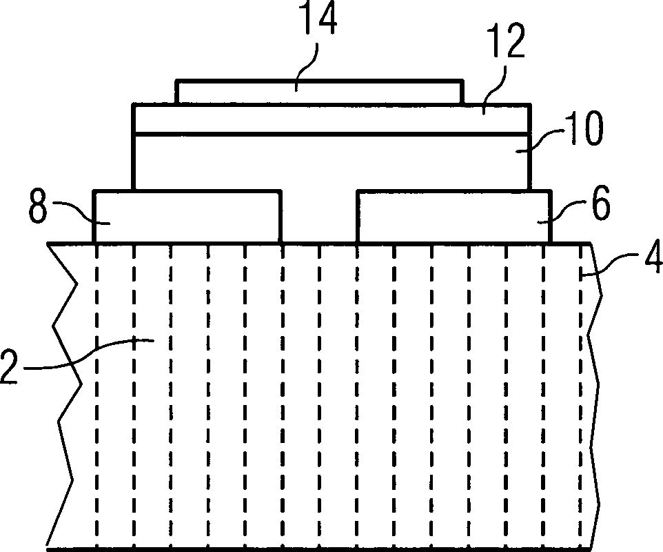
In
Auf
das geschrumpfte Substrat und die geschrumpften Elektroden
Es
können
auch komplette Schaltungen aus Polymerelektronik geschrumpft werden.
Es kann auch zuerst eine komplette Polymerelektronik-Schaltungsstruktur
wie beispielsweise in den
Das Schrumpfen kann auch durch vorheriges Ausdehnen eines elastischen Substrates erreicht werden. So kann beispielsweise ein elastisches Substrat (z. B. eine dünne PET-Folie, elastische Polymerfolie, ...) verwendet werden, das vor dem Strukturieren von Source/Drain-Elektrode gedehnt wird und anschließend von alleine schrumpft.The Shrinking can also be achieved by previously stretching an elastic Substrates can be achieved. For example, an elastic Substrate (eg a thin PET film, elastic polymer film, ...) can be used before the structuring of the source / drain electrode is stretched and then by alone shrinks.
Das Schrumpfen kann auch durch Entquellen eines vorher aufgequollenen Substrates erreicht werden. Das Substrat beispielsweise eine PET-Folie, eine Polymerfolie oder eine andere quellbare Folie kann in einem Bad (z. B. in einem Lösungsmittel) aufgequollen werden. Das Substrat kann auch gequollen hergestellt werden. Nach der Strukturierung von Source/Drain-Elektrode wird das Substrat durch Trocknen oder durch eine chemische Behandlung geschrumpft. Bei Verwendung eines gequollenen Substrats kann die organische Schaltung in allen drei Dimensionen geschrumpft werden. Wenn für die elektrischen Strukturen ebenfalls ein aufgequollenes leitendes oder halbleitendes Polymermaterial verwendet wird, können auch mehrschichtige elektrische Strukturen verwendet werden, ohne dass Scherspannungen zwischen dem Substrat und den elektrischen Strukturen auftreten können. Damit wird sich die elektrische Schaltung bzw. das Substrat beim Schrumpfen nicht verzeihen oder wölben.The Shrinking can also be done by draining a previously swollen Substrates can be achieved. The substrate, for example, a PET film, a Polymer film or other swellable film may be in a bath (eg in a solvent) be swollen. The substrate can also be made swollen become. After patterning of source / drain electrode becomes the substrate shrunk by drying or by a chemical treatment. When using a swollen substrate, the organic circuit shrunk in all three dimensions. If for the electrical Structures also a swollen conductive or semiconducting Polymer material used can also multilayer electrical Structures are used without shearing stresses between the substrate and the electrical structures can occur. In order to the electrical circuit or the substrate will shrink do not forgive or arch.
Es ist zu bemerken, dass das die geschrumpfte Schaltung nach dem Schrumpfen beispielsweise mit nicht schrumpffähigen Strukturen versehen werden kann.It It should be noted that this is the shrunken circuit after shrinking For example, be provided with non-shrinkable structures can.
Die vorliegende Erfindung beruht auf dem Schrumpfen strukturierter Schichten oder Schichtpaketen. Voraussetzung für den Schrumpfungsvorgang ist eine geeignete Wahl von Substrat und den sich darauf befindlichen Schichten. Wichtigste Eigenschaft des Substrates ist, dass es durch den Schrumpfungsvorgang maßstabsgerecht und reproduzierbar in einer, zwei oder drei Dimensionen verkleinert wird. Die sich in oder auf dem Substrat befindlichen Schichten müssen so gewählt sein, dass sie durch den Schrumpfungsvorgang nicht beschädigt werden. Der Schrumpfungsvorgang kann durch Einbringen von Energie, wie eine kurze thermische Behandlung wie z. B. Heizplatte, Heißluft-Fön, Bestrahlung, einen Ofen oder Eintauchen in ein heißes Bad erfolgen. Das Schrumpfen kann auch durch eine chemische Behandlung durch geeignete Chemikalien (je nach Substrat eine Säure, eine Lauge oder ein Lösungsmittel) erreicht werden.The The present invention is based on the shrinkage of structured layers or shift packages. Prerequisite for the shrinkage process is a suitable choice of substrate and those located thereon Layers. Most important property of the substrate is that it through the shrinking process to scale and reproducibly reduced in one, two or three dimensions becomes. The layers in or on the substrate must be chosen that they are not damaged by the shrinkage process. The shrinking process can be done by introducing energy, such as short thermal treatment such. Hot plate, hot air dryer, irradiation, an oven or immersion in a hot bath. The shrinking may also be due to a chemical treatment by suitable chemicals (depending on the substrate an acid, a caustic or a solvent) be achieved.
Ein Vorteil der Erfindung liegt in der prozesstechnisch einfachen Möglichkeit zur Verkleinerung des Source/Drain-Abstandes (d. h. der Kanallänge) beispielsweise von des OFETs und der damit verbundenen deutlichen Geschwindigkeitserhöhung der Polymerelektronikschaltung. Kombiniert man diese Verkleinerungsmethode mit Polymerelektronikschaltungen, welche durch Drucken hergestellt wurden, so kann man auf sehr kostengünstigen Weg schnelle integrierte Schaltungen produzieren. Ein weiterer Vorteil liegt in der Universalität der Methode: Es lassen sich damit auch lithografisch strukturierte Schichten verkleinern und somit auch extrem kleine und schnelle Polymerelektronikschaltungen erzeugen.One Advantage of the invention lies in the process technically simple way for reducing the source / drain distance (i.e., the channel length), for example of the OFET and the associated significant increase in speed of the Polymer electronics circuit. Combine this reduction method with polymer electronics circuits made by printing so you can quickly integrate in a very cost effective way Produce circuits. Another advantage lies in the universality of the method: It can thus be used to reduce lithographically structured layers and thus also extremely small and fast polymer electronics circuits produce.
Das verfahren ist auch bei einer Verbesserung der Drucktechniken weiterhin auch auf kleinere Ausgangsstrukturen anwendbar.The procedure is also in an improvement of printing techniques continue also applicable to smaller starting structures.
Für herkömmliche, auf Einkristallen basierende Materialsysteme der Mikroelektronik, wie z. B. Silizium oder Gallium-Arsenid lässt sich die vorliegende Erfindung prinzipiell nicht anwenden, da sich Einkristalle prinzipiell nicht verkleinern bzw. schrumpfen lassen.For conventional, Single-crystal based microelectronic material systems, such as As silicon or gallium arsenide, the present invention can be principally do not apply, as single crystals are not shrink or shrink.
Claims (10)
Priority Applications (1)
| Application Number | Priority Date | Filing Date | Title |
|---|---|---|---|
| DE10349027A DE10349027B4 (en) | 2003-10-22 | 2003-10-22 | Organic circuit with small structures and process for their preparation |
Applications Claiming Priority (1)
| Application Number | Priority Date | Filing Date | Title |
|---|---|---|---|
| DE10349027A DE10349027B4 (en) | 2003-10-22 | 2003-10-22 | Organic circuit with small structures and process for their preparation |
Publications (2)
| Publication Number | Publication Date |
|---|---|
| DE10349027A1 DE10349027A1 (en) | 2005-06-02 |
| DE10349027B4 true DE10349027B4 (en) | 2006-06-22 |
Family
ID=34529702
Family Applications (1)
| Application Number | Title | Priority Date | Filing Date |
|---|---|---|---|
| DE10349027A Expired - Fee Related DE10349027B4 (en) | 2003-10-22 | 2003-10-22 | Organic circuit with small structures and process for their preparation |
Country Status (1)
| Country | Link |
|---|---|
| DE (1) | DE10349027B4 (en) |
Cited By (3)
| Publication number | Priority date | Publication date | Assignee | Title |
|---|---|---|---|---|
| DE102008061928A1 (en) | 2008-12-15 | 2010-06-17 | Polylc Gmbh & Co. Kg | Organic electronic circuit |
| DE102009012302A1 (en) | 2009-03-11 | 2010-09-23 | Polyic Gmbh & Co. Kg | Organic electronic component i.e. parallel-series converter, for converting parallel input signal of N bit into serial output signal, has output electrically connected with electrode that is arranged on surface of semiconductor layer |
| US8056815B2 (en) | 2007-09-27 | 2011-11-15 | Polyic Gmbh & Co. Kg | RFID transponder |
Citations (1)
| Publication number | Priority date | Publication date | Assignee | Title |
|---|---|---|---|---|
| EP0793900B1 (en) * | 1994-07-19 | 2001-10-04 | Forskarpatent i Linköping AB | Fabrication of an electroluminescent device |
-
2003
- 2003-10-22 DE DE10349027A patent/DE10349027B4/en not_active Expired - Fee Related
Patent Citations (1)
| Publication number | Priority date | Publication date | Assignee | Title |
|---|---|---|---|---|
| EP0793900B1 (en) * | 1994-07-19 | 2001-10-04 | Forskarpatent i Linköping AB | Fabrication of an electroluminescent device |
Non-Patent Citations (2)
| Title |
|---|
| Fix,W. et al: "Fast polymer integrated Circuits". In: Appl. Phys. Lett., Vol. 81, No. 9, Aug. 2002, pp. 1735-1737 * |
| Gelinck,G.H. et al: "High performance all-polymer integrated Circuits". In: Appl. Phys. Lett., Vol.77, No. 10, 4 Sept. 2000, pp. 1487-1489 * |
Cited By (4)
| Publication number | Priority date | Publication date | Assignee | Title |
|---|---|---|---|---|
| US8056815B2 (en) | 2007-09-27 | 2011-11-15 | Polyic Gmbh & Co. Kg | RFID transponder |
| DE102008061928A1 (en) | 2008-12-15 | 2010-06-17 | Polylc Gmbh & Co. Kg | Organic electronic circuit |
| WO2010075953A1 (en) | 2008-12-15 | 2010-07-08 | Polyic Gmbh & Co. Kg | Organic electronic circuit |
| DE102009012302A1 (en) | 2009-03-11 | 2010-09-23 | Polyic Gmbh & Co. Kg | Organic electronic component i.e. parallel-series converter, for converting parallel input signal of N bit into serial output signal, has output electrically connected with electrode that is arranged on surface of semiconductor layer |
Also Published As
| Publication number | Publication date |
|---|---|
| DE10349027A1 (en) | 2005-06-02 |
Similar Documents
| Publication | Publication Date | Title |
|---|---|---|
| DE10126860C2 (en) | Organic field effect transistor, process for its manufacture and use for the construction of integrated circuits | |
| EP1316116B1 (en) | Method for structuring an organic field effect transistor | |
| EP1559147B1 (en) | Film comprising organic semiconductors | |
| EP1346422A1 (en) | Organic field-effect transistor, method for structuring an ofet and integrated circuit | |
| EP1289031A2 (en) | Method of manufactoring a structured conducting polymer layer | |
| EP1676330A2 (en) | Structuring of electrical functional layers by means of a transfer film and structuring the adhesive | |
| EP2387076A1 (en) | Field effect transistor and electric circuit | |
| DE10153562A1 (en) | Process for reducing the electrical contact resistance in organic field-effect transistors by embedding nanoparticles to produce field peaks at the interface between the contact material and the organic semiconductor material | |
| WO2005020257A2 (en) | Organic capacitor having a voltage-controlled capacitance | |
| DE102009001919B4 (en) | A method of manufacturing a plurality of integrated semiconductor devices | |
| DE10349027B4 (en) | Organic circuit with small structures and process for their preparation | |
| EP1699637B1 (en) | Method for further printing with electrical conductivity | |
| DE102011004543B4 (en) | Resistor, circuit board and electrical or electronic device | |
| DE102007030308A1 (en) | Method for producing a memory structure | |
| EP1911108B1 (en) | Method for producing an electronic component | |
| EP1704606B1 (en) | Method for the production of an organic transistor comprising a self-adjusting gate electrode | |
| EP1925033A1 (en) | Electronic circuit and method for the manufacture of the same | |
| DE102006027292B4 (en) | Process for producing a structured layer sequence on a substrate | |
| DE10120685C1 (en) | Encapsulated organic-electronic circuit has electronic components especially made of organic material and arranged between at least two layers forming barrier | |
| EP1922774B1 (en) | Organic component and electric circuit comprising said component | |
| WO2005006462A1 (en) | Method and device for structuring organic layers | |
| EP2154724A2 (en) | Flexible flat structure with a layer having microstructures, method for producing the flexible flat structure and use thereof | |
| DE10356675A1 (en) | Production of an electrode arrangement for a field effect transistor comprises forming an electrically conducting film, dividing along a separating line forming a gap, and extending electrodes against each other | |
| EP2027615A1 (en) | Component with a structured layer on a carrier substrate | |
| WO2008012080A1 (en) | Method for producing at least one component and component |
Legal Events
| Date | Code | Title | Description |
|---|---|---|---|
| OP8 | Request for examination as to paragraph 44 patent law | ||
| 8127 | New person/name/address of the applicant |
Owner name: POLYIC GMBH & CO. KG, 91052 ERLANGEN, DE |
|
| 8327 | Change in the person/name/address of the patent owner |
Owner name: POLYIC GMBH & CO. KG, 91052 ERLANGEN, DE |
|
| 8364 | No opposition during term of opposition | ||
| 8327 | Change in the person/name/address of the patent owner |
Owner name: POLYIC GMBH & CO.KG, 90763 FUERTH, DE |
|
| R119 | Application deemed withdrawn, or ip right lapsed, due to non-payment of renewal fee |