DE102007003282A1 - LED chip - Google Patents
LED chip Download PDFInfo
- Publication number
- DE102007003282A1 DE102007003282A1 DE102007003282A DE102007003282A DE102007003282A1 DE 102007003282 A1 DE102007003282 A1 DE 102007003282A1 DE 102007003282 A DE102007003282 A DE 102007003282A DE 102007003282 A DE102007003282 A DE 102007003282A DE 102007003282 A1 DE102007003282 A1 DE 102007003282A1
- Authority
- DE
- Germany
- Prior art keywords
- layer
- type
- chip according
- led chip
- layers
- Prior art date
- Legal status (The legal status is an assumption and is not a legal conclusion. Google has not performed a legal analysis and makes no representation as to the accuracy of the status listed.)
- Granted
Links
Classifications
-
- H—ELECTRICITY
- H10—SEMICONDUCTOR DEVICES; ELECTRIC SOLID-STATE DEVICES NOT OTHERWISE PROVIDED FOR
- H10H—INORGANIC LIGHT-EMITTING SEMICONDUCTOR DEVICES HAVING POTENTIAL BARRIERS
- H10H20/00—Individual inorganic light-emitting semiconductor devices having potential barriers, e.g. light-emitting diodes [LED]
- H10H20/80—Constructional details
- H10H20/83—Electrodes
- H10H20/831—Electrodes characterised by their shape
- H10H20/8312—Electrodes characterised by their shape extending at least partially through the bodies
-
- H—ELECTRICITY
- H10—SEMICONDUCTOR DEVICES; ELECTRIC SOLID-STATE DEVICES NOT OTHERWISE PROVIDED FOR
- H10H—INORGANIC LIGHT-EMITTING SEMICONDUCTOR DEVICES HAVING POTENTIAL BARRIERS
- H10H20/00—Individual inorganic light-emitting semiconductor devices having potential barriers, e.g. light-emitting diodes [LED]
- H10H20/80—Constructional details
- H10H20/81—Bodies
- H10H20/816—Bodies having carrier transport control structures, e.g. highly-doped semiconductor layers or current-blocking structures
- H10H20/8162—Current-blocking structures
-
- H—ELECTRICITY
- H10—SEMICONDUCTOR DEVICES; ELECTRIC SOLID-STATE DEVICES NOT OTHERWISE PROVIDED FOR
- H10H—INORGANIC LIGHT-EMITTING SEMICONDUCTOR DEVICES HAVING POTENTIAL BARRIERS
- H10H20/00—Individual inorganic light-emitting semiconductor devices having potential barriers, e.g. light-emitting diodes [LED]
- H10H20/80—Constructional details
- H10H20/83—Electrodes
- H10H20/832—Electrodes characterised by their material
- H10H20/835—Reflective materials
-
- H—ELECTRICITY
- H10—SEMICONDUCTOR DEVICES; ELECTRIC SOLID-STATE DEVICES NOT OTHERWISE PROVIDED FOR
- H10H—INORGANIC LIGHT-EMITTING SEMICONDUCTOR DEVICES HAVING POTENTIAL BARRIERS
- H10H20/00—Individual inorganic light-emitting semiconductor devices having potential barriers, e.g. light-emitting diodes [LED]
- H10H20/80—Constructional details
- H10H20/81—Bodies
- H10H20/819—Bodies characterised by their shape, e.g. curved or truncated substrates
- H10H20/82—Roughened surfaces, e.g. at the interface between epitaxial layers
-
- H—ELECTRICITY
- H10—SEMICONDUCTOR DEVICES; ELECTRIC SOLID-STATE DEVICES NOT OTHERWISE PROVIDED FOR
- H10H—INORGANIC LIGHT-EMITTING SEMICONDUCTOR DEVICES HAVING POTENTIAL BARRIERS
- H10H20/00—Individual inorganic light-emitting semiconductor devices having potential barriers, e.g. light-emitting diodes [LED]
- H10H20/80—Constructional details
- H10H20/84—Coatings, e.g. passivation layers or antireflective coatings
Landscapes
- Led Devices (AREA)
Abstract
Es wird ein Leuchtdiodenchip mit einer Schichtenfolge (10) angegeben, die mindestens eine n-leitende Schicht aufweist. Der Leuchtdiodenchip weist eine leitend mit der n-leitenden Schicht verbundene Spiegelschicht auf. Zwischen der n-leitenden Schicht und der Spiegelschicht ist mindestens eine transparente dielektrische Schicht angeordnet.It a light-emitting diode chip with a layer sequence (10) is given, having at least one n-type layer. The LED chip has a mirror layer conductively connected to the n-type layer on. Between the n-type layer and the mirror layer is at least one transparent dielectric layer is arranged.
Description
Es wird ein Leuchtdiodenchip, d. h. ein optoelektronischer Halbleiterchip, angegeben.It a light-emitting diode chip, i. H. an optoelectronic semiconductor chip, specified.
Eine zu lösende Aufgabe besteht darin, einen Leuchtdiodenchip mit hoher Strahlungseffizienz anzugeben, der niedrige Verluste aufweist.A to be solved The object is to specify a light-emitting diode chip with high radiation efficiency, which has low losses.
Gemäß einer ersten bevorzugten Ausführungsform wird ein Leuchtdiodenchip mit einer Schichtenfolge angegeben, die mindestens eine n-leitende Schicht aufweist. Der Leuchtdiodenchip umfasst einen Spiegel, der mit der Schichtenfolge fest verbunden ist. Der Spiegel weist eine leitend mit der n-leitenden Schicht verbundene, elektrisch leitende Spiegelschicht auf. Der Spiegel umfasst ferner mindestens eine dielektrische Schicht, die zwischen der n-leitenden Schicht und der elektrisch leitenden Spiegelschicht angeordnet ist. Die dielektrische Schicht ist vorzugsweise transparent.According to one first preferred embodiment a light-emitting diode chip is specified with a layer sequence, the has at least one n-type layer. The LED chip comprises a mirror that is firmly connected to the layer sequence. Of the Mirror has a conductive connected to the n-type layer, electrically conductive mirror layer. The mirror further comprises at least a dielectric layer interposed between the n-type layer and the electrically conductive mirror layer is arranged. The Dielectric layer is preferably transparent.
Der Brechungsindex der dielektrischen Schicht ist kleiner als derjenige der an die dielektrische Schicht angrenzenden Schicht der Schichtenfolge. Durch die Verwendung der dielektrischen Schicht mit einem kleinen Brechungsindex können die auf die dielektrische Schicht flach einfallenden Strahlungskomponenten vollständig reflektiert werden. Somit ist es sogar möglich, eine Ag-freie Spiegelschicht einzusetzen. Ein silberfreier Spiegel enthält beispielsweise Al, Rh, Rt. Somit gelingt es, die Feuchtestabilität sowie die Langzeitstabilität des Chips zu erhöhen.Of the Refractive index of the dielectric layer is smaller than that the layer of the layer sequence adjoining the dielectric layer. By using the dielectric layer with a small Refractive index can the on the dielectric layer flat incident radiation components Completely be reflected. Thus, it is even possible to use an Ag-free mirror layer use. A silver-free mirror contains, for example, Al, Rh, Rt. Thus, it succeeds, the moisture stability and the long-term stability of the chip to increase.
Die mindestens eine dielektrische Schicht weist in einer Variante mindestens zwei übereinander angeordnete Schichten mit unterschiedlich großen Brechungsindizes auf, die zusammen einen Bragg-Spiegel bilden. Bei mehr als zwei dielektrischen Schichten sind die Schichten mit einer relativ hohen und einer relativ niedrigen Brechzahl in abwechselnder Reihenfolge angeordnet. Die Dicke der jeweiligen Schicht beträgt vorzugsweise eine Viertelwellenlänge der in der aktiven Zone erzeugten Strahlung. Das Verhältnis der Brechzahlen der aufeinander folgenden Schichten beträgt vorzugsweise mindestens 1,25.The at least one dielectric layer has at least one variant two superimposed Layers with different refractive indices, the together form a Bragg mirror. For more than two dielectric Layers are the layers with a relatively high and a relative low refractive index arranged in alternating order. The Thickness of the respective layer is preferably a quarter wavelength of the radiation generated in the active zone. The ratio of Refractive indices of the successive layers is preferably at least 1.25.
Der Spiegel kann alternativ eine Abfolge von dielektrischen und elektrisch leitenden Schichten aufweisen, wobei die Schichten mit einer relativ hohen und einer relativ niedrigen Brechzahl in abwechselnder Reihenfolge angeordnet sind.Of the Mirror may alternatively be a sequence of dielectric and electrical conductive layers, wherein the layers with a relative high and a relatively low refractive index in alternating order are arranged.
Bei der Variante mit dem Bragg-Spiegel ist es möglich, eine elektrisch leitende Spiegelschicht zu verwenden, deren Reflektivität nicht besonders hoch ist, wobei sie z. B. 95% nicht übersteigt.at The variant with the Bragg mirror makes it possible to have an electrically conductive Mirror layer whose reflectivity is not particularly high, where they are z. B. 95% does not exceed.
Die jeweilige n-leitende Schicht der Schichtenfolge kann durch die dielektrische Schicht oder die dielektrischen Schichten des Bragg-Spiegels hindurch z. B. über vertikale elektrische Verbindungen kontaktiert werden. Die vertikalen elektrischen Verbindungen werden nachstehend als Durchkontaktierungen bezeichnet.The The respective n-type layer of the layer sequence may be formed by the dielectric Layer or the dielectric layers of the Bragg mirror through z. B. over vertical electrical connections are contacted. The vertical electrical connections are hereinafter referred to as vias designated.
Besonders vorteilhaft ist eine Variante der Schichtenfolge mit einer ersten und einer zweiten n-leitenden Schicht. Die Schichtenfolge weist eine p-leitende Schicht auf, die zwischen den beiden n-leitenden Schichten angeordnet ist (npn-Schichtaufbau). Die n-leitenden Schichten sind vorzugsweise die endständigen Schichten der Schichtenfolge. Zumindest ist die aktive Zone und die p-leitende Schicht zwischen den beiden n-leitenden Schichten angeordnet.Especially a variant of the layer sequence with a first is advantageous and a second n-type layer. The layer sequence points a p-type layer between, the two n-type Layers is arranged (npn layer structure). The n-type layers are preferably the terminal layers the sequence of layers. At least the active zone and the p-type Layer disposed between the two n-type layers.
Die erste n-leitende Schicht ist eine an die strahlungserzeugende aktive Zone angrenzende Schicht. Die zweite n-leitende Schicht bildet einen Tunnelkontakt mit der p-leitenden Schicht der Schichtenfolge. Die erste und zweite n-leitende Schicht können in allen Ausführungsbeispielen gegeneinander ausgetauscht werden. Dies bedeutet, dass die Reihenfolge der Schichten der Schichtenfolge bei fixer Lage des Spiegels umgedreht werden kann.The first n-type layer is one active to the radiation-generating Zone adjacent layer. The second n-type layer forms a tunnel junction with the p-type layer of the layer sequence. The first and second n-conductive layer can in all embodiments be exchanged for each other. This means that the order the layers of the layer sequence turned over at a fixed position of the mirror can be.
Der Spiegel ist entweder mit der ersten oder mit der zweiten n-leitenden Schicht leitend verbunden. Die dielektrische Schicht ist in einer Variante zwischen der ersten n-leitenden Schicht und der Spiegelschicht angeordnet. Die dielektrische Schicht ist in einer weiteren Variante zwischen der zweiten n-leitenden Schicht und der Spiegelschicht angeordnet.Of the Mirror is either the first or the second n-type Layer conductively connected. The dielectric layer is in one Variant between the first n-type layer and the mirror layer arranged. The dielectric layer is in a further variant between the second n-type layer and the mirror layer arranged.
Mindestens eine der n-leitenden Schichten wird als eine Kontaktschicht benutzt. Als Kontaktschicht wird eine Schicht bezeichnet, die durch einen Anschlussdraht kontaktiert wird, der an eine Stromquelle angeschlossen ist. In einer Variante werden beide n-leitenden Schichten als jeweils eine Kontaktschicht benutzt. Alternativ kann eine der n-leitenden Schichten als eine erste Kontaktschicht und die Spiegelschicht als eine zweite Kontaktschicht benutzt werden.At least one of the n-type layers is used as a contact layer. As a contact layer, a layer is referred to, through a connecting wire contacted, which is connected to a power source. In In one variant, both n-type layers are each one Contact layer used. Alternatively, one of the n-type layers as a first contact layer and the mirror layer as a second Contact layer can be used.
Gemäß einer zweiten bevorzugten Ausführungsform wird ein Leuchtdiodenchip mit einer Schichtenfolge angegeben, die in einer Wachstumsrichtung in der angegebenen Reihenfolge aufeinander folgende Schichten aufweist: eine erste n-leitende Schicht, eine strahlungserzeugende aktive Zone, eine gleitende Schicht und eine zweite n-leitende Schicht. Zwischen der p-leitenden Schicht und der zweiten n-leitenden Schicht ist ein Tunnelkontakt gebildet.According to one second preferred embodiment a light-emitting diode chip is specified with a layer sequence, the in a growth direction in the order given to each other comprising: a first n-type layer, a radiation-generating active zone, a sliding layer and a second n-type layer. Between the p-type layer and the second n-type layer is formed a tunnel junction.
Die zweite n-leitende Schicht dient als eine Stromaufweitungsschicht, die an eine Stromquelle angeschlossen wird. Durch die Einführung der Stromaufweitungsschicht kann der Spiegel vom elektrischen Kontakt entkoppelt werden. Dadurch wird es zum einen ermöglicht, einen hochreflektierenden Spiegel mit einer dielektrischen Schicht zu verwenden, und zum anderen kann der Kontaktwiderstand beim Kontaktieren der Schichtenfolge in hohem Maße reduziert werden. Somit kann die Gesamteffizienz des Leuchtdiodenchips deutlich erhöht werden.The second n-type layer serves as a current spreading layer, which is connected to a power source. By introducing the current spreading layer The mirror can be decoupled from electrical contact. Thereby is it possible, on the one hand, a highly reflective mirror with a dielectric layer on the other hand, the contact resistance when contacting the layer sequence to a large extent be reduced. Thus, the overall efficiency of the LED chip clearly increased become.
Gemäß einer dritten bevorzugten Ausführungsform wird ein Leuchtdiodenchip mit einer Schichtenfolge angegeben, die zwei Schichten des gleichen Leitfähigkeitstyps aufweist, zwischen denen eine strahlungserzeugende aktive Zone angeordnet ist.According to one third preferred embodiment a light-emitting diode chip is specified with a layer sequence, the two layers of the same conductivity type, between where a radiation-generating active zone is arranged.
Die zwei Schichten des gleichen Leitfähigkeitstyps weisen eine erste Schicht und eine zweite Schicht des ersten Leitfähigkeitstyps auf, wobei die vorzugsweise relativ dünne zweite Schicht des ersten Leitfähigkeitstyps als ein Ladungsträger-Reservoir zur Erhöhung der Ladungsträgerkonzentration des ersten Leitfähigkeitstyps in der Nähe der aktiven Zone vorgesehen ist. Die Schichtenfolge weist eine Schicht des zweiten Leitfähigkeitstyps auf, die an die zweite Schicht des ersten Leitfähigkeitstyps angrenzt. Der erste Leitfähigkeitstyp ist n-Typ und der zweite Leitfähigkeitstyp p-Typ, oder umgekehrt.The two layers of the same conductivity type have a first one Layer and a second layer of the first conductivity type, wherein preferably relatively thin second layer of the first conductivity type as a charge carrier reservoir for increasing the Charge carrier concentration of first conductivity type near the active zone is provided. The layer sequence has a layer of the second conductivity type which adjoins the second layer of the first conductivity type. Of the first conductivity type is n-type and the second conductivity type p-type, or vice versa.
Die Schichtenfolge weist in einer Variante eine weitere Schichte des zweiten Leitfähigkeitstyps auf, die mit der ers ten Schicht des ersten Leitfähigkeitstyps einen Tunnelkontakt bildet.The Layer sequence has in a variant another layer of the second conductivity type, the tunnel contact with the first layer of the first conductivity type forms.
Die Wachstumsrichtung bei der Erzeugung der Schichtenfolge kann im Prinzip beliebig sein.The Growth direction in the generation of the layer sequence can in principle be arbitrary.
Die Dicke der zweiten Schicht des ersten Leitfähigkeitstyps ist vorzugsweise kleiner als diejenige der ersten Schicht. Die Dicke der zweiten Schicht beträgt vorzugsweise maximal 20% derjenigen der ersten Schicht. Die zweite Schicht des ersten Leitfähigkeitstyps ist vorzugsweise maximal 20 nm dick.The Thickness of the second layer of the first conductivity type is preferable smaller than that of the first layer. The thickness of the second Layer is preferably at most 20% of that of the first layer. The second Layer of the first conductivity type is preferably at most 20 nm thick.
In einer vorteilhaften Variante weist die Schichtenfolge die in der angegebenen Reihenfolge aufeinander folgende Schichten auf: eine p-leitende erste Schicht, eine strahlungserzeugende aktive Zone, eine weitere p-leitende zweite Schicht, die als Löcherreservoir dient, und eine n-leitende Schicht.In an advantageous variant, the layer sequence in the specified sequence successive layers: one p-type first layer, a radiation-generating active zone, another p-type second layer acting as a hole reservoir serves, and an n-type layer.
Die beiden p-leitenden Schichten bilden eine p-leitende Zone. Die aktive Zone ist in dieser Variante nicht an einem pn-Übergang, sondern in der Nähe des pn-Übergangs innerhalb der p-leitenden Zone angeordnet. Das Verlagern der aktiven Zone von der Grenzfläche des pn-Übergangs in die Zone mit einem bestimmten Leitfähigkeitstyp, in diesem Fall p-Typ, erhöht die Effizienz bei der Strahlungserzeugung.The Both p-type layers form a p-type zone. The active one Zone is not at a pn junction in this variant, but near the pn junction arranged within the p-type zone. Shifting the active Zone from the interface of the pn junction into the zone with a certain conductivity type, in this case p-type, increased the efficiency of radiation generation.
In einer weiteren vorteilhaften Variante weist die Schichtenfolge die in der angegebenen Reihenfolge aufeinander folgende Schichten auf: eine n-leitende erste Schicht, eine strahlungserzeugende aktive Zone, eine n-leitende zweite Schicht, die als Elektronenreservoir dient, und eine p-leitende Schicht.In In a further advantageous variant, the layer sequence has the consecutive layers in the order given: an n-type first layer, a radiation-generating active Zone, an n-type second layer acting as an electron reservoir serves, and a p-type layer.
Die beiden n-leitenden Schichten bilden eine n-leitende Zone. Die aktive Zone ist in dieser Variante nicht an einem pn-Übergang, sondern in der Nähe des pn-Übergangs innerhalb der n-leitenden Zone angeordnet.The Both n-type layers form an n-type region. The active one Zone is not at a pn junction in this variant, but near the pn junction arranged within the n-type zone.
Gemäß einer vierten bevorzugten Ausführungsform wird ein Leuchtdiodenchip angegeben mit einer Schichtenfolge, die folgende Schichten aufweist: zwei n-leitende Schichten, eine strahlungserzeugende aktive Zone und eine p-leitende Schicht. Auf der in Auskopplungsrichtung obersten der n-leitenden Schichten ist eine Anschlussfläche angeordnet. In der Schichtenfolge ist zumindest unterhalb der Anschlussfläche eine Aussparung ausgebildet, die sich in Auskopplungsrichtung zumindest bis zur obersten der n-leitenden Schichten erstreckt. Die Aussparung ist zumindest im Bereich ihrer Mantelflächen durch ein dielektrisches Material ausgekleidet. Der Boden der Aussparung ist in Vertikalrichtung von der Anschlussfläche beabstandet.According to one fourth preferred embodiment a light-emitting diode chip is specified with a layer sequence, the comprising the following layers: two n-type layers, one radiation-generating layer active zone and a p-type layer. On the in decoupling direction top of the n-type layers, a pad is arranged. In the layer sequence is at least below the pad a Recess formed, which in the extraction direction at least extends to the top of the n-type layers. The recess is at least in the region of its lateral surfaces by a dielectric Material lined. The bottom of the recess is in the vertical direction from the connection surface spaced.
In der Aussparung ist in einer Variante eine Durchkontaktierung zur elektrischen Kontaktierung der in Auskopplungsrichtung obersten der n-leitenden Schichten angeordnet.In the recess is in a variant of a via for electrical contacting of the top in the outfeed direction arranged the n-type layers.
Die Schichtenfolge ist vorzugsweise mit einem Spiegel fest verbunden, der zumindest eine elektrisch leitfähige Spiegelschicht aufweist, die vorzugsweise mit einer der n-leitenden Schichten der Schichtenfolge elektrisch verbunden ist. Der Spiegel kann darüber hinaus eine transparente dielektrische Schicht umfassen, die zwischen der Spiegelschicht und der Schichtenfolge angeordnet ist.The Layer sequence is preferably firmly connected to a mirror, which has at least one electrically conductive mirror layer, preferably with one of the n-type layers of the layer sequence electrically connected. The mirror can also be transparent dielectric layer between the mirror layer and the layer sequence is arranged.
In der dielektrischen Schicht ist in einer Variante eine Durchkontaktierung zur elektrischen Kontaktierung der in Auskopplungsrichtung untersten der n-leitenden Schichten angeordnet.In the dielectric layer is in one variant a via for electrical contacting of the lowermost in Auskopplungsrichtung arranged the n-type layers.
Die angegebenen Ausführungsformen sind beliebig miteinander kombinierbar.The specified embodiments can be combined with each other.
Nachstehend werden vorteilhafte Ausgestaltungen des Leuchtdiodenchips erläutert.below Advantageous embodiments of the LED chip will be explained.
Der Leitfähigkeitstyp der Schichten der Schichtenfolge kann z. B. n-Typ oder p-Typ sein. In einer Halbleiterschicht mit der Leitfähigkeit des n-Typs sind die Elektronen und in einer Halbleiterschicht mit der Leitfähigkeit des p-Typs die Löcher die Majoritätsladungsträger.The conductivity type of the layers of the layer sequence can, for. B. n-type or p-type. In a semiconductor layer with the conductivity of the n-type are the electrons, and in a p-type conductivity semiconductor layer, the holes are majority carriers.
Die Schichten mit der Leitfähigkeit des n-Typs werden als n-leitende Schichten und die Schichten mit der Leitfähigkeit des p-Typs als p-leitende Schichten bezeichnet.The Layers of conductivity of the n-type are called n-type Layers and the p-type conductivity layers as p-type Called layers.
Die Schichtenfolge umfasst eine p-leitende Schicht und eine strahlungserzeugende aktive Zone, die zwischen der p-leitenden Schicht und der ersten n-leitenden Schicht angeordnet.The Layer sequence comprises a p-type layer and a radiation-generating layer active zone, between the p-type layer and the first n-type Layer arranged.
Die Schichten der Schichtenfolge sind vorzugsweise epitaktisch aufgewachsen. Die Schichtenfolge ist beispielsweise auf der Basis von GaN gebildet. Die aktive Zone ist in einer Variante durch eine Schicht gebildet, die InGaN oder InGaAlN enthält. Der In-Gehalt beträgt vorzugsweise bis 50%. Der genaue Spektralbereich der in der aktiven Zone erzeugten Strahlung hängt vom In-Gehalt ab und kann im Prinzip beliebig sein. Zur Erzeugung eines Weißlichtes kann auf der Auskoppel seite ein Converter vorgesehen sein.The Layers of the layer sequence are preferably grown epitaxially. The layer sequence is formed, for example, on the basis of GaN. The active zone is formed in a variant by a layer, containing InGaN or InGaAlN. Of the In content is preferably up to 50%. The exact spectral range of the active Zone generated radiation hangs from the In content and may in principle be arbitrary. To produce a white light can be provided on the Auskoppel page a converter.
Die Schichtenfolge weist in einer vorteilhaften Variante eine p-leitende Schicht, eine weitere p-leitende Schicht und eine zwischen den p-leitenden Schichten angeordnete strahlungserzeugende aktive Zone auf. Die weitere p-leitende Schicht ist zwischen der aktiven Zone und der ersten n-leitenden Schicht angeordnet. Die Dicke der weiteren p-leitenden Schicht beträgt beispielsweise 0,1 nm bis 100 nm, in einer Variante 0,1 nm bis 10 nm. Der Mindestwert für Dotierung bei der weiteren p-leitenden Schicht beträgt vorzugsweise 1018 Mg-Atome pro cm3.In an advantageous variant, the layer sequence has a p-type layer, a further p-type layer and a radiation-generating active zone arranged between the p-type layers. The further p-type layer is arranged between the active zone and the first n-type layer. The thickness of the further p-type layer is, for example, 0.1 nm to 100 nm, in one variant 0.1 nm to 10 nm. The minimum value for doping in the other p-type layer is preferably 10 18 Mg atoms per cm 3 ,
Die Schichtenfolge umfasst in einer bevorzugten Variante eine zweite n-leitende Schicht. Die p-leitende Schicht ist vorzugsweise zwischen der zweiten n-leitenden Schicht und der aktiven Zone angeordnet. Zwischen der p-leitenden Schicht und der zweiten n-leitenden Schicht ist ein Tunnelkontakt gebildet.The Layer sequence comprises in a preferred variant a second one n-type layer. The p-type layer is preferably between the second n-type layer and the active region. Between the p-type layer and the second n-type layer a tunnel contact is formed.
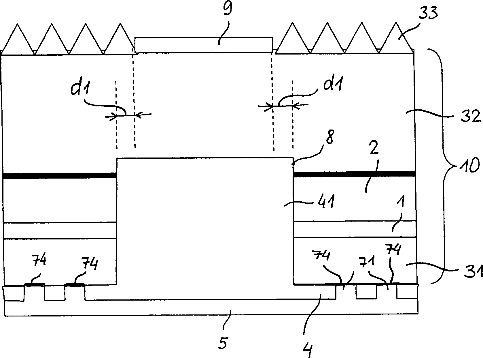
Die Spiegelschicht ist mit der ersten n-leitenden Schicht über mindestens eine erste Durchkontaktierung, in einer vorteilhaften Variante über mehrere Durchkontaktierungen, die in der dielektrischen Schicht angeordnet sind, leitend verbunden.The Mirror layer is at least with the first n-type layer a first via, in an advantageous variant over several Vias disposed in the dielectric layer are connected, conducting.
Mit mehreren Durchkontaktierungen gelingt es, den Kontaktwiderstand zu reduzieren und somit den Potentialunterschied zwischen der Spiegelschicht und der leitend mit ihr verbundenen n-leitenden Schicht gegenüber der Variante mit nur einer Durchkontaktierung zu verringern. An der Grenzfläche der jeweiligen ersten Durchkontaktierung und der n-leitenden Schicht ist ein vorzugsweise niederohmiger elektrischer Kon takt gebildet. Die Gesamtfläche dieser Kontakte beträgt vorzugsweise maximal 10%, in einer vorteilhaften Variante maximal 5% der Grundfläche der Schichtenfolge.With several vias succeeds, the contact resistance to reduce and thus the potential difference between the mirror layer and the n-type layer conductively connected thereto To reduce variant with only one via. At the interface the respective first via and the n-type layer is a preferably low-impedance electrical con tact formed. The total area of these contacts is preferably at most 10%, in an advantageous variant maximum 5% of the floor area the sequence of layers.
Der laterale Abstand zwischen den ersten Durchkontaktierungen beträgt vorzugsweise 20–30 Mikrometer, was gegenüber der Dicke der dielektrischen Schicht, die beispielsweise 10 bis 2000 nm, in einer bevorzugten Variante 400–600 nm beträgt, relativ groß ist.Of the lateral distance between the first vias is preferably 20-30 microns, what about the thickness of the dielectric layer, for example, 10 to 2000 nm, in a preferred variant 400-600 nm, relative is great.
Die dielektrische Schicht wirkt für Strahlungskomponenten, die einen relativ flachen Einfallswinkel – beispielsweise über 30° – aufweisen, als ein nahezu perfekter Spiegel, dessen Reflexionskoeffizient annähernd 100% beträgt (Totalreflexion). Da bei der Totalreflexion an der dielektrischen Schicht keine Absorption stattfindet, können Absorptionsverluste für die flachen Einfallswinkel praktisch ausgeschlossen werden.The Dielectric layer acts for Radiation components having a relatively shallow angle of incidence - for example, over 30 ° -, as a nearly perfect mirror whose reflection coefficient is approximately 100% is (Total reflection). As in total reflection at the dielectric Layer no absorption takes place, absorption losses for the shallow Incidence angles are practically excluded.
Die dielektrische Schicht ist für die in der aktiven Zone erzeugte Strahlung vorzugsweise transparent. Die Strahlungskomponenten, die im Wesentlichen senkrecht auf die Grenzfläche der dielektrischen Schicht und der an diese angrenzenden n-leitenden einfallen, werden im Wesentlichen nicht an dieser Grenzfläche, sondern an der Grenzfläche der dielektrischen Schicht und der Spiegelschicht reflektiert.The Dielectric layer is for the radiation generated in the active zone is preferably transparent. The radiation components, which are essentially perpendicular to the interface the dielectric layer and the adjacent n-type conductive, are essentially not at this interface, but at the interface of the dielectric Layer and the mirror layer reflected.
Der Brechungsindex der dielektrischen Schicht ist vorzugsweise um mindestens einen Faktor 1,5 kleiner als derjenige der zu ihr gewandten Schicht der Schichtenfolge, z. B. der ersten oder zweiten n-leitenden Schicht. Als Materialien für die dielektrische Schicht kommen insbesondere Siliziumdioxid, Siliziumnitrid und Spin-On Glas in Betracht. Weitere transparente, in einer Variante poröse, dielektrische Materialien, deren Brechungsindex kleiner als 1,5 ist, sind auch geeignet. Vorteilhaft sind transparente poröse Materialien, deren Brechungsindex annähernd demjenigen der Luft gleich ist.Of the Refractive index of the dielectric layer is preferably at least about a factor of 1.5 smaller than that of the layer facing it the layer sequence, z. B. the first or second n-type layer. As materials for the dielectric layer is in particular silicon dioxide, silicon nitride and spin-on glass into consideration. Further transparent, in a variant porous dielectric materials whose refractive index is less than 1.5 is, are also suitable. Advantageous are transparent porous materials, their refractive index approximate the same as the air.
Der Gewinn an Auskoppeleffizienz durch die Verwendung der dielektrischen Schicht mit der Brechzahl 1,5 beträgt mindestens 10% gegenüber der Variante mit einem Spiegel, der nur Metallschichten, d. h. keine dielektrische Schicht, aufweist.Of the Gain in extraction efficiency through the use of the dielectric Layer with the refractive index 1.5 is at least 10% over the Variant with a mirror that only metal layers, d. H. none dielectric layer.
Die Spiegelschicht enthält vorzugsweise Metall, z. B. Al, Ag, PtAg und/oder andere geeignete Metalle oder Metalllegierungen, inklusive deren Kombination. Die Dicke der Pt-Schicht bei PtAg beträgt vorzugsweise maximal 3 nm, in einer vorteilhaften Variante maximal 0,3 nm.The Mirror layer contains preferably metal, e.g. As Al, Ag, PtAg and / or other suitable Metals or metal alloys, including their combination. The Thickness of the Pt layer at PtAg is preferably at most 3 nm, in an advantageous variant, a maximum of 0.3 nm.
Durch den Einsatz der dielektrischen Schicht werden die Unterschiede in der Auskoppeleffizienz für Spiegelschichten aus unterschiedlichen Materialien nahezu beseitigt. Somit ist es möglich, den Silbergehalt in der Spiegelschicht zu reduzieren und den Aluminiumanteil zu erhöhen. Auf Ag kann unter Umständen sogar komplett verzichtet werden.The use of the dielectric layer makes the differences in the coupling-out efficiency for mirror layers made of different materials almost eliminated. Thus, it is possible to reduce the silver content in the mirror layer and increase the aluminum content. On Ag may even be completely dispensed with.
Die Spiegelschicht kann durch das Aufdampfen oder Abscheiden eines Metalls hergestellt werden. Die Durchkontaktierungen und/oder eine strukturierte Spiegelschicht können auch durch das Aufdampfen oder Abscheiden eines Metalls unter Verwendung einer geeigneten Maske hergestellt werden.The Mirror layer can be formed by vapor deposition or deposition of a metal getting produced. The vias and / or a structured Mirror layer can also by the vapor deposition or deposition of a metal using a suitable mask can be made.
Die zweite n-leitende Schicht ist in einer vorteilhaften Variante als eine Auskoppelschicht zur Auskopplung der in der aktiven Zone erzeugten Strahlung vorgesehen. Auf der zweiten n-leitenden Schicht ist vorzugsweise eine Anschlussfläche angeordnet, die von außen z. B. durch einen Anschlussdraht kon taktierbar ist.The second n-type layer is in an advantageous variant as a decoupling layer for decoupling the radiation generated in the active zone intended. On the second n-type layer is preferably a connection surface arranged from the outside z. B. can be clocked by a connecting wire kon.
Die frei liegende Oberfläche der zweiten n-leitenden Schicht ist vorzugsweise aufgeraut. Anstelle der Aufrauung kann auf der Oberfläche der zweiten n-leitenden Schicht eine andere Auskoppelstruktur wie z. B. photonische Kristall- oder Quasikristallstrukturen mit einer periodischen Anordnung von Unebenheiten der Oberfläche angeordnet sein. Nichtperiodische Auskoppelstrukturen kommen auch in Betracht. Z. B. kann an dieser Stelle eine zusätzliche zumindest teilweise transparente Schicht mit einer rauhen Oberfläche vorgesehen sein. Eine matte Schicht kommt auch in Betracht.The exposed surface The second n-type layer is preferably roughened. Instead of the roughening may be on the surface of the second n-type Layer another coupling structure such. B. photonic crystal or quasicrystal structures with a periodic array of bumps the surface be arranged. Non-periodic coupling-out structures also come in Consideration. For example, at this point an additional may be at least partially transparent layer may be provided with a rough surface. A matt layer also comes into consideration.
Die mit einer aufgerauten Oberfläche nicht identischen Auskoppelstrukturen können z. B. Vertiefungen der Tiefe 100 bis 1000 nm, vorzugsweise 150 bis 500 nm darstellen. Die Vertiefungen können einen kreisrunden oder rechteckigen, insbesondere quadratischen Querschnitt aufweisen. Der Durchmesser bzw. die lineare Querschnittsgröße der Vertiefung beträgt in einer Variante 50 bis 800 nm, vorzugsweise 80 bis 500 nm.The with a roughened surface non-identical coupling-out structures can, for. B. depressions of Depth 100 to 1000 nm, preferably represent 150 to 500 nm. The Wells can a circular or rectangular, in particular square Have cross-section. The diameter or the linear cross-sectional size of the recess is in a variant 50 to 800 nm, preferably 80 to 500 nm.
Nicht nur die n-leitende, sondern auch eine andere Auskoppelschicht, z. B. ein durchsichtiges Substrat, kann die Oberflächenrauigkeit oder die Auskoppelstrukturen aufweisen.Not only the n-type, but also another decoupling layer, for. B. a transparent substrate, the surface roughness or the coupling-out exhibit.
Die Oberfläche der Auskoppelschicht ist vorzugsweise nicht überall, sondern mit Ausnahme eines Bereichs, in dem die Anschlussfläche angeordnet ist, aufgeraut. Das auf die Unterseite der Anschlussfläche einfallende Licht kann somit reflektiert werden. Dadurch ergibt sich eine verbesserte Lichtauskopplung.The surface the decoupling layer is preferably not everywhere, but with the exception a region in which the pad is arranged roughened. The incident on the underside of the pad light can thus be reflected. This results in an improved light extraction.
In einer Variante ist eine Aussparung vorgesehen, die sich vertikal zum Schichtaufbau bis zur zweiten n-leitenden Schicht erstreckt. Die Aussparung ist zumindest teilweise mit einem dielektrischen Material gefüllt. Insbesondere sind die Seitenwände der Aussparung mit dem Dielektrikum ausgekleidet. Dadurch wird insbesondere die Erzeugung bzw. Ausbreitung der in der aktiven Zone erzeugten Strahlung in einem Bereich der Schichtenfolge verhindert, der unterhalb der Anschlussfläche liegt und folglich durch die Anschlussfläche abgeschattet ist. In diesem Fall können Stromverluste beim Betrieb des Leuchtdiodenchips gering gehalten werden, da der Stromverbrauch für die Erzeugung einer Strahlung, die nicht ausgekoppelt werden kann, vermieden werden.In a variant, a recess is provided, which is vertical extends to the layer structure to the second n-type layer. The recess is at least partially covered with a dielectric material filled. In particular, the side walls of the Recess lined with the dielectric. This will in particular the generation or propagation of the generated in the active zone Radiation in a region of the layer sequence prevents the below the connection surface lies and is therefore shadowed by the connection surface. In this Case can Current losses during operation of the LED chip kept low be as the power consumption for the generation of radiation that can not be decoupled, be avoided.
Die Aussparung ist vorzugsweise als eine Sackloch-Aussparung ausgebildet. Der Boden der Aussparung reicht zumindest bis zur Grenzfläche der zweiten n-leitenden Schicht. Der Boden der Aussparung kann aber auch in einer Ebene liegen, die sich zwischen den beiden Grenzflächen der zweiten n-leitenden Schicht erstreckt.The Recess is preferably formed as a blind hole recess. The bottom of the recess extends at least to the interface of the second n-type layer. The bottom of the recess can also be in lie on a plane extending between the two interfaces of the second n-type layer extends.
In einer Variante ist die Spiegelschicht über mindestens eine zweite Durchkontaktierung mit der zweiten n-leitenden Schicht leitend verbunden. Die Gesamtfläche eines an der Grenzfläche der mindestens einen zweiten Durchkontaktierung und der zweiten n-leitenden Schicht gebildeten elektrischen Kontakts beträgt vorzugsweise maximal 10%, in einer Variante maximal 5% der Grundfläche des Schichtaufbaus.In In one variant, the mirror layer is over at least a second one Through contact with the second n-type layer conductively connected. The total area one at the interface the at least one second via and the second N-type layer formed electrical contact is preferably maximum 10%, in one variant a maximum of 5% of the base area of the Layer structure.
Die zweite Durchkontaktierung ist vorzugsweise von den ersten Durchkontaktierungen umgeben. Die Grundfläche der zweiten Durchkontaktierung ist vorzugsweise größer als diejenige der jeweiligen ersten Durchkontaktierung.The second via is preferably of the first vias surround. The base area the second via is preferably larger than that of the respective first via.
Die zweite Durchkontaktierung ist vorzugsweise in der Aussparung angeordnet. Zwischen der zweiten Durchkontaktierung und den halbleitenden Schichten des Schichtaufbaus ist in beliebiger Lateralrichtung ein Mantel aus einem dielektrischen Material angeordnet.The second via is preferably arranged in the recess. Between the second via and the semiconductive layers of the layer structure is in any lateral direction a coat arranged of a dielectric material.
Die jeweilige erste Durchkontaktierung ist in einer Variante an eine leitende Fläche angeschlossen, die als die Spiegelschicht vorgesehen ist. Die zweite Durchkontaktierung ist vorzugsweise von den ersten Durchkontaktierungen elektrisch isoliert.The respective first via is in a variant to a conductive surface connected, which is provided as the mirror layer. The second Through-connection is preferably of the first vias electrically isolated.
In einer weiteren Variante ist die zweite Durchkontaktierung von den ersten Durchkontaktierungen elektrisch isoliert. In diesem Fall ist die mit den ersten Durchkontaktierungen verbundene Spiegelschicht vorzugsweise mit Aussparungen versehen, in denen mit der zweiten Durchkontaktierung leitend verbundene Anschlussflächen angeordnet sind. Gemäß dieser Variante wird sowohl die erste n-leitende Schicht als auch die zweite n-leitende Schicht von nur einer Seite, und zwar von der Seite der Spiegelschicht elektrisch kontaktiert.In a further variant, the second plated-through hole is electrically insulated from the first plated-through holes. In this case, the mirror layer connected to the first plated-through holes is preferably provided with recesses in which conductive pads are arranged with the second plated-through hole. According to this variant, both the first n-type layer and the second n-type layer become from only one side, namely electrically contacted from the side of the mirror layer.
Zumindest ein Bereich der mit dem dielektrischen Material zumindest teilweise gefüllte Aussparung ist unterhalb der Anschlussfläche angeordnet. Die Grundfläche der Aussparung ist vorzugsweise größer als diejenige der Anschlussfläche. In einer lateralen Projektionsebene beträgt der Abstand zwischen den Kanten der Anschlussfläche und den Seitenflächen der Aussparung allseitig beispielsweise mindestens 5 Mikrometer, in einer Variante mindestens 10 Mikrometer.At least an area of at least partially with the dielectric material filled Recess is arranged below the connection surface. The base of the Recess is preferably larger than that of the pad. In a lateral projection plane, the distance between the Edges of the connection surface and the side surfaces the recess on all sides, for example, at least 5 microns, in a variant at least 10 microns.
Der Leuchtdiodenchip umfasst in einer Ausführungsform ein mit der Schichtenfolge fest verbundenes Substrat. Gemäß einer ersten Variante ist die zweite n-leitende Schicht zwischen dem Substrat und der p-leitenden Schicht angeordnet. Gemäß einer zweiten Variante ist die erste n-leitende Schicht zwischen dem Substrat und der aktiven Zone angeordnet.Of the In one embodiment, the light-emitting diode chip includes one with the layer sequence firmly bonded substrate. According to one first variant is the second n-type layer between the substrate and the p-type layer. According to a second variant the first n-type layer between the substrate and the active one Zone arranged.
Ein im optischen Bereich transparentes Substrat kann zur Auskoppelung der in der aktiven Zone erzeugten Strahlung verwendet werden. Das Substrat kann, muss aber nicht ein Wachstumssubstrat für die epitaktisch aufgewachsene Schichtenfolge sein.One transparent substrate in the optical region can be used for decoupling the radiation generated in the active zone can be used. The Substrate may or may not be a growth substrate for the epitaxial be grown layer sequence.
Die Schichtenfolge kann darüber hinaus mit einem Trägersubstrat fest verbunden sein, das eine Abfolge von verschiedenen Metallschichten, darunter z. B. Ge, Mo, Ni und/oder Cu, aufweist. Der Verbund der Spiegelschicht und der dielektrischen Schicht ist dabei zwischen dem Trägersubstrat und der Schichtenfolge angeordnet.The Layer sequence can over it out with a carrier substrate be firmly connected, which is a sequence of different metal layers, including z. As Ge, Mo, Ni and / or Cu. The composite of Mirror layer and the dielectric layer is between the carrier substrate and the layer sequence arranged.
Um den Kontaktwiderstand elektrischer Kontakte an der Grenzfläche der Durchkontaktierungen und der Schichten der Schichtenfolge bzw. der Spiegelschicht gering zu halten, wird für die Durchkontaktierungen und die Spiegelschicht vorzugsweise ein Metall oder eine Metalllegierung mit einer relativ hohen elektrischen Leitfähigkeit wie z. B. Ag, Al usw. verwendet.Around the contact resistance of electrical contacts at the interface of Through holes and the layers of the layer sequence or the Mirror layer is low for the vias and the mirror layer is preferably a metal or a metal alloy with a relatively high electrical conductivity such. B. Ag, Al, etc. used.
Im Folgenden wird das angegebene Bauelement und seine vorteilhaften Ausgestaltungen anhand von schematischen und nicht maßstabgetreuen Figuren erläutert. Es zeigen:in the Following is the specified component and its advantageous Embodiments based on schematic and not to scale figures explained. Show it:
In
den
Die
Schichtenfolge
In
der Variante gemäß der
In
der Variante gemäß der
In
der Variante gemäß der
Die
Wachstumsrichtung (nach unten) verläuft in den Varianten gemäß den
Die
in den
Die
Schichtenfolge
Alle
Schichten der Schichtenfolge
Die
Schichten
In
der Variante gemäß der
Zur
Erzeugung von ersten Durchkontaktierungen
Die
zweite n-leitende Schicht
Auf
der frei liegenden Oberfläche
der zweiten n-leitenden Schicht
Die
ersten Durchkontaktierungen
In
der
Die
dabei gebildete Vertiefung wird mit einem dielektrischen Material
Mit
der elektrisch isolierenden Aussparung
Eine „Deaktivierung" des Materials der Schichtenfolge im Sinne der unterbrochenen Bestromung unterhalb der Anschlussflä che kann alternativ durch eine Materialmodifikation erreicht werden, wobei ein unterhalb der Anschlussfläche liegender Bereich der jeweiligen halbleitenden Schicht elektrisch isolierend gemacht wird.A "deactivation" of the material of the layer sequence in the sense of interrupted energization below the Anschlußflä surface can alternatively be achieved by a material modification, wherein a lying below the pad Be rich of the respective semiconducting layer is made electrically insulating.
In
einer in
In
den Varianten gemäß den
Zur
Erzeugung von zweiten Durchkontaktierungen
Die
Anschlussfläche
Die
Anordnung der Durchkontaktierungen
Zur
Verbesserung der elektrischen Kontakte
In
der Variante gemäß der
Der
Verbund der Schichtenfolge
Auch
wenn in den
Claims (31)
Priority Applications (7)
| Application Number | Priority Date | Filing Date | Title |
|---|---|---|---|
| DE102007003282.1A DE102007003282B4 (en) | 2007-01-23 | 2007-01-23 | LED chip |
| EP08700869.4A EP2130235B1 (en) | 2007-01-23 | 2008-01-17 | Light-emitting diode chip with a metal reflective layer, through contact, tunnel contact and a charge carrier contact |
| KR1020097017467A KR101476863B1 (en) | 2007-01-23 | 2008-01-17 | Light emitting diode chip with metal reflective layer, through contact, tunnel contact and charge carrier contact |
| CN2008800029939A CN101601141B (en) | 2007-01-23 | 2008-01-17 | Light-emitting diode chip with a metal reflective layer, through contact, tunnel contact and a charge carrier contact |
| KR1020147022923A KR101476966B1 (en) | 2007-01-23 | 2008-01-17 | Light emitting diode chip with metal reflective layer, through contact, tunnel contact and charge carrier contact |
| PCT/DE2008/000081 WO2008089728A2 (en) | 2007-01-23 | 2008-01-17 | Light-emitting diode chip with a metal reflective layer, through contact, tunnel contact and a charge carrier contact |
| TW097102132A TWI451593B (en) | 2007-01-23 | 2008-01-21 | Light-emitting diode chip |
Applications Claiming Priority (1)
| Application Number | Priority Date | Filing Date | Title |
|---|---|---|---|
| DE102007003282.1A DE102007003282B4 (en) | 2007-01-23 | 2007-01-23 | LED chip |
Publications (2)
| Publication Number | Publication Date |
|---|---|
| DE102007003282A1 true DE102007003282A1 (en) | 2008-07-24 |
| DE102007003282B4 DE102007003282B4 (en) | 2023-12-21 |
Family
ID=39530858
Family Applications (1)
| Application Number | Title | Priority Date | Filing Date |
|---|---|---|---|
| DE102007003282.1A Active DE102007003282B4 (en) | 2007-01-23 | 2007-01-23 | LED chip |
Country Status (6)
| Country | Link |
|---|---|
| EP (1) | EP2130235B1 (en) |
| KR (2) | KR101476966B1 (en) |
| CN (1) | CN101601141B (en) |
| DE (1) | DE102007003282B4 (en) |
| TW (1) | TWI451593B (en) |
| WO (1) | WO2008089728A2 (en) |
Cited By (23)
| Publication number | Priority date | Publication date | Assignee | Title |
|---|---|---|---|---|
| WO2009121319A1 (en) * | 2008-03-31 | 2009-10-08 | Osram Opto Semiconductors Gmbh | Opto-electronic semiconductor chip and method for producing the same |
| WO2010020213A1 (en) | 2008-08-22 | 2010-02-25 | Osram Opto Semiconductors Gmbh | Optoelectronic semiconductor chip with gas-filled mirror |
| EP2239791A3 (en) * | 2009-04-10 | 2011-01-19 | Everlight Electronics Co. Ltd. | Light emitting diode device and method for forming the same |
| WO2010140091A3 (en) * | 2009-06-03 | 2011-02-17 | Philips Lumileds Lighting Company, Llc | Method of forming a dielectric layer on a semiconductor light emitting device |
| EP2315275A1 (en) * | 2009-10-21 | 2011-04-27 | LG Innotek Co., Ltd. | Light emitting device, method of manufacturing the same, light emitting device package, and lighting system |
| EP2296196A3 (en) * | 2009-09-10 | 2011-08-10 | LG Innotek Co., Ltd. | Light emitting device, system and package |
| CN101645474B (en) * | 2008-08-07 | 2012-03-21 | 晶元光电股份有限公司 | Photoelectric element, manufacturing method thereof, backlight module device, and lighting device |
| WO2012107261A1 (en) * | 2011-02-07 | 2012-08-16 | Osram Opto Semiconductors Gmbh | Optoelectronic semiconductor chip and method for producing an optoelectronic semiconductor chip |
| EP2530745A1 (en) * | 2011-06-02 | 2012-12-05 | LG Innotek Co., Ltd. | Light emitting device and light emitting device package |
| WO2013134073A1 (en) * | 2012-03-08 | 2013-09-12 | Cree, Inc. | Encapsulated led including a composite high reflectivity layer |
| US8686429B2 (en) | 2011-06-24 | 2014-04-01 | Cree, Inc. | LED structure with enhanced mirror reflectivity |
| US8710536B2 (en) | 2008-12-08 | 2014-04-29 | Cree, Inc. | Composite high reflectivity layer |
| US8764224B2 (en) | 2010-08-12 | 2014-07-01 | Cree, Inc. | Luminaire with distributed LED sources |
| US9012938B2 (en) | 2010-04-09 | 2015-04-21 | Cree, Inc. | High reflective substrate of light emitting devices with improved light output |
| US9105824B2 (en) | 2010-04-09 | 2015-08-11 | Cree, Inc. | High reflective board or substrate for LEDs |
| US9362459B2 (en) | 2009-09-02 | 2016-06-07 | United States Department Of Energy | High reflectivity mirrors and method for making same |
| US9435493B2 (en) | 2009-10-27 | 2016-09-06 | Cree, Inc. | Hybrid reflector system for lighting device |
| US9461201B2 (en) | 2007-11-14 | 2016-10-04 | Cree, Inc. | Light emitting diode dielectric mirror |
| US9728676B2 (en) | 2011-06-24 | 2017-08-08 | Cree, Inc. | High voltage monolithic LED chip |
| US10186644B2 (en) | 2011-06-24 | 2019-01-22 | Cree, Inc. | Self-aligned floating mirror for contact vias |
| DE102018119622A1 (en) * | 2018-08-13 | 2020-02-13 | Osram Opto Semiconductors Gmbh | Optoelectronic semiconductor chip and method for producing an optoelectronic semiconductor chip |
| US10658546B2 (en) | 2015-01-21 | 2020-05-19 | Cree, Inc. | High efficiency LEDs and methods of manufacturing |
| DE102008039790B4 (en) | 2008-08-26 | 2022-05-12 | OSRAM Opto Semiconductors Gesellschaft mit beschränkter Haftung | Optoelectronic component and method for its production |
Families Citing this family (5)
| Publication number | Priority date | Publication date | Assignee | Title |
|---|---|---|---|---|
| KR101007077B1 (en) * | 2009-11-06 | 2011-01-10 | 엘지이노텍 주식회사 | Light emitting device, light emitting device package and manufacturing method thereof |
| KR101028206B1 (en) | 2010-04-08 | 2011-04-11 | 엘지이노텍 주식회사 | Light emitting device, manufacturing method and light emitting device package |
| KR101154320B1 (en) * | 2010-12-20 | 2012-06-13 | 엘지이노텍 주식회사 | Light emitting device, light emitting device package, and lighting device with the same |
| CN103199163B (en) * | 2012-01-06 | 2016-01-20 | 华夏光股份有限公司 | Light-emitting diode assembly |
| DE102014112562A1 (en) | 2014-09-01 | 2016-03-03 | Osram Opto Semiconductors Gmbh | Optoelectronic semiconductor component |
Citations (14)
| Publication number | Priority date | Publication date | Assignee | Title |
|---|---|---|---|---|
| DE19648309A1 (en) * | 1995-12-21 | 1997-07-03 | Hewlett Packard Co | Reflecting contact device for semiconductor light emitting diode |
| EP0886326A2 (en) * | 1997-06-06 | 1998-12-23 | Hewlett-Packard Company | Separate hole injection structure for improved reliability light emitting semiconductor devices |
| US20020117681A1 (en) * | 2001-02-23 | 2002-08-29 | Weeks T. Warren | Gallium nitride material devices and methods including backside vias |
| US6541797B1 (en) * | 1997-12-04 | 2003-04-01 | Showa Denko K. K. | Group-III nitride semiconductor light-emitting device |
| DE10162914A1 (en) * | 2001-12-20 | 2003-07-03 | Osram Opto Semiconductors Gmbh | Light-emitting semiconductor component |
| EP1403935A2 (en) * | 2002-09-30 | 2004-03-31 | LumiLeds Lighting U.S., LLC | Light emitting devices including tunnel junctions |
| DE10244986A1 (en) * | 2002-09-26 | 2004-04-08 | Osram Opto Semiconductors Gmbh | Radiation-emitting semiconductor component used in the production of a luminescent diode chip comprises a semiconductor body, a structured contact layer, and intermediate chambers provided over the contact layer to form free surfaces |
| US20050087884A1 (en) * | 2003-10-24 | 2005-04-28 | Stokes Edward B. | Flip-chip light emitting diode |
| US20050093428A1 (en) * | 2003-10-30 | 2005-05-05 | Sharp Kabushiki Kaisha | Semiconductor light-emitting device |
| EP1592072A2 (en) * | 2004-04-30 | 2005-11-02 | Osram Opto Semiconductors GmbH | Optoelectronic semiconductor chip and method of fabricating the same |
| DE102005031612A1 (en) * | 2004-07-12 | 2006-02-09 | Epistar Corp. | LED with an omnidirectional reflector and a transparent, conductive layer and omnidirectional reflector for one LED |
| DE102004061865A1 (en) * | 2004-09-29 | 2006-03-30 | Osram Opto Semiconductors Gmbh | Process for producing a thin-film semiconductor chip |
| DE102004050891A1 (en) * | 2004-10-19 | 2006-04-20 | LumiLeds Lighting, U.S., LLC, San Jose | Light-emitting semiconductor device |
| US20060284190A1 (en) * | 2005-06-17 | 2006-12-21 | Zimmerman Scott M | Light emitting diodes with reflective electrode and side electrode |
Family Cites Families (12)
| Publication number | Priority date | Publication date | Assignee | Title |
|---|---|---|---|---|
| JP3312049B2 (en) | 1993-03-12 | 2002-08-05 | シャープ株式会社 | Semiconductor light emitting device |
| WO1998007218A1 (en) * | 1996-08-09 | 1998-02-19 | W.L. Gore & Associates, Inc. | Vertical cavity surface emitting laser with tunnel junction |
| JP3698402B2 (en) | 1998-11-30 | 2005-09-21 | シャープ株式会社 | Light emitting diode |
| DE19954343A1 (en) * | 1999-11-11 | 2001-05-23 | Infineon Technologies Ag | Surface emitting laser diode enables higher light yield to be achieved with less heating |
| DE10038671A1 (en) | 2000-08-08 | 2002-02-28 | Osram Opto Semiconductors Gmbh | Optoelectronic semiconductor chip has recesses formed in active layer such that cross-sectional area of the recesses decreases with increasing depth into active layer from bonding side |
| AU2001285475A1 (en) * | 2000-08-22 | 2002-03-04 | Regents Of The University Of California, The | Distributed bragg reflectors incorporating sb material for long-wavelength vertical cavity surface emitting lasers |
| US6549556B1 (en) * | 2000-12-01 | 2003-04-15 | Applied Optoelectronics, Inc. | Vertical-cavity surface-emitting laser with bottom dielectric distributed bragg reflector |
| US6784462B2 (en) * | 2001-12-13 | 2004-08-31 | Rensselaer Polytechnic Institute | Light-emitting diode with planar omni-directional reflector |
| US6839370B2 (en) | 2001-12-31 | 2005-01-04 | Agilent Technologies, Inc. | Optoelectronic device using a disabled tunnel junction for current confinement |
| US6835957B2 (en) * | 2002-07-30 | 2004-12-28 | Lumileds Lighting U.S., Llc | III-nitride light emitting device with p-type active layer |
| KR100631840B1 (en) * | 2004-06-03 | 2006-10-09 | 삼성전기주식회사 | Nitride semiconductor light emitting device for flip chip |
| US7538357B2 (en) | 2004-08-20 | 2009-05-26 | Panasonic Corporation | Semiconductor light emitting device |
-
2007
- 2007-01-23 DE DE102007003282.1A patent/DE102007003282B4/en active Active
-
2008
- 2008-01-17 EP EP08700869.4A patent/EP2130235B1/en active Active
- 2008-01-17 KR KR1020147022923A patent/KR101476966B1/en active Active
- 2008-01-17 KR KR1020097017467A patent/KR101476863B1/en active Active
- 2008-01-17 CN CN2008800029939A patent/CN101601141B/en active Active
- 2008-01-17 WO PCT/DE2008/000081 patent/WO2008089728A2/en not_active Ceased
- 2008-01-21 TW TW097102132A patent/TWI451593B/en active
Patent Citations (14)
| Publication number | Priority date | Publication date | Assignee | Title |
|---|---|---|---|---|
| DE19648309A1 (en) * | 1995-12-21 | 1997-07-03 | Hewlett Packard Co | Reflecting contact device for semiconductor light emitting diode |
| EP0886326A2 (en) * | 1997-06-06 | 1998-12-23 | Hewlett-Packard Company | Separate hole injection structure for improved reliability light emitting semiconductor devices |
| US6541797B1 (en) * | 1997-12-04 | 2003-04-01 | Showa Denko K. K. | Group-III nitride semiconductor light-emitting device |
| US20020117681A1 (en) * | 2001-02-23 | 2002-08-29 | Weeks T. Warren | Gallium nitride material devices and methods including backside vias |
| DE10162914A1 (en) * | 2001-12-20 | 2003-07-03 | Osram Opto Semiconductors Gmbh | Light-emitting semiconductor component |
| DE10244986A1 (en) * | 2002-09-26 | 2004-04-08 | Osram Opto Semiconductors Gmbh | Radiation-emitting semiconductor component used in the production of a luminescent diode chip comprises a semiconductor body, a structured contact layer, and intermediate chambers provided over the contact layer to form free surfaces |
| EP1403935A2 (en) * | 2002-09-30 | 2004-03-31 | LumiLeds Lighting U.S., LLC | Light emitting devices including tunnel junctions |
| US20050087884A1 (en) * | 2003-10-24 | 2005-04-28 | Stokes Edward B. | Flip-chip light emitting diode |
| US20050093428A1 (en) * | 2003-10-30 | 2005-05-05 | Sharp Kabushiki Kaisha | Semiconductor light-emitting device |
| EP1592072A2 (en) * | 2004-04-30 | 2005-11-02 | Osram Opto Semiconductors GmbH | Optoelectronic semiconductor chip and method of fabricating the same |
| DE102005031612A1 (en) * | 2004-07-12 | 2006-02-09 | Epistar Corp. | LED with an omnidirectional reflector and a transparent, conductive layer and omnidirectional reflector for one LED |
| DE102004061865A1 (en) * | 2004-09-29 | 2006-03-30 | Osram Opto Semiconductors Gmbh | Process for producing a thin-film semiconductor chip |
| DE102004050891A1 (en) * | 2004-10-19 | 2006-04-20 | LumiLeds Lighting, U.S., LLC, San Jose | Light-emitting semiconductor device |
| US20060284190A1 (en) * | 2005-06-17 | 2006-12-21 | Zimmerman Scott M | Light emitting diodes with reflective electrode and side electrode |
Cited By (39)
| Publication number | Priority date | Publication date | Assignee | Title |
|---|---|---|---|---|
| US9461201B2 (en) | 2007-11-14 | 2016-10-04 | Cree, Inc. | Light emitting diode dielectric mirror |
| WO2009121319A1 (en) * | 2008-03-31 | 2009-10-08 | Osram Opto Semiconductors Gmbh | Opto-electronic semiconductor chip and method for producing the same |
| US8928052B2 (en) | 2008-03-31 | 2015-01-06 | Osram Opto Semiconductors Gmbh | Optoelectronic semiconductor chip and method for producing same |
| CN101645474B (en) * | 2008-08-07 | 2012-03-21 | 晶元光电股份有限公司 | Photoelectric element, manufacturing method thereof, backlight module device, and lighting device |
| WO2010020213A1 (en) | 2008-08-22 | 2010-02-25 | Osram Opto Semiconductors Gmbh | Optoelectronic semiconductor chip with gas-filled mirror |
| US8761219B2 (en) | 2008-08-22 | 2014-06-24 | Osram Opto Semiconductors Gmbh | Optoelectronic semiconductor chip with gas-filled mirror |
| CN102099926B (en) * | 2008-08-22 | 2013-04-24 | 奥斯兰姆奥普托半导体有限责任公司 | Optoelectronic semiconductor chip with gas-filled mirror |
| DE102008039790B4 (en) | 2008-08-26 | 2022-05-12 | OSRAM Opto Semiconductors Gesellschaft mit beschränkter Haftung | Optoelectronic component and method for its production |
| US8710536B2 (en) | 2008-12-08 | 2014-04-29 | Cree, Inc. | Composite high reflectivity layer |
| US8258519B2 (en) | 2009-04-10 | 2012-09-04 | Everlight Electronics Co., Ltd. | Light emitting diode device having uniform current distribution |
| US7952106B2 (en) | 2009-04-10 | 2011-05-31 | Everlight Electronics Co., Ltd. | Light emitting diode device having uniform current distribution and method for forming the same |
| EP2239791A3 (en) * | 2009-04-10 | 2011-01-19 | Everlight Electronics Co. Ltd. | Light emitting diode device and method for forming the same |
| US7989824B2 (en) | 2009-06-03 | 2011-08-02 | Koninklijke Philips Electronics N.V. | Method of forming a dielectric layer on a semiconductor light emitting device |
| WO2010140091A3 (en) * | 2009-06-03 | 2011-02-17 | Philips Lumileds Lighting Company, Llc | Method of forming a dielectric layer on a semiconductor light emitting device |
| US9362459B2 (en) | 2009-09-02 | 2016-06-07 | United States Department Of Energy | High reflectivity mirrors and method for making same |
| EP2296196A3 (en) * | 2009-09-10 | 2011-08-10 | LG Innotek Co., Ltd. | Light emitting device, system and package |
| US8421106B2 (en) | 2009-09-10 | 2013-04-16 | Lg Innotek Co., Ltd. | Light emitting device, system and package |
| EP2315275A1 (en) * | 2009-10-21 | 2011-04-27 | LG Innotek Co., Ltd. | Light emitting device, method of manufacturing the same, light emitting device package, and lighting system |
| US9435493B2 (en) | 2009-10-27 | 2016-09-06 | Cree, Inc. | Hybrid reflector system for lighting device |
| US9105824B2 (en) | 2010-04-09 | 2015-08-11 | Cree, Inc. | High reflective board or substrate for LEDs |
| US9012938B2 (en) | 2010-04-09 | 2015-04-21 | Cree, Inc. | High reflective substrate of light emitting devices with improved light output |
| US8764224B2 (en) | 2010-08-12 | 2014-07-01 | Cree, Inc. | Luminaire with distributed LED sources |
| WO2012107261A1 (en) * | 2011-02-07 | 2012-08-16 | Osram Opto Semiconductors Gmbh | Optoelectronic semiconductor chip and method for producing an optoelectronic semiconductor chip |
| US9105823B2 (en) | 2011-02-07 | 2015-08-11 | Osram Opto Semiconductors Gmbh | Optoelectronic semiconductor chip and method for producing an optoelectronic semiconductor chip |
| US8680556B2 (en) | 2011-03-24 | 2014-03-25 | Cree, Inc. | Composite high reflectivity layer |
| EP2530745A1 (en) * | 2011-06-02 | 2012-12-05 | LG Innotek Co., Ltd. | Light emitting device and light emitting device package |
| US11588083B2 (en) | 2011-06-24 | 2023-02-21 | Creeled, Inc. | High voltage monolithic LED chip with improved reliability |
| US9728676B2 (en) | 2011-06-24 | 2017-08-08 | Cree, Inc. | High voltage monolithic LED chip |
| US10186644B2 (en) | 2011-06-24 | 2019-01-22 | Cree, Inc. | Self-aligned floating mirror for contact vias |
| US10243121B2 (en) | 2011-06-24 | 2019-03-26 | Cree, Inc. | High voltage monolithic LED chip with improved reliability |
| US10797201B2 (en) | 2011-06-24 | 2020-10-06 | Cree, Inc. | High voltage monolithic LED chip |
| US10957830B2 (en) | 2011-06-24 | 2021-03-23 | Cree, Inc. | High voltage monolithic LED chip with improved reliability |
| US8686429B2 (en) | 2011-06-24 | 2014-04-01 | Cree, Inc. | LED structure with enhanced mirror reflectivity |
| US11843083B2 (en) | 2011-06-24 | 2023-12-12 | Creeled, Inc. | High voltage monolithic LED chip with improved reliability |
| US11916165B2 (en) | 2011-06-24 | 2024-02-27 | Creeled, Inc. | High voltage monolithic LED chip |
| WO2013134073A1 (en) * | 2012-03-08 | 2013-09-12 | Cree, Inc. | Encapsulated led including a composite high reflectivity layer |
| US10658546B2 (en) | 2015-01-21 | 2020-05-19 | Cree, Inc. | High efficiency LEDs and methods of manufacturing |
| DE102018119622A1 (en) * | 2018-08-13 | 2020-02-13 | Osram Opto Semiconductors Gmbh | Optoelectronic semiconductor chip and method for producing an optoelectronic semiconductor chip |
| US12159956B2 (en) | 2018-08-13 | 2024-12-03 | Osram Oled Gmbh | Optoelectronic semiconductor chip and method for producing an optoelectronic semiconductor chip |
Also Published As
| Publication number | Publication date |
|---|---|
| CN101601141A (en) | 2009-12-09 |
| EP2130235A2 (en) | 2009-12-09 |
| CN101601141B (en) | 2013-03-06 |
| TW200835002A (en) | 2008-08-16 |
| WO2008089728A2 (en) | 2008-07-31 |
| DE102007003282B4 (en) | 2023-12-21 |
| KR101476863B1 (en) | 2014-12-26 |
| TWI451593B (en) | 2014-09-01 |
| EP2130235B1 (en) | 2019-03-06 |
| KR101476966B1 (en) | 2014-12-24 |
| WO2008089728A3 (en) | 2008-11-06 |
| KR20090103955A (en) | 2009-10-01 |
| KR20140108341A (en) | 2014-09-05 |
Similar Documents
| Publication | Publication Date | Title |
|---|---|---|
| EP2130235B1 (en) | Light-emitting diode chip with a metal reflective layer, through contact, tunnel contact and a charge carrier contact | |
| EP2150992B1 (en) | Semiconductor chip and method for producing a semiconductor chip | |
| DE10325951B4 (en) | Light-emitting diode with associated contact scheme | |
| DE102012101718B4 (en) | Optoelectronic semiconductor chip | |
| EP2193555B1 (en) | Opto-electronic semiconductor body | |
| DE112006001919T5 (en) | Blue LED with roughened surface layer with high refractive index for high light extraction | |
| DE202009018090U1 (en) | Semiconductor light emitting device | |
| DE102007022947A1 (en) | Optoelectronic semiconductor body and method for producing such | |
| DE112016004262T5 (en) | Self-aligning free-floating mirror for vias | |
| DE102014102571A1 (en) | Semiconductor light emitting element | |
| DE202009018965U1 (en) | Efficient LED arrangement | |
| DE112015003673T5 (en) | Vertical LED chip structure and method of making same | |
| DE102014101896A1 (en) | Method for producing an optoelectronic semiconductor component and optoelectronic semiconductor component | |
| WO2012013523A1 (en) | Radation-emitting semi-conductor chip and a method for producing a radiation-emitting semi-conductor chip | |
| EP2340568A1 (en) | Optoelectronic semiconductor body | |
| DE102006057747A1 (en) | Semiconductor body and semiconductor chip with a semiconductor body | |
| DE102012105772A1 (en) | Semiconductor light-emitting device package | |
| DE102016124847A1 (en) | Optoelectronic semiconductor chip and method for producing an optoelectronic semiconductor chip | |
| EP2599123B1 (en) | Method for producing an optoelectronic semiconductor component, and optoelectronic semiconductor component | |
| DE102008038852A1 (en) | Method for manufacturing of LED utilized as projection light source in e.g. automotive area, involves joining metallic layers so that extensive covalent or metallic bond is formed between layers, and removing developing substrate | |
| DE102014107306A1 (en) | Method for producing an optoelectronic semiconductor chip and optoelectronic semiconductor chip | |
| WO2014072410A1 (en) | Optoelectronic semiconductor chip and method for producing an optoelectronic semiconductor chip | |
| DE112021008358T5 (en) | Semiconductor chip, method for producing a semiconductor chip and arrangement | |
| DE102013111918B4 (en) | Optoelectronic component | |
| DE202025101536U1 (en) | Semiconductor device and semiconductor module containing it |
Legal Events
| Date | Code | Title | Description |
|---|---|---|---|
| OM8 | Search report available as to paragraph 43 lit. 1 sentence 1 patent law | ||
| R012 | Request for examination validly filed |
Effective date: 20131220 |
|
| R016 | Response to examination communication | ||
| R016 | Response to examination communication | ||
| R016 | Response to examination communication | ||
| R018 | Grant decision by examination section/examining division | ||
| R079 | Amendment of ipc main class |
Free format text: PREVIOUS MAIN CLASS: H01L0033000000 Ipc: H01L0033460000 |
|
| R020 | Patent grant now final | ||
| R079 | Amendment of ipc main class |
Free format text: PREVIOUS MAIN CLASS: H01L0033460000 Ipc: H10H0020841000 |