CN211604646U - A micro light-emitting diode display and its detection device - Google Patents
A micro light-emitting diode display and its detection device Download PDFInfo
- Publication number
- CN211604646U CN211604646U CN202020387215.4U CN202020387215U CN211604646U CN 211604646 U CN211604646 U CN 211604646U CN 202020387215 U CN202020387215 U CN 202020387215U CN 211604646 U CN211604646 U CN 211604646U
- Authority
- CN
- China
- Prior art keywords
- micro
- display
- emitting diode
- light
- metal
- Prior art date
- Legal status (The legal status is an assumption and is not a legal conclusion. Google has not performed a legal analysis and makes no representation as to the accuracy of the status listed.)
- Active
Links
Images


Landscapes
- Led Device Packages (AREA)
Abstract
Description
技术领域technical field
本实用新型涉及发光二极管技术领域,具体涉及一种微发光二极管显示器以及应用于该微发光二极管显示器的检测装置。The utility model relates to the technical field of light emitting diodes, in particular to a micro light emitting diode display and a detection device applied to the micro light emitting diode display.
背景技术Background technique
微型发光二极管(Micro LED),即发光二极管微缩化和矩阵化技术,其具有良好的稳定性,寿命,以及运行温度上的优势,同时也承继了LED低功耗、色彩饱和度、反应速度快、对比度强等优点,其具有极大的应用前景。Micro LED (Micro LED), that is, LED miniaturization and matrix technology, it has good stability, life, and advantages in operating temperature, but also inherits the low power consumption, color saturation, and fast response speed of LED. , strong contrast and other advantages, it has great application prospects.
由微型发光二极管制作成显示屏是显示设备未来的主流发展方向;在现有的微型发光二极管显示器的制造过程中,微型发光二极管芯片需要先在生长基底上生成;然后再通过巨量转移的方式转移到显示背板上并进行键合固定。在现有技术中,在微型发光二极管芯片与显示背板键合完成后,需要对微型发光二极管芯片进行通电测试;若无问题,才能进行后续的封装工艺。但由于在现有技术中,其测试流程设置于键合流程之后,若此时发现显示背板中有损坏的微型发光二极管芯片,其需要对损坏的微型发光二极管芯片进行解键合,然后才能对其进行替换,其极大地影响了显示器的生产效率,为显示屏的快速量产带来了极大的阻碍。Making a display screen from micro LEDs is the mainstream development direction of display devices in the future; in the existing manufacturing process of micro LED displays, micro LED chips need to be generated on the growth substrate first; and then through mass transfer Transfer to display backplane and bond to secure. In the prior art, after the miniature light-emitting diode chip is bonded to the display backplane, it is necessary to conduct a power-on test on the miniature light-emitting diode chip; if there is no problem, the subsequent packaging process can be performed. However, in the prior art, the testing process is set after the bonding process. If a damaged micro LED chip is found in the display backplane at this time, the damaged micro LED chip needs to be debonded, and then the damaged micro LED chip can be debonded. The replacement greatly affects the production efficiency of the display, and brings a great obstacle to the rapid mass production of the display.
实用新型内容Utility model content
为克服上述缺陷,本实用新型的目的即在于提供一种便于对不良芯片进行替换的微发光二极管显示器以及应用于该微发光二极管显示器的检测装置。In order to overcome the above-mentioned defects, the purpose of the present invention is to provide a micro-LED display which is convenient to replace defective chips and a detection device applied to the micro-LED display.
本实用新型的目的是通过以下技术方案来实现的:The purpose of this utility model is to achieve through the following technical solutions:
本实用新型是一种微发光二极管显示器,其包括:The utility model relates to a micro light-emitting diode display, which comprises:
显示背板,所述显示背板上设有一组以上的金属焊盘组件,每组所述金属焊盘组件的表面均通过导电胶与微发光二极管芯片下端的金属垫相连接,所述金属焊盘组件的两侧分别设有遮光光阻,所述微发光二极管芯片和遮光光阻的上方覆盖有封装结构,所述导电胶为光固化导电胶,且其中掺杂有金属材料。A display backplane, which is provided with more than one group of metal pad components, and the surfaces of each group of the metal pad components are connected to the metal pads at the lower end of the micro-LED chip through conductive glue, and the metal pads are welded Two sides of the disk assembly are respectively provided with light-shielding photoresist, the micro-LED chip and the light-shielding photoresist are covered with a package structure, and the conductive adhesive is a light-curing conductive adhesive, which is doped with metal materials.
在本实用新型中,所述金属焊盘组件由两个金属焊盘组成,其分别为正极焊盘和负极焊盘。In the present invention, the metal pad assembly is composed of two metal pads, which are a positive electrode pad and a negative electrode pad respectively.
在本实用新型中,所述微发光二极管芯片的上端设有电极,所述电极与封装结构相连接。In the present invention, an electrode is provided on the upper end of the micro-LED chip, and the electrode is connected with the packaging structure.
在本实用新型中,所述封装结构包括:从下到上依次设置的第一封装层、第二封装层、第三封装层和第四封装层;所述第一封装层覆盖于所述微发光二极管芯片和所述遮光光阻的上方。In the present invention, the encapsulation structure comprises: a first encapsulation layer, a second encapsulation layer, a third encapsulation layer and a fourth encapsulation layer arranged in sequence from bottom to top; the first encapsulation layer covers the micro above the light-emitting diode chip and the light-shielding photoresist.
本实用新型是一种应用于如上所述微发光二极管显示器的检测装置,其特征在于,包括:承载基板,所述承载基板上设有一个以上的电极结构,每个所述电极结构均用于与一个所述微发光二极管芯片相连接。The utility model is a detection device applied to the above-mentioned micro-LED display, which is characterized by comprising: a carrier substrate, on which more than one electrode structure is arranged, and each of the electrode structures is used for connected with one of the micro-LED chips.
在本实用新型中,所述承载基板上设有凸台,所述电极结构覆盖于所述凸台上。In the present invention, the carrying substrate is provided with a boss, and the electrode structure covers the boss.
在本实用新型中,所述承载基板上连接有电源,所述电源用于为所述电极结构进行供电。In the present invention, a power source is connected to the carrier substrate, and the power source is used for supplying power to the electrode structure.
本实用新型的微发光二极管显示器,其使用导电胶对显示背板与微发光二极管芯片进行临时固定,再对临时固定在显示背板上的微发光二极管芯片进行检测,在检测和修复完成后才对显示背板与微发光二极管芯片进行键合,通过对显示器上述的结构的改进,其极大地降低了对微型发光二极管芯片进行替换的复杂程度,本实用新型的检测装置通过与该微发光二极管显示器进行配合检测,其极大地提高了显示器的生产效率,为显示屏的快速量产带来了保障。The micro-LED display of the utility model uses conductive adhesive to temporarily fix the display backplane and the micro-LED chips, and then detects the micro-LED chips temporarily fixed on the display backboard, and only after the detection and repair are completed. The display backplane and the micro-LED chip are bonded, and by improving the above-mentioned structure of the display, the complexity of replacing the micro-LED chip is greatly reduced. The display cooperates with the detection, which greatly improves the production efficiency of the display, and brings a guarantee for the rapid mass production of the display.
附图说明Description of drawings
为了易于说明,本实用新型由下述的较佳实施例及附图作详细描述。For ease of description, the present invention is described in detail by the following preferred embodiments and accompanying drawings.
图1为本实用新型的生产检测方法的实施例1的工作原理示意图;Fig. 1 is the working principle schematic diagram of embodiment 1 of the production detection method of the present utility model;
图2为本实用新型的实施例1中步骤S101的工作原理示意图;2 is a schematic diagram of the working principle of step S101 in Embodiment 1 of the present invention;
图3为本实用新型的实施例1中步骤S102的工作原理示意图;3 is a schematic diagram of the working principle of step S102 in Embodiment 1 of the present invention;
图4为本实用新型的实施例1中步骤S103的工作原理示意图;4 is a schematic diagram of the working principle of step S103 in Embodiment 1 of the present invention;
图5为本实用新型的实施例1中步骤S104的工作原理示意图;5 is a schematic diagram of the working principle of step S104 in Embodiment 1 of the present invention;
图6为本实用新型的实施例1中步骤S105的工作原理示意图;6 is a schematic diagram of the working principle of step S105 in Embodiment 1 of the present invention;
图7为本实用新型的实施例1中步骤S107的工作原理示意图;7 is a schematic diagram of the working principle of step S107 in Embodiment 1 of the present invention;
图8为本实用新型的生产检测方法的实施例2的工作原理示意图;8 is a schematic diagram of the working principle of Embodiment 2 of the production detection method of the present invention;
图9为本实用新型的实施例2中步骤S201的工作原理示意图;9 is a schematic diagram of the working principle of step S201 in Embodiment 2 of the present invention;
图10为本实用新型的实施例2中步骤S202的工作原理示意图;10 is a schematic diagram of the working principle of step S202 in Embodiment 2 of the present invention;
图11为本实用新型的实施例2中步骤S203的工作原理示意图;11 is a schematic diagram of the working principle of step S203 in Embodiment 2 of the present invention;
图12为本实用新型的实施例2中步骤S204的工作原理示意图;12 is a schematic diagram of the working principle of step S204 in Embodiment 2 of the present invention;
图13为本实用新型的实施例2中步骤S205的工作原理示意图;13 is a schematic diagram of the working principle of step S205 in Embodiment 2 of the present invention;
图14为本实用新型的实施例2中步骤S208的工作原理示意图;14 is a schematic diagram of the working principle of step S208 in Embodiment 2 of the present invention;
图15为本实用新型的实施例2中步骤S209的工作原理示意图;15 is a schematic diagram of the working principle of step S209 in Embodiment 2 of the present invention;
图16为本实用新型的微发光二极管显示器的实施例3的结构原理示意图;16 is a schematic diagram of the structure and principle of Embodiment 3 of the micro-LED display of the present invention;
图17为本实用新型的微发光二极管显示器的实施例4的结构原理示意图;17 is a schematic diagram of the structure and principle of Embodiment 4 of the micro-LED display of the present invention;
图18为本实用新型的微发光二极管显示器的检测装置的实施例5的结构原理示意图。FIG. 18 is a schematic structural principle diagram of Embodiment 5 of the detection device of the micro-LED display of the present invention.
具体实施方式Detailed ways
为了使本实用新型的目的、技术方案及优点更加清楚明白,以下结合附图及实施例,对本实用新型进一步详细说明。应当理解,此处所描述的具体实施例仅仅用以解释本实用新型,并不用于限定本实用新型。In order to make the purpose, technical solutions and advantages of the present utility model clearer, the present utility model will be further described in detail below with reference to the accompanying drawings and embodiments. It should be understood that the specific embodiments described herein are only used to explain the present invention, and are not intended to limit the present invention.
在本实用新型的描述中,需要理解的是,术语“中心”、“纵向”、“横向”、“长度”、“宽度”、“厚度”、“上”、“下”、“前”、“后”、“左”、“右”、“竖直”、“水平”、“顶”、“底”、“内”、“外”、“顺时针”、“逆时针”等指示的方位或位置关系为基于附图所示的方位或位置关系,仅是为了便于描述本实用新型和简化描述,而不是指示或暗示所指的装置或元件必须具有特定的方位、以特定的方位构造和操作,因此不能理解为对本实用新型的限制。此外,术语“第一”、“第二”仅用于描述目的,而不能理解为指示或暗示相对重要性或者隐含指明所指示的技术特征的数量。由此,限定有“第一”、“第二”的特征可以明示或者隐含地包括一个或者更多个所述特征。在本实用新型的描述中,“多个”的含义是两个或两个以上,除非另有明确具体的限定。In the description of the present invention, it should be understood that the terms "center", "longitudinal", "lateral", "length", "width", "thickness", "upper", "lower", "front", "Back", "Left", "Right", "Vertical", "Horizontal", "Top", "Bottom", "Inner", "Outer", "Clockwise", "Counterclockwise" etc. Or the positional relationship is based on the orientation or positional relationship shown in the accompanying drawings, which is only for the convenience of describing the present invention and simplifying the description, rather than indicating or implying that the referred device or element must have a specific orientation, be constructed and operation, so it cannot be construed as a limitation to the present invention. In addition, the terms "first" and "second" are only used for descriptive purposes, and should not be construed as indicating or implying relative importance or implying the number of indicated technical features. Thus, features defined as "first", "second" may expressly or implicitly include one or more of said features. In the description of the present invention, "plurality" means two or more, unless otherwise expressly and specifically defined.
在本实用新型的描述中,需要说明的是,除非另有明确的规定和限定,术语“安装”、“相连”、“连接”应做广义理解,例如,可以是固定连接,也可以是可拆卸连接,或一体地连接。可以是机械连接,也可以是电连接。可以是直接相连,也可以通过中间媒介间接相连,可以是两个元件内部的连通或两个元件的相互作用关系。对于本领域的普通技术人员而言,可以根据具体情况理解上述术语在本实用新型中的具体含义。In the description of the present invention, it should be noted that, unless otherwise expressly specified and limited, the terms "installed", "connected" and "connected" should be understood in a broad sense, for example, it may be a fixed connection or a connectable connection. Disconnect the connection, or connect it in one piece. It can be a mechanical connection or an electrical connection. It can be directly connected, or indirectly connected through an intermediate medium, and it can be the internal communication between two elements or the interaction relationship between the two elements. For those of ordinary skill in the art, the specific meanings of the above terms in the present invention can be understood according to specific situations.
本实用新型的技术方案适用于倒装芯片的显示器与安装有垂直结构芯片的显示器中。The technical scheme of the utility model is suitable for flip-chip displays and displays mounted with vertical structure chips.
实施例1Example 1
下面以一个倒装芯片显示器生产检测方法为例对本实用新型的一种微发光二极管显示器生产检测方法进行具体描述,请参阅图1至图7,其包括:Hereinafter, a method for producing and detecting a flip-chip display will be described in detail to describe a method for producing and detecting a micro-LED display of the present invention. Please refer to FIG. 1 to FIG. 7 , which includes:
S101.提供显示背板并在显示背板上设置金属焊盘组件S101. Provide a display backplane and provide metal pad assembly on the display backplane
提供一显示背板101,所述显示背板101为薄膜晶体管(TFT,Thin FilmTransistor)背板;并在所述显示背板101上设置两个以上的金属焊盘组件104,其中,每个金属焊盘组件104均由两个金属焊盘组成,其分别为正极焊盘和负极焊盘;该金属焊盘由钛Ti、金Au、锡Sn、铜Cu、铟In、银Ag、铂Pt、铬Cr、镍Ni中的一种或几种金属通过涂胶、曝光、显影、刻蚀、剥离处理后所形成。A
S102.在金属焊盘组件的表面上设置导电胶S102. Provide conductive glue on the surface of the metal pad assembly
在所述正极焊盘和负极焊盘的表面上均涂上导电胶110;在本实施例中该导电胶110作用为将转移后微发光二极管芯片临时固定在显示背板上,并与显示背板电性导通;优选地,该导电胶110为光固化导电胶,该导电胶110的主体包括:环氧树脂、硅酮,且其主体中掺杂有金属,其金属包括:银Ag、镍Ni、铜Cu的一种或几种组合。
S103.将微发光二极管芯片转移并临时固定在显示背板上S103. Transfer and temporarily fix the micro-LED chip on the display backplane
通过转移装置201以巨量转移方法将多个微发光二极管芯片103转移至金属焊盘组件104上,并使多个微发光二极管芯片103下端的两个金属垫105分别与所述正极焊盘和负极焊盘相对接;施加适当的下压力,然后释放微发光二极管芯片103并撤去转移装置201,使所述微发光二极管芯片下端的金属垫与所述金属焊盘组件的表面相对接并通过导电胶110进行临时固定;该导电胶110将对微发光二极管芯片103进行临时固定,并为微发光二极管芯片103与显示背板101提供电性连接;其中,该巨量转移方法包括但不限于精准抓取、选择性释放、自组装及转印或者以上方法的组合。The plurality of
S104.判断是否存在不良芯片S104. Determine whether there is a defective chip
提供一检测装置,将检测装置与所述微发光二极管芯片进行电连接,并对多个所述微发光二极管芯片进行电性测量,通过给显示背板上的金属焊盘组件通电,使金属焊盘组件与电极结构间形成通路,进行电性测量,根据所述电性测量结果判断所有被临时固定的微发光二极管芯片中是否存在不良芯片103a;若存在不良芯片103a,则进行步骤S105将不良芯片从显示背板上取出并进行替换;若不存在不良芯片,则进行步骤S106键合金属垫与金属焊盘组件。A detection device is provided, the detection device is electrically connected with the micro-LED chips, and the electrical properties of a plurality of the micro-LED chips are measured. A path is formed between the disk assembly and the electrode structure, and electrical measurement is performed. According to the electrical measurement results, it is determined whether there is a
S105.将不良芯片从显示背板上取出并进行替换S105. Take out the bad chip from the display backplane and replace it
若存在不良芯片,则将对该不良芯片103a在显示背板101上的位置进行定位,然后利用修复装置203,将被定位的不良芯片103a从所述显示背板101上取出,并将正常的微发光二极管芯片103放置进该位置中,以对微发光二极管芯片103进行替换。If there is a defective chip, the position of the
S106.键合金属垫与金属焊盘组件S106. Bonding Metal Pad and Metal Pad Assembly
将微发光二极管芯片103下端的两个金属垫105分别与正极焊盘和负极焊盘进行键合,使得微发光二极管芯片103被固定于显示背板101上。其中,键合所用金属包括但不限于:锡Sn/金Au、银Ag/铟In、铟In/镍Ni、锡Sn/铜Cu、锡Sn/银Ag、金Au/铟In。The two
S107.通过光照固化导电胶S107. Curing conductive adhesive by light
对所述导电胶110进行光照固化;在本实施例中,该导电胶110为光固化导电胶,通过光照使导电胶110固化,避免液态的导电胶110对后续制程和设备造成影响。The
S108.安装封装结构S108. Installation package structure
在所述显示背板101上的金属焊盘组件104两侧的位置上涂布上遮光光阻102,该遮光光阻102设置于所述微发光二极管芯片103的两侧,再在所述微发光二极管芯片103和遮光光阻102上端覆盖上封装结构,形成显示器。其具体为;在微发光二极管芯片103上端依次覆盖上第一封装层106、第二封装层107、第三封装层108、第四封装层109。其中,该第一封装层106的折射率大于第二封装层107的折射率、第二封装层107的折射率大于第三封装层108的折射率。A light-shielding
实施例2Example 2
下面以一个垂直结构芯片显示器的生产检测方法为例对本实用新型的一种微发光二极管显示器生产检测方法进行具体描述,请参阅图8至图15,其包括:A production and detection method of a micro-LED display of the present invention will be specifically described below by taking a production detection method of a vertical structure chip display as an example, please refer to FIG. 8 to FIG. 15 , which includes:
S201.提供显示背板并在显示背板上设置金属焊盘组件S201. Provide a display backplane and provide metal pad assembly on the display backplane
提供一显示背板101,所述显示背板101为薄膜晶体管背板;并在所述显示背板101上设置两个以上的金属焊盘组件104,其中,每个金属焊盘组件104均由一个金属焊盘组成;该金属焊盘由钛Ti、金Au、锡Sn、铜Cu、铟In、银Ag、铂Pt、铬Cr、镍Ni中的一种或几种金属通过涂胶、曝光、显影、刻蚀、剥离处理后所形成。A
S202.在金属焊盘组件的表面上设置导电胶S202. Provide conductive glue on the surface of the metal pad assembly
在所述金属焊盘的表面上均涂上导电胶110;在本实施例中该导电胶110作用为将转移后多个微发光二极管芯片临时固定在显示背板上,并与显示背板101电性导通;优选地,该导电胶110为光固化导电胶,该导电胶110的主体包括:环氧树脂、硅酮,且其主体中掺杂有金属,其金属包括:银Ag、镍Ni、铜Cu的一种或几种组合。
S203.将微发光二极管芯片转移并临时固定在显示背板上S203. Transfer and temporarily fix the micro-LED chip on the display backplane
通过转移装置201以巨量转移方法将多个微发光二极管芯片103转移至金属焊盘组件104上,并使多个微发光二极管芯片103下端的金属垫105与所述金属焊盘相对接;施加适当的下压力,然后释放微发光二极管芯片103并撤去转移装置201,使多个所述微发光二极管芯片下端的金属垫与所述金属焊盘组件的表面相对接并通过导电胶110进行临时固定;该导电胶110将对多个微发光二极管芯片103进行临时固定,并为多个微发光二极管芯片103与显示背板101提供电性连接;其中,该巨量转移方法包括但不限于精准抓取、选择性释放、自组装及转印或者以上方法的组合。The plurality of
S204.判断是否存在不良芯片S204. Determine whether there is a defective chip
提供一检测装置202,将检测装置202与多个所述微发光二极管芯片进行连接,并对多个所述微发光二极管芯片进行电性测量,通过给显示背板上的金属焊盘组件通电,使金属焊盘组件与电极结构间形成通路,进行电性测量,根据所述电性测量结果判断所有被临时固定的微发光二极管芯片中是否存在不良芯片103a;若存在不良芯片103a,则进行步骤S205将不良芯片从显示背板上取出并进行替换;若不存在不良芯片,则进行步骤S206键合金属垫与金属焊盘组件。A
S205.将不良芯片从显示背板上取出并进行替换S205. Take out the bad chip from the display backplane and replace it
若存在不良芯片,则将对该不良芯片103a在显示背板101上的位置进行定位,然后利用修复装置203,将被定位的不良芯片103a从所述显示背板101上取出,并将正常的微发光二极管芯片103放置进该位置中,以对微发光二极管芯片103进行替换。If there is a defective chip, the position of the
S206.键合金属垫与金属焊盘组件S206. Bonding Metal Pad and Metal Pad Assembly
将微发光二极管芯片103下端的金属垫105与金属焊盘进行键合,使得微发光二极管芯片103被固定于显示背板101上。其中,键合所用金属包括但不限于:锡Sn/金Au、银Ag/铟In、铟In/镍Ni、锡Sn/铜Cu、锡Sn/银Ag、金Au/铟In。The
S207.通过光照固化导电胶S207. Curing conductive adhesive by light
对所述导电胶110进行光照固化;在本实施例中,该导电胶110为光固化导电胶,通过光照使导电胶110固化,避免液态的导电胶110对后续制程和设备造成影响。The
S208.在微发光二极管芯片上设置电极S208. Disposing electrodes on micro-LED chips
在所述微发光二极管芯片103的上端设置电极111,该电极111由透明导电材料氧化铟锡ITO构成。An
S209.安装封装结构S209. Installation package structure
在所述显示背板101上的金属焊盘组件104两侧的位置上涂布上遮光光阻102,该遮光光阻102设置于所述微发光二极管芯片103的两侧,再在所述微发光二极管芯片103和遮光光阻102上端覆盖上封装结构,形成显示器。其具体为;在微发光二极管芯片103上端依次覆盖上第一封装层106、第二封装层107、第三封装层108、第四封装层109。其中,该第一封装层106的折射率大于第二封装层107的折射率、第二封装层107的折射率大于第三封装层108的折射率。A light-shielding
实施例3Example 3
下面以一个倒装芯片显示器的实施例对本实用新型的一种微发光二极管显示器进行具体描述,请参阅图16,其包括:A micro-LED display of the present invention will be specifically described below with an embodiment of a flip-chip display, please refer to FIG. 16 , which includes:
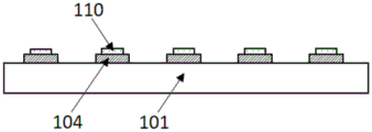
显示背板101,所述显示背板101上设有一组以上的金属焊盘组件104,每组所述金属焊盘组件104由两个金属焊盘组成,其分别为正极焊盘和负极焊盘,且该金属焊盘组件104由钛Ti、金Au、锡Sn、铜Cu、铟In、银Ag、铂Pt、铬Cr、镍Ni中的一种或几种金属通过图案化处理后所形成。并且该正极焊盘和负极焊盘的表面均通过导电胶110与微发光二极管芯片103下端的金属垫105相连接;其中,所述导电胶110为光固化导电胶,该导电胶110的主体包括:环氧树脂、硅酮,且其主体中掺杂有金属,其金属包括:银Ag、镍Ni、铜Cu的一种或几种组合。在本实施例中,通过在金属垫105与金属焊盘之间设置导电胶110,其能将与显示背板101进行键合前的微发光二极管芯片103临时固定在显示背板101上,便于在检测后对不良芯片进行替换,所述金属焊盘组件104的两侧分别设有遮光光阻,所述遮光光阻102包括:白色光阻或黑色光阻;在本实施例中,通过在显示背板101上设置遮光光阻102能有效地避免显示器发生漏光和混光的现象发生。所述微发光二极管芯片103和遮光光阻的上方覆盖有封装结构。所述封装结构包括从下到上依次覆盖的第一封装层106、第二封装层107、第三封装层108、第四封装层109;且第一封装层106的折射率大于第二封装层107的折射率、第二封装层107的折射率大于第三封装层108的折射率。The
实施例4Example 4
下面以一个垂直结构芯片显示器的实施例对本实用新型的一种微发光二极管显示器进行具体描述,请参阅图17,其包括:A micro-LED display of the present invention will be specifically described below with an embodiment of a vertical structure chip display, please refer to FIG. 17 , which includes:
显示背板101,所述显示背板101上设有一组以上的金属焊盘组件104,每组所述金属焊盘组件104由一个金属焊盘组成,且该金属焊盘组件104由钛Ti、金Au、锡Sn、铜Cu、铟In、银Ag、铂Pt、铬Cr、镍Ni中的一种或几种金属通过图案化处理后所形成。并且该金属焊盘的表面均通过导电胶110与微发光二极管芯片103下端的金属垫105相连接;其中,所述导电胶110为光固化导电胶,该导电胶110的主体包括:环氧树脂、硅酮,且其主体中掺杂有金属,其金属包括:银Ag、镍Ni、铜Cu的一种或几种组合。在本实施例中,通过在金属垫105与金属焊盘之间设置导电胶110,其能将与显示背板101进行键合前的微发光二极管芯片103临时固定在显示背板101上,便于在检测后对不良芯片进行替换,所述金属焊盘组件104的两侧分别设有遮光光阻,所述遮光光阻102包括:白色光阻或黑色光阻;在本实施例中,通过在显示背板101上设置遮光光阻102能有效地避免显示器发生漏光和混光的现象发生。所述微发光二极管芯片103的上端设有电极111,其中,该电极111由透明导电材料氧化铟锡ITO构成,所述微发光二极管芯片103和遮光光阻的上方覆盖有封装结构。所述封装结构包括从下到上依次覆盖的第一封装层106、第二封装层107、第三封装层108、第四封装层109;且第一封装层106的折射率大于第二封装层107的折射率、第二封装层107的折射率大于第三封装层108的折射率。The
实施例5Example 5
下面以一个实施例对本实用新型的一种应用于微发光二极管显示器的检测装置进行具体描述,请参阅图18,其包括:A detection device applied to a micro-LED display of the present invention will be specifically described below with an embodiment, please refer to FIG. 18 , which includes:
承载基板2021,所述承载基板2021上设有一个以上的电极结构2022,所述电极结构2022设于该承载基板2021的下表面,每个所述电极结构2022均用于与一个所述微发光二极管芯片103相连接,所述承载基板2021上连接有电源,所述电源用于为所述电极结构2022进行供电;故当需要进行检测时,承载基板2021上的电极结构2022与微发光二极管103对接,并对该微发光二极管103进行供电,以对微发光二极管103进行检测;所述承载基板2021上设有向其下表面凸起的凸台2023,所述电极结构2022覆盖于所述凸台2023上,其使得电极结构2022更便于于微发光二极管103相连接。A
在本说明书的描述中,参考术语“一个实施方式”、“一些实施方式”、“示意性实施方式”、“示例”、“具体示例”、或“一些示例”等的描述意指结合实施方式或示例描述的具体特征、结构、材料或者特点包含于本实用新型的至少一个实施方式或示例中。在本说明书中,对上述术语的示意性表述不一定指的是相同的实施方式或示例。而且,描述的具体特征、结构、材料或者特点可以在任何的一个或多个实施方式或示例中以合适的方式结合。In the description of this specification, reference to the terms "one embodiment," "some embodiments," "exemplary embodiment," "example," "specific example," or "some examples", etc., is meant to incorporate the embodiments A particular feature, structure, material, or characteristic described or exemplified is included in at least one embodiment or example of the present invention. In this specification, schematic representations of the above terms do not necessarily refer to the same embodiment or example. Furthermore, the particular features, structures, materials or characteristics described may be combined in any suitable manner in any one or more embodiments or examples.
以上所述仅为本实用新型的较佳实施例而已,并不用以限制本实用新型,凡在本实用新型的精神和原则之内所作的任何修改、等同替换和改进等,均应包含在本实用新型的保护范围之内。The above are only preferred embodiments of the present invention, and are not intended to limit the present invention. Any modifications, equivalent replacements and improvements made within the spirit and principles of the present invention shall be included in the present invention. within the scope of protection of the utility model.
Claims (7)
Priority Applications (1)
| Application Number | Priority Date | Filing Date | Title |
|---|---|---|---|
| CN202020387215.4U CN211604646U (en) | 2020-03-24 | 2020-03-24 | A micro light-emitting diode display and its detection device |
Applications Claiming Priority (1)
| Application Number | Priority Date | Filing Date | Title |
|---|---|---|---|
| CN202020387215.4U CN211604646U (en) | 2020-03-24 | 2020-03-24 | A micro light-emitting diode display and its detection device |
Publications (1)
| Publication Number | Publication Date |
|---|---|
| CN211604646U true CN211604646U (en) | 2020-09-29 |
Family
ID=72582769
Family Applications (1)
| Application Number | Title | Priority Date | Filing Date |
|---|---|---|---|
| CN202020387215.4U Active CN211604646U (en) | 2020-03-24 | 2020-03-24 | A micro light-emitting diode display and its detection device |
Country Status (1)
| Country | Link |
|---|---|
| CN (1) | CN211604646U (en) |
Cited By (6)
| Publication number | Priority date | Publication date | Assignee | Title |
|---|---|---|---|---|
| CN112858954A (en) * | 2021-01-12 | 2021-05-28 | 深圳市华星光电半导体显示技术有限公司 | Detection jig and detection method for detecting miniature light-emitting diode backlight module |
| CN113447716A (en) * | 2020-12-09 | 2021-09-28 | 重庆康佳光电技术研究院有限公司 | Display panel detection method and display panel |
| CN113659058A (en) * | 2021-08-20 | 2021-11-16 | 京东方科技集团股份有限公司 | Light-emitting device, preparation method thereof and display device |
| TWI748856B (en) * | 2021-01-29 | 2021-12-01 | 錼創顯示科技股份有限公司 | Micro light-emitting diode and display panel |
| CN115020394A (en) * | 2021-08-30 | 2022-09-06 | 友达光电股份有限公司 | Display assembly, display device comprising same and manufacturing method of display device |
| US12107190B2 (en) | 2021-01-29 | 2024-10-01 | PlayNitride Display Co., Ltd. | Micro light-emitting diode and display panel |
-
2020
- 2020-03-24 CN CN202020387215.4U patent/CN211604646U/en active Active
Cited By (11)
| Publication number | Priority date | Publication date | Assignee | Title |
|---|---|---|---|---|
| CN113447716A (en) * | 2020-12-09 | 2021-09-28 | 重庆康佳光电技术研究院有限公司 | Display panel detection method and display panel |
| CN113447716B (en) * | 2020-12-09 | 2022-04-29 | 重庆康佳光电技术研究院有限公司 | Display panel detection method and display panel |
| CN112858954A (en) * | 2021-01-12 | 2021-05-28 | 深圳市华星光电半导体显示技术有限公司 | Detection jig and detection method for detecting miniature light-emitting diode backlight module |
| CN112858954B (en) * | 2021-01-12 | 2023-10-13 | 深圳市华星光电半导体显示技术有限公司 | Detection jig and detection method for detecting miniature light-emitting diode backlight module |
| TWI748856B (en) * | 2021-01-29 | 2021-12-01 | 錼創顯示科技股份有限公司 | Micro light-emitting diode and display panel |
| US12021171B2 (en) | 2021-01-29 | 2024-06-25 | PlayNitride Display Co., Ltd. | Micro light emitting diode and display panel having etch protection conductive layer |
| US12107190B2 (en) | 2021-01-29 | 2024-10-01 | PlayNitride Display Co., Ltd. | Micro light-emitting diode and display panel |
| CN113659058A (en) * | 2021-08-20 | 2021-11-16 | 京东方科技集团股份有限公司 | Light-emitting device, preparation method thereof and display device |
| CN113659058B (en) * | 2021-08-20 | 2023-10-20 | 京东方科技集团股份有限公司 | Light-emitting device, preparation method thereof and display device |
| CN115020394A (en) * | 2021-08-30 | 2022-09-06 | 友达光电股份有限公司 | Display assembly, display device comprising same and manufacturing method of display device |
| CN115020394B (en) * | 2021-08-30 | 2025-11-11 | 友达光电股份有限公司 | Display assembly, display device comprising same and manufacturing method of display device |
Similar Documents
| Publication | Publication Date | Title |
|---|---|---|
| CN211604646U (en) | A micro light-emitting diode display and its detection device | |
| CN113450681A (en) | Production detection method of micro light-emitting diode display and display thereof | |
| US20210119098A1 (en) | Substrate mounting method and electronic-component-mounted substrate | |
| CN109920814B (en) | Display substrate, manufacturing method and display device | |
| CN110796956A (en) | A flexible transparent display screen and method of making the same | |
| CN113013067B (en) | Transfer method with detection and repair chip | |
| CN114496993B (en) | Chip detection plate, chip transfer method, display backboard and display device | |
| TW201212303A (en) | LED packaging structure and packaging method thereof | |
| CN111162154A (en) | Ultraviolet light-emitting element and all-inorganic packaging method | |
| US12015113B2 (en) | Bonding method, display backplane and system for manufacturing display backplane | |
| JPH03290936A (en) | Method of mounting semiconductor device | |
| CN201956388U (en) | Softly connected LED (light-emitting diode) device based on liquid metal substrate | |
| CN113451490B (en) | Bonding method, display back plate and display back plate manufacturing system | |
| CN212161854U (en) | A flexible transparent display reflow soldering fixture device | |
| KR20240003434A (en) | Light emitting substrate, manufacturing method and display device thereof | |
| CN110970457A (en) | Micro-LED chip, preparation method thereof and display device | |
| US12218298B2 (en) | Display panel and method for making the same | |
| CN211320106U (en) | Micro light-emitting diode display | |
| CN116190499B (en) | Display panel, preparation method thereof and display device | |
| CN101640245A (en) | Flip-chip packaging method for light emitting diode | |
| US20210090907A1 (en) | Encapsulation Method for Flip Chip | |
| JP3340779B2 (en) | Semiconductor device | |
| CN115241343A (en) | A kind of LED package device and preparation method and display device thereof | |
| CN115662313A (en) | Novel flip chip transparent screen and preparation process thereof | |
| CN114975712A (en) | A kind of micro LED chip quality detection structure and detection method |
Legal Events
| Date | Code | Title | Description |
|---|---|---|---|
| GR01 | Patent grant | ||
| GR01 | Patent grant | ||
| CP03 | Change of name, title or address | ||
| CP03 | Change of name, title or address |
Address after: 402760 No.69, Wushan Road, Biquan street, Bishan District, Chongqing Patentee after: Chongqing Kangjia Optoelectronic Technology Co.,Ltd. Country or region after: China Address before: 402760 No.69, Wushan Road, Biquan street, Bishan District, Chongqing Patentee before: Chongqing Kangjia Photoelectric Technology Research Institute Co.,Ltd. Country or region before: China |