CN1967800A - 半导体集成电路器件的制造方法 - Google Patents
半导体集成电路器件的制造方法 Download PDFInfo
- Publication number
- CN1967800A CN1967800A CNA200610146568XA CN200610146568A CN1967800A CN 1967800 A CN1967800 A CN 1967800A CN A200610146568X A CNA200610146568X A CN A200610146568XA CN 200610146568 A CN200610146568 A CN 200610146568A CN 1967800 A CN1967800 A CN 1967800A
- Authority
- CN
- China
- Prior art keywords
- film
- insulating film
- wiring
- mentioned
- forming
- Prior art date
- Legal status (The legal status is an assumption and is not a legal conclusion. Google has not performed a legal analysis and makes no representation as to the accuracy of the status listed.)
- Granted
Links
- 239000004065 semiconductor Substances 0.000 title claims abstract description 74
- 238000000034 method Methods 0.000 title claims abstract description 25
- 230000015572 biosynthetic process Effects 0.000 claims abstract description 44
- 229910052751 metal Inorganic materials 0.000 claims abstract description 35
- 239000002184 metal Substances 0.000 claims abstract description 35
- 238000004519 manufacturing process Methods 0.000 claims abstract description 30
- 239000004020 conductor Substances 0.000 claims description 24
- 229910052802 copper Inorganic materials 0.000 claims description 24
- 239000000758 substrate Substances 0.000 claims description 15
- 238000005530 etching Methods 0.000 claims description 12
- 229910052721 tungsten Inorganic materials 0.000 claims description 12
- 239000000463 material Substances 0.000 claims description 11
- 229910052737 gold Inorganic materials 0.000 claims description 9
- 239000011248 coating agent Substances 0.000 claims description 8
- 238000000576 coating method Methods 0.000 claims description 8
- 229910052782 aluminium Inorganic materials 0.000 claims description 5
- 239000012528 membrane Substances 0.000 claims description 5
- 229910052709 silver Inorganic materials 0.000 claims description 5
- 229910052804 chromium Inorganic materials 0.000 claims description 4
- 150000002736 metal compounds Chemical class 0.000 claims description 4
- 229910052759 nickel Inorganic materials 0.000 claims description 4
- 239000011229 interlayer Substances 0.000 abstract description 24
- 230000003071 parasitic effect Effects 0.000 abstract description 9
- 230000007547 defect Effects 0.000 abstract 1
- 239000010410 layer Substances 0.000 description 31
- 230000009977 dual effect Effects 0.000 description 24
- 239000010949 copper Substances 0.000 description 23
- RYGMFSIKBFXOCR-UHFFFAOYSA-N Copper Chemical compound [Cu] RYGMFSIKBFXOCR-UHFFFAOYSA-N 0.000 description 21
- 238000004544 sputter deposition Methods 0.000 description 16
- 238000000151 deposition Methods 0.000 description 14
- 238000005516 engineering process Methods 0.000 description 13
- 229910052715 tantalum Inorganic materials 0.000 description 13
- GUVRBAGPIYLISA-UHFFFAOYSA-N tantalum atom Chemical compound [Ta] GUVRBAGPIYLISA-UHFFFAOYSA-N 0.000 description 13
- MZLGASXMSKOWSE-UHFFFAOYSA-N tantalum nitride Chemical compound [Ta]#N MZLGASXMSKOWSE-UHFFFAOYSA-N 0.000 description 11
- 238000009713 electroplating Methods 0.000 description 8
- 238000009792 diffusion process Methods 0.000 description 7
- 238000010438 heat treatment Methods 0.000 description 7
- UFHFLCQGNIYNRP-UHFFFAOYSA-N Hydrogen Chemical compound [H][H] UFHFLCQGNIYNRP-UHFFFAOYSA-N 0.000 description 6
- 229910052739 hydrogen Inorganic materials 0.000 description 6
- 239000001257 hydrogen Substances 0.000 description 6
- 239000010936 titanium Substances 0.000 description 6
- 229910045601 alloy Inorganic materials 0.000 description 5
- 239000000956 alloy Substances 0.000 description 5
- 230000004888 barrier function Effects 0.000 description 5
- 230000000149 penetrating effect Effects 0.000 description 5
- 238000005229 chemical vapour deposition Methods 0.000 description 4
- 238000000227 grinding Methods 0.000 description 4
- 229910021420 polycrystalline silicon Inorganic materials 0.000 description 4
- 229910052719 titanium Inorganic materials 0.000 description 4
- RTAQQCXQSZGOHL-UHFFFAOYSA-N Titanium Chemical compound [Ti] RTAQQCXQSZGOHL-UHFFFAOYSA-N 0.000 description 3
- NRTOMJZYCJJWKI-UHFFFAOYSA-N Titanium nitride Chemical compound [Ti]#N NRTOMJZYCJJWKI-UHFFFAOYSA-N 0.000 description 3
- 238000004140 cleaning Methods 0.000 description 3
- 238000000206 photolithography Methods 0.000 description 3
- 229920000642 polymer Polymers 0.000 description 3
- WFKWXMTUELFFGS-UHFFFAOYSA-N tungsten Chemical compound [W] WFKWXMTUELFFGS-UHFFFAOYSA-N 0.000 description 3
- 239000010937 tungsten Substances 0.000 description 3
- 238000001312 dry etching Methods 0.000 description 2
- 238000005260 corrosion Methods 0.000 description 1
- 229910021419 crystalline silicon Inorganic materials 0.000 description 1
- 238000007872 degassing Methods 0.000 description 1
- 230000000694 effects Effects 0.000 description 1
- 230000010354 integration Effects 0.000 description 1
- 150000004767 nitrides Chemical class 0.000 description 1
- 229910021332 silicide Inorganic materials 0.000 description 1
- FVBUAEGBCNSCDD-UHFFFAOYSA-N silicide(4-) Chemical compound [Si-4] FVBUAEGBCNSCDD-UHFFFAOYSA-N 0.000 description 1
Images


Classifications
-
- H—ELECTRICITY
- H01—ELECTRIC ELEMENTS
- H01L—SEMICONDUCTOR DEVICES NOT COVERED BY CLASS H10
- H01L21/00—Processes or apparatus adapted for the manufacture or treatment of semiconductor or solid state devices or of parts thereof
- H01L21/70—Manufacture or treatment of devices consisting of a plurality of solid state components formed in or on a common substrate or of parts thereof; Manufacture of integrated circuit devices or of parts thereof
- H01L21/71—Manufacture of specific parts of devices defined in group H01L21/70
- H01L21/768—Applying interconnections to be used for carrying current between separate components within a device comprising conductors and dielectrics
- H01L21/76801—Applying interconnections to be used for carrying current between separate components within a device comprising conductors and dielectrics characterised by the formation and the after-treatment of the dielectrics, e.g. smoothing
- H01L21/7682—Applying interconnections to be used for carrying current between separate components within a device comprising conductors and dielectrics characterised by the formation and the after-treatment of the dielectrics, e.g. smoothing the dielectric comprising air gaps
-
- H—ELECTRICITY
- H01—ELECTRIC ELEMENTS
- H01L—SEMICONDUCTOR DEVICES NOT COVERED BY CLASS H10
- H01L21/00—Processes or apparatus adapted for the manufacture or treatment of semiconductor or solid state devices or of parts thereof
- H01L21/70—Manufacture or treatment of devices consisting of a plurality of solid state components formed in or on a common substrate or of parts thereof; Manufacture of integrated circuit devices or of parts thereof
- H01L21/71—Manufacture of specific parts of devices defined in group H01L21/70
- H01L21/768—Applying interconnections to be used for carrying current between separate components within a device comprising conductors and dielectrics
- H01L21/76801—Applying interconnections to be used for carrying current between separate components within a device comprising conductors and dielectrics characterised by the formation and the after-treatment of the dielectrics, e.g. smoothing
- H01L21/76802—Applying interconnections to be used for carrying current between separate components within a device comprising conductors and dielectrics characterised by the formation and the after-treatment of the dielectrics, e.g. smoothing by forming openings in dielectrics
- H01L21/76807—Applying interconnections to be used for carrying current between separate components within a device comprising conductors and dielectrics characterised by the formation and the after-treatment of the dielectrics, e.g. smoothing by forming openings in dielectrics for dual damascene structures
-
- H—ELECTRICITY
- H01—ELECTRIC ELEMENTS
- H01L—SEMICONDUCTOR DEVICES NOT COVERED BY CLASS H10
- H01L21/00—Processes or apparatus adapted for the manufacture or treatment of semiconductor or solid state devices or of parts thereof
- H01L21/70—Manufacture or treatment of devices consisting of a plurality of solid state components formed in or on a common substrate or of parts thereof; Manufacture of integrated circuit devices or of parts thereof
- H01L21/71—Manufacture of specific parts of devices defined in group H01L21/70
- H01L21/768—Applying interconnections to be used for carrying current between separate components within a device comprising conductors and dielectrics
- H01L21/76801—Applying interconnections to be used for carrying current between separate components within a device comprising conductors and dielectrics characterised by the formation and the after-treatment of the dielectrics, e.g. smoothing
- H01L21/76802—Applying interconnections to be used for carrying current between separate components within a device comprising conductors and dielectrics characterised by the formation and the after-treatment of the dielectrics, e.g. smoothing by forming openings in dielectrics
- H01L21/76814—Applying interconnections to be used for carrying current between separate components within a device comprising conductors and dielectrics characterised by the formation and the after-treatment of the dielectrics, e.g. smoothing by forming openings in dielectrics post-treatment or after-treatment, e.g. cleaning or removal of oxides on underlying conductors
-
- H—ELECTRICITY
- H01—ELECTRIC ELEMENTS
- H01L—SEMICONDUCTOR DEVICES NOT COVERED BY CLASS H10
- H01L21/00—Processes or apparatus adapted for the manufacture or treatment of semiconductor or solid state devices or of parts thereof
- H01L21/70—Manufacture or treatment of devices consisting of a plurality of solid state components formed in or on a common substrate or of parts thereof; Manufacture of integrated circuit devices or of parts thereof
- H01L21/71—Manufacture of specific parts of devices defined in group H01L21/70
- H01L21/768—Applying interconnections to be used for carrying current between separate components within a device comprising conductors and dielectrics
- H01L21/76801—Applying interconnections to be used for carrying current between separate components within a device comprising conductors and dielectrics characterised by the formation and the after-treatment of the dielectrics, e.g. smoothing
- H01L21/76829—Applying interconnections to be used for carrying current between separate components within a device comprising conductors and dielectrics characterised by the formation and the after-treatment of the dielectrics, e.g. smoothing characterised by the formation of thin functional dielectric layers, e.g. dielectric etch-stop, barrier, capping or liner layers
- H01L21/76831—Applying interconnections to be used for carrying current between separate components within a device comprising conductors and dielectrics characterised by the formation and the after-treatment of the dielectrics, e.g. smoothing characterised by the formation of thin functional dielectric layers, e.g. dielectric etch-stop, barrier, capping or liner layers in via holes or trenches, e.g. non-conductive sidewall liners
-
- H—ELECTRICITY
- H01—ELECTRIC ELEMENTS
- H01L—SEMICONDUCTOR DEVICES NOT COVERED BY CLASS H10
- H01L21/00—Processes or apparatus adapted for the manufacture or treatment of semiconductor or solid state devices or of parts thereof
- H01L21/70—Manufacture or treatment of devices consisting of a plurality of solid state components formed in or on a common substrate or of parts thereof; Manufacture of integrated circuit devices or of parts thereof
- H01L21/71—Manufacture of specific parts of devices defined in group H01L21/70
- H01L21/768—Applying interconnections to be used for carrying current between separate components within a device comprising conductors and dielectrics
- H01L21/76801—Applying interconnections to be used for carrying current between separate components within a device comprising conductors and dielectrics characterised by the formation and the after-treatment of the dielectrics, e.g. smoothing
- H01L21/76829—Applying interconnections to be used for carrying current between separate components within a device comprising conductors and dielectrics characterised by the formation and the after-treatment of the dielectrics, e.g. smoothing characterised by the formation of thin functional dielectric layers, e.g. dielectric etch-stop, barrier, capping or liner layers
- H01L21/76834—Applying interconnections to be used for carrying current between separate components within a device comprising conductors and dielectrics characterised by the formation and the after-treatment of the dielectrics, e.g. smoothing characterised by the formation of thin functional dielectric layers, e.g. dielectric etch-stop, barrier, capping or liner layers formation of thin insulating films on the sidewalls or on top of conductors
-
- H—ELECTRICITY
- H01—ELECTRIC ELEMENTS
- H01L—SEMICONDUCTOR DEVICES NOT COVERED BY CLASS H10
- H01L23/00—Details of semiconductor or other solid state devices
- H01L23/52—Arrangements for conducting electric current within the device in operation from one component to another, i.e. interconnections, e.g. wires, lead frames
- H01L23/522—Arrangements for conducting electric current within the device in operation from one component to another, i.e. interconnections, e.g. wires, lead frames including external interconnections consisting of a multilayer structure of conductive and insulating layers inseparably formed on the semiconductor body
- H01L23/5222—Capacitive arrangements or effects of, or between wiring layers
-
- H—ELECTRICITY
- H01—ELECTRIC ELEMENTS
- H01L—SEMICONDUCTOR DEVICES NOT COVERED BY CLASS H10
- H01L23/00—Details of semiconductor or other solid state devices
- H01L23/52—Arrangements for conducting electric current within the device in operation from one component to another, i.e. interconnections, e.g. wires, lead frames
- H01L23/522—Arrangements for conducting electric current within the device in operation from one component to another, i.e. interconnections, e.g. wires, lead frames including external interconnections consisting of a multilayer structure of conductive and insulating layers inseparably formed on the semiconductor body
- H01L23/532—Arrangements for conducting electric current within the device in operation from one component to another, i.e. interconnections, e.g. wires, lead frames including external interconnections consisting of a multilayer structure of conductive and insulating layers inseparably formed on the semiconductor body characterised by the materials
- H01L23/53204—Conductive materials
- H01L23/53209—Conductive materials based on metals, e.g. alloys, metal silicides
- H01L23/53214—Conductive materials based on metals, e.g. alloys, metal silicides the principal metal being aluminium
- H01L23/53223—Additional layers associated with aluminium layers, e.g. adhesion, barrier, cladding layers
-
- H—ELECTRICITY
- H01—ELECTRIC ELEMENTS
- H01L—SEMICONDUCTOR DEVICES NOT COVERED BY CLASS H10
- H01L23/00—Details of semiconductor or other solid state devices
- H01L23/52—Arrangements for conducting electric current within the device in operation from one component to another, i.e. interconnections, e.g. wires, lead frames
- H01L23/522—Arrangements for conducting electric current within the device in operation from one component to another, i.e. interconnections, e.g. wires, lead frames including external interconnections consisting of a multilayer structure of conductive and insulating layers inseparably formed on the semiconductor body
- H01L23/532—Arrangements for conducting electric current within the device in operation from one component to another, i.e. interconnections, e.g. wires, lead frames including external interconnections consisting of a multilayer structure of conductive and insulating layers inseparably formed on the semiconductor body characterised by the materials
- H01L23/53204—Conductive materials
- H01L23/53209—Conductive materials based on metals, e.g. alloys, metal silicides
- H01L23/53228—Conductive materials based on metals, e.g. alloys, metal silicides the principal metal being copper
- H01L23/53238—Additional layers associated with copper layers, e.g. adhesion, barrier, cladding layers
-
- H—ELECTRICITY
- H01—ELECTRIC ELEMENTS
- H01L—SEMICONDUCTOR DEVICES NOT COVERED BY CLASS H10
- H01L23/00—Details of semiconductor or other solid state devices
- H01L23/52—Arrangements for conducting electric current within the device in operation from one component to another, i.e. interconnections, e.g. wires, lead frames
- H01L23/522—Arrangements for conducting electric current within the device in operation from one component to another, i.e. interconnections, e.g. wires, lead frames including external interconnections consisting of a multilayer structure of conductive and insulating layers inseparably formed on the semiconductor body
- H01L23/532—Arrangements for conducting electric current within the device in operation from one component to another, i.e. interconnections, e.g. wires, lead frames including external interconnections consisting of a multilayer structure of conductive and insulating layers inseparably formed on the semiconductor body characterised by the materials
- H01L23/53204—Conductive materials
- H01L23/53209—Conductive materials based on metals, e.g. alloys, metal silicides
- H01L23/53242—Conductive materials based on metals, e.g. alloys, metal silicides the principal metal being a noble metal, e.g. gold
- H01L23/53252—Additional layers associated with noble-metal layers, e.g. adhesion, barrier, cladding layers
-
- H—ELECTRICITY
- H01—ELECTRIC ELEMENTS
- H01L—SEMICONDUCTOR DEVICES NOT COVERED BY CLASS H10
- H01L23/00—Details of semiconductor or other solid state devices
- H01L23/52—Arrangements for conducting electric current within the device in operation from one component to another, i.e. interconnections, e.g. wires, lead frames
- H01L23/522—Arrangements for conducting electric current within the device in operation from one component to another, i.e. interconnections, e.g. wires, lead frames including external interconnections consisting of a multilayer structure of conductive and insulating layers inseparably formed on the semiconductor body
- H01L23/532—Arrangements for conducting electric current within the device in operation from one component to another, i.e. interconnections, e.g. wires, lead frames including external interconnections consisting of a multilayer structure of conductive and insulating layers inseparably formed on the semiconductor body characterised by the materials
- H01L23/53204—Conductive materials
- H01L23/53209—Conductive materials based on metals, e.g. alloys, metal silicides
- H01L23/53257—Conductive materials based on metals, e.g. alloys, metal silicides the principal metal being a refractory metal
- H01L23/53266—Additional layers associated with refractory-metal layers, e.g. adhesion, barrier, cladding layers
-
- H—ELECTRICITY
- H01—ELECTRIC ELEMENTS
- H01L—SEMICONDUCTOR DEVICES NOT COVERED BY CLASS H10
- H01L23/00—Details of semiconductor or other solid state devices
- H01L23/52—Arrangements for conducting electric current within the device in operation from one component to another, i.e. interconnections, e.g. wires, lead frames
- H01L23/522—Arrangements for conducting electric current within the device in operation from one component to another, i.e. interconnections, e.g. wires, lead frames including external interconnections consisting of a multilayer structure of conductive and insulating layers inseparably formed on the semiconductor body
- H01L23/532—Arrangements for conducting electric current within the device in operation from one component to another, i.e. interconnections, e.g. wires, lead frames including external interconnections consisting of a multilayer structure of conductive and insulating layers inseparably formed on the semiconductor body characterised by the materials
- H01L23/5329—Insulating materials
- H01L23/53295—Stacked insulating layers
-
- H—ELECTRICITY
- H01—ELECTRIC ELEMENTS
- H01L—SEMICONDUCTOR DEVICES NOT COVERED BY CLASS H10
- H01L21/00—Processes or apparatus adapted for the manufacture or treatment of semiconductor or solid state devices or of parts thereof
- H01L21/70—Manufacture or treatment of devices consisting of a plurality of solid state components formed in or on a common substrate or of parts thereof; Manufacture of integrated circuit devices or of parts thereof
- H01L21/71—Manufacture of specific parts of devices defined in group H01L21/70
- H01L21/768—Applying interconnections to be used for carrying current between separate components within a device comprising conductors and dielectrics
- H01L21/76838—Applying interconnections to be used for carrying current between separate components within a device comprising conductors and dielectrics characterised by the formation and the after-treatment of the conductors
- H01L21/76841—Barrier, adhesion or liner layers
- H01L21/76843—Barrier, adhesion or liner layers formed in openings in a dielectric
- H01L21/76849—Barrier, adhesion or liner layers formed in openings in a dielectric the layer being positioned on top of the main fill metal
-
- H—ELECTRICITY
- H01—ELECTRIC ELEMENTS
- H01L—SEMICONDUCTOR DEVICES NOT COVERED BY CLASS H10
- H01L2221/00—Processes or apparatus adapted for the manufacture or treatment of semiconductor or solid state devices or of parts thereof covered by H01L21/00
- H01L2221/10—Applying interconnections to be used for carrying current between separate components within a device
- H01L2221/1005—Formation and after-treatment of dielectrics
- H01L2221/101—Forming openings in dielectrics
- H01L2221/1015—Forming openings in dielectrics for dual damascene structures
- H01L2221/1026—Forming openings in dielectrics for dual damascene structures the via being formed by burying a sacrificial pillar in the dielectric and removing the pillar
-
- H—ELECTRICITY
- H01—ELECTRIC ELEMENTS
- H01L—SEMICONDUCTOR DEVICES NOT COVERED BY CLASS H10
- H01L2924/00—Indexing scheme for arrangements or methods for connecting or disconnecting semiconductor or solid-state bodies as covered by H01L24/00
- H01L2924/0001—Technical content checked by a classifier
- H01L2924/0002—Not covered by any one of groups H01L24/00, H01L24/00 and H01L2224/00
Landscapes
- Engineering & Computer Science (AREA)
- Physics & Mathematics (AREA)
- Condensed Matter Physics & Semiconductors (AREA)
- General Physics & Mathematics (AREA)
- Computer Hardware Design (AREA)
- Microelectronics & Electronic Packaging (AREA)
- Power Engineering (AREA)
- Manufacturing & Machinery (AREA)
- Internal Circuitry In Semiconductor Integrated Circuit Devices (AREA)
Abstract
本发明提供一种半导体集成电路器件的制造方法,防止具有空气隙(Air-Gap)结构的多层镶嵌布线中的、偏移通孔的金属形成不良。在连接孔的形成区域,使用可有选择地除去的绝缘膜形成牺牲膜柱(42)之后,在相邻的镶嵌布线间形成具有空气隙(Air-Gap)(45)的层间绝缘膜(44),由此完全分离通孔和空气隙(45)。根据本发明,能够形成具有可靠性高的通孔连接、能减小因空气隙引起的寄生电容的多层嵌入布线。
Description
技术领域
本发明涉及半导体集成电路器件的制造方法,尤其涉及具有多层嵌入布线的半导体集成电路器件的制造方法。
背景技术
嵌入布线结构,是通过在绝缘膜上形成的布线沟或连接孔等这样的布线开口部内,利用称为镶嵌(Damascene)技术(单镶嵌(Single-Damascene)技术以及双镶嵌(Dual-Damascene)技术)的布线形成技术嵌入布线材料而形成的。
近年来,这样的嵌入布线的间隔随着半导体集成电路器件的高度集成化而日益减小。由此,布线间的寄生电容增大而产生信号延迟。因此,期望降低布线间的寄生电容。
专利文献1中,公开了在嵌入布线间形成空气隙的技术。该文献的图1A~1E,按工序示出了1层嵌入布线的制造方法。图示的技术的特征在于,由于介于相邻的嵌入布线间的绝缘膜含有空气隙,所以能够降低相邻的嵌入布线间的寄生电容。
专利文献1:美国专利第6,159,845号说明书
发明内容
在专利文献1中,没有载明关于具有空气隙结构的多层嵌入布线的制造方法。经本申请的发明人等的研究,明确了使用专利文献1的技术形成多层嵌入布线时,产生由通孔(Via)部的金属嵌入不良引起通孔部的高电阻化的问题以及金属在空气隙中成膜而不能降低相邻的嵌入布线间的寄生电容的问题。如图2所示,其原因在于,由于在通常的光刻工序中的下层嵌入布线(单镶嵌布线)65与上层嵌入布线(双镶嵌布线)68的通孔部66之间的对合偏移,通孔部66接触下层嵌入布线65间的空气隙67,因此在包含通孔部66的上层嵌入布线68的金属成膜时,产生金属向空气隙的侵入69或通孔部的金属嵌入不良70。
简单地说明本发明公开的技术方案的具有代表性的概要如下。
本发明的半导体集成电路器件的制造方法具有以下步骤:
(a)在半导体衬底的上方形成第1绝缘膜;
(b)在上述第1绝缘膜上形成多个布线沟;
(c)在包含上述多个布线沟的每一个的内部的上述第1绝缘膜上形成第1导体膜;
(d)通过除去上述多个布线沟的外部的上述第1导体膜,在上述多个布线沟的每一个的内部形成由上述第1导体膜构成的布线;
(e)在上述第1绝缘膜以及上述布线上形成由与上述第1绝缘膜不同的材料构成的第2绝缘膜;
(f)使用覆盖要在后续步骤中形成的用于露出上述布线的上表面的连接孔的形成区域的掩膜,蚀刻上述第2绝缘膜,由此在上述连接孔的形成区域形成由上述第2绝缘膜构成的牺牲膜柱;
(g)有选择地除去未被上述牺牲膜柱覆盖的区域的上述第1绝缘膜,在上述牺牲膜柱的下部保留上述第1绝缘膜;
(h)在除去了上述第1绝缘膜的上述布线间的间隔区域保留空气隙,并且在上述布线以及上述牺牲膜柱上形成由与上述第2绝缘膜不同的材料构成的第3绝缘膜;
(i)除去上述牺牲膜柱上的上述第3绝缘膜,露出上述牺牲膜柱的上表面;
(j)除去上述牺牲膜柱,形成露出上述布线上表面的连接孔;
(k)在上述连接孔的内部形成第2导体膜。
本发明的半导体集成电路器件的制造方法具有以下工序:
(a)在半导体衬底的上方形成第1绝缘膜;
(b)通过除去上述第1绝缘膜的一部分,形成在后续步骤中的第1镶嵌布线用的多个第1布线沟;
(c)在包含上述多个第1布线沟的每一个的内部的上述第1绝缘膜上形成第1导体膜;
(d)通过除去上述多个第1布线沟的外部的上述第1导体膜,在上述多个第1布线沟的每一个的内部形成由上述第1导体膜构成的上述第1镶嵌布线;
(e)在上述第1绝缘膜以及上述第1镶嵌布线上形成由与上述第1绝缘膜不同的材料构成的第2绝缘膜;
(f)使用覆盖要在后续步骤中形成的第2镶嵌布线上的通孔部用的多个连接孔的形成区域的掩膜,蚀刻上述第2绝缘膜,由此在上述多个连接孔的形成区域形成由上述第2绝缘膜构成多个牺牲膜柱;
(g)有选择地除去未被上述牺牲膜柱覆盖的区域的上述第1绝缘膜,在上述牺牲膜柱的下部保留上述第1绝缘膜;
(h)在除去了上述第1绝缘膜的上述布线间的间隔区域保留空气隙,并且在上述布线以及上述牺牲膜柱上形成由与上述第2绝缘膜不同的材料构成的第3绝缘膜;
(i)除去上述牺牲膜柱上的上述第3绝缘膜,露出上述多个牺牲膜柱的上表面;
(j)通过除去上述第3绝缘膜的一部分以及上述多个牺牲膜柱的上部,形成后续步骤中形成的上述第2镶嵌布线的布线部用的多个第2布线沟;
(k)通过除去上述多个牺牲膜柱的下部,形成多个连接孔;
(l)在包含上述多个第2布线沟以及上述多个连接孔的每一个的内部的上述第3绝缘膜上,形成第2导体膜;
(m)通过除去上述多个第2布线沟以及上述多个连接孔的外部的上述第2导体膜,在上述多个第2布线沟以及上述多个连接孔的每一个的内部,形成由上述第2导体膜构成的上述第2镶嵌布线。
简单地说明本申请所公开的发明中具有代表性的发明取得的效果如下。
根据本发明,具有可靠性高的通孔连接,能够形成降低了因空气隙引起的寄生电容的多层嵌入布线。
附图说明
图1是表示本发明的实施例1的半导体器件的主要部分的纵剖视图。
图2是表示现有的具有空气隙结构的多层嵌入布线的问题点的纵剖视图。
图3是按工序表示本发明的实施例1的半导体器件的布线层形成的纵剖视图。
图4是按工序表示本发明的实施例1的半导体器件的布线层形成的纵剖视图。
图5是按工序表示本发明的实施例1的半导体器件的布线层形成的纵剖视图。
图6是按工序表示本发明的实施例1的半导体器件的布线层形成的纵剖视图。
图7是按工序表示本发明的实施例1的半导体器件的布线层形成的纵剖视图。
图8是按工序表示本发明的实施例1的半导体器件的布线层形成的纵剖视图。
图9是按工序表示本发明的实施例1的半导体器件的布线层形成的纵剖视图。
图10是按工序表示本发明的实施例1的半导体器件的布线层形成的纵剖视图。
图11是按工序表示本发明的实施例1的半导体器件的布线层形成的纵剖视图。
图12A是表示本发明的实施例1的半导体器件的主要部分的纵剖视图。
图12B是表示本发明的实施例1的半导体器件的主要部分的纵剖视图。
图13A是表示本发明的实施例1的半导体器件的主要部分的纵剖视图。
图13B是表示本发明的实施例1的半导体器件的主要部分的纵剖视图。
图13C是表示本发明的实施例1的半导体器件的主要部分的纵剖视图。
图14A是表示本发明的实施例1的半导体器件的主要部分的纵剖视图。
图14B是表示本发明的实施例1的半导体器件的主要部分的纵剖视图。
图15是表示本发明的实施例2的半导体器件的主要部分的纵剖视图。
图16是按工序表示本发明的实施例2的半导体器件的布线层形成的纵剖视图。
图17是按工序表示本发明的实施例2的半导体器件的布线层形成的纵剖视图。
图18是按工序表示本发明的实施例2的半导体器件的布线层形成的纵剖视图。
图19是表示本发明的实施例2的半导体器件的主要部分的纵剖视图。
图20是表示本发明的实施例3的半导体器件的主要部分的纵剖视图。
图21是按工序表示本发明的实施例3的半导体器件的布线层形成的纵剖视图。
图22是按工序表示本发明的实施例3的半导体器件的布线层形成的纵剖视图。
图23是按工序表示本发明的实施例3的半导体器件的布线层形成的纵剖视图。
具体实施方式
以下,根据附图详细说明本发明的实施例。在用于说明实施例的全部附图中,具有同一功能的部件采用同一标记,省略其反复的说明。另外,在以下的实施例中,除特别必要时以外,作为原则不重复说明相同或同样的部分。
[实施例1]
图1是表示本发明的实施例1的半导体器件的主要部分的剖视图。
用场绝缘膜2将半导体衬底1的主面分离成各元件区域,在各元件区域形成源极区域、漏极区域等的扩散层3,在源极区域、漏极区域3之间的半导体衬底1的主面上间隔栅极绝缘膜(未图示)形成多结晶硅构成的栅极电极4,栅极电极4的侧面被侧壁绝缘膜5覆盖。
形成于半导体衬底1的主面上的扩散层3或栅极电极4连接到贯通层间绝缘膜6的插塞7的一端,插塞7的另一端连接到隔着层间绝缘膜6层叠的单镶嵌布线10上。层间绝缘膜6,在顺次淀积了P-SiN膜(50nm)、HDP-SiO膜(400nm)、P-SiO膜(400nm)之后,使用CMP技术研磨500nm左右(大面积布线上的研磨量),使由栅极电极4等产生的元件台阶平坦化。
插塞7是在顺次淀积了由溅射形成的钛膜(10nm)、氮化钛膜(50nm)、用CVD形成的钨膜之后,用CMP加工而成的。
单镶嵌布线10,在顺次淀积了由溅射形成的氮化钽膜(15nm)、钽膜(15nm)、铜膜(80nm)、用电镀法形成的铜膜(500nm)之后,在氢氛围下进行400℃、2分钟的热处理,用CMP技术形成。
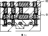
贯通在单镶嵌布线10的相邻间隔小的部分具有空气隙(Air-Gap)17的层间绝缘膜16,双镶嵌布线23连接到单镶嵌布线10上。此时,在处于与单镶嵌布线10错开的位置的双镶嵌布线23的通孔部下方残存有形成单镶嵌布线10时所使用的绝缘膜的一部分的膜15。
双镶嵌布线23、27、30与单镶嵌布线10相同地,在顺次淀积溅射形成的氮化钽膜(15nm)、钽膜(15nm)、铜膜(80nm)、用电镀法形成的铜膜(500nm)之后,在氢氛围下进行400℃、2分钟的热处理,由CMP技术形成。
贯通在双镶嵌布线23的相邻间隔小的部分具有空气隙25的层间绝缘膜26,双镶嵌布线27连接到双镶嵌布线23。此时,在处于与双镶嵌布线23错开的位置的双镶嵌布线27的通孔部下方残存有层间绝缘膜16的一部分的膜24。
贯通在双镶嵌布线27的相邻间隔小的部分具有空气隙28的层间绝缘膜29,双镶嵌布线30连接到双镶嵌布线27上。此时,在处于与双镶嵌布线27错开的位置的双镶嵌布线30的通孔部下方残存有层间绝缘膜26的一部分的膜31。
在本实施例中,由于通孔部和空气隙没有接连,所以能够防止由通孔部的金属嵌入不良引起的高电阻化和由金属向空气隙侵入引起的寄生电容增大的问题。
然后,关于本实施例1的半导体器件的制造方法,使用图3~11按工序进行说明。
首先,用场绝缘膜2将半导体衬底1的主面分离成各元件区域之后,在各元件区域形成源极区域、漏极区域等的扩散层3,在源极区域、漏极区域3之间的半导体衬底1的主面上隔着栅极绝缘膜(未图示)形成了由多结晶硅构成的栅极电极4之后,用侧壁绝缘膜5覆盖栅极电极4的侧面。
然后,在顺次淀积了P-SiN膜(50nm)、HDP-SiO膜(400nm)、P-SiO膜(400nm)之后,用CMP技术研磨500nm左右(大面积栅极上的研磨量),使由栅极电极4等产生的元件台阶平坦而形成层间绝缘膜6。
然后,用通常的光刻以及干蚀刻技术开口连接孔之后,用Ar等离子体除去连接孔底部的自然氧化膜,然后,顺次淀积由溅射形成的Ti/TiN膜7a(10/50nm)、用CVD法形成的W膜7b(300nm)之后,用CMP技术除去连接孔以外的Ti/TiN膜以及用CVD法形成的W膜,形成插塞7。
然后,在淀积SiCN/SiC膜8(25/25nm)、作为无机类绝缘膜的FSG膜(第1绝缘膜)9(300nm)之后,用通常的光刻以及干蚀刻技术形成用于形成布线10的沟。
然后,用Ar等离子体除去在沟底部露出的插塞7表面的自然氧化膜之后,顺次淀积作为阻挡金属膜的由溅射形成的氮化钽/钽膜10a(15/15nm)、作为主导体膜的由溅射形成的铜膜/用电镀法形成的铜膜(第1导体膜)10b(80/500nm)之后,在氢氛围下进行400℃、2分钟的热处理,用CMP技术除去沟以外的氮化钽/钽/铜膜,形成单镶嵌布线10。该状态如图3所示。
然后,淀积作为有机类绝缘膜的SiLK膜(第2绝缘膜)11(700nm)、P-TEOS膜12(100nm)之后,形成凸状的抗蚀剂13。抗蚀剂13为柱状,覆盖在后续工序中形成的连接孔的形成区域,该连接孔用于露出单镶嵌布线10的上表面。该状态如图4所示。
然后,以抗蚀剂13为掩膜蚀刻加工P-TEOS膜12,接着以抗蚀剂13以及P-TEOS12为掩膜蚀刻加工SiLK膜11,形成由SiLK膜构成的牺牲膜柱14。在该阶段残存有SiLK膜表面的P-TEOS膜12。
然后,各向异性蚀刻加工单镶嵌布线10间的FSG膜9,除去未被牺牲膜柱覆盖的区域的FSG膜9。此时,位于牺牲膜柱14下方的FSG膜9的一部分保留下来,形成FSG膜15。该状态如图5所示。
然后,形成作为无机类绝缘膜的FSG膜(第3绝缘膜)16(1200nm)。此时,使用CVD法在覆盖度(coverage)低的成膜条件下淀积FSG膜16,使得能够在单镶嵌布线10的相邻间隔小的部分形成空气隙17。另外,也可以是,对FSG膜16的形成使用CVD法,形成初期在覆盖度低的成膜条件下进行以形成空气隙,在形成空气隙17之后,在覆盖度高的成膜条件下进行而嵌入牺牲膜柱14。并且,FSG膜16必须淀积到其表面比牺牲膜柱14的上表面高那样的膜厚。该状态如图6所示。
然后,用CMP使FSG膜16的表面平坦化,并且使牺牲膜柱14的表面露出,形成由FSG膜构成的、用于形成双镶嵌布线的层间绝缘膜18。在该阶段,牺牲膜柱14的表面没有保留P-TEOS膜12。该状态如图7所示。
然后,形成用于形成双镶嵌布线的抗蚀剂图案20。该状态如图8所示。
然后,以抗蚀剂图案20为掩膜在蚀刻速率大致相同的条件下蚀刻加工牺牲膜柱14和层间绝缘膜18,由此形成双镶嵌布线的布线部用的沟21。该状态如图9所示。
然后,用NH3等离子体有选择地除去牺牲膜柱14,由此形成双镶嵌布线的通孔部用的连接孔22。该状态如图10所示。
然后,除去蚀刻聚合物并清洗后,与单镶嵌布线10的形成相同地,用Ar等离子体除去在连接孔22的底部露出的单镶嵌布线10表面的自然氧化膜之后,顺次淀积作为阻挡金属膜的由溅射形成的氮化钽/钽膜23a(15/15nm)、作为主导体膜的由溅射形成的铜膜/用电镀法形成的铜膜(第2导体膜)23b(80/500nm),然后,在氢氛围下进行400℃、2分钟的热处理,用CMP除去连接孔22和沟21以外的氮化钽/钽/铜膜,形成双镶嵌布线23。该状态如图11所示。
图1所示的状态表示多层的镶嵌布线,通过重复上述工序,在相邻的双镶嵌布线23之间以及双镶嵌布线27之间的间隔狭窄的部分形成有空气隙25、28。
在上述实施例中,表示了作为单镶嵌布线10和双镶嵌布线23的主导体膜使用Cu的例子,但不限于此,也可以使用Al、W、Ag、Au中的至少任意一种金属作为主导体膜。
在本实施例中,通过制作牺牲膜柱,使形成在相邻的镶嵌布线间的空气隙离开通孔部地形成,所以即使发生对合偏移,空气隙和通孔部也不接触,因此能够稳定地向具有空气隙结构的下层镶嵌布线上进行通孔连接。
在上述实施例中,形成镶嵌布线10、23等之后,在镶嵌布线表面有选择地形成作为金属覆层(metal cap)膜的CoWB合金32、33,由此能够提高镶嵌布线10、23等的可靠性。此外,作为金属覆层膜不限于上述CoWB合金,也能够使用Co、W、Ni、Cr、Au中的至少任意一种金属或金属化合物。该状态如图12(a)、(b)所示。
另外,在上述实施例中,在图9中,以蚀刻速率大致相同的条件蚀刻加工牺牲膜柱14和层间绝缘膜18,形成双镶嵌布线23的布线部用沟21,但也能够如图13(a)~(c)所示,仅将牺牲膜柱14的上部蚀刻到沟深度的程度,然后在层间绝缘膜18上形成沟35。然后,有选择地除去牺牲膜柱的下部34,形成连接孔36。在难以使牺牲膜柱14和层间绝缘膜18的蚀刻速率相等的情况下,该方法是有效的。
进一步,在图9或图13(b)所示的沟加工中,存在抗蚀剂20不足的情况,但此时能够如图14所示,增加P-SiN膜37,形成SiN硬掩膜38,将其作为掩膜对沟进行加工。
[实施例2]
图15是表示本发明的实施例2的半导体器件的主要部分的剖视图。
用场绝缘膜2将半导体衬底1的主面分离成各元件区域,在各元件区域形成源极区域、漏极区域的扩散层3,在源极区域、漏极区域3之间的半导体衬底1的主面上间隔栅极绝缘膜(未图示)形成由多结晶硅构成的栅极电极4,栅极电极4的侧面被侧壁绝缘膜5覆盖。
形成于半导体衬底1主面的扩散层3或栅极电极4,连接到贯通层间绝缘膜6的插塞7的一端,插塞7的另一端连接到隔着层间绝缘膜6层叠的单镶嵌布线10。层间绝缘膜6,在顺次淀积了P-SiN膜(50nm)、HDP-SiO膜(400nm)、P-SiO膜(400nm)之后,使用CMP技术研磨500nm左右(大面积布线上的研磨量),使由栅极电极4等产生的元件台阶平坦化。
插塞7是在顺次淀积由溅射形成的钛膜(10nm)、氮化钛膜(50nm)、用CVD形成的钨膜之后,用CMP技术加工而成的。
单镶嵌布线10,在顺次淀积由溅射形成的氮化钽膜(15nm)、钽膜(15nm)、铜膜(80nm)、用电镀法形成的铜膜(500nm)之后,在氢氛围下进行400℃、2分钟的热处理,用CMP技术形成。
双镶嵌布线49通过通孔46连接到单镶嵌布线10,该通孔46贯通在单镶嵌布线10的相邻间隔小的部分具有空气隙(Air-Gap)45的层间绝缘膜50。此时,在处于与单镶嵌布线10错开的位置的通孔46下部残存有形成单镶嵌布线10时所使用的绝缘膜的一部分的膜43。
在本实施例中,由于通孔和空气隙不接触,所以能够防止由通孔的金属嵌入不良引起的高电阻化和由金属向空气隙侵入引起的寄生电容增大的问题。
接下来,关于本实施例2的半导体器件的制造方法,使用图16~18按工序进行说明。
在实施例1的图3所示的工序之后,淀积作为有机类绝缘膜的SiLK膜(第2绝缘膜)39(400nm)、P-TEOS膜40(100nm),然后,形成凸状的抗蚀剂41。抗蚀剂41为柱状,覆盖在后续工序中形成的连接孔的形成区域,该连接孔用于露出单镶嵌布线10的上表面。该状态如图16所示。
然后,以抗蚀剂41为掩膜蚀刻加工P-TEOS膜40,接着以抗蚀剂41以及P-TEOS膜40为掩膜蚀刻加工SiLK膜39,形成由SiLK膜构成的牺牲膜柱42。在该阶段残存有SiLK膜表面的P-TEOS膜40。
然后,各向异性蚀刻加工单镶嵌布线10之间的FSG膜9,除去未被牺牲膜柱覆盖的区域的FSG膜9。此时,位于牺牲膜柱42下方的FSG膜9的一部分保留下来,形成FSG膜43。
然后,形成作为无机类绝缘膜的FSG膜(第3绝缘膜)(800nm)。此时,使用CVD法在覆盖度低的成膜条件下淀积FSG膜,使得在单镶嵌布线10的相邻间隔小的部分具有空气隙45。另外,也可以是,对于FSG膜的形成使用CVD法,形成初期在覆盖度低的成膜条件下进行以形成空气隙45,在形成空气隙45之后,在覆盖度高的成膜条件下进行以嵌入牺牲膜柱42。此外,FSG膜必须淀积到其表面比牺牲膜柱42的上表面高那样的膜厚。
然后,用CMP使FSG膜的表面平坦化,并且使牺牲膜柱42的表面露出,形成由FSG膜构成的、用于形成通孔的层间绝缘膜44。该状态如图17所示。
然后,用NH3等离子体有选择地除去牺牲膜柱42,由此开出到达单镶嵌布线10的连接孔。
然后,除去蚀刻聚合物并清洗后,用Ar等离子体除去在连接孔的底部露出的单镶嵌布线10表面的自然氧化膜,然后,顺次淀积作为阻挡金属膜的由溅射形成的氮化钽/钽膜(15/15nm)、作为主导体膜的由溅射形成的铜膜/用电镀法形成的铜膜(第2导体膜)(80/500nm)之后,在氢氛围下进行400℃、2分钟的热处理,用CMP除去连接孔以外的氮化钽/钽/铜膜,形成通孔46。该状态如图18所示。
然后,使用与形成单镶嵌布线10相同的方法,在淀积了SiCN/SiC膜47、作为无机类绝缘膜的FSG膜48之后形成沟,在该沟内形成单镶嵌布线49,以上如上述图15所示。
并且,虽未图示,但通过重复上述工序,也能够形成3层以上的多层镶嵌布线。
在上述实施例中,表示了作为单镶嵌布线10、49和通孔46的主导体膜使用了Cu的例子,但不限于此,也可以使用Al、W、Ag、Au中的至少任意一种金属作为主导体膜。
在本实施例中,通过制作牺牲膜柱,能够形成在相邻的镶嵌布线间的空气隙离开通孔部地形成,因此,即使发生对合偏移,空气隙和通孔部也不接触,因而能够稳定地向具有空气隙结构的下层镶嵌布线上进行通孔连接。
此外,在上述实施例中,形成镶嵌布线10、49等之后,在镶嵌布线表面有选择地形成作为金属覆层膜的CoWB合金51、52,由此能够提高镶嵌布线10、49等的可靠性。并且,作为金属覆层膜不限于上述CoWB合金,也能够使用Co、W、Ni、Cr、Au中的任意一种金属或金属化合物。该状态如图19所示。
另外,虽未图示,但也可以在通孔46的表面上形成CoWB合金。
另外,如图14所示,也能应用使用了P-SiN膜的硬掩膜加工。
[实施例3]
图20是表示本发明的实施例3的半导体器件的主要部分的剖视图。
用场绝缘膜2将半导体衬底1的主面分离成各元件区域,在各元件区域形成源极区域、漏极区域的扩散层3,在源极区域、漏极区域3之间的半导体衬底1的主面上隔着栅极绝缘膜(未图示)形成由多结晶硅构成的栅极电极4,栅极电极4的侧面被侧壁绝缘膜5覆盖。
形成于半导体衬底1的主面上的扩散层3或栅极电极4,连接到贯通层间绝缘膜6的插塞7的一端,插塞7的另一端连接到隔着层间绝缘膜6层叠的单镶嵌布线10。层间绝缘膜6,在顺次淀积P-SiN膜(50nm)、HDP-SiO膜(400nm)、P-SiO膜(400nm)之后,使用CMP技术研磨500nm左右(大面积布线上的研磨量),使由栅极电极4等产生的元件台阶平坦化。
插塞7是在顺次淀积溅射形成的钛膜(10nm)、氮化钛膜(50nm)、用CVD形成的钨膜之后,用CMP加工而成的。
单镶嵌布线10,在顺次淀积由溅射形成的氮化钽膜(15nm)、钽膜(15nm)、铜膜(80nm)、用电镀法形成的铜膜(500nm)之后,在氢氛围下进行400℃、2分钟的热处理,用CMP形成。
双镶嵌布线59通过通孔56连接到单镶嵌布线10,该通孔56贯通在单镶嵌布线10的相邻间隔小的部分具有空气隙(Air-Gap)55的层间绝缘膜54。此时,在处于与单镶嵌布线10错开的通孔56的下部残存有形成单镶嵌布线10时所使用的绝缘膜9的一部分的膜43。
另外,在层间绝缘膜54和单镶嵌布线10以及通孔56之间,存在绝缘膜53。
在本实施例中,由于通孔和空气隙不接触,所以能够防止由通孔的金属嵌入不良引起的高电阻化和由金属向空气隙侵入引起的寄生电容增大的问题。
然后,关于本实施例3的半导体器件的制造方法,使用图21~23按工序进行说明。
在实施例2的图16所示的工序之后,以抗蚀剂41为掩膜蚀刻加工P-TEOS膜40,以抗蚀剂41和P-TEOS膜40为掩膜蚀刻加工SiLK膜39,形成由SiLK膜构成的牺牲膜柱60。在该阶段残存有SiLK膜表面的P-TEOS膜40。
然后,各向异性蚀刻加工单镶嵌布线10之间的FSG膜9,除去未被牺牲膜柱覆盖的区域的FSG膜9。此时,位于牺牲膜柱60下方的FSG膜9的一部分残存下来,形成FSG膜43。
然后,淀积SiC膜61(10nm)以及多孔SiOC膜(第3绝缘膜)62(800nm)。该状态如图21所示。此时,多孔SiOC膜的形成初期在覆盖度低的成膜条件下淀积,使得在单镶嵌布线10的相邻间隔小的部分具有空气隙45。另外,多孔SiOC膜62,必须淀积到其表面比牺牲膜柱60的上表面高那样的膜厚。
然后,用CMP使SiOC膜62以及SiC膜61的表面平坦化,并且使牺牲膜柱60的表面露出。该状态如图22所示。牺牲膜柱60表面的SiC膜61的除去可以用CMP进行加工,也可以有选择地进行蚀刻加工。
然后,用NH3等离子体有选择地除去牺牲膜柱60,由此开出到达单镶嵌布线10的连接孔。
然后,除去蚀刻聚合物并清洗后,用Ar等离子体除去在连接孔底部露出的单镶嵌布线10表面的自然氧化膜,然后,顺次淀积作为阻挡金属膜的由溅射形成的氮化钽/钽膜(15/15nm)、作为主导体膜的由溅射形成的铜膜/用电镀法形成的铜膜(第2导体膜)(80/500nm)之后,在氢氛围下进行400℃、2分钟的热处理,用CMP除去连接孔以外的氮化钽/钽/铜膜,形成通孔64。该状态如图23所示。
然后,使用与形成单镶嵌布线10相同的方法,在淀积SiCN/SiC膜57、作为无机类绝缘膜的FSG膜58之后形成沟,在该沟内形成单镶嵌布线59,以上如上述图20所示。
此外,虽未图示,但通过重复上述工序,也能够形成3层以上的多层镶嵌布线。
在本实施例中,通过制作牺牲膜柱,能够使形成在相邻的镶嵌布线间的空气隙离开通孔部地形成,因此,即使发生对合偏移,空气隙和通孔部也不接触,因而能够稳定地向具有空气隙结构的下层镶嵌布线上进行通孔连接。
另外,由于具有通孔64不与多孔SiOC膜62直接接触的结构,所以能够防止由从多孔SiOC膜62的脱气而引起的通孔毒化(viapoisoning)故障。
并且,虽然没有记载在镶嵌布线表面形成金属覆层膜和硬掩膜加工等,但当然可以与实施例1以及实施例2相同地应用。
以上,根据上述实施例对本发明人提出的发明进行了具体的说明,但是,本发明并不限于上述实施例,在不脱离本发明主要技术思想的范围内,当然可以进行各种变更。
例如,栅极电极不限定为结晶硅,使用Ti或Co的硅化物的栅极电极时,本发明也能实施。
Claims (20)
1.一种半导体集成电路器件的制造方法,其特征在于,包括以下步骤:
(a)在半导体衬底的上方形成第1绝缘膜;
(b)在上述第1绝缘膜上形成多个布线沟;
(c)在包含上述多个布线沟的每一个的内部的上述第1绝缘膜上形成第1导体膜;
(d)通过除去上述多个布线沟的外部的上述第1导体膜,在上述多个布线沟的每一个的内部形成由上述第1导体膜构成的布线;
(e)在上述第1绝缘膜以及上述布线上形成由与上述第1绝缘膜不同的材料构成的第2绝缘膜;
(f)使用覆盖要在后续步骤中形成的用于露出上述布线的上表面的连接孔的形成区域的掩膜,蚀刻上述第2绝缘膜,由此在上述连接孔的形成区域形成由上述第2绝缘膜构成的牺牲膜柱;
(g)有选择地除去未被上述牺牲膜柱覆盖的区域的上述第1绝缘膜,在上述牺牲膜柱的下部保留上述第1绝缘膜;
(h)在除去了上述第1绝缘膜的上述布线间的间隔区域保留空气隙,并且在上述布线以及上述牺牲膜柱上形成由与上述第2绝缘膜不同的材料构成的第3绝缘膜;
(i)除去上述牺牲膜柱上的上述第3绝缘膜,露出上述牺牲膜柱的上表面;
(j)除去上述牺牲膜柱,形成露出上述布线上表面的连接孔;
(k)在上述连接孔的内部形成第2导体膜。
2.根据权利要求1所述的半导体集成电路器件的制造方法,其特征在于,上述第1绝缘膜和上述第3绝缘膜由相同的材料构成。
3.根据权利要求2所述的半导体集成电路器件的制造方法,其特征在于,上述第1绝缘膜和上述第3绝缘膜为无机类绝缘膜,上述第2绝缘膜为有机类绝缘膜。
4.根据权利要求3所述的半导体集成电路器件的制造方法,其特征在于,上述第1绝缘膜和上述第3绝缘膜为FSG膜,上述第2绝缘膜为SiLK膜。
5.根据权利要求1所述的半导体集成电路器件的制造方法,其特征在于,上述第3绝缘膜为多孔SiOC膜,在上述(g)步骤和上述(h)步骤之间,还包括在上述布线以及上述牺牲膜柱上形成SiC膜的步骤。
6.根据权利要求5所述的半导体集成电路器件的制造方法,其特征在于,上述第1绝缘膜为FSG膜,上述第2绝缘膜为SiLK膜。
7.根据权利要求1所述的半导体集成电路器件的制造方法,其特征在于,上述第1导体膜由Al、Cu、W、Ag、Au中的至少一种金属构成。
8.根据权利要求1所述的半导体集成电路器件的制造方法,其特征在于,上述第2导体膜由Al、Cu、W、Ag、Au中的至少一种金属构成。
9.根据权利要求1所述的半导体集成电路器件的制造方法,其特征在于,上述(d)步骤和上述(e)步骤之间,还包括在上述布线上形成金属覆层膜的步骤,上述金属覆层膜由Co、W、Ni、Cr、Au中的至少一种金属或金属化合物构成。
10.根据权利要求1所述的半导体集成电路器件的制造方法,其特征在于,上述(h)步骤的上述第3绝缘膜的形成,其形成初期在覆盖度低的成膜条件下进行,形成上述空气隙之后在覆盖度高的成膜条件下进行。
11.一种半导体集成电路器件的制造方法,其特征在于,包括以下步骤:
(a)在半导体衬底的上方形成第1绝缘膜;
(b)通过除去上述第1绝缘膜的一部分,形成在后续步骤中的第1镶嵌布线用的多个第1布线沟;
(c)在包含上述多个第1布线沟的每一个的内部的上述第1绝缘膜上形成第1导体膜;
(d)通过除去上述多个第1布线沟的外部的上述第1导体膜,在上述多个第1布线沟的每一个的内部形成由上述第1导体膜构成的上述第1镶嵌布线;
(e)在上述第1绝缘膜以及上述第1镶嵌布线上形成由与上述第1绝缘膜不同的材料构成的第2绝缘膜;
(f)使用覆盖要在后续步骤中形成的第2镶嵌布线上的通孔部用的多个连接孔的形成区域的掩膜,蚀刻上述第2绝缘膜,由此在上述多个连接孔的形成区域形成由上述第2绝缘膜构成多个牺牲膜柱;
(g)有选择地除去未被上述牺牲膜柱覆盖的区域的上述第1绝缘膜,在上述牺牲膜柱的下部保留上述第1绝缘膜;
(h)在除去了上述第1绝缘膜的上述布线间的间隔区域保留空气隙,并且在上述布线以及上述牺牲膜柱上形成由与上述第2绝缘膜不同的材料构成的第3绝缘膜;
(i)除去上述牺牲膜柱上的上述第3绝缘膜,露出上述多个牺牲膜柱的上表面;
(j)通过除去上述第3绝缘膜的一部分以及上述多个牺牲膜柱的上部,形成后续步骤中形成的上述第2镶嵌布线的布线部用的多个第2布线沟;
(k)通过除去上述多个牺牲膜柱的下部,形成多个连接孔;
(l)在包含上述多个第2布线沟以及上述多个连接孔的每一个的内部的上述第3绝缘膜上,形成第2导体膜;
(m)通过除去上述多个第2布线沟以及上述多个连接孔的外部的上述第2导体膜,在上述多个第2布线沟以及上述多个连接孔的每一个的内部,形成由上述第2导体膜构成的上述第2镶嵌布线。
12.根据权利要求11所述的半导体集成电路器件的制造方法,其特征在于,上述第1绝缘膜和上述第3绝缘膜由相同的材料构成。
13.根据权利要求12所述的半导体集成电路器件的制造方法,其特征在于,上述第1绝缘膜和上述第3绝缘膜为无机类绝缘膜,上述第2绝缘膜为有机类绝缘膜。
14.根据权利要求13所述的半导体集成电路器件的制造方法,其特征在于,上述第1绝缘膜和上述第3绝缘膜为FSG膜,上述第2绝缘膜为SiLK膜。
15.根据权利要求11所述的半导体集成电路器件的制造方法,其特征在于,上述第1导体膜以及上述第2导体膜为由Al、Cu、W、Ag、Au中的至少任意一种金属构成。
16.根据权利要求11所述的半导体集成电路器件的制造方法,其特征在于,上述(d)步骤和上述(e)步骤之间以及上述(m)步骤之后,还具有在上述第1镶嵌布线和上述第2镶嵌布线上形成金属覆层膜的步骤,上述金属覆层膜由Co、W、Ni、Cr、Au中的至少任意一种金属或金属化合物构成。
17.根据权利要求11所述的半导体集成电路器件的制造方法,其特征在于,对上述(h)步骤中的上述第3绝缘膜的形成,其形成初期在覆盖度低的成膜条件下进行,形成上述空气隙之后在覆盖度高的成膜条件下进行。
18.根据权利要求11所述的半导体集成电路器件的制造方法,其特征在于,上述(i)步骤的上述多个第2布线沟的形成,在除去上述多个牺牲膜柱的上部之后除去上述第3绝缘膜的一部分。
19.根据权利要求11所述的半导体集成电路器件的制造方法,其特征在于,使用第4绝缘膜构成的硬掩膜进行上述(i)步骤的上述多个第2布线沟的形成。
20.根据权利要求19所述的半导体集成电路器件的制造方法,其特征在于,上述第4绝缘膜为SiN膜。
Applications Claiming Priority (2)
| Application Number | Priority Date | Filing Date | Title |
|---|---|---|---|
| JP2005331020A JP4918778B2 (ja) | 2005-11-16 | 2005-11-16 | 半導体集積回路装置の製造方法 |
| JP331020/2005 | 2005-11-16 |
Publications (2)
| Publication Number | Publication Date |
|---|---|
| CN1967800A true CN1967800A (zh) | 2007-05-23 |
| CN100477160C CN100477160C (zh) | 2009-04-08 |
Family
ID=38041482
Family Applications (1)
| Application Number | Title | Priority Date | Filing Date |
|---|---|---|---|
| CNB200610146568XA Expired - Fee Related CN100477160C (zh) | 2005-11-16 | 2006-11-15 | 半导体集成电路器件的制造方法 |
Country Status (4)
| Country | Link |
|---|---|
| US (1) | US7553756B2 (zh) |
| JP (1) | JP4918778B2 (zh) |
| CN (1) | CN100477160C (zh) |
| TW (1) | TWI387049B (zh) |
Cited By (7)
| Publication number | Priority date | Publication date | Assignee | Title |
|---|---|---|---|---|
| CN103066014A (zh) * | 2012-11-06 | 2013-04-24 | 上海集成电路研发中心有限公司 | 一种铜/空气隙的制备方法 |
| CN103247597A (zh) * | 2012-02-10 | 2013-08-14 | 瑞萨电子株式会社 | 半导体器件及其制造方法 |
| CN104752399A (zh) * | 2013-12-30 | 2015-07-01 | 台湾积体电路制造股份有限公司 | 互连结构及其形成方法 |
| CN107004601A (zh) * | 2014-12-22 | 2017-08-01 | 英特尔公司 | 受益于气隙集成电容的过孔自对准和短路改善 |
| CN108550564A (zh) * | 2018-06-12 | 2018-09-18 | 长江存储科技有限责任公司 | 形成导电互连结构的方法、导电互连结构以及三维存储器 |
| CN110148583A (zh) * | 2019-05-14 | 2019-08-20 | 上海华虹宏力半导体制造有限公司 | 形成金属互连结构的方法 |
| CN113410210A (zh) * | 2020-03-16 | 2021-09-17 | 铠侠股份有限公司 | 半导体装置及半导体装置的制造方法 |
Families Citing this family (164)
| Publication number | Priority date | Publication date | Assignee | Title |
|---|---|---|---|---|
| GB0714148D0 (en) * | 2007-07-19 | 2007-08-29 | Lipman Steven | interacting toys |
| US7879683B2 (en) * | 2007-10-09 | 2011-02-01 | Applied Materials, Inc. | Methods and apparatus of creating airgap in dielectric layers for the reduction of RC delay |
| JP2009267347A (ja) * | 2008-03-31 | 2009-11-12 | Toshiba Corp | 半導体装置およびその製造方法 |
| JP2010258213A (ja) * | 2009-04-24 | 2010-11-11 | Renesas Electronics Corp | 半導体装置及び半導体装置の製造方法 |
| US8456009B2 (en) * | 2010-02-18 | 2013-06-04 | Taiwan Semiconductor Manufacturing Company, Ltd. | Semiconductor structure having an air-gap region and a method of manufacturing the same |
| US9324576B2 (en) | 2010-05-27 | 2016-04-26 | Applied Materials, Inc. | Selective etch for silicon films |
| JP2012038961A (ja) * | 2010-08-09 | 2012-02-23 | Renesas Electronics Corp | 半導体装置及び半導体装置の製造方法 |
| KR20120067525A (ko) | 2010-12-16 | 2012-06-26 | 삼성전자주식회사 | 반도체 소자 및 이의 제조 방법 |
| US10283321B2 (en) | 2011-01-18 | 2019-05-07 | Applied Materials, Inc. | Semiconductor processing system and methods using capacitively coupled plasma |
| US8999856B2 (en) | 2011-03-14 | 2015-04-07 | Applied Materials, Inc. | Methods for etch of sin films |
| US9064815B2 (en) | 2011-03-14 | 2015-06-23 | Applied Materials, Inc. | Methods for etch of metal and metal-oxide films |
| JP5957840B2 (ja) * | 2011-10-04 | 2016-07-27 | ソニー株式会社 | 半導体装置の製造方法 |
| US8808563B2 (en) | 2011-10-07 | 2014-08-19 | Applied Materials, Inc. | Selective etch of silicon by way of metastable hydrogen termination |
| US8652962B2 (en) * | 2012-06-19 | 2014-02-18 | Taiwan Semiconductor Manufacturing Co., Ltd. | Etch damage and ESL free dual damascene metal interconnect |
| US9105634B2 (en) * | 2012-06-29 | 2015-08-11 | Taiwan Semiconductor Manufacturing Company, Ltd. | Voids in interconnect structures and methods for forming the same |
| US9267739B2 (en) | 2012-07-18 | 2016-02-23 | Applied Materials, Inc. | Pedestal with multi-zone temperature control and multiple purge capabilities |
| US9373517B2 (en) | 2012-08-02 | 2016-06-21 | Applied Materials, Inc. | Semiconductor processing with DC assisted RF power for improved control |
| US9490163B2 (en) * | 2012-08-31 | 2016-11-08 | Taiwan Semiconductor Manufacturing Company Limited | Tapered sidewall conductive lines and formation thereof |
| US9034770B2 (en) | 2012-09-17 | 2015-05-19 | Applied Materials, Inc. | Differential silicon oxide etch |
| US9023734B2 (en) | 2012-09-18 | 2015-05-05 | Applied Materials, Inc. | Radical-component oxide etch |
| US9390937B2 (en) | 2012-09-20 | 2016-07-12 | Applied Materials, Inc. | Silicon-carbon-nitride selective etch |
| US9132436B2 (en) | 2012-09-21 | 2015-09-15 | Applied Materials, Inc. | Chemical control features in wafer process equipment |
| US8969212B2 (en) | 2012-11-20 | 2015-03-03 | Applied Materials, Inc. | Dry-etch selectivity |
| US8980763B2 (en) | 2012-11-30 | 2015-03-17 | Applied Materials, Inc. | Dry-etch for selective tungsten removal |
| US9111877B2 (en) | 2012-12-18 | 2015-08-18 | Applied Materials, Inc. | Non-local plasma oxide etch |
| US8921234B2 (en) | 2012-12-21 | 2014-12-30 | Applied Materials, Inc. | Selective titanium nitride etching |
| US10043706B2 (en) | 2013-01-18 | 2018-08-07 | Taiwan Semiconductor Manufacturing Company Limited | Mitigating pattern collapse |
| US10256079B2 (en) | 2013-02-08 | 2019-04-09 | Applied Materials, Inc. | Semiconductor processing systems having multiple plasma configurations |
| US9362130B2 (en) | 2013-03-01 | 2016-06-07 | Applied Materials, Inc. | Enhanced etching processes using remote plasma sources |
| US9040422B2 (en) | 2013-03-05 | 2015-05-26 | Applied Materials, Inc. | Selective titanium nitride removal |
| US20140271097A1 (en) | 2013-03-15 | 2014-09-18 | Applied Materials, Inc. | Processing systems and methods for halide scavenging |
| US9493879B2 (en) | 2013-07-12 | 2016-11-15 | Applied Materials, Inc. | Selective sputtering for pattern transfer |
| US9773648B2 (en) | 2013-08-30 | 2017-09-26 | Applied Materials, Inc. | Dual discharge modes operation for remote plasma |
| JP2015060918A (ja) * | 2013-09-18 | 2015-03-30 | 株式会社東芝 | 半導体装置 |
| US9576809B2 (en) | 2013-11-04 | 2017-02-21 | Applied Materials, Inc. | Etch suppression with germanium |
| US9520303B2 (en) | 2013-11-12 | 2016-12-13 | Applied Materials, Inc. | Aluminum selective etch |
| US9245762B2 (en) | 2013-12-02 | 2016-01-26 | Applied Materials, Inc. | Procedure for etch rate consistency |
| US9287095B2 (en) | 2013-12-17 | 2016-03-15 | Applied Materials, Inc. | Semiconductor system assemblies and methods of operation |
| US9287134B2 (en) | 2014-01-17 | 2016-03-15 | Applied Materials, Inc. | Titanium oxide etch |
| US9293568B2 (en) | 2014-01-27 | 2016-03-22 | Applied Materials, Inc. | Method of fin patterning |
| US9396989B2 (en) | 2014-01-27 | 2016-07-19 | Applied Materials, Inc. | Air gaps between copper lines |
| US9385028B2 (en) | 2014-02-03 | 2016-07-05 | Applied Materials, Inc. | Air gap process |
| US9499898B2 (en) | 2014-03-03 | 2016-11-22 | Applied Materials, Inc. | Layered thin film heater and method of fabrication |
| US9299575B2 (en) | 2014-03-17 | 2016-03-29 | Applied Materials, Inc. | Gas-phase tungsten etch |
| US9299538B2 (en) | 2014-03-20 | 2016-03-29 | Applied Materials, Inc. | Radial waveguide systems and methods for post-match control of microwaves |
| US9299537B2 (en) | 2014-03-20 | 2016-03-29 | Applied Materials, Inc. | Radial waveguide systems and methods for post-match control of microwaves |
| US9903020B2 (en) | 2014-03-31 | 2018-02-27 | Applied Materials, Inc. | Generation of compact alumina passivation layers on aluminum plasma equipment components |
| US9269590B2 (en) | 2014-04-07 | 2016-02-23 | Applied Materials, Inc. | Spacer formation |
| US9309598B2 (en) | 2014-05-28 | 2016-04-12 | Applied Materials, Inc. | Oxide and metal removal |
| US9378969B2 (en) | 2014-06-19 | 2016-06-28 | Applied Materials, Inc. | Low temperature gas-phase carbon removal |
| US9406523B2 (en) | 2014-06-19 | 2016-08-02 | Applied Materials, Inc. | Highly selective doped oxide removal method |
| US9269668B2 (en) * | 2014-07-17 | 2016-02-23 | Taiwan Semiconductor Manufacturing Company, Ltd. | Interconnect having air gaps and polymer wrapped conductive lines |
| US9425058B2 (en) | 2014-07-24 | 2016-08-23 | Applied Materials, Inc. | Simplified litho-etch-litho-etch process |
| US9159606B1 (en) * | 2014-07-31 | 2015-10-13 | Applied Materials, Inc. | Metal air gap |
| US9496167B2 (en) | 2014-07-31 | 2016-11-15 | Applied Materials, Inc. | Integrated bit-line airgap formation and gate stack post clean |
| US9378978B2 (en) | 2014-07-31 | 2016-06-28 | Applied Materials, Inc. | Integrated oxide recess and floating gate fin trimming |
| US9659753B2 (en) | 2014-08-07 | 2017-05-23 | Applied Materials, Inc. | Grooved insulator to reduce leakage current |
| US9553102B2 (en) | 2014-08-19 | 2017-01-24 | Applied Materials, Inc. | Tungsten separation |
| US9355856B2 (en) | 2014-09-12 | 2016-05-31 | Applied Materials, Inc. | V trench dry etch |
| US9355862B2 (en) | 2014-09-24 | 2016-05-31 | Applied Materials, Inc. | Fluorine-based hardmask removal |
| US9368364B2 (en) | 2014-09-24 | 2016-06-14 | Applied Materials, Inc. | Silicon etch process with tunable selectivity to SiO2 and other materials |
| US9613822B2 (en) | 2014-09-25 | 2017-04-04 | Applied Materials, Inc. | Oxide etch selectivity enhancement |
| US9966240B2 (en) | 2014-10-14 | 2018-05-08 | Applied Materials, Inc. | Systems and methods for internal surface conditioning assessment in plasma processing equipment |
| US9355922B2 (en) | 2014-10-14 | 2016-05-31 | Applied Materials, Inc. | Systems and methods for internal surface conditioning in plasma processing equipment |
| US11637002B2 (en) | 2014-11-26 | 2023-04-25 | Applied Materials, Inc. | Methods and systems to enhance process uniformity |
| US9299583B1 (en) | 2014-12-05 | 2016-03-29 | Applied Materials, Inc. | Aluminum oxide selective etch |
| US10224210B2 (en) | 2014-12-09 | 2019-03-05 | Applied Materials, Inc. | Plasma processing system with direct outlet toroidal plasma source |
| US10573496B2 (en) | 2014-12-09 | 2020-02-25 | Applied Materials, Inc. | Direct outlet toroidal plasma source |
| US9502258B2 (en) | 2014-12-23 | 2016-11-22 | Applied Materials, Inc. | Anisotropic gap etch |
| US9343272B1 (en) | 2015-01-08 | 2016-05-17 | Applied Materials, Inc. | Self-aligned process |
| US11257693B2 (en) | 2015-01-09 | 2022-02-22 | Applied Materials, Inc. | Methods and systems to improve pedestal temperature control |
| US9373522B1 (en) | 2015-01-22 | 2016-06-21 | Applied Mateials, Inc. | Titanium nitride removal |
| US9449846B2 (en) | 2015-01-28 | 2016-09-20 | Applied Materials, Inc. | Vertical gate separation |
| US20160225652A1 (en) | 2015-02-03 | 2016-08-04 | Applied Materials, Inc. | Low temperature chuck for plasma processing systems |
| US9728437B2 (en) | 2015-02-03 | 2017-08-08 | Applied Materials, Inc. | High temperature chuck for plasma processing systems |
| US9852987B2 (en) | 2015-02-23 | 2017-12-26 | Toshiba Memory Corporation | Semiconductor device and method of manufacturing the same |
| US9881805B2 (en) | 2015-03-02 | 2018-01-30 | Applied Materials, Inc. | Silicon selective removal |
| US9431343B1 (en) * | 2015-03-11 | 2016-08-30 | Samsung Electronics Co., Ltd. | Stacked damascene structures for microelectronic devices |
| KR102403741B1 (ko) | 2015-06-16 | 2022-05-30 | 삼성전자주식회사 | 반도체 장치 |
| US9741593B2 (en) | 2015-08-06 | 2017-08-22 | Applied Materials, Inc. | Thermal management systems and methods for wafer processing systems |
| US9691645B2 (en) | 2015-08-06 | 2017-06-27 | Applied Materials, Inc. | Bolted wafer chuck thermal management systems and methods for wafer processing systems |
| US9349605B1 (en) | 2015-08-07 | 2016-05-24 | Applied Materials, Inc. | Oxide etch selectivity systems and methods |
| US10504700B2 (en) | 2015-08-27 | 2019-12-10 | Applied Materials, Inc. | Plasma etching systems and methods with secondary plasma injection |
| DE112016004700T5 (de) * | 2015-10-16 | 2018-07-05 | Sony Corporation | Halbleitervorrichtung und Verfahren zur Herstellung einer Halbleitervorrichtung |
| US9449871B1 (en) * | 2015-11-18 | 2016-09-20 | International Business Machines Corporation | Hybrid airgap structure with oxide liner |
| US9911623B2 (en) * | 2015-12-15 | 2018-03-06 | Taiwan Semiconductor Manufacturing Company, Ltd. | Via connection to a partially filled trench |
| KR102616823B1 (ko) * | 2015-12-16 | 2023-12-22 | 삼성전자주식회사 | 반도체 장치 |
| KR102460075B1 (ko) * | 2016-01-27 | 2022-10-31 | 삼성전자주식회사 | 반도체 장치 및 반도체 장치의 제조 방법 |
| US10157777B2 (en) * | 2016-05-12 | 2018-12-18 | Globalfoundries Inc. | Air gap over transistor gate and related method |
| US10211146B2 (en) | 2016-05-12 | 2019-02-19 | Globalfoundries Inc. | Air gap over transistor gate and related method |
| US10504754B2 (en) | 2016-05-19 | 2019-12-10 | Applied Materials, Inc. | Systems and methods for improved semiconductor etching and component protection |
| US10522371B2 (en) | 2016-05-19 | 2019-12-31 | Applied Materials, Inc. | Systems and methods for improved semiconductor etching and component protection |
| US9865484B1 (en) | 2016-06-29 | 2018-01-09 | Applied Materials, Inc. | Selective etch using material modification and RF pulsing |
| US10062575B2 (en) | 2016-09-09 | 2018-08-28 | Applied Materials, Inc. | Poly directional etch by oxidation |
| US10629473B2 (en) | 2016-09-09 | 2020-04-21 | Applied Materials, Inc. | Footing removal for nitride spacer |
| US9721789B1 (en) | 2016-10-04 | 2017-08-01 | Applied Materials, Inc. | Saving ion-damaged spacers |
| US9934942B1 (en) | 2016-10-04 | 2018-04-03 | Applied Materials, Inc. | Chamber with flow-through source |
| US10062585B2 (en) | 2016-10-04 | 2018-08-28 | Applied Materials, Inc. | Oxygen compatible plasma source |
| US10546729B2 (en) | 2016-10-04 | 2020-01-28 | Applied Materials, Inc. | Dual-channel showerhead with improved profile |
| US10062579B2 (en) | 2016-10-07 | 2018-08-28 | Applied Materials, Inc. | Selective SiN lateral recess |
| US9947549B1 (en) | 2016-10-10 | 2018-04-17 | Applied Materials, Inc. | Cobalt-containing material removal |
| US10163696B2 (en) | 2016-11-11 | 2018-12-25 | Applied Materials, Inc. | Selective cobalt removal for bottom up gapfill |
| US9768034B1 (en) | 2016-11-11 | 2017-09-19 | Applied Materials, Inc. | Removal methods for high aspect ratio structures |
| US10026621B2 (en) | 2016-11-14 | 2018-07-17 | Applied Materials, Inc. | SiN spacer profile patterning |
| US10242908B2 (en) | 2016-11-14 | 2019-03-26 | Applied Materials, Inc. | Airgap formation with damage-free copper |
| US10566206B2 (en) | 2016-12-27 | 2020-02-18 | Applied Materials, Inc. | Systems and methods for anisotropic material breakthrough |
| TWI647807B (zh) * | 2017-01-24 | 2019-01-11 | 旺宏電子股份有限公司 | 內連線結構及其製造方法 |
| US10403507B2 (en) | 2017-02-03 | 2019-09-03 | Applied Materials, Inc. | Shaped etch profile with oxidation |
| US10431429B2 (en) | 2017-02-03 | 2019-10-01 | Applied Materials, Inc. | Systems and methods for radial and azimuthal control of plasma uniformity |
| US10043684B1 (en) | 2017-02-06 | 2018-08-07 | Applied Materials, Inc. | Self-limiting atomic thermal etching systems and methods |
| US10319739B2 (en) | 2017-02-08 | 2019-06-11 | Applied Materials, Inc. | Accommodating imperfectly aligned memory holes |
| US10943834B2 (en) | 2017-03-13 | 2021-03-09 | Applied Materials, Inc. | Replacement contact process |
| US10319649B2 (en) | 2017-04-11 | 2019-06-11 | Applied Materials, Inc. | Optical emission spectroscopy (OES) for remote plasma monitoring |
| US11276590B2 (en) | 2017-05-17 | 2022-03-15 | Applied Materials, Inc. | Multi-zone semiconductor substrate supports |
| US11276559B2 (en) | 2017-05-17 | 2022-03-15 | Applied Materials, Inc. | Semiconductor processing chamber for multiple precursor flow |
| US10049891B1 (en) | 2017-05-31 | 2018-08-14 | Applied Materials, Inc. | Selective in situ cobalt residue removal |
| US10497579B2 (en) | 2017-05-31 | 2019-12-03 | Applied Materials, Inc. | Water-free etching methods |
| US10920320B2 (en) | 2017-06-16 | 2021-02-16 | Applied Materials, Inc. | Plasma health determination in semiconductor substrate processing reactors |
| US10541246B2 (en) | 2017-06-26 | 2020-01-21 | Applied Materials, Inc. | 3D flash memory cells which discourage cross-cell electrical tunneling |
| US10727080B2 (en) | 2017-07-07 | 2020-07-28 | Applied Materials, Inc. | Tantalum-containing material removal |
| US10541184B2 (en) | 2017-07-11 | 2020-01-21 | Applied Materials, Inc. | Optical emission spectroscopic techniques for monitoring etching |
| US10354889B2 (en) | 2017-07-17 | 2019-07-16 | Applied Materials, Inc. | Non-halogen etching of silicon-containing materials |
| US10043674B1 (en) | 2017-08-04 | 2018-08-07 | Applied Materials, Inc. | Germanium etching systems and methods |
| US10170336B1 (en) | 2017-08-04 | 2019-01-01 | Applied Materials, Inc. | Methods for anisotropic control of selective silicon removal |
| US10297458B2 (en) | 2017-08-07 | 2019-05-21 | Applied Materials, Inc. | Process window widening using coated parts in plasma etch processes |
| US10283324B1 (en) | 2017-10-24 | 2019-05-07 | Applied Materials, Inc. | Oxygen treatment for nitride etching |
| US10128086B1 (en) | 2017-10-24 | 2018-11-13 | Applied Materials, Inc. | Silicon pretreatment for nitride removal |
| US10256112B1 (en) | 2017-12-08 | 2019-04-09 | Applied Materials, Inc. | Selective tungsten removal |
| US10903054B2 (en) | 2017-12-19 | 2021-01-26 | Applied Materials, Inc. | Multi-zone gas distribution systems and methods |
| US11328909B2 (en) | 2017-12-22 | 2022-05-10 | Applied Materials, Inc. | Chamber conditioning and removal processes |
| US10854426B2 (en) | 2018-01-08 | 2020-12-01 | Applied Materials, Inc. | Metal recess for semiconductor structures |
| US10679870B2 (en) | 2018-02-15 | 2020-06-09 | Applied Materials, Inc. | Semiconductor processing chamber multistage mixing apparatus |
| US10964512B2 (en) | 2018-02-15 | 2021-03-30 | Applied Materials, Inc. | Semiconductor processing chamber multistage mixing apparatus and methods |
| TWI716818B (zh) | 2018-02-28 | 2021-01-21 | 美商應用材料股份有限公司 | 形成氣隙的系統及方法 |
| US10593560B2 (en) | 2018-03-01 | 2020-03-17 | Applied Materials, Inc. | Magnetic induction plasma source for semiconductor processes and equipment |
| US10319600B1 (en) | 2018-03-12 | 2019-06-11 | Applied Materials, Inc. | Thermal silicon etch |
| US10497573B2 (en) | 2018-03-13 | 2019-12-03 | Applied Materials, Inc. | Selective atomic layer etching of semiconductor materials |
| US10573527B2 (en) | 2018-04-06 | 2020-02-25 | Applied Materials, Inc. | Gas-phase selective etching systems and methods |
| US10490406B2 (en) | 2018-04-10 | 2019-11-26 | Appled Materials, Inc. | Systems and methods for material breakthrough |
| US10699879B2 (en) | 2018-04-17 | 2020-06-30 | Applied Materials, Inc. | Two piece electrode assembly with gap for plasma control |
| US10886137B2 (en) | 2018-04-30 | 2021-01-05 | Applied Materials, Inc. | Selective nitride removal |
| US10755941B2 (en) | 2018-07-06 | 2020-08-25 | Applied Materials, Inc. | Self-limiting selective etching systems and methods |
| US10872778B2 (en) | 2018-07-06 | 2020-12-22 | Applied Materials, Inc. | Systems and methods utilizing solid-phase etchants |
| US10672642B2 (en) | 2018-07-24 | 2020-06-02 | Applied Materials, Inc. | Systems and methods for pedestal configuration |
| US11049755B2 (en) | 2018-09-14 | 2021-06-29 | Applied Materials, Inc. | Semiconductor substrate supports with embedded RF shield |
| US10892198B2 (en) | 2018-09-14 | 2021-01-12 | Applied Materials, Inc. | Systems and methods for improved performance in semiconductor processing |
| US11062887B2 (en) | 2018-09-17 | 2021-07-13 | Applied Materials, Inc. | High temperature RF heater pedestals |
| US11417534B2 (en) | 2018-09-21 | 2022-08-16 | Applied Materials, Inc. | Selective material removal |
| JP2020053569A (ja) * | 2018-09-27 | 2020-04-02 | ソニーセミコンダクタソリューションズ株式会社 | 半導体装置、固体撮像装置及び半導体装置の製造方法 |
| US11682560B2 (en) | 2018-10-11 | 2023-06-20 | Applied Materials, Inc. | Systems and methods for hafnium-containing film removal |
| US11121002B2 (en) | 2018-10-24 | 2021-09-14 | Applied Materials, Inc. | Systems and methods for etching metals and metal derivatives |
| US11437242B2 (en) | 2018-11-27 | 2022-09-06 | Applied Materials, Inc. | Selective removal of silicon-containing materials |
| US11721527B2 (en) | 2019-01-07 | 2023-08-08 | Applied Materials, Inc. | Processing chamber mixing systems |
| US10920319B2 (en) | 2019-01-11 | 2021-02-16 | Applied Materials, Inc. | Ceramic showerheads with conductive electrodes |
| US10707120B1 (en) * | 2019-04-03 | 2020-07-07 | Tower Semiconductor Ltd. | SOI devices with air gaps and stressing layers |
| US11417749B2 (en) * | 2019-06-14 | 2022-08-16 | Taiwan Semiconductor Manufacturing Company Limited | Semiconductor arrangement with airgap and method of forming |
| US11049768B2 (en) * | 2019-10-29 | 2021-06-29 | Micron Technology, Inc. | Methods of forming microelectronic devices, and related microelectronic devices, and electronic systems |
| US11127678B2 (en) * | 2019-12-10 | 2021-09-21 | Globalfoundries U.S. Inc. | Dual dielectric layer for closing seam in air gap structure |
| KR20220143253A (ko) * | 2021-04-16 | 2022-10-25 | 주식회사 디비하이텍 | 알에프 스위치 소자 |
| KR20220153832A (ko) * | 2021-05-12 | 2022-11-21 | 주식회사 디비하이텍 | 알에프 스위치 소자 및 제조방법 |
| US20230154852A1 (en) * | 2021-11-17 | 2023-05-18 | Taiwan Semiconductor Manufacturing Co., Ltd. | Forming Dielectric Film With High Resistance to Tilting |
| US20230253245A1 (en) * | 2022-02-04 | 2023-08-10 | Globalfoundries Singapore Pte. Ltd. | Air gap through at least two metal layers, and related method |
| US20230402317A1 (en) * | 2022-06-09 | 2023-12-14 | Globalfoundries Singapore Pte. Ltd. | Structure including discrete dielectric member for protecting first air gap during forming of second air gap |
| US20250096139A1 (en) * | 2023-09-15 | 2025-03-20 | Qualcomm Incorporated | Airgaps in top layers of semiconductor devices |
Family Cites Families (14)
| Publication number | Priority date | Publication date | Assignee | Title |
|---|---|---|---|---|
| JPH04271121A (ja) * | 1991-01-21 | 1992-09-28 | Nippon Steel Corp | コンタクトホールの形成方法 |
| JP2773729B2 (ja) * | 1996-02-29 | 1998-07-09 | 日本電気株式会社 | 半導体装置の製造方法 |
| JP4492982B2 (ja) * | 1997-11-06 | 2010-06-30 | パナソニック株式会社 | 多層配線を有する半導体装置の製造方法 |
| US6211561B1 (en) * | 1998-11-16 | 2001-04-03 | Conexant Systems, Inc. | Interconnect structure and method employing air gaps between metal lines and between metal layers |
| US6159845A (en) * | 1999-09-11 | 2000-12-12 | United Microelectronics Corp. | Method for manufacturing dielectric layer |
| US6252290B1 (en) * | 1999-10-25 | 2001-06-26 | Chartered Semiconductor Manufacturing Ltd. | Method to form, and structure of, a dual damascene interconnect device |
| FR2803438B1 (fr) * | 1999-12-29 | 2002-02-08 | Commissariat Energie Atomique | Procede de realisation d'une structure d'interconnexions comprenant une isolation electrique incluant des cavites d'air ou de vide |
| US6815329B2 (en) * | 2000-02-08 | 2004-11-09 | International Business Machines Corporation | Multilayer interconnect structure containing air gaps and method for making |
| US6576550B1 (en) * | 2000-06-30 | 2003-06-10 | Infineon, Ag | ‘Via first’ dual damascene process for copper metallization |
| JP3442064B2 (ja) * | 2000-10-13 | 2003-09-02 | 松下電器産業株式会社 | 半導体装置の製造方法 |
| US6917109B2 (en) * | 2002-11-15 | 2005-07-12 | United Micorelectronics, Corp. | Air gap structure and formation method for reducing undesired capacitive coupling between interconnects in an integrated circuit device |
| US7449407B2 (en) * | 2002-11-15 | 2008-11-11 | United Microelectronics Corporation | Air gap for dual damascene applications |
| US20040232552A1 (en) * | 2002-12-09 | 2004-11-25 | Advanced Micro Devices, Inc. | Air gap dual damascene process and structure |
| US6890828B2 (en) * | 2003-06-05 | 2005-05-10 | International Business Machines Corporation | Method for supporting a bond pad in a multilevel interconnect structure and support structure formed thereby |
-
2005
- 2005-11-16 JP JP2005331020A patent/JP4918778B2/ja not_active Expired - Fee Related
-
2006
- 2006-11-13 US US11/598,084 patent/US7553756B2/en not_active Expired - Fee Related
- 2006-11-15 CN CNB200610146568XA patent/CN100477160C/zh not_active Expired - Fee Related
- 2006-11-16 TW TW095142475A patent/TWI387049B/zh not_active IP Right Cessation
Cited By (12)
| Publication number | Priority date | Publication date | Assignee | Title |
|---|---|---|---|---|
| CN103247597A (zh) * | 2012-02-10 | 2013-08-14 | 瑞萨电子株式会社 | 半导体器件及其制造方法 |
| CN103066014A (zh) * | 2012-11-06 | 2013-04-24 | 上海集成电路研发中心有限公司 | 一种铜/空气隙的制备方法 |
| CN103066014B (zh) * | 2012-11-06 | 2017-11-07 | 上海集成电路研发中心有限公司 | 一种铜/空气隙的制备方法 |
| CN104752399A (zh) * | 2013-12-30 | 2015-07-01 | 台湾积体电路制造股份有限公司 | 互连结构及其形成方法 |
| CN104752399B (zh) * | 2013-12-30 | 2018-06-05 | 台湾积体电路制造股份有限公司 | 互连结构及其形成方法 |
| CN107004601A (zh) * | 2014-12-22 | 2017-08-01 | 英特尔公司 | 受益于气隙集成电容的过孔自对准和短路改善 |
| CN107004601B (zh) * | 2014-12-22 | 2021-05-14 | 英特尔公司 | 受益于气隙集成电容的过孔自对准和短路改善 |
| CN108550564A (zh) * | 2018-06-12 | 2018-09-18 | 长江存储科技有限责任公司 | 形成导电互连结构的方法、导电互连结构以及三维存储器 |
| CN108550564B (zh) * | 2018-06-12 | 2024-06-07 | 长江存储科技有限责任公司 | 形成导电互连结构的方法、导电互连结构以及三维存储器 |
| CN110148583A (zh) * | 2019-05-14 | 2019-08-20 | 上海华虹宏力半导体制造有限公司 | 形成金属互连结构的方法 |
| CN113410210A (zh) * | 2020-03-16 | 2021-09-17 | 铠侠股份有限公司 | 半导体装置及半导体装置的制造方法 |
| CN113410210B (zh) * | 2020-03-16 | 2024-04-09 | 铠侠股份有限公司 | 半导体装置及半导体装置的制造方法 |
Also Published As
| Publication number | Publication date |
|---|---|
| CN100477160C (zh) | 2009-04-08 |
| TWI387049B (zh) | 2013-02-21 |
| US7553756B2 (en) | 2009-06-30 |
| TW200805563A (en) | 2008-01-16 |
| JP4918778B2 (ja) | 2012-04-18 |
| JP2007141985A (ja) | 2007-06-07 |
| US20070111508A1 (en) | 2007-05-17 |
Similar Documents
| Publication | Publication Date | Title |
|---|---|---|
| CN1967800A (zh) | 半导体集成电路器件的制造方法 | |
| CN1139122C (zh) | 半导体器件及其制造方法 | |
| CN1674251A (zh) | 半导体器件的制造方法及由此制造的半导体器件 | |
| CN1893020A (zh) | 半导体器件及其制造方法 | |
| CN1499626A (zh) | 半导体器件及其制造方法 | |
| CN1645607A (zh) | 半导体器件及其制造方法 | |
| CN1790663A (zh) | 半导体元件及制造铜导线的方法 | |
| CN1835226A (zh) | 半导体器件及其制造方法 | |
| CN1670945A (zh) | 制造高性能铜叠层感应器的方法 | |
| CN1832132A (zh) | 半导体装置及其制造方法 | |
| CN1783476A (zh) | 集成电路的内连线结构 | |
| CN1701418A (zh) | 半导体器件的制造方法、半导体晶片及半导体器件 | |
| CN101079408A (zh) | 双镶嵌结构及其制造方法 | |
| CN1551353A (zh) | 包括金属互连和金属电阻器的半导体器件及其制造方法 | |
| CN1614764A (zh) | 半导体器件的制造方法 | |
| CN1601741A (zh) | 半导体器件及其制造方法 | |
| CN1127131C (zh) | 用以覆盖半导体器件上的孔的基层结构及其形成方法 | |
| CN1716589A (zh) | 半导体器件 | |
| CN1118095C (zh) | 利用化学机械抛光工艺的半导体器件制造方法 | |
| JP2009038061A (ja) | 半導体ウエハおよび半導体装置の製造方法 | |
| CN100336199C (zh) | 半导体装置的制造方法 | |
| CN1881591A (zh) | 铁电存储器件及其制造方法 | |
| CN1790702A (zh) | 改进的hdp氮化物基ild盖层 | |
| CN100346468C (zh) | 半导体器件及其制造方法 | |
| CN1359157A (zh) | 具有电容元件的半导体器件及其制造方法 |
Legal Events
| Date | Code | Title | Description |
|---|---|---|---|
| C06 | Publication | ||
| PB01 | Publication | ||
| C10 | Entry into substantive examination | ||
| SE01 | Entry into force of request for substantive examination | ||
| C14 | Grant of patent or utility model | ||
| GR01 | Patent grant | ||
| C17 | Cessation of patent right | ||
| CF01 | Termination of patent right due to non-payment of annual fee |
Granted publication date: 20090408 Termination date: 20101115 |