CN1848344B - Electrostatic micro-contact circuit breaker, manufacturing method thereof, and device using the same - Google Patents
Electrostatic micro-contact circuit breaker, manufacturing method thereof, and device using the same Download PDFInfo
- Publication number
- CN1848344B CN1848344B CN2006100648109A CN200610064810A CN1848344B CN 1848344 B CN1848344 B CN 1848344B CN 2006100648109 A CN2006100648109 A CN 2006100648109A CN 200610064810 A CN200610064810 A CN 200610064810A CN 1848344 B CN1848344 B CN 1848344B
- Authority
- CN
- China
- Prior art keywords
- movable electrode
- electrostatic
- contact
- movable
- electrode
- Prior art date
- Legal status (The legal status is an assumption and is not a legal conclusion. Google has not performed a legal analysis and makes no representation as to the accuracy of the status listed.)
- Expired - Fee Related
Links
Images


Classifications
-
- H—ELECTRICITY
- H01—ELECTRIC ELEMENTS
- H01H—ELECTRIC SWITCHES; RELAYS; SELECTORS; EMERGENCY PROTECTIVE DEVICES
- H01H59/00—Electrostatic relays; Electro-adhesion relays
- H01H59/0009—Electrostatic relays; Electro-adhesion relays making use of micromechanics
-
- E—FIXED CONSTRUCTIONS
- E05—LOCKS; KEYS; WINDOW OR DOOR FITTINGS; SAFES
- E05C—BOLTS OR FASTENING DEVICES FOR WINGS, SPECIALLY FOR DOORS OR WINDOWS
- E05C3/00—Fastening devices with bolts moving pivotally or rotatively
- E05C3/12—Fastening devices with bolts moving pivotally or rotatively with latching action
- E05C3/16—Fastening devices with bolts moving pivotally or rotatively with latching action with operating handle or equivalent member moving otherwise than rigidly with the latch
- E05C3/167—Fastening devices with bolts moving pivotally or rotatively with latching action with operating handle or equivalent member moving otherwise than rigidly with the latch the latch pivoting about an axis perpendicular to the wing
-
- E—FIXED CONSTRUCTIONS
- E05—LOCKS; KEYS; WINDOW OR DOOR FITTINGS; SAFES
- E05F—DEVICES FOR MOVING WINGS INTO OPEN OR CLOSED POSITION; CHECKS FOR WINGS; WING FITTINGS NOT OTHERWISE PROVIDED FOR, CONCERNED WITH THE FUNCTIONING OF THE WING
- E05F11/00—Man-operated mechanisms for operating wings, including those which also operate the fastening
- E05F11/02—Man-operated mechanisms for operating wings, including those which also operate the fastening for wings in general, e.g. fanlights
- E05F11/08—Man-operated mechanisms for operating wings, including those which also operate the fastening for wings in general, e.g. fanlights with longitudinally-moving bars guided, e.g. by pivoted links, in or on the frame
- E05F11/10—Mechanisms by which a handle moves the bar
-
- H—ELECTRICITY
- H01—ELECTRIC ELEMENTS
- H01H—ELECTRIC SWITCHES; RELAYS; SELECTORS; EMERGENCY PROTECTIVE DEVICES
- H01H1/00—Contacts
- H01H1/0036—Switches making use of microelectromechanical systems [MEMS]
-
- E—FIXED CONSTRUCTIONS
- E05—LOCKS; KEYS; WINDOW OR DOOR FITTINGS; SAFES
- E05Y—INDEXING SCHEME ASSOCIATED WITH SUBCLASSES E05D AND E05F, RELATING TO CONSTRUCTION ELEMENTS, ELECTRIC CONTROL, POWER SUPPLY, POWER SIGNAL OR TRANSMISSION, USER INTERFACES, MOUNTING OR COUPLING, DETAILS, ACCESSORIES, AUXILIARY OPERATIONS NOT OTHERWISE PROVIDED FOR, APPLICATION THEREOF
- E05Y2900/00—Application of doors, windows, wings or fittings thereof
- E05Y2900/10—Application of doors, windows, wings or fittings thereof for buildings or parts thereof
- E05Y2900/13—Type of wing
- E05Y2900/132—Doors
-
- H—ELECTRICITY
- H01—ELECTRIC ELEMENTS
- H01H—ELECTRIC SWITCHES; RELAYS; SELECTORS; EMERGENCY PROTECTIVE DEVICES
- H01H1/00—Contacts
- H01H1/0036—Switches making use of microelectromechanical systems [MEMS]
- H01H2001/0084—Switches making use of microelectromechanical systems [MEMS] with perpendicular movement of the movable contact relative to the substrate
-
- H—ELECTRICITY
- H01—ELECTRIC ELEMENTS
- H01H—ELECTRIC SWITCHES; RELAYS; SELECTORS; EMERGENCY PROTECTIVE DEVICES
- H01H1/00—Contacts
- H01H1/0036—Switches making use of microelectromechanical systems [MEMS]
- H01H2001/0089—Providing protection of elements to be released by etching of sacrificial element; Avoiding stiction problems, e.g. of movable element to substrate
-
- H—ELECTRICITY
- H01—ELECTRIC ELEMENTS
- H01H—ELECTRIC SWITCHES; RELAYS; SELECTORS; EMERGENCY PROTECTIVE DEVICES
- H01H59/00—Electrostatic relays; Electro-adhesion relays
- H01H59/0009—Electrostatic relays; Electro-adhesion relays making use of micromechanics
- H01H2059/0081—Electrostatic relays; Electro-adhesion relays making use of micromechanics with a tapered air-gap between fixed and movable electrodes
Landscapes
- Physics & Mathematics (AREA)
- Electromagnetism (AREA)
- Engineering & Computer Science (AREA)
- Mechanical Engineering (AREA)
- Micromachines (AREA)
- Mechanical Light Control Or Optical Switches (AREA)
- Push-Button Switches (AREA)
Abstract
静电微触点通断器及其制造方法、使用该通断器的装置。本发明的静电微继电器(10)通过在设于基座(11)上的固定电极(12)和致动器(21)的可动电极(24)之间施加电压而产生的静电引力来驱动可动电极(24),使设于致动器(21)上的可动触点26与设于基座(11)上的固定触点(13a、14a)接触或分离而对电路进行通断。致动器(21)具有:支撑部(22),其竖立地设置于基座(11)上;以及梁部(23),其从支撑部(22)向侧方延伸、弹性地支撑可动电极(24)以及可动触点(26)。梁部(23)从支撑部(22)侧开始以可动电极(24)和可动触点(26)的顺序进行弹性支撑。连接梁部(23)和可动电极(24)的连接部(28)从支撑部(22)侧开始形成有狭缝(27)。
An electrostatic micro-contact circuit breaker, a manufacturing method thereof, and a device using the circuit breaker. The electrostatic microrelay (10) of the present invention is driven by the electrostatic attraction generated by applying a voltage between the fixed electrode (12) on the base (11) and the movable electrode (24) of the actuator (21) The movable electrode (24) makes the movable contact 26 provided on the actuator (21) contact or separate from the fixed contact (13a, 14a) provided on the base (11) to make and break the circuit . The actuator (21) has: a support part (22), which is vertically provided on the base (11); and a beam part (23), which extends laterally from the support part (22) and elastically supports the movable An electrode (24) and a movable contact (26). The beam part (23) elastically supports the movable electrode (24) and the movable contact (26) in this order from the support part (22) side. A connection portion (28) connecting the beam portion (23) and the movable electrode (24) is formed with a slit (27) from the support portion (22) side.
Description
技术领域technical field
本发明涉及通过静电引力使触点之间接触或分离从而对电路进行通断的静电微触点通断器及其制造方法,以及使用静电微触点通断器的装置。本发明特别涉及静电微触点通断器中的致动器的结构。The invention relates to an electrostatic micro-contact circuit breaker which can make contacts or separate contacts through electrostatic attraction, and a manufacturing method thereof, as well as a device using the electrostatic micro-contact circuit breaker. In particular, the invention relates to the structure of the actuator in the electrostatic microcontact switch.
背景技术Background technique
参照图40~图45说明作为静电微触点通断器的一种的静电微继电器的现有例。图40表示现有的静电微继电器的概要。静电微继电器100构成为具有:基座101、以及致动器111,其一部分被固定在基座101的上面,而另一部分与基座101分开。另外,图中对相同的部件标以相同的标号。A conventional example of an electrostatic microrelay, which is a type of electrostatic microcontact switch, will be described with reference to FIGS. 40 to 45 . Fig. 40 shows the outline of a conventional electrostatic microrelay. The
在基座101的上面设有固定电极102和两个信号线103、104。两个信号线103、104在同一直线上稍微分开而配置,信号线103、104的相对部分分别为固定触点103a、104a。A
致动器111构成为具有:支撑部112、梁部113、可动电极114、以及可动触点部115。支撑部112竖立地设置在基座101的上面,支撑梁部113、可动电极114、以及可动触点部115。梁部113从支撑部112向侧方延伸,经由连接部118弹性地支撑可动电极114,并且弹性地支撑可动触点部115。在梁部113的末端设置可动触点部115,在梁部113的两侧经由连接部118、118设有可动电极114、114。另外,连接部118的厚度和梁部113以及可动电极114的厚度相同。The
可动电极114、114被设在与基座101的固定电极102相对的位置上。另外,为了防止固定电极102和可动电极114的短路而在固定电极102上形成有绝缘膜105。可动触点部115设置在与从固定触点103a到固定触点104a为止的区域相对的位置上,在可动触点部115的下面设有可动触点116。可动触点116与各固定触点103a、104a相对,通过两个固定触点103a、104a闭合,将信号线103、104互相电连接。The
图41(a)、(b)表示在固定电极102和可动电极114之间没有施加电压的状态。在该情况下,如图所示,可动触点116和固定触点103a、104a分开,信号线103、104互相电分离。41( a ), ( b ) show a state where no voltage is applied between the
图42(a)、(b)表示在固定电极102和可动电极114之间施加了电压的状态。在该情况下,如图所示,由于施加上述电压而产生的静电引力,可动电极114向固定电极102侧驱动。由此,可动触点116和固定触点103a、104a接触,将信号线103、104互相电连接。此时,需要通过上述静电引力对可动触点部115提供使可动触点116和固定触点103a、104a之间的接触电阻稳定的接触力。42( a ) and ( b ) show a state where a voltage is applied between the
接着,如果解除固定电极102和可动电极104之间的电压,则静电引力消失,致动器111通过梁部113以及可动电极114的复原力而返回图41(a)、(b)所示的原始的位置.此时,需要对可动触点部115提供比可动触点116和固定触点103a、104a之间的附着力更大的复原力.另外,以下将作用于可动触点部115的复原力称为‘回复力’.该回复力由梁部113的弹性常数、连接部118的弹性常数、可动触点115以及固定触点103a、104a的触点间距离确定.Next, if the voltage between the
接着,参照图43以及图44说明通过施加电压而产生的可动电极的动作。图43表示图40所示的现有的静电微继电器100的要部。此外,图44(a)~(d)是沿图43所示的R-R线、即从可动电极114到可动触点部115剖开的图,表示可动电极114通过静电引力移动的情况。Next, the operation of the movable electrode by applying a voltage will be described with reference to FIGS. 43 and 44 . FIG. 43 shows main parts of the conventional
现有的可动电极114的动作如下所述。即,在无电压施加时,可动电极114为图44(a)所示的配置。然后,当施加电压时,首先如同图44(b)所示,可动电极114的外侧因静电引力而向固定电极102侧挠曲。电极间的静电引力Fele由下式表示。The conventional
Fele=(C×Vs2)/(2×d)…(11)Fele=(C×Vs2)/(2×d)…(11)
这里,C是电容,Vs是施加电压,d是电极间的距离。Here, C is a capacitance, Vs is an applied voltage, and d is a distance between electrodes.
由于可动电极114挠曲,可动电极114以及固定电极102之间的距离减小,根据上述式(11),静电引力增大。由此,如同图44(c)所示,可动电极114以及可动触点部115向基座101侧移动。Since the
通过可动电极114向基座101侧移动,可动电极114和固定电极102之间的距离进一步减小,根据上述式(11),静电引力进一步增大。由此,如该图44(d)所示,可动电极114以及可动触点部115进一步向基座101侧移动,从而可动触点116与固定触点103a接触。As the
接着,参照图45说明通过电压的施加产生的致动器111的位移量。图45表示对现有的致动器111施加了电压的情况下的位移量的仿真结果。在图示中,用等高线连接位移量相等的点,并用点的密度表示由可动电极114的轮廓和等高线包围的区域中的位移量的概要。即,没有点的区域表示位移量大致为零的状态,点的密度最高的区域表示可动电极114与固定电极102接合的状态。Next, the amount of displacement of the
参照图45,可以理解,现有的可动电极114的位移量少,大部分没有与固定电极102接合。Referring to FIG. 45 , it can be understood that the conventional
[专利文献1]日本特开平11-111146号公报(1999年4月23日公开)[Patent Document 1] Japanese Patent Application Laid-Open No. 11-111146 (published on April 23, 1999)
[专利文献2]日本特开平11-134998号公报(1999年5月21日公开)[Patent Document 2] Japanese Patent Application Laid-Open No. 11-134998 (published on May 21, 1999)
如上所述,为了使静电微继电器100正常地工作,需要足够的接触力和回复力。为了增大接触力,只要增大通过在固定电极102和可动电极114之间施加电压而发生的静电引力即可。静电引力的增大考虑下述的三种方法。即,As mentioned above, in order for the
(方法a)关于梁部113以及可动电极114,在不改变平面视图中的形状的情况下减小厚度来减小弹性常数,从而尽可能地减小电压施加时的固定电极102和可动电极114之间的距离。(Method a) With regard to the
(方法b)加大所施加的电压。(Method b) Increase the applied voltage.
(方法c)扩大固定电极102以及可动电极114的尺寸。(Method c) Enlarge the size of the
但是,通过方法a来减小弹性常数时,回复力也减小,因此存在即使在停止了电压施加之后,可动触点116和固定触点103a、104a仍维持接合的弊端。此外,在方法b以及方法c的情况下,与低电压化和小型化的技术进步的潮流相悖。However, when the spring constant is reduced by the method a, the restoring force is also reduced, so there is a disadvantage that the
发明内容Contents of the invention
本发明就是鉴于上述问题点而完成的,其目的在于提供可以维持回复力,并实现接触力的提高、施加电压的降低、和/或电极尺寸的减小的静电微触点通断器等。The present invention has been made in view of the above-mentioned problems, and an object of the present invention is to provide an electrostatic microcontact circuit breaker and the like capable of maintaining a restoring force and achieving an increase in contact force, a reduction in applied voltage, and/or a reduction in electrode size.
本发明的静电微触点通断器通过在设置于基座上的固定电极和致动器的可动电极之间施加电压而产生的静电引力来驱动所述可动电极,使设置于所述致动器上的可动触点与设置于所述基座上的固定触点接触或分离,从而对电路进行通断,其特征在于,所述致动器具有:支撑部,其竖立地设置在所述基座上;以及梁部,其从该支撑部向侧方延伸,经由连接部弹性地支撑所述可动电极,并且弹性地支撑所述可动触点,该梁部从所述支撑部侧开始以所述可动电极和所述可动触点的顺序进行弹性支撑,在连接所述梁部和所述可动电极的所述连接部上,从所述支撑部侧开始形成有狭缝,以解决上述课题。The electrostatic micro-contact breaker of the present invention drives the movable electrode through the electrostatic attraction generated by applying a voltage between the fixed electrode arranged on the base and the movable electrode of the actuator, so that the electrode arranged on the The movable contact on the actuator is in contact with or separated from the fixed contact on the base, so as to make and break the circuit. It is characterized in that the actuator has: a supporting part, which is vertically arranged on the base; and a beam portion extending laterally from the support portion, elastically supporting the movable electrode via a connection portion, and elastically supporting the movable contact, the beam portion extending from the support portion The supporting portion side is elastically supported in the order of the movable electrode and the movable contact, and on the connecting portion connecting the beam portion and the movable electrode, formed from the supporting portion side There are slits to solve the above problems.
如果采用上述结构,由于在连接部上形成有狭缝,因此连接部中的实际的连接部分、即实际连接梁部和可动电极的部分的长度变得比以往短。由此,由梁部支撑的连接部的弹性常数减小,所以静电引力所导致的可动电极的位移量增大,可动电极和固定电极之间的距离缩短,静电引力进一步增大。此外,由于静电引力增大,可动电极经由连接部对梁部施加的力增大,由梁部支撑的可动触点对固定触点施加的接触力增大。According to the above structure, since the slit is formed in the connection part, the length of the actual connection part in the connection part, that is, the part actually connecting the beam part and the movable electrode becomes shorter than before. As a result, the elastic constant of the connecting portion supported by the beam portion decreases, so the displacement of the movable electrode due to the electrostatic attraction increases, the distance between the movable electrode and the fixed electrode decreases, and the electrostatic attraction further increases. Furthermore, due to the increase in electrostatic attraction, the force exerted by the movable electrode on the beam portion via the connection portion increases, and the contact force exerted by the movable contact supported by the beam portion on the fixed contact increases.
从而,可以在维持回复力的同时减小连接部的弹性常数,从而增大静电引力。由此,可以确保与以往同等的回复力并提高接触力。另外,由于在接触力与以往同等的情况下,可以降低静电引力,所以可以降低施加电压,且/或可以缩小电极的尺寸。Thus, it is possible to reduce the elastic constant of the connection portion while maintaining the restoring force, thereby increasing the electrostatic attractive force. As a result, it is possible to secure the same restoring force as conventional ones and improve the contact force. In addition, since the electrostatic attractive force can be reduced while the contact force is the same as conventional ones, the applied voltage can be reduced and/or the size of the electrode can be reduced.
另外,在所述狭缝的长度至少为所述连接部的长度的37%的情况下,接触力显著增大,所以较为理想。此外,在所述狭缝的长度至少为所述连接部的长度的60%的情况下,由于接触力在最大附近,所以特别理想。而且,在所述狭缝的长度为所述连接部的长度的70%至90%的情况下,从确保制造时的偏差或连接部的实际连接部分处的强度的观点出发,最为理想。In addition, when the length of the slit is at least 37% of the length of the connecting portion, the contact force is significantly increased, which is preferable. In addition, when the length of the slit is at least 60% of the length of the connecting portion, it is particularly preferable because the contact force is near the maximum. In addition, when the length of the slit is 70% to 90% of the length of the connecting portion, it is most preferable from the viewpoint of ensuring the strength of the variation during manufacturing and the actual connecting portion of the connecting portion.
本发明的静电微触点通断器的特征在于,所述致动器具有:支撑部,其竖立地设置在所述基座上;以及梁部,其从该支撑部向侧方延伸,经由连接部弹性地支撑所述可动电极,并且弹性地支撑所述可动触点,该梁部从所述支撑部侧开始以所述可动电极和所述可动触点的顺序进行弹性支撑,连接所述梁部和所述可动电极的所述连接部的弹性常数小于将所述梁部或所述可动电极延伸而形成的所述连接部,以解决上述课题。The electrostatic micro-contact switch of the present invention is characterized in that the actuator has: a support part, which is vertically arranged on the base; and a beam part, which extends sideways from the support part, via The connecting portion elastically supports the movable electrode and elastically supports the movable contact, and the beam portion elastically supports the movable electrode and the movable contact in order from the support portion side. In order to solve the above-mentioned problem, the elastic constant of the connecting portion connecting the beam portion and the movable electrode is smaller than that of the connecting portion formed by extending the beam portion or the movable electrode.
如果采用上述结构,由于连接部与将梁部或可动电极延伸而形成的现有的连接部相比,其弹性常数小,所以容易挠曲。由此,静电引力所产生的可动电极的位移量增大,可动电极和固定电极之间的距离缩短,静电引力进一步增大。此外,由于静电引力增大,可动电极经由连接部对梁部施加的力增大,由梁部支撑的可动触点对固定触点施加的接触力增大。According to the above structure, since the elastic constant of the connection part is smaller than that of the conventional connection part formed by extending the beam part or the movable electrode, it is easy to bend. This increases the displacement of the movable electrode due to the electrostatic attraction, shortens the distance between the movable electrode and the fixed electrode, and further increases the electrostatic attraction. Furthermore, due to the increase in electrostatic attraction, the force exerted by the movable electrode on the beam portion via the connection portion increases, and the contact force exerted by the movable contact supported by the beam portion on the fixed contact increases.
从而,通过在维持回复力的同时减小连接部的弹性常数,可以增大静电引力。由此,可以确保与以往同等的回复力并提高接触力。另外,由于在接触力与以往同等的情况下可以降低静电引力,所以可以降低施加电压,且/或可以缩小电极的尺寸。Thus, by reducing the elastic constant of the connection portion while maintaining the restoring force, the electrostatic attractive force can be increased. As a result, it is possible to secure the same restoring force as conventional ones and improve the contact force. In addition, since the electrostatic attractive force can be reduced while the contact force is the same as before, the applied voltage can be reduced and/or the size of the electrode can be reduced.
另外,为了使连接部的弹性常数比上述现有的连接部的弹性常数小,而考虑了使连接部比梁部和可动电极薄。In addition, in order to make the elastic constant of the connecting portion smaller than that of the above-mentioned conventional connecting portion, it is conceivable to make the connecting portion thinner than the beam portion and the movable electrode.
此外,也可以是,所述连接部与所述梁部和所述可动电极相比,材质和/或结构不同.在该情况下,由于可以容易地变更连接部的宽度或厚度,所以提高了连接部的设计自由度.In addition, the material and/or structure of the connecting portion may be different from that of the beam portion and the movable electrode. In this case, since the width or thickness of the connecting portion can be easily changed, it is possible to improve The degree of freedom in the design of the connection part is increased.
另外,为了制造具有上述结构的连接部的静电微触点通断器,将作为所述致动器的SOI(Silicon On Insulator,硅绝缘体)晶片接合在作为所述基座的玻璃基板上,对所述SOI晶片进行蚀刻而露出氧化硅膜,对与所述连接部对应的区域以外的区域进行蚀刻,从而除去氧化硅膜即可。或者,对所述SOI晶片进行蚀刻而形成所述支撑部,在与所述连接部对应的区域上形成金属膜即可。或者对所述SOI晶片进行蚀刻而形成所述支撑部,对于所述SOI晶片,在与所述连接部对应的区域进行蚀刻而露出氧化硅膜,在与所述连接部对应的区域上形成金属膜即可。In addition, in order to manufacture the electrostatic micro-contact breaker with the connection part of the above structure, the SOI (Silicon On Insulator, silicon insulator) wafer as the actuator is bonded on the glass substrate as the base, and the The SOI wafer may be etched to expose the silicon oxide film, and the silicon oxide film may be removed by etching a region other than the region corresponding to the connection portion. Alternatively, the support portion may be formed by etching the SOI wafer, and a metal film may be formed on a region corresponding to the connection portion. Alternatively, the SOI wafer is etched to form the supporting portion, the SOI wafer is etched in the region corresponding to the connection portion to expose the silicon oxide film, and the metal oxide film is formed on the region corresponding to the connection portion. film.
此外,为了进行电路的通断,也可以通过具有上述结构的静电微触点通断器的装置,来起到上述的作用效果。另外,作为上述装置的例子,可以举出:无线通信机,其将上述结构的静电微触点通断器设置为对天线和内部电路之间的信号线进行通断;计测器,其将上述结构的静电微触点通断器设置为对测量对象体和内部电路之间的信号线进行通断;温度管理装置,其将上述结构的静电微触点通断器设置为基于对象装置的温度来对至该装置的内部电路的供电线进行通断;以及便携信息终端,其将上述结构的静电微触点通断器设置为对内部的电信号进行通断。In addition, in order to make and break the circuit, the above function and effect can also be achieved by the device having the electrostatic micro-contact switch with the above structure. In addition, as an example of the above-mentioned device, it can be mentioned: a wireless communication device, which sets the electrostatic micro-contact switch of the above-mentioned structure to switch the signal line between the antenna and the internal circuit; The electrostatic micro-contact breaker of the above structure is set to switch the signal line between the measurement object and the internal circuit; the temperature management device, which sets the electrostatic micro-contact breaker of the above structure as an object device-based The temperature is used to switch the power supply line to the internal circuit of the device; and the portable information terminal, which sets the electrostatic micro-contact switch with the above structure to switch the internal electrical signal.
如上所述,本发明的静电微触点通断器通过在连接部上形成狭缝,或使连接部的弹性常数比以往的连接部小,可以增大由静电引力引起的可动电极的位移量,所以起到可以确保与以往同等的回复力,并实现接触力的提高、施加电压的降低、和/或电极尺寸的减小的效果。As mentioned above, the electrostatic micro-contact breaker of the present invention can increase the displacement of the movable electrode caused by electrostatic attraction by forming a slit on the connection part or making the elastic constant of the connection part smaller than that of the conventional connection part. Therefore, it is possible to ensure the same restoring force as conventional ones, and to realize the effect of improving the contact force, reducing the applied voltage, and/or reducing the size of the electrode.
附图说明Description of drawings
图1是表示作为本发明的一种实施方式的静电微继电器的概要的平面图。FIG. 1 is a plan view schematically showing an electrostatic microrelay as one embodiment of the present invention.
图2表示在上述静电微继电器中,在固定电极和可动电极之间未施加电压的状态,该图(a)是沿图1的A-A线剖开、向箭头方向观察的图,该图(b)是沿图1的B-B线剖开、向箭头方向观察的图。Fig. 2 shows in above-mentioned electrostatic microrelay, between fixed electrode and the state that voltage is not applied between movable electrode, and this figure (a) is the figure that cuts along the A-A line of Fig. 1, observes to arrow direction, and this figure ( b) is a view taken along line B-B in FIG. 1 and viewed in the direction of the arrow.
图3表示在上述静电微继电器中,在固定电极和可动电极之间施加了电压的状态,该图(a)是沿图1的A-A线剖开、向箭头方向观察的图,该图(b)是沿图1的B-B线剖开、向箭头方向观察的图。Fig. 3 shows in above-mentioned electrostatic microrelay, has applied the state of voltage between fixed electrode and movable electrode, and this figure (a) is along the A-A line of Fig. 1, cuts, and observes the figure toward arrow direction, and this figure ( b) is a view taken along line B-B in FIG. 1 and viewed in the direction of the arrow.
图4是表示上述静电微继电器的要部的平面图。Fig. 4 is a plan view showing main parts of the electrostatic microrelay.
图5(a)~(d)是沿图4的C-C线剖开、向箭头方向观察的图,是表示可动电极由于静电引力而移动的情况的图。5( a ) to ( d ) are views taken along the line C-C of FIG. 4 and viewed in the direction of the arrows, showing how the movable electrode moves due to electrostatic attraction.
图6是表示上述静电微继电器的致动器中的位移量的仿真结果的图。FIG. 6 is a graph showing simulation results of displacement amounts in the actuator of the electrostatic microrelay.
图7是表示上述静电微继电器的实施例和比较例中的施加电压和接触力之间的关系的曲线图。FIG. 7 is a graph showing the relationship between the applied voltage and the contact force in Examples and Comparative Examples of the electrostatic microrelay described above.
图8是以表格表示在上述静电微继电器的实施例中,狭缝的长度和接触力之间的关系的图。FIG. 8 is a table showing the relationship between the length of the slit and the contact force in the embodiment of the above electrostatic microrelay.
图9是表示在上述静电微继电器的实施例中,狭缝的长度和接触力之间的关系的曲线图。Fig. 9 is a graph showing the relationship between the length of the slit and the contact force in the embodiment of the electrostatic microrelay described above.
图10是表示作为本发明的另一种实施方式的静电微继电器的概要的平面图。10 is a plan view schematically showing an electrostatic microrelay as another embodiment of the present invention.
图11是表示上述静电微继电器中的致动器的位移量的仿真结果的图。FIG. 11 is a graph showing simulation results of displacement amounts of actuators in the electrostatic microrelay.
图12是表示本发明的又一种实施方式的静电微继电器的概要的平面图。12 is a plan view schematically showing an electrostatic microrelay according to still another embodiment of the present invention.
图13(a)、(b)是表示上述静电微继电器中的基座的制造步骤的一例的剖面图。13(a) and (b) are cross-sectional views showing an example of the manufacturing steps of the base in the electrostatic microrelay.
图14(a)、(b)是表示上述静电微继电器中的致动器的制造步骤的一例的剖面图。14(a) and (b) are sectional views showing an example of the manufacturing steps of the actuator in the electrostatic microrelay.
图15(a)~(c)是表示上述基座以及上述致动器的连接步骤的一例的剖面图。15( a ) to ( c ) are cross-sectional views showing an example of a connection procedure of the base and the actuator.
图16(a)~(c)是表示上述致动器的制造步骤的另一个例子的剖面图。16( a ) to ( c ) are cross-sectional views showing another example of the manufacturing steps of the aforementioned actuator.
图17(a)、(b)是表示上述基座以及上述致动器的连接步骤的另一个例子的剖面图。17( a ), ( b ) are cross-sectional views showing another example of the connection procedure of the above-mentioned base and the above-mentioned actuator.
图18(a)~(c)是表示上述致动器的制造步骤的又一个例子的剖面图。18( a ) to ( c ) are cross-sectional views showing still another example of the manufacturing steps of the aforementioned actuator.
图19(a)、(b)是表示上述基座以及上述致动器的连接步骤的另一个例子的剖面图。19( a ), ( b ) are cross-sectional views showing another example of the connection procedure of the above-mentioned base and the above-mentioned actuator.
图20表示作为本发明的又一种实施方式的静电微继电器的结构,该图(a)是平面图,该图(b)是沿该图(a)的D-D线剖开、向箭头方向观察的图。Fig. 20 shows the structure of the electrostatic micro-relay as another embodiment of the present invention, the figure (a) is a plan view, and the figure (b) is cut along the D-D line of the figure (a), and observed in the direction of the arrow picture.
图21是表示作为本发明的又一种实施方式的静电微继电器的概要的平面图。21 is a plan view schematically showing an electrostatic microrelay as still another embodiment of the present invention.
图22是表示在上述静电微继电器中,在固定电极和可动电极之间未施加电压的状态,该图(a)是沿图21的E-E线剖开、向箭头方向观察的图,该图(b)是沿图21的F-F线剖开、向箭头方向观察的图。Fig. 22 is to show in above-mentioned electrostatic microrelay, the state that no voltage is applied between fixed electrode and movable electrode, and this figure (a) is to cut along the E-E line of Fig. 21, the figure that observes to arrow direction, this figure (b) is a view taken along line F-F in FIG. 21 and viewed in the direction of the arrow.
图23是表示在上述静电微继电器中,在固定电极和可动电极之间施加了电压的状态,该图(a)是沿图21的E-E线剖开、向箭头方向观察的图,该图(b)是沿图21的F-F线剖开、向箭头方向观察的图。Fig. 23 shows in above-mentioned electrostatic microrelay, has applied the state of voltage between fixed electrode and movable electrode, and this figure (a) is to cut along the E-E line of Fig. 21, the figure that observes to arrow direction, this figure (b) is a view taken along line F-F in FIG. 21 and viewed in the direction of the arrow.
图24是表示上述静电微继电器的要部的平面图。Fig. 24 is a plan view showing main parts of the electrostatic microrelay.
图25(a)至(d)是沿图24的G-G线剖开、向箭头方向观察的图,是表示可动电极由于静电引力而移动的情况的图。25( a ) to ( d ) are views taken along line G-G of FIG. 24 and viewed in the direction of the arrows, and are views showing how the movable electrode moves due to electrostatic attraction.
图26是表示作为本发明的另一种实施方式的静电微继电器的概要的平面图。26 is a plan view schematically showing an electrostatic microrelay as another embodiment of the present invention.
图27是表示作为本发明的又一种实施方式的静电微继电器的结构的剖面图,该图(a)表示在固定电极和可动电极之间未施加电压的状态,该图(b)表示施加了上述电压的状态。Fig. 27 is a cross-sectional view showing the structure of an electrostatic microrelay as still another embodiment of the present invention, the figure (a) showing a state where no voltage is applied between the fixed electrode and the movable electrode, and the figure (b) showing The state where the above voltage is applied.
图28(a)、(b)是表示上述静电微继电器中的基座的制造步骤的一例的剖面图。28(a) and (b) are cross-sectional views showing an example of the manufacturing steps of the base in the electrostatic microrelay.
图29(a)~(c)是表示上述静电微继电器中的致动器的制造步骤的一例的剖面图。29( a ) to ( c ) are cross-sectional views showing an example of the manufacturing steps of the actuator in the electrostatic microrelay.
图30(a)、(b)是表示上述基座以及上述致动器的连接步骤的一例的剖面图。30( a ) and ( b ) are sectional views showing an example of a connection procedure of the base and the actuator.
图31(a)、(b)是表示上述致动器的制造步骤的又一个例子的剖面图。31( a ), ( b ) are cross-sectional views showing still another example of the manufacturing steps of the above-mentioned actuator.
图32(a)、(b)是表示上述基座以及上述致动器的连接步骤的另一个例子的剖面图。32(a) and (b) are cross-sectional views showing another example of the connection procedure of the base and the actuator.
图33(a)~(c)是表示上述致动器的制造步骤的又一个例子的剖面图。33( a ) to ( c ) are cross-sectional views showing still another example of the manufacturing steps of the aforementioned actuator.
图34(a)、(b)是表示上述基座以及上述致动器的连接步骤的又一个例子的剖面图。34( a ), ( b ) are cross-sectional views showing yet another example of the steps of connecting the base and the actuator.
图35表示作为本发明的又一种实施方式的静电微继电器的结构,该图(a)是平面图,该图(b)是沿该图(a)的H-H线剖开、向箭头方向观察的图。Fig. 35 shows the structure of the electrostatic microrelay as another embodiment of the present invention, the figure (a) is a plan view, and the figure (b) is cut along the H-H line of the figure (a) and viewed in the direction of the arrow picture.
图36是表示作为本发明的又一种实施方式的无线通信机的概略结构的方框图。Fig. 36 is a block diagram showing a schematic configuration of a radio communication device according to still another embodiment of the present invention.
图37是表示作为本发明的又一种实施方式的计测器的概略结构的方框图。Fig. 37 is a block diagram showing a schematic configuration of a measuring device as still another embodiment of the present invention.
图38是表示作为本发明的又一种实施方式的温度管理装置的概略结构的方框图。Fig. 38 is a block diagram showing a schematic configuration of a temperature management device according to still another embodiment of the present invention.
图39是表示作为本发明的其它实施方式的便携信息终端的要部结构的电路图。FIG. 39 is a circuit diagram showing a configuration of main parts of a portable information terminal as another embodiment of the present invention.
图40是表示现有的静电微继电器的概要的平面图。Fig. 40 is a plan view showing the outline of a conventional electrostatic microrelay.
图41是表示在上述静电微继电器中,在固定电极和可动电极之间未施加电压的状态,该图(a)是沿图40的P-P线剖开、向箭头方向观察的图,该图(b)是沿图40的Q-Q线剖开、向箭头方向观察的图。Fig. 41 is to show in above-mentioned electrostatic microrelay, the state that no voltage is applied between fixed electrode and movable electrode, this figure (a) is the figure that cuts along the P-P line of Fig. 40, observes to the arrow direction, this figure (b) is a view taken along line Q-Q in FIG. 40 and viewed in the direction of the arrow.
图42表示在上述静电微继电器中,在固定电极和可动电极之间施加了电压的状态,该图(a)是沿图40的P-P线剖开、向箭头方向观察的图,该图(b)是沿图40的Q-Q线剖开、向箭头方向观察的图。Figure 42 shows in above-mentioned electrostatic microrelay, has applied the state of voltage between fixed electrode and movable electrode, and this figure (a) is the figure that cuts along the P-P line of Figure 40, observes to the arrow direction, and this figure ( b) is a view taken along the line Q-Q in FIG. 40 and viewed in the direction of the arrow.
图43是表示上述静电微继电器的要部的平面图。Fig. 43 is a plan view showing main parts of the electrostatic microrelay.
图44(a)~(d)是沿图43的R-R线剖开、向箭头方向观察的图,是表示可动电极由于静电引力而移动的情况的图。44( a ) to ( d ) are views taken along line R-R in FIG. 43 and viewed in the direction of the arrows, and are views showing how the movable electrode moves due to electrostatic attraction.
图45是表示上述可动电极的位移量的仿真结果的图。FIG. 45 is a diagram showing simulation results of the displacement amount of the movable electrode.
具体实施方式Detailed ways
[实施方式1][Embodiment 1]
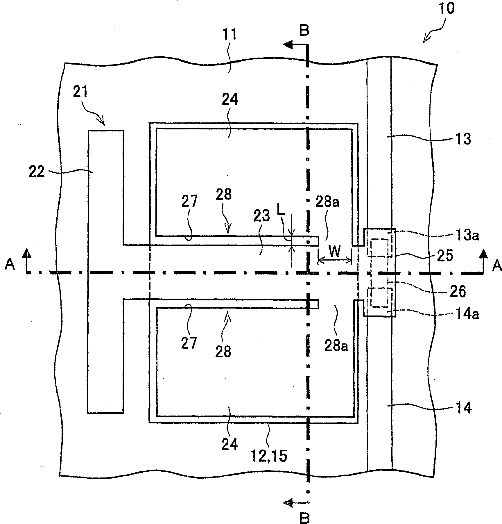
参照图1~图5说明本发明的一种实施方式。图1表示本实施方式的静电微继电器(静电微触点通断器)的概要。静电微继电器10具有:基座11、以及一部分被固定在基座11的上面、另一部分与基座11分开的致动器21。另外,对图中相同的部件标以相同的标号。此外,在附图中,为了使本发明容易理解,对所需要的部分强调而进行记载。因此,附图所示的静电微继电器10的各种尺寸不一定反映了实际的静电微继电器10的各种尺寸。An embodiment of the present invention will be described with reference to FIGS. 1 to 5 . FIG. 1 shows the outline of an electrostatic microrelay (electrostatic microcontact switch) according to this embodiment. The
基座11由派拉克斯玻璃(Pyrex,注册商标)等的玻璃基板构成。在基座11的上面,由金、铜、铝等的导体形成有固定电极12和两个信号线13、14。两个信号线13、14在同一直线上稍微分开而配置,信号线13、14的相对部分分别成为固定触点13a、14a。此外,在固定电极12上形成有绝缘膜15,以防止固定电极12和可动电极24之间的短路。The
致动器21由硅等的半导体基板构成,具有:支撑部22、梁部23、可动电极24以及可动触点部25。支撑部22竖立地设置在基座11的上面,用于支撑梁部23、可动电极24、以及可动触点部25。梁部23从支撑部22向侧方延伸,经由连接部28弹性地支撑可动电极24,同时弹性地支撑可动触点部25。在梁部23的末端设置了可动触点部25,在梁部23的两侧经由连接部28、28设有可动电极24、24。另外,在本实施方式中,连接部28的厚度与梁部23以及可动电极24的厚度相同。The
可动电极24、24被设在与基座11的固定电极12相对的位置上。在本实施方式中,在可动电极24、24和梁部23之间的连接部28上,从支撑部22侧开始形成有狭缝27、27。从而,可动电极24、24和梁部23在可动触点部25侧是连接的。The
可动触点部25设置在与从固定触点13a到固定触点14a为止的区域相对的位置上.此外,在可动触点部25的下面形成了绝缘膜(未图示),在该绝缘膜上设有由导体构成的可动触点26.可动触点26与各固定触点13a、14a相对,通过与两个固定触点13a、14a闭合,将信号线13、14互相电连接.The
这样,本实施方式的静电微继电器10构成了可动触点26与两处的固定触点13a、14a接触或分离的双断结构。此外,由于本实施方式中的致动器21从一侧支撑可动触点部25,所以称为‘悬臂型(cantilever型)致动器’。In this way, the
图2(a)、(b)表示在固定电极12和可动电极24之间未施加电压的状态。在该情况下,如图所示,可动触点26和固定触点13a、14a分开,使信号线13、14互相电分离。2( a ), ( b ) show a state where no voltage is applied between the fixed
图3(a)、(b)表示在固定电极12和可动电极24之间施加了电压的状态。在该情况下,如图所示,通过由上述电压的施加而产生的静电引力,可动电极24向固定电极12侧驱动。由此,可动触点26和固定触点13a、14a接触,将信号线13、14互相电连接。3( a ), ( b ) show a state where a voltage is applied between the fixed
在本实施方式中,梁部23和可动电极24、24在可动触点部25侧是连接的,在支撑部22侧通过狭缝27而分开。由此,如图3(a)、(b)所示,可动电极24、24在除了可动触点部25侧的大部分上,隔着绝缘膜15与固定电极12接合。在该情况下,可动电极24和固定电极12间的静电引力与可动电极24和固定电极12之间的距离的平方成反比,因此显著增大。由此,即使增大梁部23的弹性常数,也可以增大提供给可动触点部25的接触力,并可以稳定可动触点26和固定触点13a、14a之间的接触电阻。In the present embodiment, the
接着,如果解除固定电极12和可动电极24之间的电压,则静电引力消失,致动器21通过梁部23及可动电极24的复原力而返回到图2(a)、(b)所示的原始位置上。在本实施方式中,如上所述,由于可以增大梁部23的弹性常数,所以可以增大梁部23提供给可动触点部25的回复力,可以防止可动触点26和固定触点13a、14a之间的附着。Next, when the voltage between the fixed
接着,研究本实施方式中的可动电极24的各种特性。由电压的施加产生的可动电极24的位移量取决于连接梁部23和可动电极24的连接部28的弹性常数。连接部28的弹性常数k由下式表示。Next, various characteristics of the
k∝W×H3/L3…(1)k∝W×H3/L3…(1)
这里,W是在连接部28中,连接可动电极24和梁部23的实际连接部分28a的长度,L是实际连接部分28a中的可动电极24和梁部23之间的宽度,H是可动电极24的厚度。在图1中示出了记号W、L,图2(b)中示出了记号H。Here, W is the length of the
另外,作为表示为了将可动电极24充分地吸附到固定电极12上所需的施加电压的指标,有拉入(Pull in)电压。拉入电压是使可动平行平板电极的电极间距离为小于等于初期的2/3的电压。当拉入电压低时,将可动电极24的大部分与固定电极12接合所需的施加电压也降低。In addition, there is a pull-in voltage as an index indicating the applied voltage required to sufficiently attract the
上述的拉入(Pull in)电压Vpi用下式表示。The above-mentioned pull-in (Pull in) voltage Vpi is represented by the following formula.
Vpi=((8×k×d03)/(27×ε×S))1/2…(2)Vpi=((8×k×d03)/(27×ε×S))1/2…(2)
这里,d0是无电压施加时的电极间的距离,ε是电极间的介电常数,S是电极面积。Here, d0 is the distance between the electrodes when no voltage is applied, ε is the dielectric constant between the electrodes, and S is the area of the electrodes.
此外,电极间的静电引力Fele用下式表示。In addition, the electrostatic attractive force Fele between electrodes is represented by the following formula.
Fele=(C×Vs2)/(2×d)…(3)Fele=(C×Vs2)/(2×d)…(3)
这里,C是电容,Vs是施加电压,d是电极间的距离。Here, C is a capacitance, Vs is an applied voltage, and d is a distance between electrodes.
比较图1和图2(b)、图40和图41(b)时,可以理解的是:在本实施方式的静电微继电器10中,与现有的静电微继电器100相比,虽然宽度L和厚度H相等,但实际连接部分28a的长度W比现有的实际连接部分的长度、即现有的连接部118的长度W短.从而,根据上述式(1),本实施方式的连接部28与现有的连接部118相比,可以减小弹性常数.进而,根据上述式(2),可以在不增大可动电极24的尺寸的情况下降低拉入电压.When comparing Fig. 1 and Fig. 2(b), Fig. 40 and Fig. 41(b), it can be understood that in the
接着,参照图4以及图5说明电压的施加产生的可动电极24的动作。图4表示图1所示的本实施方式的静电微继电器10的要部。此外,图5(a)~(d)是沿图4所示的C-C线、即经由可动电极24到可动触点部25剖开的图,表示可动电极24通过静电引力移动的情况。Next, the operation of the
本实施方式的可动电极24的动作如下所述。即,在无电压施加时,可动电极24为图5(a)所示的配置。然后,在施加电压时,首先如该图5(b)所示,可动电极24的外侧由于静电引力而向固定电极12侧移位。此时,如上所述,连接部28的弹性常数小、挠曲量多,所以可动电极24的位移量大,末端部隔着绝缘膜15与固定电极12接合。The operation of the
由于可动电极24的位移量大,从而可动电极24和固定电极12之间的距离减小,根据上述式(3),静电引力增大。由此,如该图5(c)所示,可动电极24以及可动触点部25向基座11侧移动。此时,由于连接部28的挠曲量大,因此上述电极之间的距离的减少量大,静电引力的增大量大。因此,可动电极24以及可动触点部25的位移量大,可动电极24的一半隔着绝缘膜15与固定电极12接合,同时可动触点26与固定触点13a接触。Since the displacement amount of the
由于可动电极24向基座11侧移动,从而可动电极24和固定电极12之间的距离进一步减小,根据上述式(3),静电引力进一步增大。由此,如该图5(d)所示,可动电极24以及可动触点部25向基座11侧进一步移动。由此,可动电极24的大部分隔着绝缘膜15与固定电极12接合,所以作用于可动电极24的静电引力显著增大,可动触点26和固定触点13a之间的接触力增大,接触电阻稳定。Since the
从而,通过在维持回复力的同时减小连接部28的弹性常数,从而可以增大静电引力。由此,可以确保与以往同等的回复力并提高接触力。另外,由于在接触力与以往同等的情况下可以降低静电引力,所以可以降低施加电压,或缩小可动电极24的尺寸。Therefore, by reducing the elastic constant of the connecting
另外,在本实施方式中,在梁部23的两侧设有可动电极24、24,但如图4所示,也可以仅在梁部23的一侧设置可动电极24。但是,为了使可动触点部25在不相对于基座11倾斜的情况下移动,优选为在梁部23的两侧设置可动电极24、24。In addition, in this embodiment, the
(实施例1)(Example 1)
接着,参照图6~图9说明本实施方式的静电微继电器10的具体例。另外,以下,将梁部23的长度方向作为纵向,将宽度方向作为横向。在本实施例的静电微继电器10中,基座11由玻璃基板构成,固定电极12、信号线13、14由Au形成,致动器21由硅半导体基板构成,可动触点26由Au形成。Next, a specific example of the
此外,本实施例的静电微继电器10中的各种尺寸如下.即,在梁部23中,长度(纵向的长度)为450μm,宽度(横向的长度)为120μm.此外,可动电极24的长度为410μm,宽度为500μm.此外,连接部28的长度为与可动电极24相同的410μm,宽度为40μm.连接部28中、狭缝27的长度为310μm,实际连接部分28a的长度W为100μm.此外,梁部23、可动电极24、可动触点部25以及连接部28的厚度H为21.15μm.此外,在无电压施加时,固定电极12及可动电极24之间的距离为1.2μm,固定触点13a、14a以及可动触点26之间的距离为1.0μm.In addition, various dimensions in the
图6表示关于本实施例的静电微继电器10,施加了20V的电压的情况下的致动器21的位移量的仿真结果。在图示中,用等高线连接位移量相等的点,并用点的密度表示由可动电极24的轮廓和等高线包围的区域中的位移量的概要。即,没有点的区域表示位移量大致为零的状态,点的密度最高的区域表示可动电极24与固定电极12接合的状态。FIG. 6 shows simulation results of the displacement amount of the
参照图6,可以理解,本实施方式的可动电极24的位移量大,几乎都与固定电极12接合。从而,可以理解,通过固定电极12及可动电极24之间的静电引力,可动触点26按压固定触点13a、14a的力比以往大,所以接触力增大。Referring to FIG. 6 , it can be understood that the
接着,参照图7~图9更详细地研究本实施例以及比较例的接触力。另外,比较例是图40所示的现有的静电微继电器100,除了狭缝27外具有与本实施例的上述尺寸同样的尺寸。另外,为了使本实施例和比较例的回复力一致,在比较例的静电微继电器100中,将梁部113、可动电极114以及可动触点部115的厚度设为19.46μm。即,在本实施例的静电微继电器10中,增大了梁部23、可动电极24、可动触点部25以及连接部28的厚度H,以确保与以往相同程度的回复力。Next, the contact force of the present example and the comparative example will be examined in more detail with reference to FIGS. 7 to 9 . In addition, the comparative example is a conventional
图7是表示本实施例的静电微继电器10和比较例的静电微继电器100中的施加电压和接触力之间的关系的曲线图。参照该图,可以理解,本实施例的静电微继电器10在回复力与以往相同程度的情况下,接触力与以往相比显著地提高到9倍左右。FIG. 7 is a graph showing the relationship between the applied voltage and the contact force in the
此外,接触力变得比零大是表示固定触点13a、14a和可动触点26接触、静电微继电器10成为接通的状态。从而,参照图7,可以理解,在比较例中,在施加电压为17V处成为接通状态,相对于此,在本实施例中,在施加电压为15V处成为接通状态。即,可以理解本实施例的静电微继电器10在比以往低的施加电压下成为接通状态。In addition, when the contact force becomes larger than zero, it means that the fixed
此外,参照图7,施加电压为15V时的本实施例的接触力大于施加电压为20V时的比较例的接触力。从而,在可以维持与以往相同程度的接触力(0.21mN)的情况下,可以将施加电压从约20V到约15V减少约25%。这等价于使电极面积成为大约一半。其结果是,可以实现能够比以往小型化和/或低电压化的静电微继电器10。In addition, referring to FIG. 7 , the contact force of the present example when the applied voltage is 15V is greater than that of the comparative example when the applied voltage is 20V. Therefore, the applied voltage can be reduced by about 25% from about 20V to about 15V while maintaining the same level of contact force (0.21mN) as conventional. This is equivalent to making the electrode area approximately half. As a result, the
另外,如上述式(3)这样,静电引力与静电电容成正比,但本实施例中的静电电容为29.31pF,比较例中的静电电容为7.16pF。从而,可以理解本实施例的静电微继电器10与现有的静电微继电器100相比,在相同的施加电压下静电引力显著提高。In addition, as in the above formula (3), the electrostatic attraction is proportional to the electrostatic capacitance, but the electrostatic capacitance in the present example is 29.31 pF, and the electrostatic capacitance in the comparative example is 7.16 pF. Therefore, it can be understood that the electrostatic attractive force of the
图8以及图9分别以表格以及曲线图表示在本实施例的静电微继电器10中,狭缝27的长度和接触力之间的关系。参照图9的曲线图,可以理解,从狭缝27的长度为150μm的位置开始,接触力急剧地上升。从而,狭缝27的长度优选为大于等于150μm、即至少为可动电极24的长度的37%。FIG. 8 and FIG. 9 show the relationship between the length of the
进而,参照图9的曲线图,可以理解,在狭缝27的长度为250μm的情况下,接触力最大,此后接触力大致相同。从而,使狭缝27的长度为大于等于250μm、即至少为可动电极24的长度的60%在确保稳定的接触力上是更理想的。其中,考虑制造时的偏差或实际连接部分28a处的强度时,狭缝27的长度特别优选为可动电极24的长度的70~90%的280~370μm。Furthermore, referring to the graph of FIG. 9 , it can be understood that the contact force is maximum when the length of the
[实施方式2][Embodiment 2]
接着参照图10说明本发明的另一种实施方式.本实施方式的静电微继电器10与图1所示的静电微继电器10相比,其不同之处仅在于在信号线13、14的两侧设有固定电极12,以及在可动触点部25的两侧设有支撑部22、梁部23、可动电极24、以及连接部28,其它的结构是同样的.另外,对于与上述实施方式中所说明的结构具有同样的功能的结构标以同一标号,省略其说明.Next, another embodiment of the present invention is described with reference to FIG. 10. The
图10是表示本实施方式的静电微继电器10的概要的图。另外,图示的致动器21从两侧支撑可动触点部25,因此称为‘双支撑型致动器’。FIG. 10 is a diagram showing an outline of an
本实施方式的静电微继电器10可以起到与图1所示的静电微继电器10同样的作用效果。进而,本实施方式的静电微继电器10与图1所示的静电微继电器10相比,在信号线13、14的两侧需要载置固定电极12等的空间,但由于可以使可动触点部25相对于基座11维持大致平行状态,并向垂直方向移动,因此可以使可动触点26和固定触点13a、14a之间的接触稳定。此外,可以抑制接触部分的不均匀磨损。The
(实施例2)(Example 2)
接着,参照图11说明本实施方式的静电微继电器10的具体例。本实施例的静电微继电器10与图1所示的静电微继电器10的实施例相比,其不同点仅在于在信号线13、14的两测设有固定电极12,以及在可动触点部25的两侧设有支撑部22、梁部23、可动电极24、以及连接部28,构成要素的材质或各种尺寸是同样的。Next, a specific example of the
图11表示关于本实施例的静电微继电器10,施加了20V的电压的情况下的可动电极24的位移量的仿真结果。另外,图示的等高线或点表示与图6同样的意义。FIG. 11 shows simulation results of the displacement amount of the
参照图11,可以理解,本实施例的可动电极24的位移量大,几乎都与固定电极12接合。从而,可以理解,通过固定电极12及可动电极24之间的静电引力,使可动触点26按压固定触点13a、14a的力比以往大,所以接触力增大。Referring to FIG. 11 , it can be understood that the displacement of the
[实施方式3][Embodiment 3]
接着,参照图12~图19说明本发明的又一种实施方式。本实施方式的静电微继电器10与图1所示的静电微继电器10相比,其不同之处仅在于连接部28中的实际连接部分,其它的结构是同样的。另外,对于与上述实施方式中所说明的结构具有同样的功能的结构标以同一标号,省略其说明。Next, still another embodiment of the present invention will be described with reference to FIGS. 12 to 19 . Compared with the
图12是表示本实施方式的静电微继电器10的概要的图。如图所示,本实施方式的静电微继电器10与图1所示的静电微继电器10相比,连接部28中的实际连接部分28b中的材质和/或结构与梁部23及可动电极24中的材质和/或结构不同。由此,根据实际连接部分28b的材质和/或结构,可以容易地变更实际连接部分28b的宽度或厚度,所以实际连接部分28b的设计的自由度提高。FIG. 12 is a diagram showing an outline of an
另外,作为实际连接部分28b的结构例,可以举出将实际连接部分28b作为层叠膜的结构,或对实际连接部分28b填充导电物之后削为单层的结构。In addition, examples of the structure of the
接着,参照图13~图15说明上述结构的静电微继电器10的制造方法。Next, a method of manufacturing the
图13(a)、(b)表示基座11的制造步骤的一例.首先,如该图13(a)所示,准备派拉克斯玻璃(Pyrex,注册商标)等的玻璃基板11a.接着,如该图13(b)所示,在玻璃基板11a上形成金属膜,构图形成固定电极12以及信号线13、14.另外,也可以与此同时,构图形成其它的印刷配线以及连接用焊盘.然后,通过在固定电极12上形成绝缘膜15,完成基座11.另外,如果使用相对介电常数为3~4的氧化硅膜或相对介电常数为7~8的氮化硅膜作为绝缘膜15,则可以得到大的静电引力,增大接触力.Figure 13 (a), (b) shows an example of the manufacturing steps of the
图14(a)、(b)表示致动器21的制造步骤的一例。首先,如该图14(a)所示,准备SOI(Silicon On Insulator)晶片30。接着,如该图14(b)所示,例如,进行将氧化硅膜作为掩模的通过TMAH(Tetramethylammonium hydroxide,四甲基氢氧化铵)实现的湿式蚀刻,形成支撑部22。然后,形成绝缘膜以及金属膜,构图形成可动触点26。An example of the manufacturing steps of the
图15(a)~(c)表示基座11以及致动器21的连接步骤的一例。首先,如该图15(a)所示,通过阳极接合将SOI晶片30与基座11接合为一体。接着,如该图15(b)所示,用TMAH、KOH等的碱性蚀刻液将SOI晶片30的上面蚀刻到氧化硅(SiO2)膜31,使其变薄。进而,如该图15(c)所示,用氟类蚀刻液除去与连接部28的实际连接部分28b对应的区域以外的氧化硅膜31,从而露出梁部23、可动电极24以及可动触点部25。接着,进行使用了RIE(Reactive Ion Etching,反应离子蚀刻)等的干式蚀刻,形成狭缝27、27和各种切口部(未图示),完成静电微继电器10。15( a ) to ( c ) show an example of the connection procedure of the
从而,如图15(c)所示,通过图13~图15所示的制造方法制造出的连接部28的实际连接部分28b成为在与梁部23及可动电极24同样的硅层上形成了压缩应力膜的氧化硅膜31的层叠结构。Therefore, as shown in FIG. 15(c), the
接着,参照图16以及图17说明上述结构的静电微继电器10的另一种制造方法。另外,基座11的制造步骤与图13所示的制造步骤是同样的,所以省略其说明。Next, another manufacturing method of the
图16(a)~(c)表示致动器21的制造步骤的一例。首先,如该图16(a)所示,准备SOI晶片30。接着,如该图16(b)所示,从SOI晶片30的上面开始,例如,进行将氧化硅膜作为掩模的通过TMAH实现的湿式蚀刻,形成支撑部22。然后,如该图16(c)所示,形成绝缘膜以及金属膜,构图形成可动触点26。与此同时,在与连接部28的实际连接部分28b对应的区域中也构图形成金属膜。16( a ) to ( c ) show an example of the manufacturing steps of the
图17(a)、(b)表示基座11以及致动器21的连接步骤的一例。首先,如该图17(a)所示,通过阳极接合将SOI晶片30与基座11接合为一体。接着,如该图17(b)所示,用TMAH、KOH等的碱性蚀刻液将SOI晶片30的上面蚀刻到氧化硅膜31,使其变薄,进而用氟类蚀刻液除去氧化硅膜31而露出梁部23、可动电极24以及可动触点部25。接着,进行使用了RIE等的干式蚀刻,形成狭缝27、27和各种切口部(未图示),完成静电微继电器10。17( a ), ( b ) show an example of the connection procedure of the
从而,如图17(b)所示,通过图16以及图17所示的制造方法制造出的连接部28的实际连接部分28b成为由与梁部23及可动电极24同样的硅层和在基座11侧形成的金属膜32构成的层叠结构。Therefore, as shown in FIG. 17(b), the actual connecting
接着,参照图18以及图19说明上述结构的静电微继电器10的其它制造方法。另外,基座11的制造步骤与图13所示的制造步骤是同样的,所以省略其说明。Next, another manufacturing method of the
图18(a)~(c)表示致动器21的制造步骤的一例。首先,如该图18(a)所示,准备SOI晶片30。接着,如该图18(b)所示,从SOI晶片30的上面开始,例如,进行将氧化硅膜作为掩模的通过TMAH实现的湿式蚀刻,形成支撑部22。进而对与连接部28的实际连接部分28b对应的区域进行蚀刻,从而露出氧化硅膜31。然后,如该图18(c)所示,形成绝缘膜以及金属膜,构图形成可动触点26。与此同时,在与连接部28的实际连接部分28b对应的凹部中也构图形成金属膜33。18( a ) to ( c ) show an example of the manufacturing steps of the
图19(a)、(b)表示基座11以及致动器21的连接步骤的一例.首先,如该图19(a)所示,通过阳极接合将SOI晶片30与基座11接合为一体.接着,如该图19(b)所示,用TMAH、KOH等的碱性蚀刻液将SOI晶片30的上面蚀刻到氧化硅膜31,使其变薄,进而,用氟类蚀刻液除去氧化硅膜31,从而露出梁部23、可动电极24以及可动触点部25.接着,进行使用了RIE等的干式蚀刻,形成狭缝27、27和各种切口部(未图示),完成静电微继电器10.19(a), (b) show an example of the connection procedure of the
从而,如图19(b)所示,通过图18以及图19所示的制造方法制造出的连接部28的实际连接部分28b成为由材质与梁部23及可动电极24不同的金属膜33构成的单层结构。Therefore, as shown in FIG. 19( b ), the actual connecting
[实施方式4][Embodiment 4]
接着,参照图20说明本发明的又一种实施方式。本实施方式的静电微继电器10与图1所示的静电微继电器10相比,其不同之处仅在于将触点结构设为单断(single break)结构,其它的结构是同样的。另外,对于与上述实施方式中所说明的结构具有同样的功能的结构标以同一标号,省略其说明。Next, still another embodiment of the present invention will be described with reference to FIG. 20 . Compared with the
图20表示本实施方式的静电微继电器10的概要。如图所示,本实施方式的静电微继电器10与图1所示的静电微继电器10相比,基座11上的信号线13、14夹着固定电极12,与梁部23设在同一直线上。另外,信号线13中的与信号线14相对的部分为固定触点13a。FIG. 20 shows the outline of the
此外,在从致动器21的支撑部22的中央经由梁部23到可动触点部25为止的下表面上,隔着绝缘膜(未图示)形成有由导体构成的信号线35。信号线35与基座11的信号线14电连接,可动触点部25的下面部分、即与信号线13的固定触点13a的相对部分为可动触点35a。In addition, a
在上述结构的静电微继电器10中,在可动电极24和固定电极12间施加电压时,可动触点部25移动,从而可动触点35a和固定触点13a接触。由此,信号线13、14经由信号线35电连接。这样,在本实施方式中,是可动触点35a与一处的固定触点13a接触或分离的单断结构。本实施方式的静电微继电器10与图1所示的静电微继电器10相比,触点的数量少,因此提高了接触可靠性。In the
[实施方式5][Embodiment 5]
接着,参照图21~图25说明本发明的又一种实施方式。本实施方式的静电微继电器10与图1所示的静电微继电器10相比,不同之处仅为连接部28的结构,其它的结构是同样的。另外,对于与上述实施方式中所说明的结构具有同样的功能的结构标以同一标号,省略其说明。Next, still another embodiment of the present invention will be described with reference to FIGS. 21 to 25 . Compared with the
图21表示本实施方式的静电微继电器10的概要。如图所示,本实施方式的静电微继电器10与图1所示的静电微继电器10相比,不同点仅在于在可动电极24、24和梁部23之间的连接部28、28上形成有凹部50、50。FIG. 21 shows the outline of the
图22(a)、(b)表示在固定电极12和可动电极24之间未施加电压的状态。在该情况下,如图所示,可动触点26和固定触点13a、14a分开,使信号线13、14互相电分离。22( a ), ( b ) show a state where no voltage is applied between the fixed
图23(a)、(b)表示在固定电极12和可动电极24之间施加了电压的状态。在该情况下,如图所示,通过由上述电压的施加产生的静电引力,可动电极24向固定电极12侧驱动。由此,可动触点26和固定触点13a、14a接触,将信号线13、14互相电连接。23( a ) and ( b ) show a state where a voltage is applied between the fixed
在本实施方式中,在连接部28上形成有凹部50、50.由于凹部50比梁部23及可动电极24薄,所以弹性常数比以往小,容易挠曲.从而,如图23(a)、(b)所示,通过在凹部50、50中较大地挠曲,可动电极24、24在除了接近梁部23的区域之外的大部分区域中隔着绝缘膜15与固定电极12接合.在该情况下,可动电极24和固定电极12间的静电引力与可动电极24和固定电极12之间的距离的平方成反比,因此显著增大.由此,即使增大梁部23的弹性常数,仍可以增大提供给可动触点部25的接触力,可以使可动触点26和固定触点13a、14a之间的接触电阻稳定.In this embodiment, recesses 50, 50 are formed on the connecting
然后,如果解除固定电极12和可动电极24之间的电压,则静电引力消失,致动器21通过梁部23、可动电极24以及凹部50的复原力而返回到图22(a)、(b)所示的原始的位置上。Then, if the voltage between the fixed
接着,参照图24以及图25说明电压的施加所产生的可动电极24的动作。图24表示图21所示的本实施方式的静电微继电器10的要部。此外,图25(a)~(d)是沿图24所示的C-C线、即经由可动电极24到可动触点部25剖开的图,表示可动电极24通过静电引力而移动的情况。Next, the operation of the
本实施方式的可动电极24的动作如下。即,在无电压施加时,可动电极24成为图25(a)所示的配置。然后,在施加电压时,首先如该图25(b)所示,可动电极24由于静电引力而向固定电极12侧移位。此时,如上所述,本实施方式的凹部50的弹性常数比以往小,所以挠曲量大。因此,可动电极24的位移量大,可动电极24的末端隔着绝缘膜15与固定电极12接合。The
由于可动电极24的位移量大,可动电极24和固定电极12之间的距离减小,根据上述式(3),静电引力增大。由此,如该图25(c)所示,可动电极24以及可动触点部25向基座11侧移动。此时,由于本实施方式的凹部50的挠曲量大,因此上述电极之间的距离的减少量大,静电引力的增大量大。因此,可动电极24以及可动触点部25的位移量大,可动电极24的一半隔着绝缘体15与固定电极12接合,同时可动触点26与固定触点13a接触。Since the displacement amount of the
由于可动电极24向基座11侧移动,可动电极24和固定电极12之间的距离进一步减小,根据上述式(3),静电引力进一步增大。由此,如该图25(d)所示,可动电极24以及可动触点部25进一步向基座11侧移动。由此,可动电极24的大部分隔着绝缘膜15与固定电极12接合,所以作用于可动电极24的静电引力显著增大,可动触点26和固定触点13a之间的接触力增大,接触电阻稳定。As the
从而,通过在维持回复力的同时减小连接部28的弹性常数,从而可以增大静电引力。由此,可以确保与以往同等的回复力并提高接触力。另外,在接触力与以往同等的情况下可以降低静电引力,所以可以降低施加电压,或缩小可动电极24的尺寸。Therefore, by reducing the elastic constant of the connecting
另外,在本实施方式中,在梁部23的两侧设有可动电极24、24,但也可以如图24所示,仅在梁部23的一侧设置可动电极24。但是,为了使可动触点部25在不相对于基座11倾斜的情况下移动,优选为在梁部23的两侧设置可动电极24、24。In addition, in this embodiment, the
[实施方式6][Embodiment 6]
接着,参照图26说明本发明的另一种实施方式.本实施方式的静电微继电器10与图21所示的静电微继电器10相比,不同点仅在于在信号线13、14的两侧设有固定电极12,以及在可动触点部25的两侧设有支撑部22、梁部23、可动电极24以及连接部28,其它的结构是同样的.另外,对于与上述实施方式中所说明的结构具有同样的功能的结构标以同一标号,省略其说明.Next, another embodiment of the present invention will be described with reference to FIG. 26. Compared with the
图26表示本实施方式的静电微继电器10的概要。另外,图示的致动器21是从两侧支撑可动触点部25的双支撑型致动器。FIG. 26 shows the outline of the
本实施方式的静电微继电器10可以起到与图21所示的静电微继电器10同样的作用效果。进而,本实施方式的静电微继电器10与图21所示的静电微继电器10相比,在信号线13、14的两侧需要载置固定电极12等的空间,但由于可以使可动触点部25相对于基座11维持大致平行状态,并向垂直方向移动,因此可以使可动触点26和固定触点13a、14a之间的接触稳定。此外,可以抑制接触部分的不均匀磨损。The
[实施方式7][Embodiment 7]
接着,参照图27~图34说明本发明的另一种实施方式。本实施方式的静电微继电器10与图21所示的静电微继电器10相比,不同之处仅为连接部的结构,其它的结构是同样的。另外,对于与上述实施方式中所说明的结构具有同样的功能的结构标以同一标号,省略其说明。Next, another embodiment of the present invention will be described with reference to FIGS. 27 to 34 . Compared with the
图27(a)、(b)表示本实施方式的静电微继电器10的结构。如图所示,本实施方式的静电微继电器10与图21所示的静电微继电器10相比,梁部23和可动电极24、24之间的连接部51为梁部23或可动电极24延伸而成的、弹性常数比以往的连接部小的导体或半导体。由此,根据连接部51的材质和/或结构,可以容易地变更连接部51的宽度或厚度,所以连接部51的设计的自由度提高。另外,作为连接部51的结构例,可以举出将连接部51设为层叠膜的结构、或在对连接部51填充了导电物之后削为单层的结构。27(a), (b) show the structure of the
接着,参照图28~图30说明上述结构的静电微继电器10的制造方法。Next, a method of manufacturing the
图28(a)、(b)表示基座11的制造步骤的一例。首先,如该图28(a)所示,准备派拉克斯玻璃(Pyrex,注册商标)等的玻璃基板11a。接着,如该图28(b)所示,在玻璃基板11a上形成金属膜,构图形成固定电极12以及信号线13、14。另外,也可以与此同时,构图形成其它的印刷配线以及连接用焊盘。然后,通过在固定电极12上形成绝缘膜15,完成基座11。另外,如果使用相对介电常数为3~4的氧化硅膜或相对介电常数为7~8的氮化硅膜作为绝缘膜15,则可以得到大的静电引力,增大接触力。28( a ), ( b ) show an example of the manufacturing steps of the
图29(a)~(c)表示致动器21的制造步骤的一例。首先,如该图29(a)所示,准备SOI晶片30。接着,如该图29(b)所示,从SOI晶片30的上面起,例如,进行将氧化硅膜作为掩模的通过TMAH实现的湿式蚀刻,形成支撑部22。进而,对与连接部51对应的区域进行蚀刻,从而露出氧化硅膜31。然后,如该图29(c)所示,形成绝缘膜以及金属膜,构图形成可动触点26。与此同时,在与连接部51对应的区域中也构图形成金属膜60。29( a ) to ( c ) show an example of the manufacturing steps of the
图30(a)、(b)表示基座11以及致动器21的连接步骤的一例。首先,如该图30(a)所示,通过阳极接合将SOI晶片30与基座11接合为一体。接着,如该图30(b)所示,用TMAH、KOH等的碱性蚀刻液将SOI晶片30的上面蚀刻到氧化硅膜31,使其变薄,进而,用氟类蚀刻液除去氧化硅膜31,从而露出梁部23、可动电极24、可动触点部25以及连接部51。接着,进行使用了RIE等的干式蚀刻,形成各种切口部(未图示),完成静电微继电器10。30( a ), ( b ) show an example of the connection procedure of the
从而,如图30(b)所示,通过图28~图30所示的制造方法制造出的连接部51成为由材质与梁部23及可动电极24不同的金属膜60构成的单层结构。Therefore, as shown in FIG. 30(b), the connecting
接着,参照图31以及图32说明上述结构的静电微继电器10的另一种制造方法.另外,基座11的制造步骤与图28所示的制造步骤是同样的,所以省略其说明.Next, another manufacturing method of the
图31(a)、(b)表示致动器21的制造步骤的一例。首先,如该图31(a)所示,准备SOI晶片30。接着,如该图31(b)所示,例如,进行将氧化硅膜作为掩模的通过TMAH实现的湿式蚀刻,形成支撑部22。然后,形成绝缘膜以及金属膜,构图形成可动触点26。31( a ), ( b ) show an example of the manufacturing steps of the
图32(a)、(b)表示基座11以及致动器21的连接步骤的一例。首先,如该图32(a)所示,通过阳极接合将SOI晶片30与基座11接合为一体。接着,如该图32(b)所示,用TMAH、KOH等的碱性蚀刻液将SOI晶片30的上面蚀刻到氧化硅(SiO2)膜31,使其变薄,进而,用氟类蚀刻液除去与连接部51对应的区域以外的氧化硅膜31,从而露出梁部23、可动电极24以及可动触点部25。接着,进行使用了RIE等的干式蚀刻,形成各种切口部(未图示),完成静电微继电器10。32( a ), ( b ) show an example of the connection procedure of the
从而,如图32(b)所示,通过图31以及图32所示的制造方法制造出的连接部51成为在与梁部23及可动电极24同样的硅层上形成了压缩应力膜的氧化硅膜31的层叠结构。Therefore, as shown in FIG. 32(b), the connecting
接着,参照图33以及图34说明上述结构的静电微继电器10的另一种制造方法。另外,基座11的制造步骤与图28所示的制造步骤是同样的,所以省略其说明。Next, another manufacturing method of the
图33(a)、(b)表示致动器21的制造步骤的一例。首先,如该图33(a)所示,准备SOI晶片30。接着,如该图33(b)所示,从SOI晶片30的上面起,例如,进行将氧化硅膜作为掩模的通过TMAH实现的湿式蚀刻,形成支撑部22。然后,形成绝缘膜以及金属膜,构图形成可动触点26。与此同时,在与连接部51对应的区域中也构图形成作为拉伸应力膜的金属膜62。33( a ), ( b ) show an example of the manufacturing steps of the
图34(a)、(b)表示基座11以及致动器21的连接步骤的一例。首先,如该图34(a)所示,通过阳极接合将SOI晶片30与基座11接合为一体。接着,如该图34(b)所示,用TMAH、KOH等的碱性蚀刻液将SOI晶片30的上面蚀刻到氧化硅膜31,使其变薄,进而,用氟类蚀刻液除去氧化硅膜31,从而露出梁部23、可动电极24以及可动触点部25。接着,进行使用了RIE等的干式蚀刻,形成各种切口部(未图示),完成静电微继电器10。34( a ), ( b ) show an example of the connection procedure of the
从而,如图34(b)所示,通过图33以及图34所示的制造方法制造出的连接部51成为由与梁部23及可动电极24同样的硅层和在基座11侧形成的金属膜62构成的层叠结构。另外,也可以使用SiN等其它的拉伸应力膜来代替金属膜62。Therefore, as shown in FIG. 34(b), the connecting
[实施方式8][Embodiment 8]
接着,参照图35说明本发明的又一种实施方式。本实施方式的静电微继电器10与图21所示的静电微继电器10相比,其不同之处仅在于将触点结构设为单断结构,其它的结构是同样的。另外,对于与上述实施方式中所说明的结构具有同样的功能的结构标以同一标号,省略其说明。Next, still another embodiment of the present invention will be described with reference to FIG. 35 . Compared with the
图35表示本实施方式的静电微继电器10的概要。如图所示,本实施方式的静电微继电器10与图21所示的静电微继电器10相比,基座11上的信号线13、14夹着固定电极12,与梁部23设在同一直线上。另外,信号线13中的与信号线14相对的部分为固定触点13a。FIG. 35 shows the outline of the
此外,在从致动器21的支撑部22的中央经由梁部23到可动触点部25为止的下表面上,隔着绝缘膜(未图示)形成有由导体构成的信号线35.信号线35与基座11的信号线14电连接,可动触点部25的下面部分、即与信号线13的固定触点13a的相对部分成为可动触点35a.In addition, on the lower surface of the actuator 21 from the center of the supporting
在上述结构的静电微继电器10中,在可动电极24和固定电极12之间施加电压时,可动触点部25移动,从而可动触点35a和固定触点13a接触。由此,信号线13、14经由信号线35电连接。这样,在本实施方式中,是可动触点35a与一处的固定触点13a接触或分离的单断结构。本实施方式的静电微继电器10与图21所示的静电微继电器10相比,触点的数量少,因此提高了接触可靠性。In the
[实施方式9][Embodiment 9]
接着,参照图36说明本发明的又一种实施方式。图36表示本实施方式的无线通信机71的概略结构。在无线通信机71中,静电微继电器72连接在内部处理电路73和天线74之间。通过将静电微继电器72接通、断开,在内部处理电路73可通过天线74进行发送或接收的状态和不能发送或接收的状态之间进行切换。Next, still another embodiment of the present invention will be described with reference to FIG. 36 . FIG. 36 shows a schematic configuration of wireless communication device 71 according to this embodiment. In the wireless communication machine 71 , an
在本实施方式中,对于静电微继电器72利用了图1~图35所示的静电微继电器10。由此,在静电微继电器72中可以实现驱动电压的降低以及小型化,所以可以实现无线通信机71的低功率化以及小型化。In this embodiment, the
[实施方式10][Embodiment 10]
接着,参照图37说明本发明的又一种实施方式。图37表示本实施方式的计测器75的概略结构。在计测器75中,多个静电微继电器72分别连接在从一个内部处理电路76到多个测量对象体78的多个信号线77的中间。通过将各个静电微继电器72接通、断开,从而内部处理电路76可以切换要进行发送或接收的测量对象体78。Next, still another embodiment of the present invention will be described with reference to FIG. 37 . FIG. 37 shows a schematic configuration of a measuring device 75 according to this embodiment. In the measuring device 75 , a plurality of
在本实施方式中,对于静电微继电器72利用了图1~图35所示的静电微继电器10。由此,在静电微继电器72中可以实现驱动电压的降低以及小型化,所以可以实现计测器75的低功率化以及小型化。In this embodiment, the
[实施方式11][Embodiment 11]
接着,参照图38说明本发明的又一种实施方式。图38表示本实施方式的温度管理装置(温度传感器)81的概略结构。温度管理装置81例如安装在电源装置、控制设备等的需要对于温度的安全功能的装置(以下称为‘对象装置’)82中,用于管理对象装置82的温度。如图所示,温度管理装置81具有静电微继电器72,其用于基于对象装置82的温度来接通、断开向对象装置82的内部电路83的供电。Next, still another embodiment of the present invention will be described with reference to FIG. 38 . FIG. 38 shows a schematic configuration of a temperature management device (temperature sensor) 81 according to this embodiment. The temperature management device 81 is installed, for example, in a device (hereinafter referred to as 'target device') 82 that requires a temperature safety function such as a power supply device or a control device, and is used to manage the temperature of the target device 82 . As shown, the temperature management device 81 has an electrostatic micro-relay 72 for turning on and off the power supply to the internal circuit 83 of the subject device 82 based on the temperature of the subject device 82 .
例如,在对象装置82的使用极限为在大于等于100℃的温度下、不超过一小时的情况下,温度管理装置81计测对象装置82的温度,如果检测到对象装置82在大于等于100℃的温度下工作了一小时,则温度管理装置81内的静电微继电器72断开对内部装置82的内部电路83的供电。For example, when the service limit of the target device 82 is at a temperature of 100° C. After working for one hour at a temperature of 100, the
在本实施方式中,对于静电微继电器72利用了图1~图35所示的静电微继电器10。由此,在静电微继电器72中可以实现驱动电压的降低以及小型化,所以可以实现温度管理装置81的低功率化以及小型化。In this embodiment, the
[实施方式12][Embodiment 12]
接着,参照图39说明本发明的另一个实施方式.图39表示本实施方式的便携信息终端85的要部结构.在便携信息终端85中,利用了两个静电微继电器72a、72b.一个静电微继电器72a作用为在内部天线86和外部天线87之间进行切换,另一个静电微继电器72b在发送电路侧的功率放大器88和接收电路侧的低噪声放大器89之间切换信号流.Next, another embodiment of the present invention will be described with reference to FIG. 39. FIG. 39 shows the main structure of the portable information terminal 85 of this embodiment. In the portable information terminal 85, two electrostatic microrelays 72a, 72b are used. One electrostatic microrelay The micro-relay 72a is used to switch between the internal antenna 86 and the external antenna 87, and another electrostatic micro-relay 72b switches the signal flow between the power amplifier 88 on the transmitting circuit side and the low noise amplifier 89 on the receiving circuit side.
在本实施方式中,对于静电微继电器72a、72b利用了图1~图35所示的静电微继电器10。由此,在静电微继电器72a、72b中可以实现驱动电压的降低以及小型化,所以可以实现便携信息终端85的低功率化以及小型化。In this embodiment, the
如上所述,本实施方式的静电微继电器10可以确保与以往同等的回复力,并实现接触力的提高、施加电压的降低、和/或电极尺寸的缩小,所以例如通过在无线通信机、计测器、温度管理装置、便携信息终端等的各种装置中采用本实施方式的静电微继电器10,可以实现装置的低功率化以及小型化。As described above, the
本发明不限于上述的各种实施方式,在权利要求的范围内可进行各种变更,对于组合不同实施方式中分别公开的技术手段而得到的实施方式,也包含于本发明的技术范围内。The present invention is not limited to the various embodiments described above, and various changes can be made within the scope of the claims. Embodiments obtained by combining technical means disclosed in different embodiments are also included in the technical scope of the present invention.
例如,在上述实施方式中,说明了静电微继电器,但可以对于静电微开关等的通过静电引力使触点之间接触或分离而对电路进行通断的任意的静电微触点通断器应用本发明。For example, in the above-mentioned embodiment, the electrostatic micro-relay was described, but it can be applied to any electrostatic micro-contact circuit-breaker that contacts or separates contacts by electrostatic attraction, such as an electrostatic micro-switch. this invention.
此外,上述实施方式中,使可动触点部25的宽度比梁部23的宽度宽,但这是为了强调可动触点部25和梁部23之间的不同。从而,也可以使可动触点部25的宽度与梁部23的宽度相等,还可以在梁部23的宽度以下。In addition, in the above-described embodiment, the width of the
此外,在上述实施方式中,梁部23的大部分与固定电极12相对,在梁部23和固定电极12之间施加电压时,由于静电引力而向固定电极12侧驱动。从而,在梁部23中与固定电极12相对的部分具有作为可动电极24的功能。Furthermore, in the above embodiment, most of the
如上所述,由于本发明的静电微触点通断器可以确保与以往同等的回复力,并实现接触力的提高、施加电压的降低、和/或电极尺寸的缩小,所以也可以应用于要求低功率化以及小型化的其它的MEMS元件。As mentioned above, since the electrostatic micro-contact switch of the present invention can ensure the same restoring force as before, and realize the improvement of the contact force, the reduction of the applied voltage, and/or the reduction of the electrode size, it can also be applied to the requirements Other MEMS components for low power and miniaturization.
Claims (11)
Applications Claiming Priority (6)
| Application Number | Priority Date | Filing Date | Title |
|---|---|---|---|
| JP2005071729 | 2005-03-14 | ||
| JP2005071729 | 2005-03-14 | ||
| JP2005-071729 | 2005-03-14 | ||
| JP2006-016973 | 2006-01-25 | ||
| JP2006016973A JP4792994B2 (en) | 2005-03-14 | 2006-01-25 | Electrostatic micro contact switch, method for manufacturing the same, and apparatus using electrostatic micro contact switch |
| JP2006016973 | 2006-01-25 |
Publications (2)
| Publication Number | Publication Date |
|---|---|
| CN1848344A CN1848344A (en) | 2006-10-18 |
| CN1848344B true CN1848344B (en) | 2010-05-12 |
Family
ID=36570501
Family Applications (1)
| Application Number | Title | Priority Date | Filing Date |
|---|---|---|---|
| CN2006100648109A Expired - Fee Related CN1848344B (en) | 2005-03-14 | 2006-03-14 | Electrostatic micro-contact circuit breaker, manufacturing method thereof, and device using the same |
Country Status (8)
| Country | Link |
|---|---|
| US (1) | US7463126B2 (en) |
| EP (1) | EP1703532B1 (en) |
| JP (1) | JP4792994B2 (en) |
| KR (1) | KR100799454B1 (en) |
| CN (1) | CN1848344B (en) |
| AT (1) | ATE375000T1 (en) |
| DE (1) | DE602006000135T2 (en) |
| TW (1) | TWI300233B (en) |
Families Citing this family (11)
| Publication number | Priority date | Publication date | Assignee | Title |
|---|---|---|---|---|
| KR100601533B1 (en) * | 2004-07-28 | 2006-07-19 | 삼성에스디아이 주식회사 | Secondary protection element for secondary battery |
| FR2876995B1 (en) * | 2004-10-26 | 2007-05-04 | Commissariat Energie Atomique | MICROSYSTEM COMPRISING A DEFORMABLE BRIDGE |
| JP2006269127A (en) * | 2005-03-22 | 2006-10-05 | Toshiba Corp | Micromachine switch and electronic equipment |
| DE102007013102A1 (en) * | 2007-03-14 | 2008-09-18 | Fraunhofer-Gesellschaft zur Förderung der angewandten Forschung e.V. | Micromechanical switch device with mechanical power amplification |
| JP4970150B2 (en) * | 2007-06-01 | 2012-07-04 | 株式会社東芝 | Semiconductor device |
| JP2009021227A (en) * | 2007-06-14 | 2009-01-29 | Panasonic Corp | Electromechanical switch, filter using the same, and communication device |
| US8138859B2 (en) * | 2008-04-21 | 2012-03-20 | Formfactor, Inc. | Switch for use in microelectromechanical systems (MEMS) and MEMS devices incorporating same |
| US8779886B2 (en) * | 2009-11-30 | 2014-07-15 | General Electric Company | Switch structures |
| KR101914186B1 (en) | 2010-11-10 | 2018-12-28 | 타이코 일렉트로닉스 저팬 지.케이. | Contact structure |
| US9251984B2 (en) * | 2012-12-27 | 2016-02-02 | Intel Corporation | Hybrid radio frequency component |
| CN107749373B (en) * | 2017-10-24 | 2019-06-14 | 上海交通大学 | A large controllable stroke micro-actuator |
Citations (2)
| Publication number | Priority date | Publication date | Assignee | Title |
|---|---|---|---|---|
| US5278368A (en) * | 1991-06-24 | 1994-01-11 | Matsushita Elec. Works, Ltd | Electrostatic relay |
| US6115231A (en) * | 1997-11-25 | 2000-09-05 | Tdk Corporation | Electrostatic relay |
Family Cites Families (13)
| Publication number | Priority date | Publication date | Assignee | Title |
|---|---|---|---|---|
| DE4205029C1 (en) | 1992-02-19 | 1993-02-11 | Siemens Ag, 8000 Muenchen, De | Micro-mechanical electrostatic relay - has tongue-shaped armature etched from surface of silicon@ substrate |
| DE4205340C1 (en) * | 1992-02-21 | 1993-08-05 | Siemens Ag, 8000 Muenchen, De | Micro-mechanical electrostatic relay with parallel electrodes - has frame shaped armature substrate with armature contacts above base electrode contacts on base substrate |
| JP2900861B2 (en) * | 1995-10-05 | 1999-06-02 | オムロン株式会社 | Movable piece block |
| JP3493974B2 (en) | 1997-10-01 | 2004-02-03 | オムロン株式会社 | Electrostatic micro relay |
| JP3393467B2 (en) | 1997-10-27 | 2003-04-07 | オムロン株式会社 | Electrostatic micro relay |
| DE19823690C1 (en) * | 1998-05-27 | 2000-01-05 | Siemens Ag | Micromechanical electrostatic relay |
| JP3796988B2 (en) * | 1998-11-26 | 2006-07-12 | オムロン株式会社 | Electrostatic micro relay |
| JP2000243202A (en) * | 1999-02-22 | 2000-09-08 | Omron Corp | Micro-relay |
| JP2000317897A (en) * | 1999-02-23 | 2000-11-21 | Matsushita Electric Works Ltd | Heat insulating structure, semiconductor microactuator using the same, semiconductor microvalve, and semiconductor microrelay |
| KR100364726B1 (en) * | 2000-05-01 | 2002-12-16 | 엘지전자 주식회사 | micro switch and method for fabricating the same |
| US6768403B2 (en) * | 2002-03-12 | 2004-07-27 | Hrl Laboratories, Llc | Torsion spring for electro-mechanical switches and a cantilever-type RF micro-electromechanical switch incorporating the torsion spring |
| KR100519749B1 (en) * | 2001-05-10 | 2005-10-07 | 삼성전자주식회사 | Micro Electro Mechanical System switch comprising single anchor |
| JP4447940B2 (en) | 2004-02-27 | 2010-04-07 | 富士通株式会社 | Microswitching device manufacturing method and microswitching device |
-
2006
- 2006-01-25 JP JP2006016973A patent/JP4792994B2/en not_active Expired - Fee Related
- 2006-02-21 KR KR1020060016569A patent/KR100799454B1/en not_active Expired - Fee Related
- 2006-03-13 TW TW095108431A patent/TWI300233B/en not_active IP Right Cessation
- 2006-03-14 EP EP06111126A patent/EP1703532B1/en not_active Not-in-force
- 2006-03-14 CN CN2006100648109A patent/CN1848344B/en not_active Expired - Fee Related
- 2006-03-14 AT AT06111126T patent/ATE375000T1/en not_active IP Right Cessation
- 2006-03-14 DE DE602006000135T patent/DE602006000135T2/en active Active
- 2006-03-14 US US11/375,518 patent/US7463126B2/en not_active Expired - Fee Related
Patent Citations (2)
| Publication number | Priority date | Publication date | Assignee | Title |
|---|---|---|---|---|
| US5278368A (en) * | 1991-06-24 | 1994-01-11 | Matsushita Elec. Works, Ltd | Electrostatic relay |
| US6115231A (en) * | 1997-11-25 | 2000-09-05 | Tdk Corporation | Electrostatic relay |
Also Published As
| Publication number | Publication date |
|---|---|
| CN1848344A (en) | 2006-10-18 |
| US20060208837A1 (en) | 2006-09-21 |
| TWI300233B (en) | 2008-08-21 |
| TW200703399A (en) | 2007-01-16 |
| KR100799454B1 (en) | 2008-01-30 |
| DE602006000135T2 (en) | 2008-07-10 |
| EP1703532A1 (en) | 2006-09-20 |
| JP2006294591A (en) | 2006-10-26 |
| JP4792994B2 (en) | 2011-10-12 |
| DE602006000135D1 (en) | 2007-11-15 |
| KR20060100928A (en) | 2006-09-21 |
| ATE375000T1 (en) | 2007-10-15 |
| US7463126B2 (en) | 2008-12-09 |
| EP1703532B1 (en) | 2007-10-03 |
Similar Documents
| Publication | Publication Date | Title |
|---|---|---|
| JP5449756B2 (en) | MEMS switch with conductive mechanical stopper | |
| US6621135B1 (en) | Microrelays and microrelay fabrication and operating methods | |
| JP3918559B2 (en) | Electrostatic relay and communication equipment using the relay | |
| US7978045B2 (en) | Multi-actuation MEMS switch | |
| CN1848344B (en) | Electrostatic micro-contact circuit breaker, manufacturing method thereof, and device using the same | |
| JP2007159389A (en) | Piezoelectric RF-MEMS element and manufacturing method thereof | |
| JP2007535797A (en) | Beam for micromachine technology (MEMS) switches | |
| CN102290289B (en) | Electrostatically actuated micro-mechanical switching device | |
| CN100555499C (en) | Downward type MEMS switch and manufacturing method thereof | |
| KR100516278B1 (en) | Contact switch and apparatus provided with contact switch | |
| JP2004127871A (en) | Micro relay and method of manufacturing micro relay | |
| KR20110062583A (en) | High frequency capacitive switch and its manufacturing method | |
| JPWO2005015595A1 (en) | Microswitching element and method for manufacturing the same | |
| JP2006269127A (en) | Micromachine switch and electronic equipment | |
| EP1426992A2 (en) | Electrostatic mems switch | |
| JP4443438B2 (en) | Electromechanical switch | |
| KR100493532B1 (en) | Electrostatic bi-directional microelectromechanical actuator | |
| CN119706735B (en) | Micromachine switch manufacturing method and micromachine switch | |
| KR100636351B1 (en) | Electrostatic force driven RF MEMS switch and its manufacturing method | |
| JP2004281412A (en) | Electrostatic micro relay | |
| JP2006164989A (en) | Electrostatic micro relay | |
| JP2004071482A (en) | Micro relay |
Legal Events
| Date | Code | Title | Description |
|---|---|---|---|
| C06 | Publication | ||
| PB01 | Publication | ||
| C10 | Entry into substantive examination | ||
| SE01 | Entry into force of request for substantive examination | ||
| C14 | Grant of patent or utility model | ||
| GR01 | Patent grant | ||
| CF01 | Termination of patent right due to non-payment of annual fee | ||
| CF01 | Termination of patent right due to non-payment of annual fee |
Granted publication date: 20100512 Termination date: 20190314 |