CN1790757A - Light emitting device and method for fabricating the same - Google Patents
Light emitting device and method for fabricating the same Download PDFInfo
- Publication number
- CN1790757A CN1790757A CNA2005101156357A CN200510115635A CN1790757A CN 1790757 A CN1790757 A CN 1790757A CN A2005101156357 A CNA2005101156357 A CN A2005101156357A CN 200510115635 A CN200510115635 A CN 200510115635A CN 1790757 A CN1790757 A CN 1790757A
- Authority
- CN
- China
- Prior art keywords
- layer
- devices
- film
- light emitting
- emitting device
- Prior art date
- Legal status (The legal status is an assumption and is not a legal conclusion. Google has not performed a legal analysis and makes no representation as to the accuracy of the status listed.)
- Pending
Links
- 238000000034 method Methods 0.000 title claims abstract description 50
- 229910052751 metal Inorganic materials 0.000 claims abstract description 117
- 239000002184 metal Substances 0.000 claims abstract description 117
- 239000010408 film Substances 0.000 claims abstract description 66
- 239000010409 thin film Substances 0.000 claims abstract description 35
- 238000004519 manufacturing process Methods 0.000 claims abstract description 21
- 238000000926 separation method Methods 0.000 claims abstract description 8
- 239000000758 substrate Substances 0.000 claims description 41
- 229910002601 GaN Inorganic materials 0.000 claims description 37
- 238000002161 passivation Methods 0.000 claims description 35
- 229910052594 sapphire Inorganic materials 0.000 claims description 18
- 239000010980 sapphire Substances 0.000 claims description 18
- 239000004065 semiconductor Substances 0.000 claims description 18
- 238000005476 soldering Methods 0.000 claims description 18
- 238000003466 welding Methods 0.000 claims description 18
- JMASRVWKEDWRBT-UHFFFAOYSA-N Gallium nitride Chemical compound [Ga]#N JMASRVWKEDWRBT-UHFFFAOYSA-N 0.000 claims description 15
- 238000005530 etching Methods 0.000 claims description 10
- 229910052737 gold Inorganic materials 0.000 claims description 5
- 229910052782 aluminium Inorganic materials 0.000 claims description 4
- 229910052802 copper Inorganic materials 0.000 claims description 4
- 229910045601 alloy Inorganic materials 0.000 claims description 2
- 239000000956 alloy Substances 0.000 claims description 2
- 229910052759 nickel Inorganic materials 0.000 claims description 2
- 229910052763 palladium Inorganic materials 0.000 claims description 2
- 229910052703 rhodium Inorganic materials 0.000 claims description 2
- 229910052709 silver Inorganic materials 0.000 claims description 2
- 229910000679 solder Inorganic materials 0.000 claims description 2
- 229910018072 Al 2 O 3 Inorganic materials 0.000 claims 1
- -1 Si 3 N 4 Inorganic materials 0.000 claims 1
- 229910004541 SiN Inorganic materials 0.000 claims 1
- 229910004298 SiO 2 Inorganic materials 0.000 claims 1
- 229910010413 TiO 2 Inorganic materials 0.000 claims 1
- 238000000151 deposition Methods 0.000 claims 1
- 238000007747 plating Methods 0.000 claims 1
- 230000017525 heat dissipation Effects 0.000 abstract description 5
- 230000003287 optical effect Effects 0.000 abstract description 4
- 150000002739 metals Chemical class 0.000 abstract description 2
- 239000010410 layer Substances 0.000 description 170
- 239000000463 material Substances 0.000 description 17
- 238000005520 cutting process Methods 0.000 description 7
- 239000010931 gold Substances 0.000 description 7
- 239000010949 copper Substances 0.000 description 5
- JBRZTFJDHDCESZ-UHFFFAOYSA-N AsGa Chemical compound [As]#[Ga] JBRZTFJDHDCESZ-UHFFFAOYSA-N 0.000 description 4
- 229910052581 Si3N4 Inorganic materials 0.000 description 4
- VYPSYNLAJGMNEJ-UHFFFAOYSA-N Silicium dioxide Chemical compound O=[Si]=O VYPSYNLAJGMNEJ-UHFFFAOYSA-N 0.000 description 4
- HQVNEWCFYHHQES-UHFFFAOYSA-N silicon nitride Chemical compound N12[Si]34N5[Si]62N3[Si]51N64 HQVNEWCFYHHQES-UHFFFAOYSA-N 0.000 description 4
- RYGMFSIKBFXOCR-UHFFFAOYSA-N Copper Chemical compound [Cu] RYGMFSIKBFXOCR-UHFFFAOYSA-N 0.000 description 3
- 229910001218 Gallium arsenide Inorganic materials 0.000 description 3
- 239000000853 adhesive Substances 0.000 description 3
- 230000001070 adhesive effect Effects 0.000 description 3
- XAGFODPZIPBFFR-UHFFFAOYSA-N aluminium Chemical compound [Al] XAGFODPZIPBFFR-UHFFFAOYSA-N 0.000 description 3
- TWNQGVIAIRXVLR-UHFFFAOYSA-N oxo(oxoalumanyloxy)alumane Chemical compound O=[Al]O[Al]=O TWNQGVIAIRXVLR-UHFFFAOYSA-N 0.000 description 3
- BASFCYQUMIYNBI-UHFFFAOYSA-N platinum Chemical compound [Pt] BASFCYQUMIYNBI-UHFFFAOYSA-N 0.000 description 3
- 239000012790 adhesive layer Substances 0.000 description 2
- 239000011651 chromium Substances 0.000 description 2
- PCHJSUWPFVWCPO-UHFFFAOYSA-N gold Chemical compound [Au] PCHJSUWPFVWCPO-UHFFFAOYSA-N 0.000 description 2
- 238000002844 melting Methods 0.000 description 2
- 230000008018 melting Effects 0.000 description 2
- 238000012986 modification Methods 0.000 description 2
- 230000004048 modification Effects 0.000 description 2
- BPUBBGLMJRNUCC-UHFFFAOYSA-N oxygen(2-);tantalum(5+) Chemical compound [O-2].[O-2].[O-2].[O-2].[O-2].[Ta+5].[Ta+5] BPUBBGLMJRNUCC-UHFFFAOYSA-N 0.000 description 2
- 239000010948 rhodium Substances 0.000 description 2
- 235000012239 silicon dioxide Nutrition 0.000 description 2
- 239000000377 silicon dioxide Substances 0.000 description 2
- 229910001936 tantalum oxide Inorganic materials 0.000 description 2
- 239000010936 titanium Substances 0.000 description 2
- VYZAMTAEIAYCRO-UHFFFAOYSA-N Chromium Chemical compound [Cr] VYZAMTAEIAYCRO-UHFFFAOYSA-N 0.000 description 1
- 239000004642 Polyimide Substances 0.000 description 1
- XUIMIQQOPSSXEZ-UHFFFAOYSA-N Silicon Chemical compound [Si] XUIMIQQOPSSXEZ-UHFFFAOYSA-N 0.000 description 1
- BQCADISMDOOEFD-UHFFFAOYSA-N Silver Chemical compound [Ag] BQCADISMDOOEFD-UHFFFAOYSA-N 0.000 description 1
- GWEVSGVZZGPLCZ-UHFFFAOYSA-N Titan oxide Chemical compound O=[Ti]=O GWEVSGVZZGPLCZ-UHFFFAOYSA-N 0.000 description 1
- RTAQQCXQSZGOHL-UHFFFAOYSA-N Titanium Chemical compound [Ti] RTAQQCXQSZGOHL-UHFFFAOYSA-N 0.000 description 1
- 229910052804 chromium Inorganic materials 0.000 description 1
- 238000004140 cleaning Methods 0.000 description 1
- 238000007796 conventional method Methods 0.000 description 1
- 238000010586 diagram Methods 0.000 description 1
- 239000003822 epoxy resin Substances 0.000 description 1
- 239000012528 membrane Substances 0.000 description 1
- 229910052697 platinum Inorganic materials 0.000 description 1
- 229920000647 polyepoxide Polymers 0.000 description 1
- 229920001721 polyimide Polymers 0.000 description 1
- 229920001296 polysiloxane Polymers 0.000 description 1
- 239000011148 porous material Substances 0.000 description 1
- 238000003672 processing method Methods 0.000 description 1
- 229920005989 resin Polymers 0.000 description 1
- 239000011347 resin Substances 0.000 description 1
- MHOVAHRLVXNVSD-UHFFFAOYSA-N rhodium atom Chemical compound [Rh] MHOVAHRLVXNVSD-UHFFFAOYSA-N 0.000 description 1
- 229910052710 silicon Inorganic materials 0.000 description 1
- 239000010703 silicon Substances 0.000 description 1
- 239000004332 silver Substances 0.000 description 1
- 229910052715 tantalum Inorganic materials 0.000 description 1
- GUVRBAGPIYLISA-UHFFFAOYSA-N tantalum atom Chemical compound [Ta] GUVRBAGPIYLISA-UHFFFAOYSA-N 0.000 description 1
- XGZGDYQRJKMWNM-UHFFFAOYSA-N tantalum tungsten Chemical compound [Ta][W][Ta] XGZGDYQRJKMWNM-UHFFFAOYSA-N 0.000 description 1
- 229910052719 titanium Inorganic materials 0.000 description 1
- MAKDTFFYCIMFQP-UHFFFAOYSA-N titanium tungsten Chemical compound [Ti].[W] MAKDTFFYCIMFQP-UHFFFAOYSA-N 0.000 description 1
Images


Classifications
-
- H—ELECTRICITY
- H10—SEMICONDUCTOR DEVICES; ELECTRIC SOLID-STATE DEVICES NOT OTHERWISE PROVIDED FOR
- H10H—INORGANIC LIGHT-EMITTING SEMICONDUCTOR DEVICES HAVING POTENTIAL BARRIERS
- H10H20/00—Individual inorganic light-emitting semiconductor devices having potential barriers, e.g. light-emitting diodes [LED]
- H10H20/80—Constructional details
- H10H20/85—Packages
- H10H20/858—Means for heat extraction or cooling
-
- H—ELECTRICITY
- H10—SEMICONDUCTOR DEVICES; ELECTRIC SOLID-STATE DEVICES NOT OTHERWISE PROVIDED FOR
- H10H—INORGANIC LIGHT-EMITTING SEMICONDUCTOR DEVICES HAVING POTENTIAL BARRIERS
- H10H20/00—Individual inorganic light-emitting semiconductor devices having potential barriers, e.g. light-emitting diodes [LED]
- H10H20/01—Manufacture or treatment
- H10H20/011—Manufacture or treatment of bodies, e.g. forming semiconductor layers
- H10H20/018—Bonding of wafers
-
- H—ELECTRICITY
- H10—SEMICONDUCTOR DEVICES; ELECTRIC SOLID-STATE DEVICES NOT OTHERWISE PROVIDED FOR
- H10H—INORGANIC LIGHT-EMITTING SEMICONDUCTOR DEVICES HAVING POTENTIAL BARRIERS
- H10H20/00—Individual inorganic light-emitting semiconductor devices having potential barriers, e.g. light-emitting diodes [LED]
- H10H20/80—Constructional details
- H10H20/81—Bodies
- H10H20/819—Bodies characterised by their shape, e.g. curved or truncated substrates
-
- H—ELECTRICITY
- H10—SEMICONDUCTOR DEVICES; ELECTRIC SOLID-STATE DEVICES NOT OTHERWISE PROVIDED FOR
- H10H—INORGANIC LIGHT-EMITTING SEMICONDUCTOR DEVICES HAVING POTENTIAL BARRIERS
- H10H20/00—Individual inorganic light-emitting semiconductor devices having potential barriers, e.g. light-emitting diodes [LED]
- H10H20/80—Constructional details
- H10H20/84—Coatings, e.g. passivation layers or antireflective coatings
- H10H20/841—Reflective coatings, e.g. dielectric Bragg reflectors
-
- H—ELECTRICITY
- H10—SEMICONDUCTOR DEVICES; ELECTRIC SOLID-STATE DEVICES NOT OTHERWISE PROVIDED FOR
- H10H—INORGANIC LIGHT-EMITTING SEMICONDUCTOR DEVICES HAVING POTENTIAL BARRIERS
- H10H20/00—Individual inorganic light-emitting semiconductor devices having potential barriers, e.g. light-emitting diodes [LED]
- H10H20/01—Manufacture or treatment
- H10H20/036—Manufacture or treatment of packages
- H10H20/0365—Manufacture or treatment of packages of means for heat extraction or cooling
Landscapes
- Led Devices (AREA)
- Heating, Cooling, Or Curing Plastics Or The Like In General (AREA)
- Semiconductor Lasers (AREA)
Abstract
本发明的发光器件及其制造方法的优点在于,由于LLO(激光剥离)处理中使用由生长方法得到的厚金属膜,空隙的发生率因金属之间的紧密结合而显著降低,从而可以降低裂纹的发生率。另外,本发明的优点在于,用金属填充在由器件分离处理形成的沟槽区中,从而保护了器件并确保了良好的散热。本发明进一步的优点在于,反射膜形成于器件形成薄膜层的倾斜侧壁上,从而可以减少器件侧面的光损失,提高了光性能。
The light-emitting device and its manufacturing method of the present invention are advantageous in that since a thick metal film obtained by a growth method is used in LLO (laser lift-off) processing, the occurrence rate of voids is significantly reduced due to tight bonding between metals, so that cracks can be reduced incidence rate. In addition, the present invention has the advantage that the trench region formed by the device separation process is filled with metal, thereby protecting the device and ensuring good heat dissipation. A further advantage of the present invention is that the reflective film is formed on the inclined sidewall of the thin film layer forming the device, thereby reducing light loss on the side of the device and improving optical performance.
Description
技术领域technical field
本发明涉及一种发光器件及其制造方法。The invention relates to a light emitting device and a manufacturing method thereof.
背景技术Background technique
通常情况下,用作生长氮化镓(GaN)的衬底蓝宝石(Al2O3)由于其本身在制造使用氮化镓的器件时的非导电性以及低导热性,使得在制造和驱动上述器件的过程中产生了很多的问题。Usually, sapphire (Al 2 O 3 ), which is used as a substrate for growing gallium nitride (GaN), is non-conductive and low thermal conductivity when manufacturing devices using gallium nitride (GaN). Many problems arose during the device process.
为了解决这些问题,制造器件时用LLO(激光剥离)处理去除蓝宝石衬底。为了去除蓝宝石衬底,首先要将氮化镓薄膜结合到由具有高传导性和优良导热性的硅(Si)或者砷化镓(GaAs)制成的晶片、或金属板上。To solve these problems, an LLO (laser lift-off) process is used to remove the sapphire substrate during device fabrication. To remove the sapphire substrate, the gallium nitride film is first bonded to a wafer made of silicon (Si) or gallium arsenide (GaAs), which has high conductivity and excellent thermal conductivity, or a metal plate.
如上所述,如果晶片或者金属板结合到GaAs薄膜上,有可能GaAs薄膜会部分破裂或者在其中产生一些裂纹。As described above, if a wafer or a metal plate is bonded to the GaAs thin film, there is a possibility that the GaAs thin film is partially broken or some cracks are generated therein.
减少氮化镓薄膜的这种破裂和裂纹的扩散的广泛使用的一种方法是蚀刻氮化镓薄膜的一部分并将它结合到蓝宝石的表面上。One widely used method of reducing this breakage of gallium nitride films and the propagation of cracks is to etch a portion of the gallium nitride film and bond it to the surface of the sapphire.
然而,由于是在蚀刻以后自然地发生的步骤,氮化镓薄膜结合时产生空隙。因此常常采用以各种材料对孔隙进行填充并随后进行结合处理的方法。However, due to a step that occurs naturally after etching, voids are created when the gallium nitride film is bonded. Therefore, a method of filling the pores with various materials followed by a bonding treatment is often employed.
图1a至1e为制造氮化镓器件的常规方法的截面示意图。如图1a中所示,在蓝宝石衬底10的上表面上形成包括多个器件的薄膜层11,各器件具有N-GaN层、活性层和P-GaN层。1a to 1e are schematic cross-sectional views of a conventional method for fabricating GaN devices. As shown in FIG. 1a, a
这里,该器件为如发光二极管的器件。Here, the device is a device such as a light emitting diode.
之后,薄膜层11经选择性蚀刻,从而该多个器件11a彼此分离(图1b)。Afterwards, the
这时,由于蚀刻处理,器件11a之间被蚀刻的区域变成由器件11a限定和包围的沟槽20。At this time, due to the etching process, the etched region between the
随后,在各该多个器件11a的顶部形成P金属层12(图1c)。Subsequently, a
接着,用粘合材料13将载体衬底14结合于该多个器件的各顶部上形成的P金属层12上(图1d)。Next, a carrier substrate 14 is bonded to the P-
上述载体衬底14由选自包括硅树脂、砷化镓、铜或铝的组中的一种制成。The above-mentioned carrier substrate 14 is made of one selected from the group consisting of silicone, gallium arsenide, copper, or aluminum.
然后,通过进行LLO处理工序分离蓝宝石衬底10(图1e)。Then, the
这里产生了一个问题,由于开槽20内没有填入粘合材料13,所以,因氮化镓和空气之间由LLO处理工序中产生的热量导致膨胀的热膨胀系数不同,如图1e所示,器件上产生了裂纹25。Here a problem arises, since the
图2a至2h为氮化镓器件另一种常规加工方法的截面示意图。如图2a中所示,在蓝宝石衬底10的上表面上形成薄膜层11,该薄膜层包括多个器件,各器件具有N-GaN层、活性层和P-GaN层;2a to 2h are schematic cross-sectional views of another conventional processing method for GaN devices. As shown in FIG. 2a, a
这里,该器件为如发光二极管的器件。Here, the device is a device such as a light emitting diode.
之后,薄膜层11经过选择性蚀刻,各器件彼此分离开来,从而在各器件11a之间通过蚀刻形成沟槽20(图2b)。Afterwards, the
随后,在各该多个器件11a的表面上形成P金属层12,沟槽20由易于去除的材料30进行填充(图2c)。Subsequently, a
这里,易于去除的材料30是环氧树脂、感光性树脂、聚酰亚胺和电介质中的任何一种。Here, the easily
随后,在各该多个器件11a顶部形成的P金属层12上沉积金属粘合层33,且在载体衬底35的底部上沉积金属粘合层34,然后,通过金属粘合层33,34之间的粘力将P金属层12和载体衬底35粘合到一起(图2d)。Subsequently, a
这里,金属粘合层33,34由熔点约在350℃的AuSn制成。载体衬底35置于P金属层12的上表面上,而后以高于金属粘合层33,34的熔点的温度下熔化,从而P金属层12和载体衬底35互相结合在一起。Here, the metal
之后,经LLO处理分离蓝宝石衬底10,并除去沟槽20中填充的材料30(图2e)。Afterwards, the
此后,该多个器件11a和沟槽20进行清洁,并通过蚀刻将各该多个器件11a部分去除(图2f)。Thereafter, the plurality of
这里,该多个器件11a被去除的区域为与形成P金属层12的区域相对的器件区域。Here, the region where the plurality of
除了该多个器件11a的顶面被部分去除的部分外,形成裹绕该多个器件11a并填充沟槽20的钝化膜18,然后,在该多个器件11a的顶面没有形成钝化膜18的部分上形成N金属层15(图2g)。Except for the portions where the top surfaces of the plurality of
随后,经过划片处理和切断处理把多个器件11a彼此分离为件(图2h)。Subsequently, the plurality of
图3a至3h为氮化镓器件再一种常规的加工过程的截面示意图。在蓝宝石衬底10的上表面上形成包括多个器件的薄膜层11,各器件具有N-GaN层、活性层和P-GaN层(图3a)。3a to 3h are schematic cross-sectional views of yet another conventional manufacturing process of GaN devices. A
之后,如中所示,薄膜层11经过选择性蚀刻,该多个器件彼此分离开来,从而通过蚀刻在器件11a之间形成沟槽20(图3b)。Afterwards, as shown in , the
随后,在各该多个器件11a的顶部形成P金属层12,且沟槽20由易于去除的材料30进行填充(图3c)。Subsequently, a
这里,易于去除的材料30指的是容易通过蚀刻处理除去的材料。Here, the easily
上述图3a至3c所描述的过程与图2a至2c所描述的过程相同。The process described above in Figures 3a to 3c is the same as the process described in Figures 2a to 2c.
其后,在该多个器件11a上形成的填充材料30上和P金属层12顶部沉积晶种金属层40(seed metal layer),再在晶种金属层40上沉积金属载体层41(图3d)。Thereafter, a seed metal layer 40 (seed metal layer) is deposited on the filling
之后,经LLO处理分离蓝宝石衬底10,并除去沟槽20中填充的材料30(图3e)。Afterwards, the
此后,该多个器件11a和沟槽20被清洁,并通过蚀刻处理,各该多个器件11a被部分去除(图3f)。Thereafter, the plurality of
这里,该多个器件11a的被去除的区域为与形成P金属层12的区域相对的器件区域。Here, the removed regions of the plurality of
除了该多个器件11a的顶面被部分去除的部分外,形成裹绕该多个器件11a并填充沟槽20的钝化膜18,然后,在该多个器件11a顶面没有形成钝化膜18的部分上形成N金属层15(图3g)。Except for the part where the top surfaces of the plurality of
随后,经过划片处理和切断处理把该多个器件11a彼此分离成件(图3h)。Subsequently, the plurality of
上述图2a至2h的第二种方法与图3a至3h的第三种方法所有处理非常相似。与上述第一种方法相比较而言,第二和第三种方法中的沟槽由易于去除的材料进行了填充,且金属层相互粘结以保证紧密结合,显著降低了可能在粘合过程中产生的细微空隙的发生。但是,出现裂纹的问题仍然存在。The above second method of Figures 2a to 2h is very similar to the third method of Figures 3a to 3h in all processes. Compared with the above-mentioned first method, the grooves in the second and third methods are filled with easy-to-remove materials, and the metal layers are bonded to each other to ensure a tight bond, which significantly reduces the possibility of damage during the bonding process. The occurrence of fine voids generated in the However, the problem of cracks still remains.
发明内容Contents of the invention
本发明旨在解决上述问题。因此,本发明的目的在于提供一种发光器件及其制造方法,其中LLO(激光剥离(laser lift off))处理使用由生长过程生成的厚金属膜,空隙的发生率因金属之间的紧密结合显著降低,从而可降低裂纹的发生率。The present invention aims to solve the above-mentioned problems. Therefore, it is an object of the present invention to provide a light-emitting device and its manufacturing method in which LLO (laser lift off) processing uses a thick metal film produced by a growth process, and the occurrence rate of voids is due to the tight bonding between metal Significantly reduced, thereby reducing the incidence of cracks.
本发明的另一目的在于提供一种发光器件及其制造方法,其中金属填充在器件的分离过程形成的沟槽区域中,从而保护该器件并确保了良好的散热。Another object of the present invention is to provide a light emitting device and its manufacturing method, wherein metal is filled in the trench region formed during the separation process of the device, thereby protecting the device and ensuring good heat dissipation.
本发明的再一目的在于提供一种发光器件及其制造方法,其中在器件形成薄膜层的倾斜侧壁上形成反射膜,从而可以减少通过部件侧表面的光损失,提高了光性能。Another object of the present invention is to provide a light-emitting device and its manufacturing method, wherein a reflective film is formed on the inclined sidewall of the device-forming film layer, thereby reducing light loss through the side surface of the component and improving light performance.
根据本发明实现目的的第一个方面,提供了一种发光器件,包括:具有倾斜侧壁,并包括N半导体层、活性层和P半导体层的器件结构;上述器件结构上形成的P电极焊接层(electrode pad layer);上述P电极焊接层上形成的反射金属膜;裹绕上述器件结构、P电极焊接层、反射金属膜和反射金属膜顶部的一部分的钝化层;裹绕钝化层的晶种金属层;裹绕晶种金属层和反射金属膜的金属层;和在所述器件结构的底部上形成的N电极焊接层。According to the first aspect of the present invention to achieve the purpose, a light-emitting device is provided, including: a device structure with inclined side walls and including an N semiconductor layer, an active layer, and a P semiconductor layer; the P electrode formed on the above device structure is welded layer (electrode pad layer); the reflective metal film formed on the above-mentioned P electrode welding layer; the passivation layer wrapping the above-mentioned device structure, P electrode welding layer, reflective metal film and part of the top of the reflective metal film; wrapping the passivation layer a seed metal layer; a metal layer surrounding the seed metal layer and the reflective metal film; and an N-electrode soldering layer formed on the bottom of the device structure.
根据本发明实现目的的第二个方面,提供了一种发光器件,包括:金属层;在上述金属层上形成的反射金属膜;在该反射金属膜上形成的第一电极焊接层;形成于该第一电极焊接层上,并具有N-GaN层、活性层和P-GaN层的器件形成薄膜;形成于该器件形成薄膜顶部的一部分上的第二电极焊接层;和裹绕该器件形成薄膜及第二电极焊接层侧面的钝化层。According to the second aspect of the present invention, a light-emitting device is provided, including: a metal layer; a reflective metal film formed on the metal layer; a first electrode welding layer formed on the reflective metal film; On this first electrode welding layer, and have the device forming film of N-GaN layer, active layer and P-GaN layer; The second electrode welding layer that is formed on this device forming film top part; And wrapping this device forming The passivation layer on the side of the thin film and the welding layer of the second electrode.
根据本发明实现目的的第三个方面,提供了一种发光器件的制造方法,包括下列步骤:在衬底的上表面上形成包括多个器件的薄膜层,各器件具有N半导体层、活性层和P半导体层;对该薄膜层进行选择性蚀刻,从而该多个器件彼此分离并具有以预定倾斜角相对于衬底倾斜的侧壁;随后在各该多个器件上形成P电极焊接层和反射金属膜;形成裹绕器件、P电极焊接层、反射金属膜和除反射金属膜的顶部部分外的衬底顶面的钝化层,并在反射金属膜透过钝化层暴露的顶部部分上和钝化层上形成晶种金属层;在晶种金属层上沉积金属层;通过LLO(激光剥离)处理将衬底与器件分离;局部蚀刻并去除器件、钝化层、晶种金属层和金属层与衬底接触的区域;在各器件底部形成N电极焊接层;经切割过程将各器件彼此分离。According to the third aspect of the present invention to achieve the purpose, a method for manufacturing a light emitting device is provided, comprising the following steps: forming a thin film layer comprising a plurality of devices on the upper surface of the substrate, each device having an N semiconductor layer, an active layer and a P semiconductor layer; the thin film layer is selectively etched so that the plurality of devices are separated from each other and have sidewalls inclined relative to the substrate at a predetermined inclination angle; subsequently forming a P electrode soldering layer and a P electrode on each of the plurality of devices Reflective metal film; forming a passivation layer surrounding the device, P electrode welding layer, reflective metal film and substrate top surface except for the top portion of the reflective metal film, and at the top portion of the reflective metal film exposed through the passivation layer Form a seed metal layer on the upper and passivation layer; deposit a metal layer on the seed metal layer; separate the substrate from the device by LLO (laser lift off) process; partially etch and remove the device, passivation layer, and seed metal layer and the area where the metal layer is in contact with the substrate; an N electrode welding layer is formed at the bottom of each device; and each device is separated from each other through a cutting process.
根据本发明实现目的的第四个方面,提供了一种发光器件的制造方法,包括以下步骤:在衬底的上表面上形成包括多个器件的薄膜层,各器件具有N-GaN层、活性层和P-GaN层;在薄膜层上顺序沉积P金属层、反射金属膜和金属层;通过LLO(激光剥离)处理将衬底与薄膜层分离;对薄膜层进行选择性蚀刻以将各器件彼此分离;在各该多个器件上形成N金属层,并形成裹绕该多个器件的钝化层;及经由切割处理将各器件彼此分离。According to the fourth aspect of the present invention to achieve the purpose, a method for manufacturing a light emitting device is provided, comprising the following steps: forming a thin film layer comprising a plurality of devices on the upper surface of the substrate, each device having an N-GaN layer, an active layer and P-GaN layer; sequentially deposit P metal layer, reflective metal film and metal layer on the thin film layer; separate the substrate from the thin film layer by LLO (laser lift-off) process; selectively etch the thin film layer to separate each device separating each other; forming an N metal layer on each of the plurality of devices, and forming a passivation layer surrounding the plurality of devices; and separating each device from each other through a cutting process.
附图说明Description of drawings
本发明上述和其它的目的、特征和优点从下面结合附图对优选实施方式的说明将更为清楚,附图中:The above-mentioned and other purposes, features and advantages of the present invention will be clearer from the description of the preferred embodiment below in conjunction with the accompanying drawings, in the accompanying drawings:
图1a至1e为氮化镓器件常规制造方法的截面示意图。1a to 1e are cross-sectional schematic diagrams of a conventional fabrication method for GaN devices.
图2a至2h为氮化镓器件另一种常规制造方法的截面示意图。2a to 2h are schematic cross-sectional views of another conventional fabrication method for GaN devices.
图3a至3h为氮化镓器件再一种常规制造方法的截面示意图。3a to 3h are schematic cross-sectional views of yet another conventional fabrication method for GaN devices.
图4a至4i为本发明第一实施例的发光器件制造过程的截面示意图。4a to 4i are schematic cross-sectional views of the manufacturing process of the light emitting device according to the first embodiment of the present invention.
图5为根据本发明第一实施例所制造的发光器件截面图。Fig. 5 is a cross-sectional view of a light emitting device manufactured according to the first embodiment of the present invention.
图6a至6f为本发明第二实施例的发光器件制造过程的截面示意图。6a to 6f are schematic cross-sectional views of the manufacturing process of the light emitting device according to the second embodiment of the present invention.
具体实施方式Detailed ways
下文中将参照附图对本发明的优选实施例进行详细说明。Hereinafter, preferred embodiments of the present invention will be described in detail with reference to the accompanying drawings.
图4a至4i为本发明第一实施例的发光器件制造过程的截面示意图。在蓝宝石衬底100的上表面上形成的包括多个器件的薄膜层110,各器件具有N-GaN层、活性层和P-GaN层(图4a)。4a to 4i are schematic cross-sectional views of the manufacturing process of the light emitting device according to the first embodiment of the present invention. A
这里,薄膜层110的结构与N-GaN层、活性层和P-GaN层一层压一层的发光器件的结构相同。Here, the structure of the
此外,上述包括各具有N-GaN层、活性层和P-GaN层的多个器件的薄膜层110可以在蓝宝石衬底100或其它材料制成的衬底上形成。In addition, the aforementioned
随后,如图4b所示,对薄膜层110进行选择性蚀刻,从而多个器件111彼此分离,并具有各以预定的角度(α)相对于蓝宝石衬底100倾斜的侧壁。Subsequently, as shown in FIG. 4b, the
经过图4b所示的分离过程,该多个器件111互相分离,且蚀刻的区域形成沟槽。After the separation process shown in FIG. 4b, the plurality of
优选倾斜角(α)范围是45度至65度。Preferably, the inclination angle (α) ranges from 45 degrees to 65 degrees.
与垂直切割面相比,这种器件的倾斜切割面有助于材料膜的生长。The device's sloped cut facets facilitate material film growth compared to vertical cut faces.
此外,如果从光学的角度考虑在器件的倾斜蚀刻面上形成反射膜,则反射膜在该蚀刻面上形成可得到倾斜的反射膜。In addition, if a reflective film is formed on an inclined etched surface of a device from an optical point of view, an inclined reflective film can be obtained by forming the reflective film on the etched surface.
因此,从该器件所发射的光经由该反射膜反射而后在器件上方射出。Therefore, light emitted from the device is reflected by the reflective film and exits above the device.
于是,由于本发明可以减少侧面的光损失,故而提高了光性能。Thus, the light performance is improved because the invention can reduce light loss at the sides.
即,如图4b所示,优选该器件具有N半导体层宽于P半导体层的结构。That is, as shown in FIG. 4b, it is preferable that the device has a structure in which the N semiconductor layer is wider than the P semiconductor layer.
接着,在各该多个器件表面上顺序形成电极焊接层120和反射金属膜130(图4c)。Next, an
这里,P电极焊接层120形成于薄膜层110的P-GaN层的顶部上。Here, the P-
这时,为了确保电阻性接触,P电极焊接层120由选自包括Ni/Au、Ru/Au、ITO、Pd/Au和Pd/Ni的组的任何一种制成。At this time, in order to ensure resistive contact, the P-
这里,Ni/Au指Ni层和Au层顺序上下叠加的电极焊接点。Here, Ni/Au refers to an electrode welding point in which a Ni layer and an Au layer are sequentially stacked up and down.
另外,反射金属膜130由包括铝(Al)、银(Ag)、金(Au)、铜(Cu)和铑(Rh)中的至少一种的合金制成。In addition, the
随后,除反射金属膜130顶部的部分以外,形成钝化层140以裹绕器件111、P电极焊接点120、反射金属膜130和蓝宝石衬底100的上表面,且晶种金属层150形成在反射金属膜顶部通过钝化层140暴露的部分上和钝化层140上(图4d)。Subsequently, a
钝化层140由二氧化硅(SiO2)或四氮化三硅(Si3N4)制成,或者HR(高反射)材料,如二氧化钛(TiO2)、氮化硅(SiN)、氧化铝(Al2O3)、氧化钽(Ta2O3)等,制成。The
采用HR膜的钝化不仅保护器件,而且在绝缘器件的同时反射光,从而降低了光学器件的光损失。Passivation with HR film not only protects the device, but also reflects light while insulating the device, thereby reducing the light loss of the optical device.
另外,晶种金属层150由钽(Ta)、钛钨(TiW)、钽钨(TaW)、铜(Cu)、铝(Al)、钛(Ti)、铂(Pt)、金(Au)和铬(Cr)中的任何一种制成。In addition, the
此外,晶种金属层150生长为具有30-300μm的厚度,比其它金属层相对厚些,以便保护分离的器件免受LLO处理中产生的应力的影响,并利于散热。In addition, the
随后,在晶种金属层150上沉积金属层160(图4e)。Subsequently, a
之后,通过LLO处理,将蓝宝石衬底100与器件分离(图4f)。Afterwards, the
因而,在图4f所示的过程中,金属层160填充于各个器件之间的下凹区域,即沟槽区域中。Therefore, in the process shown in FIG. 4f, the
其后,对器件111、钝化层140、晶种金属层150和金属层160与蓝宝石衬底100接触的区域进行蚀刻并局部去除(图4g)。Thereafter, the areas where the
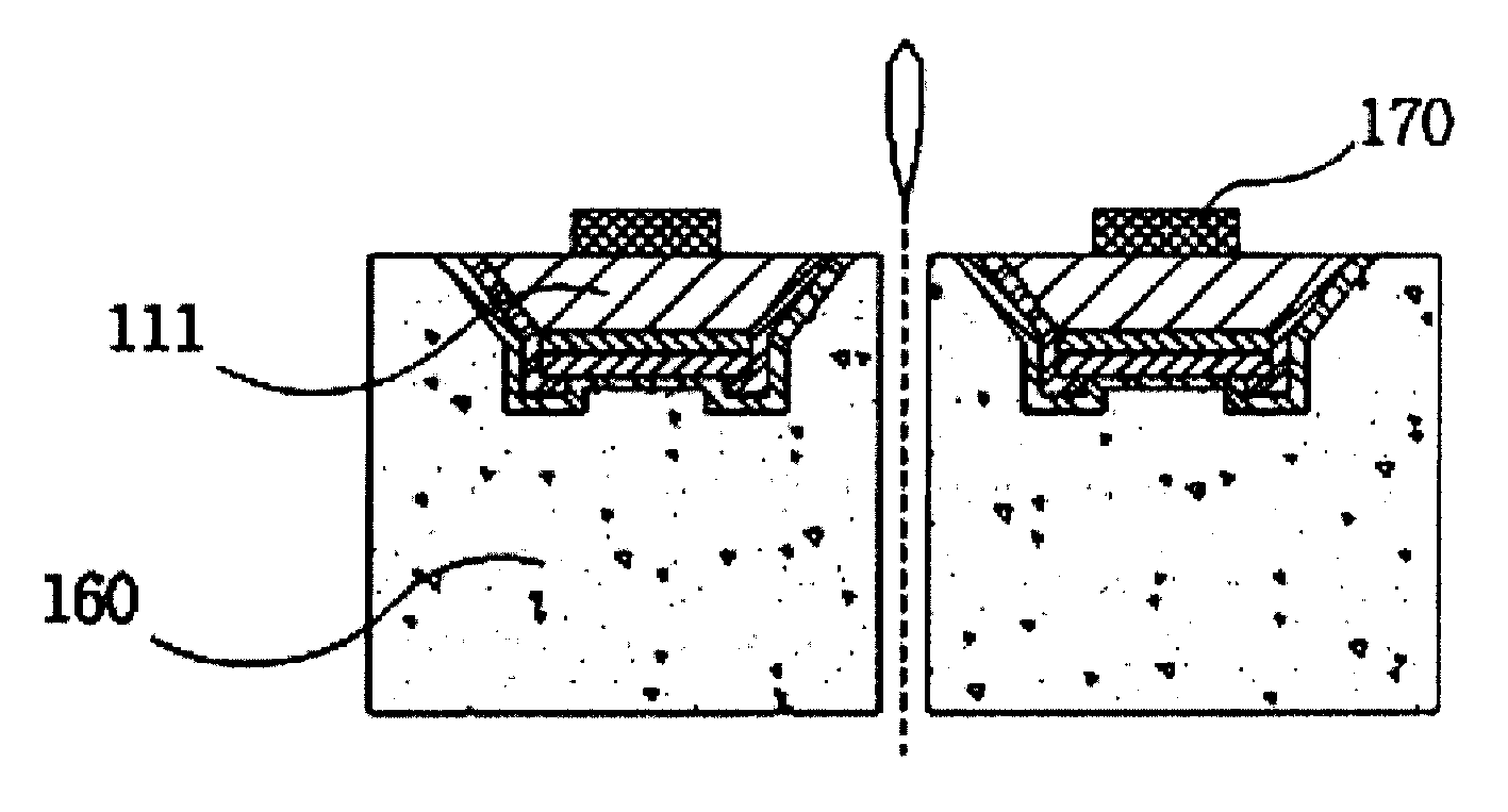
随后,在各器件111上形成N电极焊接层170(图4h)。Subsequently, an N-
最后,经过如划片处理和切断处理的切割过程将各器件111彼此分离开来(图4i)。Finally, the
如图5所示,通过进行上述方法按照本发明的第一实施例制造的发光器件包括:具有倾斜的侧壁并包括N半导体层、活性层和P半导体层的器件结构112;形成于上述器件结构112上的P电极焊接层120;形成于P电极焊接层120上的反射金属膜130;裹绕器件结构112、P电极焊接层120、反射金属膜130和反射金属膜顶部的一部分的钝化膜140;裹绕钝化层140的晶种金属层150;裹绕晶种金属层150和反射金属膜130的金属层160;和形成于上述器件结构112的底部上的N电极焊接层170。As shown in FIG. 5, the light-emitting device manufactured according to the first embodiment of the present invention by carrying out the above-mentioned method includes: a
优选半导体层为为氮化镓(GaN)层。Preferably, the semiconductor layer is a gallium nitride (GaN) layer.
此外,优选钝化层140具有距所述器件结构、P电极焊接层和反射金属膜的侧面的预定厚度。In addition, it is preferable that the
图6a至6f为按照本发明第二实施例发光器件制造方法的截面示意图。在蓝宝石衬底100的上表面上形成包括多个器件的薄膜层110,各器件具有N-GaN层、活性层和P-GaN层构成(图6a)。6a to 6f are schematic cross-sectional views of a method for manufacturing a light emitting device according to a second embodiment of the present invention. A
之后,薄膜层110上相继沉积作为P电极焊接层的P金属层210、反射金属膜220和金属层230(图6b)。Afterwards, a
随后,经过LLO处理蓝宝石衬底100与薄膜层110分离(图6c)。Subsequently, the
其后,对薄膜层110进行选择性蚀刻,使得该多个器件彼此分离(图6d)。Thereafter, the
此时,在图6c和图6d所示的过程之间,优选进行清洁处理。At this time, between the processes shown in Fig. 6c and Fig. 6d, a cleaning process is preferably performed.
随后,在各该多个器件111上形成作为N电极焊接层的N金属层170,并形成裹绕该多个器件111的钝化层180(图6e)。Subsequently, an
这里,钝化层180形成在除N金属170之外的暴露区域上,且N金属层170透过钝化层180暴露。Here, the passivation layer 180 is formed on the exposed region except the
最后,通过划片处理和分断处理将各器件111彼此分离(图6f)。Finally, the
因此,通过进行上述方法的本发明的第二实施例制造的发光器件包括:金属层230;形成于金属层230上的反射金属膜220;,形成于上述反射金属膜220上的第一电极焊接层210;形成于第一电极焊接层上,具有N-GaN层、活性层和P-GaN层的器件形成薄膜111;形成器件形成薄膜顶部的一部分的第二电极焊接层170;和裹绕上述器件形成薄膜和第二电极焊接层侧面的钝化层180。Therefore, the light-emitting device manufactured by the second embodiment of the present invention that performs the above-mentioned method includes: a
如上所述,本发明的发光器件具有如下优点:As mentioned above, the light emitting device of the present invention has the following advantages:
1)金属填充在器件的分离过程所形成的沟槽区域中,从而器件可受到保护,并且具有较之传统方法更优良的散热性。1) The metal is filled in the trench region formed during the separation process of the device, so that the device can be protected and has better heat dissipation than the traditional method.
2)由于LLO(激光剥离)处理采用由生长过程生长的厚金属膜,而不是两种异质衬底的结合,故由于金属间的紧密结合显著降低了空隙的发生率,从而降低了裂纹的发生率。2) Since the LLO (laser lift-off) process uses a thick metal film grown by the growth process instead of the combination of two heterogeneous substrates, the incidence of voids is significantly reduced due to the tight bonding between the metals, thereby reducing the probability of cracks incidence.
3)在器件分离过程中器件的薄膜层的侧壁形成为倾斜,故很容易在该器件的薄膜层的侧壁上生长另外的材料,且由于该器件的薄膜层的倾斜的切割平面可显著降低光损失。3) in the device separation process, the sidewall of the thin film layer of the device is formed as inclined, so it is easy to grow additional materials on the sidewall of the thin film layer of the device, and because the inclined cutting plane of the thin film layer of the device can significantly Reduce light loss.
4)由于不需要额外的粘合过程,整个加工工艺可得到简化。4) Since no additional bonding process is required, the entire manufacturing process can be simplified.
5)由于不需要用其它材料来填充器件间的蚀刻区域,整个加工工艺可得到简化。5) Since there is no need to use other materials to fill the etched regions between the devices, the entire manufacturing process can be simplified.
如前文所述,本发明还有一个优点在于,用金属填充在器件分离过程形成的沟槽区中,从而可保护器件并可确保优良的散热。As mentioned above, another advantage of the present invention is that the trench region formed during the device separation process is filled with metal, thereby protecting the device and ensuring excellent heat dissipation.
此外,本发明另一个优点在于,反射膜形成于器件形成薄膜的倾斜侧壁上,故而可减少通过器件侧面的光损失,以提高光性能。In addition, another advantage of the present invention is that the reflective film is formed on the sloped sidewall of the device forming film, so that light loss through the side of the device can be reduced to improve optical performance.
虽然本发明是结合本发明的优选实施例进行描述和说明的,但本发明并不仅限于这些实施例。本领域中的技术人员完全可以理解,在不背离本发明技术范围和精神的情况下,可对本发明作出各种相应修改和变化,因此显而易见,这些修改和变化都应属于本发明所附权利要求确定的保护范围之内。Although the invention has been described and illustrated in connection with preferred embodiments of the invention, the invention is not limited to these embodiments. Those skilled in the art can fully understand that without departing from the technical scope and spirit of the present invention, various corresponding modifications and changes can be made to the present invention, so it is obvious that these modifications and changes should all belong to the appended claims of the present invention within the defined scope of protection.
Claims (15)
Applications Claiming Priority (2)
| Application Number | Priority Date | Filing Date | Title |
|---|---|---|---|
| KR1020040090456 | 2004-11-08 | ||
| KR1020040090456A KR100667508B1 (en) | 2004-11-08 | 2004-11-08 | Light emitting device and manufacturing method thereof |
Publications (1)
| Publication Number | Publication Date |
|---|---|
| CN1790757A true CN1790757A (en) | 2006-06-21 |
Family
ID=35871084
Family Applications (1)
| Application Number | Title | Priority Date | Filing Date |
|---|---|---|---|
| CNA2005101156357A Pending CN1790757A (en) | 2004-11-08 | 2005-11-08 | Light emitting device and method for fabricating the same |
Country Status (7)
| Country | Link |
|---|---|
| US (1) | US8053795B2 (en) |
| EP (1) | EP1662587B1 (en) |
| JP (1) | JP4565391B2 (en) |
| KR (1) | KR100667508B1 (en) |
| CN (1) | CN1790757A (en) |
| AT (1) | ATE453214T1 (en) |
| DE (1) | DE602005018433D1 (en) |
Cited By (10)
| Publication number | Priority date | Publication date | Assignee | Title |
|---|---|---|---|---|
| CN100505351C (en) * | 2007-12-24 | 2009-06-24 | 厦门市三安光电科技有限公司 | Manufacturing method for laser stripping GaN-based light emitting device by using synthesis separation method |
| CN100536184C (en) * | 2006-08-23 | 2009-09-02 | 三星电机株式会社 | Vertical gallium nitride-based light emitting diode and method of manufacturing the same |
| US7768025B2 (en) | 2006-06-23 | 2010-08-03 | Lg Electronics Inc. | Light emitting diode having vertical topology and method of making the same |
| US8253146B2 (en) | 2009-10-29 | 2012-08-28 | Advanced Optoelectronic Technology, Inc. | LED die having heat dissipation layers |
| CN103117334A (en) * | 2011-11-17 | 2013-05-22 | 山东浪潮华光光电子股份有限公司 | GaN-based light emitting diode (LED) chips in vertical structure and manufacturing method thereof |
| CN103956336A (en) * | 2006-09-20 | 2014-07-30 | 伊利诺伊大学评议会 | Release strategies for making transferable semiconductor structures, devices and device components |
| CN101097983B (en) * | 2006-06-28 | 2015-05-06 | 日本冲信息株式会社 | Semiconductor device, LED head and image forming apparatus |
| CN105283967A (en) * | 2013-06-06 | 2016-01-27 | 欧司朗光电半导体有限公司 | Light-emitting diode with passivation layer |
| CN106848006A (en) * | 2015-12-03 | 2017-06-13 | 映瑞光电科技(上海)有限公司 | Flip LED chips and preparation method thereof |
| CN108417545A (en) * | 2018-05-14 | 2018-08-17 | 深圳市欧科力科技有限公司 | A kind of power device and preparation method thereof |
Families Citing this family (30)
| Publication number | Priority date | Publication date | Assignee | Title |
|---|---|---|---|---|
| KR100600371B1 (en) * | 2005-05-17 | 2006-07-18 | 엘지전자 주식회사 | Manufacturing method of light emitting device |
| EP1798781B1 (en) * | 2005-12-15 | 2009-08-05 | LG Electronics Inc. | LED having vertical structure and method for fabricating the same |
| KR100851403B1 (en) | 2006-07-31 | 2008-08-08 | 삼성전자주식회사 | Light emitting device and method for manufacturing light emitting device |
| KR100867541B1 (en) * | 2006-11-14 | 2008-11-06 | 삼성전기주식회사 | Manufacturing method of vertical light emitting device |
| JP4910664B2 (en) * | 2006-11-30 | 2012-04-04 | 豊田合成株式会社 | Method for manufacturing group III-V semiconductor device |
| US7781241B2 (en) | 2006-11-30 | 2010-08-24 | Toyoda Gosei Co., Ltd. | Group III-V semiconductor device and method for producing the same |
| JP4290745B2 (en) | 2007-03-16 | 2009-07-08 | 豊田合成株式会社 | Method for manufacturing group III-V semiconductor device |
| KR100856230B1 (en) * | 2007-03-21 | 2008-09-03 | 삼성전기주식회사 | Light emitting device, manufacturing method and monolithic light emitting diode array |
| DE102007030129A1 (en) * | 2007-06-29 | 2009-01-02 | Osram Opto Semiconductors Gmbh | Method for producing a plurality of optoelectronic components and optoelectronic component |
| GB0721957D0 (en) | 2007-11-08 | 2007-12-19 | Photonstar Led Ltd | Ultra high thermal performance packaging for optoelectronics devices |
| SG153673A1 (en) | 2007-12-10 | 2009-07-29 | Tinggi Tech Private Ltd | Fabrication of semiconductor devices |
| JP2009231595A (en) | 2008-03-24 | 2009-10-08 | Oki Data Corp | Method of manufacturing semiconductor device |
| KR100902150B1 (en) * | 2008-09-23 | 2009-06-10 | (주)큐엠씨 | Apparatus and method for manufacturing light emitting device |
| KR101064081B1 (en) | 2008-12-29 | 2011-09-08 | 엘지이노텍 주식회사 | Semiconductor light emitting device and manufacturing method thereof |
| KR100934636B1 (en) * | 2009-02-27 | 2009-12-31 | 한빔 주식회사 | Method for manufacturing light emitting diode device and intermediate for manufacturing same |
| JP5349260B2 (en) | 2009-11-19 | 2013-11-20 | 株式会社東芝 | Semiconductor light emitting device and manufacturing method thereof |
| WO2011069242A1 (en) * | 2009-12-09 | 2011-06-16 | Cooledge Lighting Inc. | Semiconductor dice transfer-enabling apparatus and method for manufacturing transfer-enabling apparatus |
| US20110151588A1 (en) * | 2009-12-17 | 2011-06-23 | Cooledge Lighting, Inc. | Method and magnetic transfer stamp for transferring semiconductor dice using magnetic transfer printing techniques |
| US8334152B2 (en) | 2009-12-18 | 2012-12-18 | Cooledge Lighting, Inc. | Method of manufacturing transferable elements incorporating radiation enabled lift off for allowing transfer from host substrate |
| KR101028277B1 (en) * | 2010-05-25 | 2011-04-11 | 엘지이노텍 주식회사 | Light emitting device, light emitting device manufacturing method, light emitting device package and light unit |
| CN102544251B (en) * | 2010-12-27 | 2014-05-07 | 同方光电科技有限公司 | Manufacturing method of large-power vertical light-emitting diode |
| DE102011104515A1 (en) * | 2011-06-17 | 2012-12-20 | Osram Opto Semiconductors Gmbh | Method for producing a plurality of optoelectronic semiconductor chips |
| TW201318223A (en) * | 2011-10-27 | 2013-05-01 | Ritedia Corp | Light emitting diode having aluminum nitride, chip on board comprising the same, and method of fabricating the same |
| WO2013084155A1 (en) * | 2011-12-08 | 2013-06-13 | Koninklijke Philips Electronics N.V. | Forming thick metal layers on a semiconductor light emitting device |
| KR101945791B1 (en) | 2012-03-14 | 2019-02-11 | 삼성전자주식회사 | Fabrication method of semiconductor light emitting device |
| US9337078B2 (en) | 2013-09-11 | 2016-05-10 | Globalfoundries Inc. | Heat dissipation through device isolation |
| US20150279815A1 (en) * | 2014-03-28 | 2015-10-01 | Stats Chippac, Ltd. | Semiconductor Device and Method of Forming Substrate Having Conductive Columns |
| KR102756760B1 (en) | 2019-08-21 | 2025-01-20 | 엘지전자 주식회사 | Manufacturing method of display device using semiconductor light emitting device |
| CN111679454B (en) * | 2020-06-19 | 2023-07-07 | 联合微电子中心有限责任公司 | Method for manufacturing semiconductor device |
| CN112447863B (en) * | 2020-11-20 | 2022-06-14 | 横店集团东磁股份有限公司 | Solar cell and preparation method thereof |
Family Cites Families (15)
| Publication number | Priority date | Publication date | Assignee | Title |
|---|---|---|---|---|
| JP3365787B2 (en) * | 1992-06-18 | 2003-01-14 | シャープ株式会社 | LED chip mounting parts |
| WO1998031055A1 (en) * | 1997-01-09 | 1998-07-16 | Nichia Chemical Industries, Ltd. | Nitride semiconductor device |
| US20010042866A1 (en) * | 1999-02-05 | 2001-11-22 | Carrie Carter Coman | Inxalygazn optical emitters fabricated via substrate removal |
| DE10040448A1 (en) * | 2000-08-18 | 2002-03-07 | Osram Opto Semiconductors Gmbh | Semiconductor chip and method for its production |
| US6657237B2 (en) * | 2000-12-18 | 2003-12-02 | Samsung Electro-Mechanics Co., Ltd. | GaN based group III-V nitride semiconductor light-emitting diode and method for fabricating the same |
| US6555405B2 (en) * | 2001-03-22 | 2003-04-29 | Uni Light Technology, Inc. | Method for forming a semiconductor device having a metal substrate |
| US8294172B2 (en) * | 2002-04-09 | 2012-10-23 | Lg Electronics Inc. | Method of fabricating vertical devices using a metal support film |
| US20030189215A1 (en) * | 2002-04-09 | 2003-10-09 | Jong-Lam Lee | Method of fabricating vertical structure leds |
| KR101030068B1 (en) * | 2002-07-08 | 2011-04-19 | 니치아 카가쿠 고교 가부시키가이샤 | Nitride semiconductor device manufacturing method and nitride semiconductor device |
| US7511311B2 (en) * | 2002-08-01 | 2009-03-31 | Nichia Corporation | Semiconductor light-emitting device, method for manufacturing the same, and light-emitting apparatus including the same |
| TWI228323B (en) * | 2002-09-06 | 2005-02-21 | Sony Corp | Semiconductor light emitting device and its manufacturing method, integrated semiconductor light emitting device and manufacturing method thereof, image display device and its manufacturing method, illumination device and manufacturing method thereof |
| DE10245631B4 (en) * | 2002-09-30 | 2022-01-20 | OSRAM Opto Semiconductors Gesellschaft mit beschränkter Haftung | semiconductor device |
| JP4143732B2 (en) * | 2002-10-16 | 2008-09-03 | スタンレー電気株式会社 | In-vehicle wavelength converter |
| US7244628B2 (en) * | 2003-05-22 | 2007-07-17 | Matsushita Electric Industrial Co., Ltd. | Method for fabricating semiconductor devices |
| JP2005268642A (en) * | 2004-03-19 | 2005-09-29 | Uni Light Technology Inc | Method for forming light emitting diode having metallic base |
-
2004
- 2004-11-08 KR KR1020040090456A patent/KR100667508B1/en not_active Expired - Fee Related
-
2005
- 2005-10-26 AT AT05292266T patent/ATE453214T1/en not_active IP Right Cessation
- 2005-10-26 EP EP05292266A patent/EP1662587B1/en not_active Ceased
- 2005-10-26 DE DE602005018433T patent/DE602005018433D1/en not_active Expired - Lifetime
- 2005-10-31 JP JP2005316839A patent/JP4565391B2/en not_active Expired - Fee Related
- 2005-11-07 US US11/267,320 patent/US8053795B2/en not_active Expired - Lifetime
- 2005-11-08 CN CNA2005101156357A patent/CN1790757A/en active Pending
Cited By (19)
| Publication number | Priority date | Publication date | Assignee | Title |
|---|---|---|---|---|
| US8624288B2 (en) | 2006-06-23 | 2014-01-07 | Lg Electronics, Inc. | Light emitting diode having vertical topology and method of making the same |
| US7834374B2 (en) | 2006-06-23 | 2010-11-16 | Lg Electronics Inc. | Light emitting diode having vertical topology and method of making the same |
| US7768025B2 (en) | 2006-06-23 | 2010-08-03 | Lg Electronics Inc. | Light emitting diode having vertical topology and method of making the same |
| US9530936B2 (en) | 2006-06-23 | 2016-12-27 | Lg Electronics Inc. | Light emitting diode having vertical topology and method of making the same |
| US8039281B2 (en) | 2006-06-23 | 2011-10-18 | Lg Electronics Inc. | Light emitting diode having vertical topology and method of making the same |
| CN101485000B (en) * | 2006-06-23 | 2012-01-11 | Lg电子株式会社 | Light emitting diode with vertical topology and method of manufacturing the same |
| CN102361052B (en) * | 2006-06-23 | 2015-09-30 | Lg电子株式会社 | Light emitting diode with vertical topology and method of manufacturing the same |
| CN101097983B (en) * | 2006-06-28 | 2015-05-06 | 日本冲信息株式会社 | Semiconductor device, LED head and image forming apparatus |
| CN100536184C (en) * | 2006-08-23 | 2009-09-02 | 三星电机株式会社 | Vertical gallium nitride-based light emitting diode and method of manufacturing the same |
| CN103956336A (en) * | 2006-09-20 | 2014-07-30 | 伊利诺伊大学评议会 | Release strategies for making transferable semiconductor structures, devices and device components |
| CN103956336B (en) * | 2006-09-20 | 2019-08-16 | 伊利诺伊大学评议会 | Release Strategies for Fabrication of Transferable Semiconductor Structures, Devices, and Device Components |
| CN100505351C (en) * | 2007-12-24 | 2009-06-24 | 厦门市三安光电科技有限公司 | Manufacturing method for laser stripping GaN-based light emitting device by using synthesis separation method |
| US8253146B2 (en) | 2009-10-29 | 2012-08-28 | Advanced Optoelectronic Technology, Inc. | LED die having heat dissipation layers |
| CN103117334A (en) * | 2011-11-17 | 2013-05-22 | 山东浪潮华光光电子股份有限公司 | GaN-based light emitting diode (LED) chips in vertical structure and manufacturing method thereof |
| CN103117334B (en) * | 2011-11-17 | 2015-05-06 | 山东浪潮华光光电子股份有限公司 | GaN-based light emitting diode (LED) chips in vertical structure and manufacturing method thereof |
| CN105283967A (en) * | 2013-06-06 | 2016-01-27 | 欧司朗光电半导体有限公司 | Light-emitting diode with passivation layer |
| CN105283967B (en) * | 2013-06-06 | 2018-05-11 | 欧司朗光电半导体有限公司 | light emitting diode with passivation layer |
| CN106848006A (en) * | 2015-12-03 | 2017-06-13 | 映瑞光电科技(上海)有限公司 | Flip LED chips and preparation method thereof |
| CN108417545A (en) * | 2018-05-14 | 2018-08-17 | 深圳市欧科力科技有限公司 | A kind of power device and preparation method thereof |
Also Published As
| Publication number | Publication date |
|---|---|
| JP4565391B2 (en) | 2010-10-20 |
| KR100667508B1 (en) | 2007-01-10 |
| US8053795B2 (en) | 2011-11-08 |
| EP1662587A3 (en) | 2007-08-29 |
| ATE453214T1 (en) | 2010-01-15 |
| KR20060041383A (en) | 2006-05-12 |
| EP1662587A2 (en) | 2006-05-31 |
| US20060097274A1 (en) | 2006-05-11 |
| EP1662587B1 (en) | 2009-12-23 |
| DE602005018433D1 (en) | 2010-02-04 |
| JP2006135321A (en) | 2006-05-25 |
Similar Documents
| Publication | Publication Date | Title |
|---|---|---|
| CN1790757A (en) | Light emitting device and method for fabricating the same | |
| JP5676396B2 (en) | Substrate removal method for high light extraction LED | |
| CN102315352B (en) | Light emitting semiconductor device and manufacture method thereof | |
| JP6522547B2 (en) | Passivation of semiconductor light emitting devices | |
| CN1292494C (en) | Light emitting semiconductor element and manufacturing method thereof | |
| CN101606246B (en) | Light emitting device using gan led chip | |
| CN100347866C (en) | Light emitting diodes including barrier layers/sublayers and manufacturing methods therefor | |
| CN1220280C (en) | Nitride semiconductor light emission device and its manufacture | |
| CN100505351C (en) | Manufacturing method for laser stripping GaN-based light emitting device by using synthesis separation method | |
| TW200417054A (en) | Trench cut light emitting diodes and methods of fabricating same | |
| CN1652364A (en) | Nitride-based light-emitting device and manufacturing method thereof | |
| TW201131819A (en) | Semiconductor light emitting device and method of fabricating semiconductor light emitting device | |
| CN1667847A (en) | Nitride semiconductor light emitting device | |
| CN102067341A (en) | Light emitting device and manufacturing method for same | |
| KR100890467B1 (en) | METHOD FOR PRODUCING THIN GaN LIGHT EMITTING DIODE DEVICE | |
| CN1582503A (en) | Light emitting diodes including modifications for submount bonding and manufacturing methods therefor | |
| CN1870312A (en) | Method of manufacturing light emitting diodes | |
| CN1471733A (en) | Manufacturing method of GaN-based semiconductor element | |
| CN1552103A (en) | Light emitting diodes including light extraction modifications and methods of making the same | |
| CN1744337A (en) | Nitride-based compound semiconductor light emitting device | |
| CN1933196A (en) | Light emitting devices and method for fabricating the same | |
| JP5185344B2 (en) | Semiconductor light emitting device manufacturing method and semiconductor light emitting device | |
| JP2010171371A (en) | Method for producing group-iii nitride-based compound semiconductor element | |
| CN103959487B (en) | Semiconductor light emitting device and manufacturing method thereof | |
| JP2004228290A (en) | Semiconductor light emitting element and its fabricating process |
Legal Events
| Date | Code | Title | Description |
|---|---|---|---|
| C06 | Publication | ||
| PB01 | Publication | ||
| C10 | Entry into substantive examination | ||
| SE01 | Entry into force of request for substantive examination | ||
| C12 | Rejection of a patent application after its publication | ||
| RJ01 | Rejection of invention patent application after publication |
Application publication date: 20060621 |