CN1653852A - Electroluminescence control panel - Google Patents
Electroluminescence control panel Download PDFInfo
- Publication number
- CN1653852A CN1653852A CNA038104695A CN03810469A CN1653852A CN 1653852 A CN1653852 A CN 1653852A CN A038104695 A CNA038104695 A CN A038104695A CN 03810469 A CN03810469 A CN 03810469A CN 1653852 A CN1653852 A CN 1653852A
- Authority
- CN
- China
- Prior art keywords
- layer
- hydrogen
- organic
- control board
- inhaling
- Prior art date
- Legal status (The legal status is an assumption and is not a legal conclusion. Google has not performed a legal analysis and makes no representation as to the accuracy of the status listed.)
- Pending
Links
- 238000005401 electroluminescence Methods 0.000 title claims description 5
- UFHFLCQGNIYNRP-UHFFFAOYSA-N Hydrogen Chemical compound [H][H] UFHFLCQGNIYNRP-UHFFFAOYSA-N 0.000 claims abstract description 57
- 239000001257 hydrogen Substances 0.000 claims abstract description 46
- 229910052739 hydrogen Inorganic materials 0.000 claims abstract description 46
- 229910010272 inorganic material Inorganic materials 0.000 claims abstract description 7
- 239000011147 inorganic material Substances 0.000 claims abstract description 7
- 239000010410 layer Substances 0.000 claims description 90
- 239000000463 material Substances 0.000 claims description 28
- 229910052751 metal Inorganic materials 0.000 claims description 7
- 239000002184 metal Substances 0.000 claims description 7
- 150000004767 nitrides Chemical class 0.000 claims description 6
- 239000000843 powder Substances 0.000 claims description 6
- 229910052783 alkali metal Inorganic materials 0.000 claims description 5
- 150000001340 alkali metals Chemical class 0.000 claims description 5
- 229910052784 alkaline earth metal Inorganic materials 0.000 claims description 5
- 150000001342 alkaline earth metals Chemical class 0.000 claims description 5
- 239000002808 molecular sieve Substances 0.000 claims description 4
- URGAHOPLAPQHLN-UHFFFAOYSA-N sodium aluminosilicate Chemical compound [Na+].[Al+3].[O-][Si]([O-])=O.[O-][Si]([O-])=O URGAHOPLAPQHLN-UHFFFAOYSA-N 0.000 claims description 4
- 229910052799 carbon Inorganic materials 0.000 claims description 3
- 229910052732 germanium Inorganic materials 0.000 claims description 3
- 229910052809 inorganic oxide Inorganic materials 0.000 claims description 3
- 239000011229 interlayer Substances 0.000 claims description 3
- 229910000765 intermetallic Inorganic materials 0.000 claims description 3
- 229910052747 lanthanoid Inorganic materials 0.000 claims description 3
- 150000002602 lanthanoids Chemical class 0.000 claims description 3
- 229910044991 metal oxide Inorganic materials 0.000 claims description 3
- 150000004706 metal oxides Chemical class 0.000 claims description 3
- 229910052759 nickel Inorganic materials 0.000 claims description 3
- 229910052703 rhodium Inorganic materials 0.000 claims description 3
- 229910052710 silicon Inorganic materials 0.000 claims description 3
- 229910052726 zirconium Inorganic materials 0.000 claims description 3
- 239000000203 mixture Substances 0.000 claims description 2
- 239000003795 chemical substances by application Substances 0.000 claims 8
- 239000000565 sealant Substances 0.000 claims 3
- 239000011159 matrix material Substances 0.000 claims 1
- 239000002245 particle Substances 0.000 claims 1
- 239000000758 substrate Substances 0.000 abstract description 17
- 238000007789 sealing Methods 0.000 abstract description 14
- 238000005538 encapsulation Methods 0.000 abstract description 6
- 239000007789 gas Substances 0.000 description 12
- KDLHZDBZIXYQEI-UHFFFAOYSA-N Palladium Chemical compound [Pd] KDLHZDBZIXYQEI-UHFFFAOYSA-N 0.000 description 9
- 239000011521 glass Substances 0.000 description 8
- 229920000642 polymer Polymers 0.000 description 7
- 239000012044 organic layer Substances 0.000 description 6
- 229920000620 organic polymer Polymers 0.000 description 5
- 229910052763 palladium Inorganic materials 0.000 description 5
- 229910045601 alloy Inorganic materials 0.000 description 4
- 239000000956 alloy Substances 0.000 description 4
- 229910018072 Al 2 O 3 Inorganic materials 0.000 description 3
- 239000000853 adhesive Substances 0.000 description 3
- 230000001070 adhesive effect Effects 0.000 description 3
- 238000006243 chemical reaction Methods 0.000 description 3
- 239000004020 conductor Substances 0.000 description 3
- 230000032798 delamination Effects 0.000 description 3
- 150000002431 hydrogen Chemical class 0.000 description 3
- 238000000034 method Methods 0.000 description 3
- -1 polyparaphenylene Polymers 0.000 description 3
- 239000011148 porous material Substances 0.000 description 3
- IJGRMHOSHXDMSA-UHFFFAOYSA-N Atomic nitrogen Chemical compound N#N IJGRMHOSHXDMSA-UHFFFAOYSA-N 0.000 description 2
- 229910052581 Si3N4 Inorganic materials 0.000 description 2
- 230000002745 absorbent Effects 0.000 description 2
- 239000002250 absorbent Substances 0.000 description 2
- 239000003513 alkali Substances 0.000 description 2
- QVGXLLKOCUKJST-UHFFFAOYSA-N atomic oxygen Chemical compound [O] QVGXLLKOCUKJST-UHFFFAOYSA-N 0.000 description 2
- 230000015572 biosynthetic process Effects 0.000 description 2
- 230000009172 bursting Effects 0.000 description 2
- 238000004132 cross linking Methods 0.000 description 2
- 239000012777 electrically insulating material Substances 0.000 description 2
- 238000005868 electrolysis reaction Methods 0.000 description 2
- 239000003822 epoxy resin Substances 0.000 description 2
- 238000001704 evaporation Methods 0.000 description 2
- 230000002687 intercalation Effects 0.000 description 2
- 238000009830 intercalation Methods 0.000 description 2
- 229910052745 lead Inorganic materials 0.000 description 2
- 239000011368 organic material Substances 0.000 description 2
- 239000001301 oxygen Substances 0.000 description 2
- 229910052760 oxygen Inorganic materials 0.000 description 2
- 229920000647 polyepoxide Polymers 0.000 description 2
- 229910052706 scandium Inorganic materials 0.000 description 2
- HQVNEWCFYHHQES-UHFFFAOYSA-N silicon nitride Chemical compound N12[Si]34N5[Si]62N3[Si]51N64 HQVNEWCFYHHQES-UHFFFAOYSA-N 0.000 description 2
- 238000005507 spraying Methods 0.000 description 2
- 238000003892 spreading Methods 0.000 description 2
- 239000000126 substance Substances 0.000 description 2
- 229910052718 tin Inorganic materials 0.000 description 2
- XLYOFNOQVPJJNP-UHFFFAOYSA-N water Substances O XLYOFNOQVPJJNP-UHFFFAOYSA-N 0.000 description 2
- 229910052727 yttrium Inorganic materials 0.000 description 2
- GOLORTLGFDVFDW-UHFFFAOYSA-N 3-(1h-benzimidazol-2-yl)-7-(diethylamino)chromen-2-one Chemical compound C1=CC=C2NC(C3=CC4=CC=C(C=C4OC3=O)N(CC)CC)=NC2=C1 GOLORTLGFDVFDW-UHFFFAOYSA-N 0.000 description 1
- 229920000265 Polyparaphenylene Polymers 0.000 description 1
- VYPSYNLAJGMNEJ-UHFFFAOYSA-N Silicium dioxide Chemical compound O=[Si]=O VYPSYNLAJGMNEJ-UHFFFAOYSA-N 0.000 description 1
- 229910052782 aluminium Inorganic materials 0.000 description 1
- XAGFODPZIPBFFR-UHFFFAOYSA-N aluminium Chemical compound [Al] XAGFODPZIPBFFR-UHFFFAOYSA-N 0.000 description 1
- PNEYBMLMFCGWSK-UHFFFAOYSA-N aluminium oxide Inorganic materials [O-2].[O-2].[O-2].[Al+3].[Al+3] PNEYBMLMFCGWSK-UHFFFAOYSA-N 0.000 description 1
- OKSRBEMKUSZPOX-UHFFFAOYSA-N aluminum;sodium;silicate Chemical group [Na+].[Al+3].[O-][Si]([O-])([O-])[O-] OKSRBEMKUSZPOX-UHFFFAOYSA-N 0.000 description 1
- 239000002585 base Substances 0.000 description 1
- 229910010293 ceramic material Inorganic materials 0.000 description 1
- 238000005229 chemical vapour deposition Methods 0.000 description 1
- 150000001875 compounds Chemical class 0.000 description 1
- 229920000547 conjugated polymer Polymers 0.000 description 1
- 229910052593 corundum Inorganic materials 0.000 description 1
- 238000005336 cracking Methods 0.000 description 1
- 230000001186 cumulative effect Effects 0.000 description 1
- 238000000151 deposition Methods 0.000 description 1
- 238000010586 diagram Methods 0.000 description 1
- 230000000694 effects Effects 0.000 description 1
- 229920006335 epoxy glue Polymers 0.000 description 1
- 230000008020 evaporation Effects 0.000 description 1
- 230000009477 glass transition Effects 0.000 description 1
- 238000013007 heat curing Methods 0.000 description 1
- 239000001307 helium Substances 0.000 description 1
- 229910052734 helium Inorganic materials 0.000 description 1
- SWQJXJOGLNCZEY-UHFFFAOYSA-N helium atom Chemical compound [He] SWQJXJOGLNCZEY-UHFFFAOYSA-N 0.000 description 1
- 239000003230 hygroscopic agent Substances 0.000 description 1
- AMGQUBHHOARCQH-UHFFFAOYSA-N indium;oxotin Chemical compound [In].[Sn]=O AMGQUBHHOARCQH-UHFFFAOYSA-N 0.000 description 1
- 238000007641 inkjet printing Methods 0.000 description 1
- 238000002844 melting Methods 0.000 description 1
- 229910052757 nitrogen Inorganic materials 0.000 description 1
- TWNQGVIAIRXVLR-UHFFFAOYSA-N oxo(oxoalumanyloxy)alumane Chemical compound O=[Al]O[Al]=O TWNQGVIAIRXVLR-UHFFFAOYSA-N 0.000 description 1
- 238000004806 packaging method and process Methods 0.000 description 1
- 238000005240 physical vapour deposition Methods 0.000 description 1
- 239000004033 plastic Substances 0.000 description 1
- 230000001681 protective effect Effects 0.000 description 1
- 229910052814 silicon oxide Inorganic materials 0.000 description 1
- 238000001771 vacuum deposition Methods 0.000 description 1
- 229910001845 yogo sapphire Inorganic materials 0.000 description 1
Images

Classifications
-
- H—ELECTRICITY
- H05—ELECTRIC TECHNIQUES NOT OTHERWISE PROVIDED FOR
- H05B—ELECTRIC HEATING; ELECTRIC LIGHT SOURCES NOT OTHERWISE PROVIDED FOR; CIRCUIT ARRANGEMENTS FOR ELECTRIC LIGHT SOURCES, IN GENERAL
- H05B33/00—Electroluminescent light sources
- H05B33/02—Details
- H05B33/04—Sealing arrangements, e.g. against humidity
-
- H—ELECTRICITY
- H10—SEMICONDUCTOR DEVICES; ELECTRIC SOLID-STATE DEVICES NOT OTHERWISE PROVIDED FOR
- H10K—ORGANIC ELECTRIC SOLID-STATE DEVICES
- H10K59/00—Integrated devices, or assemblies of multiple devices, comprising at least one organic light-emitting element covered by group H10K50/00
- H10K59/80—Constructional details
- H10K59/87—Passivation; Containers; Encapsulations
- H10K59/873—Encapsulations
-
- H—ELECTRICITY
- H10—SEMICONDUCTOR DEVICES; ELECTRIC SOLID-STATE DEVICES NOT OTHERWISE PROVIDED FOR
- H10K—ORGANIC ELECTRIC SOLID-STATE DEVICES
- H10K50/00—Organic light-emitting devices
- H10K50/80—Constructional details
- H10K50/84—Passivation; Containers; Encapsulations
- H10K50/844—Encapsulations
-
- H—ELECTRICITY
- H10—SEMICONDUCTOR DEVICES; ELECTRIC SOLID-STATE DEVICES NOT OTHERWISE PROVIDED FOR
- H10K—ORGANIC ELECTRIC SOLID-STATE DEVICES
- H10K50/00—Organic light-emitting devices
- H10K50/80—Constructional details
- H10K50/84—Passivation; Containers; Encapsulations
- H10K50/846—Passivation; Containers; Encapsulations comprising getter material or desiccants
-
- H—ELECTRICITY
- H10—SEMICONDUCTOR DEVICES; ELECTRIC SOLID-STATE DEVICES NOT OTHERWISE PROVIDED FOR
- H10K—ORGANIC ELECTRIC SOLID-STATE DEVICES
- H10K59/00—Integrated devices, or assemblies of multiple devices, comprising at least one organic light-emitting element covered by group H10K50/00
- H10K59/80—Constructional details
- H10K59/87—Passivation; Containers; Encapsulations
- H10K59/874—Passivation; Containers; Encapsulations including getter material or desiccant
-
- Y—GENERAL TAGGING OF NEW TECHNOLOGICAL DEVELOPMENTS; GENERAL TAGGING OF CROSS-SECTIONAL TECHNOLOGIES SPANNING OVER SEVERAL SECTIONS OF THE IPC; TECHNICAL SUBJECTS COVERED BY FORMER USPC CROSS-REFERENCE ART COLLECTIONS [XRACs] AND DIGESTS
- Y10—TECHNICAL SUBJECTS COVERED BY FORMER USPC
- Y10T—TECHNICAL SUBJECTS COVERED BY FORMER US CLASSIFICATION
- Y10T428/00—Stock material or miscellaneous articles
- Y10T428/31504—Composite [nonstructural laminate]
Landscapes
- Physics & Mathematics (AREA)
- Optics & Photonics (AREA)
- Electroluminescent Light Sources (AREA)
Abstract
Description
本发明涉及一种电致发光控制板,它包含一种能防止氧和湿气穿过的有机发光器件。US 5124204(连同图1一起)描述了一种常规的有机电致发光器件,它由一个形成在玻璃底板(2)上的透明的下电极(4),电致发光层(3),上电极(5)按以上次序制成。为了防止电致发光(EL)元件受潮,其上盖有一块密封板(7),利用粘结剂(6)例如环氧树脂将这密封板粘附在玻璃底板(2)上。在密封板(7)的下面放置了吸湿性材料(9)。The present invention relates to an electroluminescent control panel comprising an organic light emitting device which prevents the passage of oxygen and moisture. US 5124204 (together with Fig. 1) has described a kind of conventional organic electroluminescence device, and it is formed on the glass bottom plate (2) by a transparent lower electrode (4), electroluminescent layer (3), upper electrode (5) Made in the above order. In order to protect the electroluminescent (EL) element from moisture, it is covered with a sealing plate (7), which is adhered to the glass base (2) by means of an adhesive (6) such as epoxy resin. Below the sealing plate (7) a hygroscopic material (9) is placed.
为了获得高度可靠的有机电致发光器件,应有大量的吸湿性材料存在,以便能够在有机电致发光器件的整个使用寿命期间吸收湿气。这是由于这器件不是密封的,而环氧树脂胶液对湿气还有其它气体例如氧,氢,氮和氦而言是可渗透的。大量的吸湿性材料可能造成器件的总厚度增加。鉴于这一原因,就有了对(叠层式)密封式器件的探索。这一类器件可采用在有机机器件和基质的上方放置一层无机层的方法加以密封。如果这层材料是金属,必须添加附加的电绝缘的,不可渗透的层以防短路。In order to obtain a highly reliable organic electroluminescent device, a large amount of hygroscopic material should be present in order to be able to absorb moisture over the lifetime of the organic electroluminescent device. This is due to the fact that the device is not hermetic and the epoxy glue is permeable to moisture and other gases such as oxygen, hydrogen, nitrogen and helium. Large amounts of hygroscopic material may cause an increase in the overall thickness of the device. For this reason, there is a search for (stacked) hermetic devices. Such devices can be hermetically sealed by placing an inorganic layer over the organic device and substrate. If the material of this layer is metal, an additional electrically insulating, impermeable layer must be added to prevent short circuits.
可是,这一方法带来的问题似乎是控制板在工作过程中会产生氢气。这气体主要是由留在电致发光聚合物中的水电解产生的。在聚合物中发生的一些交联反应也会导致在系统中形成氢气。由于气体产生的结果可能会发生容积膨胀和爆裂和/或层离。However, the problem with this method seems to be that the control board generates hydrogen gas during operation. This gas is mainly produced by the electrolysis of water remaining in the electroluminescent polymer. Some crosslinking reactions that occur in polymers also lead to the formation of hydrogen gas in the system. Volume expansion and bursting and/or delamination may occur as a result of gas generation.
本发明的目的尤其是要提供一种改善了的密封式有机电致发光控制板。In particular, the object of the invention is to provide an improved sealed organic electroluminescence control panel.
按照本发明,前文中所述类型的有机电致发光控制板的特征在于,这密封层包含无机材料以及吸氢剂被放置在封装系统内位于与有机发光层呈实体接触的位置处。所谓的呈实体接触指的是呈接触状态或间接接触状态。直接接触是指例如吸气剂被配置在发光层周围的这种情况。间接接触意指通过气体可渗透层将吸气剂与有机器件隔开。例如,假若上电极层具有能使气体通过的针孔,这气体可渗透层可以是上电极层。According to the invention, an organic electroluminescent control panel of the type described above is characterized in that the sealing layer comprises an inorganic material and that a hydrogen getter is placed within the encapsulation system in physical contact with the organic light-emitting layer. The so-called physical contact refers to a contact state or an indirect contact state. The direct contact means, for example, that the getter is arranged around the light-emitting layer. Indirect contact means that the getter is separated from the organic device by a gas permeable layer. For example, the gas permeable layer may be the upper electrode layer if the upper electrode layer has pinholes through which gas can pass.
依靠与在工作过程中会产生氢气的有机发光层的实体接触,这吸氢剂能粘合,吸收或捕获所产生的氢。用这种方法能有效地防止爆裂和/或层离。By virtue of physical contact with the organic light-emitting layer which generates hydrogen gas during operation, the hydrogen getter binds, absorbs or traps the generated hydrogen. Cracking and/or delamination can be effectively prevented in this way.
一种优选的实施方案的特征在于,一层氢气可渗透层被放置在上电极层上,吸氢剂被放置在氢气可渗透层上并通过氢气可渗透层和上电极层上的针孔与有机发光层呈实体接触状态。A preferred embodiment is characterized in that a hydrogen permeable layer is placed on the upper electrode layer, and the hydrogen getter is placed on the hydrogen permeable layer and passes through the hydrogen permeable layer and the pinholes on the upper electrode layer and The organic light-emitting layer is in a physical contact state.
因这种方式而引起所产生的氢气发生累积反应,可通过使氢气散布在较大的表面(上电极的表面)上的方法来防止。The cumulative reaction of hydrogen generated in this way can be prevented by spreading the hydrogen over a large surface (the surface of the upper electrode).
按照再一个实施方案,氢气可渗透层包含无机氧化物或氮化物和/或钯。According to yet another embodiment, the hydrogen permeable layer comprises inorganic oxides or nitrides and/or palladium.
EP 777 280公开了一种叠层结构,其中的有机器件叠层组件被盖上了一层其上涂刷了低自由能金属层的有机缓冲层,它起着热系数匹配层的作用和起着吸气材料的作用。可是,在这类结构中,有机缓冲层的这种特殊的配置,使得吸气材料与有机器件的有机聚合物层不是处于实体接触状态,所以不能起到捕获由有机聚合物层产生的氢气的作用。在上述结构中,吸气材料仅能吸收位于缓冲层外表上的湿气等等。EP 777 280 discloses a stack structure in which the organic device stack assembly is covered with an organic buffer layer coated with a low free energy metal layer, which acts as a thermal coefficient matching layer and acts as a function of the getter material. However, in this type of structure, the special configuration of the organic buffer layer makes the getter material not in physical contact with the organic polymer layer of the organic device, so it cannot capture the hydrogen generated by the organic polymer layer. effect. In the above structure, the getter material can only absorb moisture or the like on the outer surface of the cushioning layer.
在本发明的范围内,适合用作氢气捕集器的材料是选自以下的材料或材料的组合物(合金或金属间化合物):Within the scope of the present invention, suitable materials for use as hydrogen traps are materials or combinations of materials (alloys or intermetallic compounds) selected from:
a)碱金属a) Alkali metal
b)碱土金属b) Alkaline earth metals
c)镧系c) Lanthanides
d)Sc,Yd) Sc, Y
e)Pd,Rh,Ni,Zre) Pd, Rh, Ni, Zr
非常有效的氢气捕集器由至少一种碱(碱土)金属与铝组成的合金形成(尤其是Ba4Al是一种良好的候选物),和由在C,Si,Ge,Sn或Pb中插入至少一种碱(碱土)金属的插层材料形成。尤其是Li插入C中的层间材料产生良好的结果。Very efficient hydrogen traps are formed from alloys of at least one alkali (alkaline earth) metal with aluminum (Ba 4 Al in particular is a good candidate), and by alloys in C, Si, Ge, Sn or Pb An intercalation material is formed that inserts at least one alkali (alkaline earth) metal. Especially interlayer materials with Li intercalation into C yield good results.
再者,可以使用一种分子筛粉末,例如可以使用以Al2O3为基础的、具有多个能用来捕获氢气的(小)孔的粉末。一个实例是钠-铝-硅酸盐(0.6K2O:4Na2O:Al2O3:2SiO2)。Furthermore, a molecular sieve powder can be used, for example based on Al2O3 , having a plurality of (small) pores which can be used to trap hydrogen gas. An example is sodium-aluminum-silicate (0.6K 2 O:4Na 2 O:Al 2 O 3 :2SiO 2 ).
上面e)项中的ZrPd化合物似乎是好的典型,尤其是Zr9Pd1。The ZrPd compounds in item e) above seem to be good examples, especially Zr 9 Pd 1 .
吸气材料层可以采用蒸发或喷涂的方法沉积而有利地形成。The layer of getter material can advantageously be deposited by evaporation or by spraying.
通过以下的描述连同优选实施方案及与其有关的附图一起,使得本发明的这些和其它的目的和特点变得更清楚了,其中附图:These and other objects and features of the present invention will become more apparent from the following description together with preferred embodiments and the accompanying drawings, wherein:
图1是现有技术的电致发光控制板的剖面示意图;Fig. 1 is the sectional schematic diagram of the electroluminescent control board of prior art;
图2是本发明的第一种实施方案的剖面示意图。Fig. 2 is a schematic cross-sectional view of a first embodiment of the present invention.
图3是本发明的另外的几种实施方案的剖面示意图。Fig. 3 is a schematic cross-sectional view of several other embodiments of the present invention.
图1表明一种电致发光(EL)显示器器件1,它包含玻璃基质2,借助于本领域熟知的方法,例如物理或化学气相沉积法或油墨喷印法,在其上沉积了若干层。这器件1包含了一层含有有机电致发光材料的活性层或发射层3,将其夹在由导电材料形成的二层图案型电极层的中间,这有机电致发光材料是例如香豆素(有机的LED),或共轭聚合物,如PPV(聚对亚苯1,2-亚乙烯基)或PPV-衍生物(聚合物LED)。在这实例中,电极层包含直接沉积在玻璃基质2上的第一电极4,和第二电极5,由此形成了发光二极管(LED)基体。至少电极4是由活性层3发射的光线可以透过的材料例如氧化铟锡(ITO)制成。在工作过程中,第一电极4被激励,以致它们相对于第二电极5是处于足够高的正电压下,从而注入活性层3上的孔。这发射层3可能包含一层或多个层的有机层。为了简便起见,在下文中,不管是一层还是多层有机层均采用一词“有机层”。Figure 1 shows an electroluminescent (EL)
由层3,4和5组成的叠层组件包含在由盖板7形成的空腔8内,通过粘结剂6,例如热固化双组分环氧树脂,将盖板固定在玻璃基质2上。由玻璃基质2与被粘结剂6密封在基质2上的盖板7形成的密封盒,在其里面是这样配置吸湿剂9的,要使这吸湿性材料与层3,4和5组成的叠层组件之间留有一定的间隔。例如,可以将吸湿剂9固定在盖板7上,如图1所示。The laminated assembly consisting of
图1现有技术结构的缺点在于不能制造得足够的薄以适应某些应用,如手机。A disadvantage of the prior art structure of Figure 1 is that it cannot be made thin enough for certain applications, such as cell phones.
本发明以极薄的电致发光控制板为目标,它是通过使有机器件和防护盖形成叠层组件来实现的。在这样的紧密结构中,其中的相邻各层处于实体接触状态,没有(可渗透的)粘结的接缝和没有吸湿剂(捕集器)。The present invention targets an extremely thin electroluminescent control panel by forming a laminated assembly of organic devices and protective covers. In such a compact structure, adjacent layers are in physical contact, with no (permeable) bonded seams and no moisture absorbents (traps).
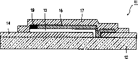
图2表明一种叠层组件(或叠层)式的电致发光控制板实例的横剖面图。基质12,可能是对湿气和气体来说是不可渗透的玻璃基质或者例如塑料基质,它承载着下电极层14,有机(聚合物)电致发光材料层13和上电极层15,它们在一起形成有机器件。覆盖住有机器件的无机材料密封层17使13,14和15组成的叠层组件整体化,这无机材料是例如碳化物或氮化物,尤其是氮化硅,或是电气绝缘的,湿气不可渗透的金属氧化物。密封层17连同基质12一起“封装”了有机器件。最后得到的EL控制板11可以非常的薄。Fig. 2 shows a cross-sectional view of an example of a laminated assembly (or laminated) type electroluminescence control panel. A
可是,这一方法带来的问题是控制板在工作过程中会产生氢气。这气体主要是由留在电致发光聚合物中的水电解产生的。在聚合物中发生的一些交联反应也会导致在系统中形成氢气。由于气体产生的结果可能会发生叠层组件容积膨胀和爆裂和/或层离。由于气密封装,故气体不可能逸出。However, the problem with this method is that the control board will generate hydrogen gas during operation. This gas is mainly produced by the electrolysis of water remaining in the electroluminescent polymer. Some crosslinking reactions that occur in polymers also lead to the formation of hydrogen gas in the system. Stack volume expansion and bursting and/or delamination may occur as a result of gas generation. Due to the hermetically sealed package, it is impossible for gas to escape.
为了解决这个问题,在13,14,15,17组成的叠层组件中安置了氢气捕集器19,使其位于与有机(聚合物)层13呈实体接触的位置处。在图2实施方案中,氢气捕集器19被安置成与有机(聚合物)层13的周边呈实体接触状态。假设层13有四条边,可以将氢气捕集器19安置成与层13的一条边或多条边的周边呈实体接触状态,To solve this problem, a
用作氢气捕集器19的适用的材料是Suitable materials for the
a)碱金属a) Alkali metal
b)碱土金属b) Alkaline earth metals
c)镧系c) Lanthanides
d)Sc,Yd) Sc, Y
e)Pd,Rh,Ni,Zre) Pd, Rh, Ni, Zr
和它们的组合物(合金和金属间化合物)and their compositions (alloys and intermetallic compounds)
更为适用的材料是由上述类,尤其是a)和b)类与Al组合形成的材料(尤其是Ba4Al)和由插入C,Si,Ge,Sn,Pb中的上述类材料,尤其是a)和b)类材料(尤其是插入C中的Li)形成的层间材料。More suitable materials are materials formed by the above-mentioned types, especially a) and b) in combination with Al (especially Ba 4 Al) and materials of the above-mentioned types inserted into C, Si, Ge, Sn, Pb, especially It is an interlayer material formed by materials of type a) and b) (especially Li intercalated in C).
也可使用各种分子筛粉末,例如可以使用以Al2O3为基础的、具有多个能用来捕获氢气的(小)孔的粉末。这种分子筛粉末是例如(0.6K2O:4Na2O:Al2O3:2SiO2)。Various molecular sieve powders can also be used, eg Al 2 O 3 -based powders with a number of (small) pores that can be used to trap hydrogen gas. Such a molecular sieve powder is, for example, (0.6K 2 O:4Na 2 O:Al 2 O 3 :2SiO 2 ).
图3表示图2结构的另一个替代方案,该图中与图2中的相同元件采用同样的编号。在上电极15的上表面上放置了氢气捕集器19。有机层13中产生的氢气可通过电极15上的针孔到达氢气捕集器19′。在本实施方案中,氢气捕集器19′与有机层13不是呈直接实体接触状态,而是呈实体接触状态(通过电极15上的针孔)。这一方案的缺点在于,如果在有机层13的一个区域产生(大量的)氢气,则氢气就会堆积在氢气捕集器19′上的一个区域内。这是不希望的。图4提出了一个解决这一问题的实施方案。Figure 3 shows another alternative to the structure of Figure 2, in which elements identical to those in Figure 2 are numbered the same. On the upper surface of the
图4表示图2结构的另一个替代方案,该图中与图2中的相同元件采用同样的编号。在既与聚合物层13又与吸氢剂19″呈实体接触的位置处,安置了氢气可渗透层18。按照这一方式,吸氢剂19″与聚合物层13呈实体接触。通过借助于氢气可渗透层18使氢气散布在较大的表面上的方法,防止了所产生的氢气堆积在一个区域内。FIG. 4 shows another alternative to the structure of FIG. 2, in which elements identical to those in FIG. 2 are numbered the same. At positions in physical contact with both the
层18可以是任何能使氢气渗透的材料。层18的一个非常特殊的实例是一种可使氢气穿过,但别的气体不能穿过的钯层。这类层的其它实例(它也可以是与钯的组合)是无机的氧化物,氮化物等等(例如氧化硅,氧化铝,氮化硅)。通常这些气体可渗透的材料的层可采用喷涂或蒸发方法制得。层18也可以是具有高玻璃化转变温度的有机物质。同样地,层30也可在电绝缘的有机或无机材料之中选取。Layer 18 may be any material that is permeable to hydrogen gas. A very specific example of layer 18 is a layer of palladium permeable to hydrogen but not to other gases. Other examples of such layers (which can also be in combination with palladium) are inorganic oxides, nitrides etc. (eg silicon oxide, aluminum oxide, silicon nitride). Typically layers of these gas permeable materials can be produced by spraying or evaporation methods. Layer 18 may also be an organic substance with a high glass transition temperature. Likewise, layer 30 may also be chosen among electrically insulating organic or inorganic materials.
为了能够产生一层无缺陷的无机密封层17,首先在由13,14,15组成的有机器件叠层组件上方沉积一层平面化层是有利的。吸氢剂层19′、19″的有利之处是能起到这种平面化层的作用。In order to be able to produce a defect-free
氮化物,氧氮化物,金属氧化物或金属,可以用作无机密封层17的材料。已经发现,例如Al的无缺陷层可采用真空沉积法沉积至厚度为500~5000,以便产生气密密封。Nitride, oxynitride, metal oxide or metal can be used as the material of the
在图5上表明使用的是金属密封层21(图5上编号为17),图中与图3中的相同元件采用同样的编号。It is indicated on FIG. 5 that a metal sealing layer 21 (numbered 17 on FIG. 5 ) is used, and the same elements in FIG. 3 are numbered the same.
在这种情况下,在这(金属)密封层21与下电极层14之间放置一种电绝缘物质16,以便防止发生短路。同样地,在沉积无机密封层17之前,至少要在上电极15的外露面上,沉积一层电绝缘材料层30。所采用的电绝缘材料可以是无机材料,例如低熔点玻璃或陶瓷材料,或有机材料。类似地,如果吸气剂19(图2)、19′(图3)或19″(图4)是属于导电材料,同时密封层17又选用导电材料例如像Al,则必须放置如同图5上的层30和16一样的电绝缘层以防止短路。In this case, an electrically insulating substance 16 is placed between the (metallic) sealing layer 21 and the
概括起来,本发明涉及一种叠层式电致发光控制板,它包含:In summary, the present invention relates to a laminated electroluminescent control panel comprising:
一个支承的透明基质;a supporting transparent substrate;
一个形成在透明基质上的分辨多个像素的有机器件;这有机器件包括介于上下电极层之间的有机发光层;和An organic device for resolving a plurality of pixels formed on a transparent substrate; the organic device includes an organic light-emitting layer between upper and lower electrode layers; and
放置一层与基质一起形成一种对有机器件的气密防湿封装系统的密封层。这密封层包含无机材料,吸氢剂则被放置在封装系统内位于与有机器件呈实体接触状态的位置处。这吸氢剂防止了由于有机器件在工作过程中所形成的氢气在封装系统内建立压力。A layer is placed together with the substrate to form a hermetic seal for the organic device's hermetic and moisture-tight encapsulation system. The sealing layer contains inorganic materials, and the hydrogen getter is placed in the encapsulation system at a position in physical contact with the organic device. This hydrogen getter prevents the build-up of pressure in the packaging system due to the hydrogen gas formed during the operation of the organic device.
Claims (10)
Applications Claiming Priority (2)
| Application Number | Priority Date | Filing Date | Title |
|---|---|---|---|
| EP02076852.9 | 2002-05-10 | ||
| EP02076852 | 2002-05-10 |
Publications (1)
| Publication Number | Publication Date |
|---|---|
| CN1653852A true CN1653852A (en) | 2005-08-10 |
Family
ID=29414776
Family Applications (1)
| Application Number | Title | Priority Date | Filing Date |
|---|---|---|---|
| CNA038104695A Pending CN1653852A (en) | 2002-05-10 | 2003-04-17 | Electroluminescence control panel |
Country Status (7)
| Country | Link |
|---|---|
| US (1) | US20050175841A1 (en) |
| EP (1) | EP1506694A1 (en) |
| JP (1) | JP2005525686A (en) |
| KR (1) | KR20040106513A (en) |
| CN (1) | CN1653852A (en) |
| AU (1) | AU2003222618A1 (en) |
| WO (1) | WO2003096752A1 (en) |
Cited By (4)
| Publication number | Priority date | Publication date | Assignee | Title |
|---|---|---|---|---|
| CN101341608B (en) * | 2005-12-19 | 2011-05-18 | 皇家飞利浦电子股份有限公司 | Organic led device |
| CN101771133B (en) * | 2009-01-04 | 2013-01-23 | 京东方科技集团股份有限公司 | Organic electroluminescence panel and manufacturing method thereof |
| CN104659060A (en) * | 2013-11-25 | 2015-05-27 | 乐金显示有限公司 | Array Substrate And Method Of Fabricating The Same |
| WO2020001121A1 (en) * | 2018-06-29 | 2020-01-02 | 京东方科技集团股份有限公司 | Packaging structure, display panel, display device and manufacturing method therefor |
Families Citing this family (6)
| Publication number | Priority date | Publication date | Assignee | Title |
|---|---|---|---|---|
| CN100539246C (en) * | 2004-09-27 | 2009-09-09 | 皇家飞利浦电子股份有限公司 | Illuminator |
| WO2009004690A1 (en) * | 2007-06-29 | 2009-01-08 | Pioneer Corporation | Organic semiconductor device and process for producing the same |
| WO2009096250A1 (en) * | 2008-02-01 | 2009-08-06 | Tokyo Electron Limited | Organic light-emitting diode, method for manufacturing organic light-emitting diode, manufacturing device for manufacturing organic light-emitting diode, and plasma processing device |
| KR101604139B1 (en) * | 2009-11-30 | 2016-03-17 | 엘지디스플레이 주식회사 | Organic light emitting diodde desplay device and fabricating method thereof |
| CN102326448B (en) * | 2010-03-01 | 2015-03-25 | 松下电器产业株式会社 | Organic EL device and method for manufacturing same |
| DE102016101710B4 (en) * | 2016-02-01 | 2025-02-06 | Pictiva Displays International Limited | OLED and method for producing an OLED |
Family Cites Families (9)
| Publication number | Priority date | Publication date | Assignee | Title |
|---|---|---|---|---|
| JP2742057B2 (en) * | 1988-07-14 | 1998-04-22 | シャープ株式会社 | Thin film EL panel |
| JP2787033B2 (en) * | 1991-11-11 | 1998-08-13 | セイコープレシジョン株式会社 | EL element |
| JPH05242966A (en) * | 1992-02-26 | 1993-09-21 | Nec Kansai Ltd | Electroluminescence lamp and manufacture thereof |
| IT1277457B1 (en) * | 1995-08-07 | 1997-11-10 | Getters Spa | COMBINATION OF GETTER MATERIALS AND RELATED DEVICE |
| US6673400B1 (en) * | 1996-10-15 | 2004-01-06 | Texas Instruments Incorporated | Hydrogen gettering system |
| US6069443A (en) * | 1997-06-23 | 2000-05-30 | Fed Corporation | Passive matrix OLED display |
| EP0993047A1 (en) * | 1998-10-06 | 2000-04-12 | Koninklijke Philips Electronics N.V. | Semiconductor device with elements of integrated circuits of III-V group and means to prevent the pollution by hydrogen |
| JP3409762B2 (en) * | 1999-12-16 | 2003-05-26 | 日本電気株式会社 | Organic electroluminescence device |
| US6936131B2 (en) * | 2002-01-31 | 2005-08-30 | 3M Innovative Properties Company | Encapsulation of organic electronic devices using adsorbent loaded adhesives |
-
2003
- 2003-04-17 CN CNA038104695A patent/CN1653852A/en active Pending
- 2003-04-17 EP EP03717457A patent/EP1506694A1/en not_active Withdrawn
- 2003-04-17 US US10/513,747 patent/US20050175841A1/en not_active Abandoned
- 2003-04-17 JP JP2004504572A patent/JP2005525686A/en not_active Withdrawn
- 2003-04-17 AU AU2003222618A patent/AU2003222618A1/en not_active Abandoned
- 2003-04-17 KR KR10-2004-7018073A patent/KR20040106513A/en not_active Application Discontinuation
- 2003-04-17 WO PCT/IB2003/001543 patent/WO2003096752A1/en not_active Application Discontinuation
Cited By (6)
| Publication number | Priority date | Publication date | Assignee | Title |
|---|---|---|---|---|
| CN101341608B (en) * | 2005-12-19 | 2011-05-18 | 皇家飞利浦电子股份有限公司 | Organic led device |
| CN101771133B (en) * | 2009-01-04 | 2013-01-23 | 京东方科技集团股份有限公司 | Organic electroluminescence panel and manufacturing method thereof |
| CN104659060A (en) * | 2013-11-25 | 2015-05-27 | 乐金显示有限公司 | Array Substrate And Method Of Fabricating The Same |
| CN104659060B (en) * | 2013-11-25 | 2018-08-31 | 乐金显示有限公司 | Array substrate and the method for manufacturing the array substrate |
| WO2020001121A1 (en) * | 2018-06-29 | 2020-01-02 | 京东方科技集团股份有限公司 | Packaging structure, display panel, display device and manufacturing method therefor |
| US11502275B2 (en) | 2018-06-29 | 2022-11-15 | Fuzhou Boe Optoelectronics Technology Co., Ltd. | Display panel, display device and manufacturing method thereof |
Also Published As
| Publication number | Publication date |
|---|---|
| EP1506694A1 (en) | 2005-02-16 |
| JP2005525686A (en) | 2005-08-25 |
| AU2003222618A1 (en) | 2003-11-11 |
| WO2003096752A1 (en) | 2003-11-20 |
| US20050175841A1 (en) | 2005-08-11 |
| KR20040106513A (en) | 2004-12-17 |
Similar Documents
| Publication | Publication Date | Title |
|---|---|---|
| CN103875090B (en) | Packaging part for organic electronic device | |
| JP5144041B2 (en) | ORGANIC ELECTROLUMINESCENT LIGHT EMITTING DEVICE AND ORGANIC ELECTROLUMINESCENT LIGHTING DEVICE | |
| US6803127B2 (en) | Encapsulation of an organic electro-luminescence element for a display device and method thereof | |
| US6737176B1 (en) | Organic electroluminescent device and method for fabricating same | |
| CN100468812C (en) | Electroluminescence control panel | |
| CN1287636C (en) | Encapsulation of polymer-based solid state devices with inorganic materials | |
| US20040108811A1 (en) | OLED Devices with Improved Encapsulation | |
| CN101331628A (en) | Electrode laminate for electroactive device and manufacturing method thereof | |
| CN103636023A (en) | Encapsulation structure for an opto-electronic component, and method for encapsulating an optoelectronic component | |
| TWI243627B (en) | EL device | |
| CN1653852A (en) | Electroluminescence control panel | |
| KR20110131381A (en) | OLED apparatus applying insulation and heat dissipation structure and its manufacturing method | |
| CN100352078C (en) | Encapsulation structure and encapsulation method of organic electroluminescence display element | |
| US8044583B2 (en) | Organic electroluminescent device without cap and getter | |
| CN1568100A (en) | Hygroscopic protective structure for organic light-emitting displays | |
| CN1381825A (en) | Method and structure for protecting organic electroluminescence display | |
| JP2002008854A (en) | Organic light emitting device | |
| CN2613053Y (en) | Organic Light Emitting Diodes with Water Removal Films | |
| CN1571602A (en) | Organic light emitting display and manufacturing method thereof | |
| JP4516299B2 (en) | Organic EL display device and manufacturing method thereof | |
| CN1571596A (en) | Encapsulation structure of high-intensity organic electroluminescent components |
Legal Events
| Date | Code | Title | Description |
|---|---|---|---|
| C06 | Publication | ||
| PB01 | Publication | ||
| C10 | Entry into substantive examination | ||
| SE01 | Entry into force of request for substantive examination | ||
| C02 | Deemed withdrawal of patent application after publication (patent law 2001) | ||
| WD01 | Invention patent application deemed withdrawn after publication |