CN1645618A - Semiconductor memory device and making method thereof - Google Patents
Semiconductor memory device and making method thereof Download PDFInfo
- Publication number
- CN1645618A CN1645618A CNA2005100047808A CN200510004780A CN1645618A CN 1645618 A CN1645618 A CN 1645618A CN A2005100047808 A CNA2005100047808 A CN A2005100047808A CN 200510004780 A CN200510004780 A CN 200510004780A CN 1645618 A CN1645618 A CN 1645618A
- Authority
- CN
- China
- Prior art keywords
- gate
- word line
- mentioned
- potential
- insulating film
- Prior art date
- Legal status (The legal status is an assumption and is not a legal conclusion. Google has not performed a legal analysis and makes no representation as to the accuracy of the status listed.)
- Granted
Links
- 239000004065 semiconductor Substances 0.000 title claims abstract description 114
- 238000000034 method Methods 0.000 title claims description 20
- 230000008878 coupling Effects 0.000 claims abstract description 13
- 238000010168 coupling process Methods 0.000 claims abstract description 13
- 238000005859 coupling reaction Methods 0.000 claims abstract description 13
- 239000010410 layer Substances 0.000 claims description 160
- 239000000758 substrate Substances 0.000 claims description 111
- 238000004519 manufacturing process Methods 0.000 claims description 101
- 239000011229 interlayer Substances 0.000 claims description 43
- 239000000463 material Substances 0.000 claims description 42
- 238000002955 isolation Methods 0.000 claims description 32
- 230000015572 biosynthetic process Effects 0.000 claims description 23
- 238000000151 deposition Methods 0.000 claims description 13
- 239000007772 electrode material Substances 0.000 claims description 11
- 230000006870 function Effects 0.000 claims description 10
- 238000009751 slip forming Methods 0.000 claims description 10
- 239000011159 matrix material Substances 0.000 claims description 6
- 239000012535 impurity Substances 0.000 claims description 5
- 238000003860 storage Methods 0.000 abstract description 12
- 229910052710 silicon Inorganic materials 0.000 description 158
- 239000010703 silicon Substances 0.000 description 158
- XUIMIQQOPSSXEZ-UHFFFAOYSA-N Silicon Chemical compound [Si] XUIMIQQOPSSXEZ-UHFFFAOYSA-N 0.000 description 151
- 108091006146 Channels Proteins 0.000 description 73
- 238000010586 diagram Methods 0.000 description 71
- VYPSYNLAJGMNEJ-UHFFFAOYSA-N Silicium dioxide Chemical compound O=[Si]=O VYPSYNLAJGMNEJ-UHFFFAOYSA-N 0.000 description 43
- 229910052814 silicon oxide Inorganic materials 0.000 description 43
- 229910052581 Si3N4 Inorganic materials 0.000 description 39
- HQVNEWCFYHHQES-UHFFFAOYSA-N silicon nitride Chemical compound N12[Si]34N5[Si]62N3[Si]51N64 HQVNEWCFYHHQES-UHFFFAOYSA-N 0.000 description 39
- 238000009792 diffusion process Methods 0.000 description 25
- 238000006243 chemical reaction Methods 0.000 description 24
- 229910021420 polycrystalline silicon Inorganic materials 0.000 description 23
- 229920005591 polysilicon Polymers 0.000 description 23
- 239000003990 capacitor Substances 0.000 description 18
- 238000005530 etching Methods 0.000 description 16
- 238000005468 ion implantation Methods 0.000 description 9
- 238000005498 polishing Methods 0.000 description 9
- 238000004088 simulation Methods 0.000 description 9
- 238000009825 accumulation Methods 0.000 description 8
- 238000000926 separation method Methods 0.000 description 8
- 239000000969 carrier Substances 0.000 description 7
- 230000008021 deposition Effects 0.000 description 7
- 230000000694 effects Effects 0.000 description 7
- 150000003376 silicon Chemical class 0.000 description 7
- BASFCYQUMIYNBI-UHFFFAOYSA-N platinum Chemical compound [Pt] BASFCYQUMIYNBI-UHFFFAOYSA-N 0.000 description 6
- 239000000126 substance Substances 0.000 description 6
- 230000014759 maintenance of location Effects 0.000 description 5
- 230000008569 process Effects 0.000 description 4
- 101100323157 Arabidopsis thaliana LAP1 gene Proteins 0.000 description 3
- 230000007423 decrease Effects 0.000 description 3
- 150000002500 ions Chemical class 0.000 description 3
- 229910052751 metal Inorganic materials 0.000 description 3
- 239000002184 metal Substances 0.000 description 3
- 230000003071 parasitic effect Effects 0.000 description 3
- 229910052697 platinum Inorganic materials 0.000 description 3
- 230000001681 protective effect Effects 0.000 description 3
- 230000009467 reduction Effects 0.000 description 3
- 101000979629 Homo sapiens Nucleoside diphosphate kinase A Proteins 0.000 description 2
- 102100023252 Nucleoside diphosphate kinase A Human genes 0.000 description 2
- 108010075750 P-Type Calcium Channels Proteins 0.000 description 2
- QVGXLLKOCUKJST-UHFFFAOYSA-N atomic oxygen Chemical compound [O] QVGXLLKOCUKJST-UHFFFAOYSA-N 0.000 description 2
- 210000000746 body region Anatomy 0.000 description 2
- 230000008859 change Effects 0.000 description 2
- 238000009413 insulation Methods 0.000 description 2
- 229910044991 metal oxide Inorganic materials 0.000 description 2
- 150000004706 metal oxides Chemical class 0.000 description 2
- 239000001301 oxygen Substances 0.000 description 2
- 229910052760 oxygen Inorganic materials 0.000 description 2
- 241000725302 Adult diarrheal rotavirus Species 0.000 description 1
- 101100298008 Strongylocentrotus purpuratus PM27 gene Proteins 0.000 description 1
- XJCLWVXTCRQIDI-UHFFFAOYSA-N Sulfallate Chemical compound CCN(CC)C(=S)SCC(Cl)=C XJCLWVXTCRQIDI-UHFFFAOYSA-N 0.000 description 1
- ATJFFYVFTNAWJD-UHFFFAOYSA-N Tin Chemical compound [Sn] ATJFFYVFTNAWJD-UHFFFAOYSA-N 0.000 description 1
- 238000003491 array Methods 0.000 description 1
- 230000004888 barrier function Effects 0.000 description 1
- 230000015556 catabolic process Effects 0.000 description 1
- 235000019504 cigarettes Nutrition 0.000 description 1
- 230000000295 complement effect Effects 0.000 description 1
- 239000004020 conductor Substances 0.000 description 1
- 238000010276 construction Methods 0.000 description 1
- 239000013078 crystal Substances 0.000 description 1
- 238000005137 deposition process Methods 0.000 description 1
- 230000001066 destructive effect Effects 0.000 description 1
- 238000001514 detection method Methods 0.000 description 1
- 230000009977 dual effect Effects 0.000 description 1
- 238000002474 experimental method Methods 0.000 description 1
- 229910052735 hafnium Inorganic materials 0.000 description 1
- VBJZVLUMGGDVMO-UHFFFAOYSA-N hafnium atom Chemical compound [Hf] VBJZVLUMGGDVMO-UHFFFAOYSA-N 0.000 description 1
- GPRLSGONYQIRFK-UHFFFAOYSA-N hydron Chemical compound [H+] GPRLSGONYQIRFK-UHFFFAOYSA-N 0.000 description 1
- 239000012212 insulator Substances 0.000 description 1
- 230000010354 integration Effects 0.000 description 1
- 230000003446 memory effect Effects 0.000 description 1
- 239000007769 metal material Substances 0.000 description 1
- 150000002739 metals Chemical class 0.000 description 1
- 230000004048 modification Effects 0.000 description 1
- 238000012986 modification Methods 0.000 description 1
- 238000000059 patterning Methods 0.000 description 1
- 230000008054 signal transmission Effects 0.000 description 1
- 230000001360 synchronised effect Effects 0.000 description 1
- 230000009466 transformation Effects 0.000 description 1
Images


Classifications
-
- H—ELECTRICITY
- H10—SEMICONDUCTOR DEVICES; ELECTRIC SOLID-STATE DEVICES NOT OTHERWISE PROVIDED FOR
- H10D—INORGANIC ELECTRIC SEMICONDUCTOR DEVICES
- H10D84/00—Integrated devices formed in or on semiconductor substrates that comprise only semiconducting layers, e.g. on Si wafers or on GaAs-on-Si wafers
-
- H—ELECTRICITY
- H10—SEMICONDUCTOR DEVICES; ELECTRIC SOLID-STATE DEVICES NOT OTHERWISE PROVIDED FOR
- H10D—INORGANIC ELECTRIC SEMICONDUCTOR DEVICES
- H10D30/00—Field-effect transistors [FET]
- H10D30/60—Insulated-gate field-effect transistors [IGFET]
- H10D30/711—Insulated-gate field-effect transistors [IGFET] having floating bodies
-
- G—PHYSICS
- G11—INFORMATION STORAGE
- G11C—STATIC STORES
- G11C11/00—Digital stores characterised by the use of particular electric or magnetic storage elements; Storage elements therefor
- G11C11/21—Digital stores characterised by the use of particular electric or magnetic storage elements; Storage elements therefor using electric elements
- G11C11/34—Digital stores characterised by the use of particular electric or magnetic storage elements; Storage elements therefor using electric elements using semiconductor devices
- G11C11/40—Digital stores characterised by the use of particular electric or magnetic storage elements; Storage elements therefor using electric elements using semiconductor devices using transistors
- G11C11/401—Digital stores characterised by the use of particular electric or magnetic storage elements; Storage elements therefor using electric elements using semiconductor devices using transistors forming cells needing refreshing or charge regeneration, i.e. dynamic cells
- G11C11/403—Digital stores characterised by the use of particular electric or magnetic storage elements; Storage elements therefor using electric elements using semiconductor devices using transistors forming cells needing refreshing or charge regeneration, i.e. dynamic cells with charge regeneration common to a multiplicity of memory cells, i.e. external refresh
- G11C11/404—Digital stores characterised by the use of particular electric or magnetic storage elements; Storage elements therefor using electric elements using semiconductor devices using transistors forming cells needing refreshing or charge regeneration, i.e. dynamic cells with charge regeneration common to a multiplicity of memory cells, i.e. external refresh with one charge-transfer gate, e.g. MOS transistor, per cell
-
- G—PHYSICS
- G11—INFORMATION STORAGE
- G11C—STATIC STORES
- G11C11/00—Digital stores characterised by the use of particular electric or magnetic storage elements; Storage elements therefor
- G11C11/21—Digital stores characterised by the use of particular electric or magnetic storage elements; Storage elements therefor using electric elements
- G11C11/34—Digital stores characterised by the use of particular electric or magnetic storage elements; Storage elements therefor using electric elements using semiconductor devices
- G11C11/40—Digital stores characterised by the use of particular electric or magnetic storage elements; Storage elements therefor using electric elements using semiconductor devices using transistors
- G11C11/401—Digital stores characterised by the use of particular electric or magnetic storage elements; Storage elements therefor using electric elements using semiconductor devices using transistors forming cells needing refreshing or charge regeneration, i.e. dynamic cells
- G11C11/4063—Auxiliary circuits, e.g. for addressing, decoding, driving, writing, sensing or timing
- G11C11/407—Auxiliary circuits, e.g. for addressing, decoding, driving, writing, sensing or timing for memory cells of the field-effect type
- G11C11/408—Address circuits
- G11C11/4085—Word line control circuits, e.g. word line drivers, - boosters, - pull-up, - pull-down, - precharge
-
- G—PHYSICS
- G11—INFORMATION STORAGE
- G11C—STATIC STORES
- G11C11/00—Digital stores characterised by the use of particular electric or magnetic storage elements; Storage elements therefor
- G11C11/21—Digital stores characterised by the use of particular electric or magnetic storage elements; Storage elements therefor using electric elements
- G11C11/34—Digital stores characterised by the use of particular electric or magnetic storage elements; Storage elements therefor using electric elements using semiconductor devices
- G11C11/40—Digital stores characterised by the use of particular electric or magnetic storage elements; Storage elements therefor using electric elements using semiconductor devices using transistors
- G11C11/401—Digital stores characterised by the use of particular electric or magnetic storage elements; Storage elements therefor using electric elements using semiconductor devices using transistors forming cells needing refreshing or charge regeneration, i.e. dynamic cells
- G11C11/4063—Auxiliary circuits, e.g. for addressing, decoding, driving, writing, sensing or timing
- G11C11/407—Auxiliary circuits, e.g. for addressing, decoding, driving, writing, sensing or timing for memory cells of the field-effect type
- G11C11/408—Address circuits
- G11C11/4087—Address decoders, e.g. bit - or word line decoders; Multiple line decoders
-
- H—ELECTRICITY
- H01—ELECTRIC ELEMENTS
- H01L—SEMICONDUCTOR DEVICES NOT COVERED BY CLASS H10
- H01L23/00—Details of semiconductor or other solid state devices
- H01L23/544—Marks applied to semiconductor devices or parts, e.g. registration marks, alignment structures, wafer maps
-
- H—ELECTRICITY
- H10—SEMICONDUCTOR DEVICES; ELECTRIC SOLID-STATE DEVICES NOT OTHERWISE PROVIDED FOR
- H10B—ELECTRONIC MEMORY DEVICES
- H10B12/00—Dynamic random access memory [DRAM] devices
-
- H—ELECTRICITY
- H10—SEMICONDUCTOR DEVICES; ELECTRIC SOLID-STATE DEVICES NOT OTHERWISE PROVIDED FOR
- H10B—ELECTRONIC MEMORY DEVICES
- H10B12/00—Dynamic random access memory [DRAM] devices
- H10B12/20—DRAM devices comprising floating-body transistors, e.g. floating-body cells
-
- H—ELECTRICITY
- H10—SEMICONDUCTOR DEVICES; ELECTRIC SOLID-STATE DEVICES NOT OTHERWISE PROVIDED FOR
- H10D—INORGANIC ELECTRIC SEMICONDUCTOR DEVICES
- H10D86/00—Integrated devices formed in or on insulating or conducting substrates, e.g. formed in silicon-on-insulator [SOI] substrates or on stainless steel or glass substrates
- H10D86/201—Integrated devices formed in or on insulating or conducting substrates, e.g. formed in silicon-on-insulator [SOI] substrates or on stainless steel or glass substrates the substrates comprising an insulating layer on a semiconductor body, e.g. SOI
-
- G—PHYSICS
- G11—INFORMATION STORAGE
- G11C—STATIC STORES
- G11C2211/00—Indexing scheme relating to digital stores characterized by the use of particular electric or magnetic storage elements; Storage elements therefor
- G11C2211/401—Indexing scheme relating to cells needing refreshing or charge regeneration, i.e. dynamic cells
- G11C2211/4016—Memory devices with silicon-on-insulator cells
-
- H—ELECTRICITY
- H01—ELECTRIC ELEMENTS
- H01L—SEMICONDUCTOR DEVICES NOT COVERED BY CLASS H10
- H01L2223/00—Details relating to semiconductor or other solid state devices covered by the group H01L23/00
- H01L2223/544—Marks applied to semiconductor devices or parts
- H01L2223/54426—Marks applied to semiconductor devices or parts for alignment
-
- H—ELECTRICITY
- H01—ELECTRIC ELEMENTS
- H01L—SEMICONDUCTOR DEVICES NOT COVERED BY CLASS H10
- H01L2223/00—Details relating to semiconductor or other solid state devices covered by the group H01L23/00
- H01L2223/544—Marks applied to semiconductor devices or parts
- H01L2223/54453—Marks applied to semiconductor devices or parts for use prior to dicing
-
- H—ELECTRICITY
- H01—ELECTRIC ELEMENTS
- H01L—SEMICONDUCTOR DEVICES NOT COVERED BY CLASS H10
- H01L2924/00—Indexing scheme for arrangements or methods for connecting or disconnecting semiconductor or solid-state bodies as covered by H01L24/00
- H01L2924/0001—Technical content checked by a classifier
- H01L2924/0002—Not covered by any one of groups H01L24/00, H01L24/00 and H01L2224/00
-
- H—ELECTRICITY
- H10—SEMICONDUCTOR DEVICES; ELECTRIC SOLID-STATE DEVICES NOT OTHERWISE PROVIDED FOR
- H10B—ELECTRONIC MEMORY DEVICES
- H10B12/00—Dynamic random access memory [DRAM] devices
- H10B12/01—Manufacture or treatment
Landscapes
- Engineering & Computer Science (AREA)
- Microelectronics & Electronic Packaging (AREA)
- Computer Hardware Design (AREA)
- Physics & Mathematics (AREA)
- Condensed Matter Physics & Semiconductors (AREA)
- General Physics & Mathematics (AREA)
- Power Engineering (AREA)
- Semiconductor Memories (AREA)
- Thin Film Transistor (AREA)
- Dram (AREA)
- Non-Volatile Memory (AREA)
Abstract
一种半导体存储器件,具有用于构成多个存储单元的多个MIS晶体管,其特征在于:各MIS晶体管包括:半导体层,在上述半导体层上形成的源极区域,在上述半导体层上与上述源极区域分离形成的漏极区域,使得上述源极区域和上述漏极区域之间的上述半导体层成为浮动状态的沟道体,设置在上述源极区域和上述漏极区域之间、用于在上述沟道体内、于上述源极区域和上述漏极区域之间形成沟道的主栅极,和为了通过电容耦合控制上述沟道体的电位、与上述主栅极分别设置的辅助栅极,该辅助栅极与上述主栅极同步驱动,并且上述MIS晶体管具有将上述沟道体设定在第1电位的第1数据状态和将上述沟道体设定在第2电位的第2数据状态。
A semiconductor storage device having a plurality of MIS transistors for constituting a plurality of memory cells, characterized in that each MIS transistor includes: a semiconductor layer, a source region formed on the semiconductor layer, and a The drain region formed by separating the source region so that the semiconductor layer between the source region and the drain region becomes a channel body in a floating state is arranged between the source region and the drain region for A main gate forming a channel between the source region and the drain region in the channel body, and an auxiliary gate provided separately from the main gate for controlling the potential of the channel body by capacitive coupling. , the auxiliary gate is synchronously driven with the main gate, and the MIS transistor has a first data state in which the channel body is set at a first potential and a second data state in which the channel body is set at a second potential state.
Description
本申请是申请日为2002年2月24日、申请号为02103395.1、发明名称为“半导体存储器件及其制造方法”的发明专利申请的分案申请。This application is a divisional application of the invention patent application with the filing date of February 24, 2002, the application number of 02103395.1, and the invention title of "semiconductor storage device and its manufacturing method".
技术领域technical field
本发明涉及用沟道体作为存储节点动态进行数据存储的半导体存储器件。The invention relates to a semiconductor storage device which uses a channel body as a storage node to dynamically store data.
背景技术Background technique
一般用作大容量RAM(随机存储器)的DRAM(动态随机存取存储器)的存储单元由一个MOS(金属氧化物半导体)晶体管和一个电容形成,用MOS晶体管作为选择开关将电荷存储在电容中。通过将存储在这个单元电容中的电荷作为位线电荷进行再分配,看到位线电位的变动,进行数据读出。所以,对于位线的初期电荷量在单元电容的存储电荷量中存在着下限。A memory cell of a DRAM (Dynamic Random Access Memory), which is generally used as a large-capacity RAM (Random Access Memory), is formed of a MOS (Metal Oxide Semiconductor) transistor and a capacitor, and charges are stored in the capacitor using the MOS transistor as a selection switch. By redistributing the charges stored in this cell capacitance as bit line charges, data is read out by seeing the change in bit line potential. Therefore, there is a lower limit on the amount of stored charge in the cell capacitor for the initial charge amount of the bit line.
在DRAM中,虽然伴随着微细化位线的寄生电容量下降,但是因为伴随着消耗电力的削减和微细化写入单元的电荷也下降,所以不会减少单元电容的电容量。电容的电容量与面积和电介质(电容绝缘膜)的介电常数成正比,与电容绝缘膜的膜厚成反比。因为当电容绝缘膜的膜厚变薄时由于隧道电流的流动而不能维持绝缘性,所以对于薄膜化存在着界限(约2nm),为了探索和开发通过增大硅氧化膜的介电常数抵消与二次方成比例的面积缩小,实现构造上稳定,符合硅CMOS(互补金属氧化物半导体)工艺,实际使用中可靠性高的电介质膜需要化费大量的时间和经费。In DRAM, although the parasitic capacitance of the bit line decreases with miniaturization, the electric charge written into the cell also decreases with the reduction of power consumption and miniaturization, so the capacitance of the cell capacitor does not decrease. The capacitance of the capacitor is proportional to the area and the dielectric constant of the dielectric (capacitor insulating film), and inversely proportional to the film thickness of the capacitor insulating film. Since the insulation cannot be maintained due to the flow of tunnel current when the film thickness of the capacitive insulating film is thinned, there is a limit (approximately 2nm) for thinning the film. The reduction in area proportional to the quadratic power achieves a stable structure, conforms to the silicon CMOS (complementary metal oxide semiconductor) process, and requires a lot of time and money for a highly reliable dielectric film in actual use.
为此,只在80年代后半期,才在DRAM的电容中使用堆叠单元构造和沟槽单元构造等3维构造。即便在这些堆叠单元构造和沟槽单元构造中,由于平面尺寸与3维深度之比最近才稍稍超过了10,呈纸卷香烟形状,在沟槽单元情形中对硅衬底的刻蚀界限,在堆叠单元的情形中与电容构造的下方物体和上方物体接触的接触孔的开口和进入其中的导体充填,电介质均匀覆盖性都成为问题,不能忍受100nm以下尺寸的进一步微细化。For this reason, three-dimensional structures such as stacked cell structure and trench cell structure were used in DRAM capacitors only in the second half of the 1980s. Even in these stacked cell configurations and trench cell configurations, since the ratio of planar size to 3D depth has only recently exceeded 10, in the shape of a paper cigarette, the etch limit to the silicon substrate in the trench cell case, In the case of stacked cells, the opening of the contact hole in contact with the lower and upper objects of the capacitor structure and the filling of the conductor entering it, and the uniform coverage of the dielectric become problems, and further miniaturization of the size below 100nm cannot be tolerated.
很早以来就进行了利用MOS的增益缩小电容的试验,并将这种类型的单元称为增益单元。因为通过读出MOS晶体管的栅极电位或者背栅电位,使漏电流发生变化,所以能够将增益单元大致分成将栅极作为存储节点,和将沟道体作为存储节点两大类。将读出MOS晶体管的栅极作为存储节点,过去就有Intel(英特尔)公司用于1k比特DRAM的3个晶体管和1个电容的构成与2个晶体管和1个电容的构成。至于电容可以利用主动形成的电容和寄生电容。无论用哪种电容,都存在着元件数在2以上,栅极(字线),漏极(位线)不共用,分成用于写入和用于读出两类,连线数也很多,不利于这些增益单元微细化等方面。Experiments have long been conducted using MOS gain reduction capacitors, and this type of unit is called a gain unit. Since the leakage current is changed by reading the gate potential or the back gate potential of the MOS transistor, gain cells can be broadly classified into two types, those using the gate as the storage node and those using the channel body as the storage node. The gate of the read MOS transistor is used as a storage node. In the past, Intel (Intel) has used three transistors and one capacitor for 1 kbit DRAM, and two transistors and one capacitor. As for the capacitance, actively formed capacitance and parasitic capacitance can be used. No matter what kind of capacitor is used, there are more than 2 components, and the gate (word line) and drain (bit line) are not shared. They are divided into two types for writing and reading, and there are many connections. This is not conducive to the miniaturization of these gain units.
也已经提出了用SOI(半导体氧化物绝缘体)衬底,将读出用MOS的沟道体作为存储节点存储电荷,利用背栅偏压效果的那种类型的增益单元的方案。例如,如下列文献所示。There has also been proposed a gain cell of the type that uses an SOI (Semiconductor Oxide Insulator) substrate, uses the channel body of a readout MOS as a storage node to store charge, and utilizes the back gate bias effect. For example, as shown in the following documents.
(1)H.Wann and C.Hu,“A capacitorless DRAM Cell on SOISustrate”,IEDM Digest of Technical Papers,pp.635-638,Dec.,1933,和(1) H.Wann and C.Hu, "A capacitorless DRAM Cell on SOISustrate", IEDM Digest of Technical Papers, pp.635-638, Dec., 1933, and
(2)M.R.Tack,et al,“The Multistable Charge Controlled MemoryEffect in SOI MOS Transistors at Low Temperatures”,IEEETransactions on Electron Devices,Vol.no.5,pp.1371-1382,May 1990。(2) M.R.Tack, et al, "The Multistable Charge Controlled Memory Effect in SOI MOS Transistors at Low Temperatures", IEEE Transactions on Electron Devices, Vol.no.5, pp.1371-1382, May 1990.
文献(1)乍一看可以看作是1个栅极的1个晶体管构成,但是实际上在栅极下面具有PMOS晶体管区域和NMOS晶体管区域,与简单的1个晶体管构造比较,尺寸变大。又,在写入“1”以前必须先写入“0”。即便从写入速度来说,与通常的SRAM,DRAM比较也是不利的。在由同一作者提出的特表平9-509284号公报中,也显示了在写入“1”以前不需要先写入“0”的工作例,但是在栅极下面具有PMOS晶体管区域和NMOS晶体管区域这一点没有改变。Document (1) can be regarded as a single transistor structure with one gate at first glance, but actually has a PMOS transistor region and an NMOS transistor region under the gate, and is larger in size than a simple single transistor structure. Also, "0" must be written before writing "1". Even in terms of writing speed, it is unfavorable compared with ordinary SRAM and DRAM. Japanese Patent Application Publication No. Hei 9-509284 proposed by the same author also shows an example of operation in which it is not necessary to write "0" before writing "1", but there is a PMOS transistor region and an NMOS transistor under the gate. This has not changed for the region.
文献(2),对于共用字线的单元,不能同时写入“1”和“0”,需要利用SOI衬底的消去工作。写入速度与通常的SRAM,DRAM比较也是不利的。Document (2), for cells that share a word line, "1" and "0" cannot be written at the same time, and it is necessary to use the erasing work of the SOI substrate. The writing speed is also unfavorable compared with common SRAM and DRAM.
在日本平成3年公开的3-171768号专利公报中,也显示了将沟道体作为存储节点存储电荷,利用背栅偏压效果的那种类型的增益单元。它需要将不与位线连接一侧的源极/漏极分离到位线方向或字线方向,从而尺寸变大。又,在写入“1”以前必须先写入“0”,从写入速度来说,与通常的SRAM,DRAM比较是不利的。Japanese Patent Publication No. 3-171768 published in 2013 also shows a gain unit of the type that uses the channel body as a storage node to store charges and utilizes the effect of the back gate bias. It needs to separate the source/drain on the side not connected to the bit line to the bit line direction or the word line direction, so that the size becomes large. Also, "0" must be written before writing "1", which is disadvantageous compared with ordinary SRAM and DRAM in terms of writing speed.
日本平成8年公开的8-213624号专利公报是将沟道体作为存储节点存储电荷,利用由沟道体的电位引起的寄生双极的收集极电流中的差的那种类型的增益单元。它也在写入“0”以前必须先写入“1”,从写入速度来说,与通常的SRAM,DRAM比较是不利的。Japanese Patent Publication No. 8-213624 published in 1999 is a gain unit of the type that uses the channel body as a storage node to store charges and utilizes the difference in the parasitic bipolar collector current caused by the potential of the channel body. It must also write "1" before writing "0". From the perspective of writing speed, it is unfavorable compared with ordinary SRAM and DRAM.
如上所述,最近提出的新的DRAM方案需要特殊的晶体管构造等,构造复杂,或者即便构造比较简单但是在控制性方面存在难点,难以达到高集成化和高性能的目的。As mentioned above, recently proposed new DRAM schemes require a special transistor structure, etc., and the structure is complicated, or even if the structure is relatively simple, there are difficulties in controllability, and it is difficult to achieve high integration and high performance.
发明内容Contents of the invention
本发明提供了一种半导体存储器件,具有用于构成多个存储单元的多个MIS晶体管,其特征在于:各MIS晶体管包括:半导体层,在上述半导体层上形成的源极区域,在上述半导体层上与上述源极区域分离形成的漏极区域,使得上述源极区域和上述漏极区域之间的上述半导体层成为浮动状态的沟道体,设置在上述源极区域和上述漏极区域之间、用于在上述沟道体内、于上述源极区域和上述漏极区域之间形成沟道的主栅极,和为了通过电容耦合控制上述沟道体的电位、与上述主栅极分别设置的辅助栅极,该辅助栅极与上述主栅极同步驱动,并且上述MIS晶体管具有将上述沟道体设定在第1电位的第1数据状态和将上述沟道体设定在第2电位的第2数据状态。The present invention provides a semiconductor memory device having a plurality of MIS transistors for constituting a plurality of memory cells, wherein each MIS transistor includes: a semiconductor layer, a source region formed on the semiconductor layer, The drain region formed separately from the above-mentioned source region on the layer, so that the above-mentioned semiconductor layer between the above-mentioned source region and the above-mentioned drain region becomes a channel body in a floating state, and is arranged between the above-mentioned source region and the above-mentioned drain region between the main gate for forming a channel in the channel body between the source region and the drain region, and for controlling the potential of the channel body through capacitive coupling, and separately from the main gate The auxiliary gate is driven synchronously with the main gate, and the MIS transistor has a first data state of setting the channel body at the first potential and setting the channel body at the second potential. The 2nd data state.
本发明还提供了一种半导体存储器件,具有用于构成多个存储单元的多个MIS晶体管,其中各MIS晶体管是具有第1数据状态和第2数据状态的半导体存储器件,该半导体存储器件包括:第1半导体衬底,在上述第1半导体衬底的表面上、以底面和侧面被绝缘膜覆盖的状态在一个方向上连续地形成的上述MIS晶体管的辅助栅极,隔着第1栅极绝缘膜设置在上述辅助栅极表面上的第2半导体衬底,在上述第2半导体衬底表面上、隔着第2栅极绝缘膜与上述辅助栅极并行连续地形成的上述MIS晶体管的主栅极,在上述第2半导体衬底上的、上述主栅极和上述辅助栅极的间隙部分上形成的源极区域,在上述第2半导体衬底上的、上述主栅极和上述辅助栅极的间隙部分上与上述源极区域分离地形成的漏极区域,与上述源极区域接触的,与上述主栅极和上述辅助栅极并行连续地设置的源极配线,覆盖上述源极配线的层间绝缘膜,和在上述层间绝缘膜上,在与上述主栅极和上述辅助栅极交叉的方向上形成的,与上述漏极区域接触的位线。The present invention also provides a semiconductor memory device having a plurality of MIS transistors for forming a plurality of memory cells, wherein each MIS transistor is a semiconductor memory device having a first data state and a second data state, and the semiconductor memory device includes : A first semiconductor substrate, on the surface of the above-mentioned first semiconductor substrate, the auxiliary gate of the above-mentioned MIS transistor formed continuously in one direction in a state where the bottom surface and the side surface are covered with an insulating film, with the first gate interposed therebetween A second semiconductor substrate with an insulating film provided on the surface of the auxiliary gate, and a main body of the MIS transistor formed on the surface of the second semiconductor substrate in parallel with the auxiliary gate via the second gate insulating film. The gate is a source region formed on the gap between the main gate and the auxiliary gate on the second semiconductor substrate, and the main gate and the auxiliary gate are formed on the second semiconductor substrate. The drain region formed separately from the above-mentioned source region on the gap part of the electrode, the source wiring that is in contact with the above-mentioned source region, provided in parallel with the above-mentioned main gate and the above-mentioned auxiliary gate, covers the above-mentioned source. An interlayer insulating film for wiring, and a bit line in contact with the drain region formed on the interlayer insulating film in a direction crossing the main gate and the auxiliary gate.
本发明提供了一种半导体存储器件的制造方法,其特征在于包括下列步骤:隔着第1绝缘膜在半导体衬底上形成半导体层,在上述半导体层中埋入用于在第1方向上划分使元件分离的元件形成区域的元件分离绝缘膜,在上述元件分离绝缘膜中,隔着第1栅极绝缘膜,埋入与上述半导体层侧面相对的主栅极,在上述半导体层上面,以与上述主栅极电连接的状态并且用功函数与上述主栅极不同的材料、隔着第2栅极绝缘膜形成与上述半导体层相对的辅助栅极,和将上述辅助栅极作为掩模,在上述半导体层中离子注入杂质形成源极区域和漏极区域。The present invention provides a method for manufacturing a semiconductor memory device, which is characterized by comprising the following steps: forming a semiconductor layer on a semiconductor substrate through a first insulating film, and embedding a semiconductor layer for dividing in the first direction in the semiconductor layer. In the element isolation insulating film in the element formation region for separating the elements, the main gate opposite to the side surface of the above-mentioned semiconductor layer is embedded in the above-mentioned element isolation insulating film through the first gate insulating film, and on the above-mentioned semiconductor layer, the In a state of being electrically connected to the above-mentioned main gate and using a material having a work function different from that of the above-mentioned main gate, forming an auxiliary gate opposite to the above-mentioned semiconductor layer through a second gate insulating film, and using the above-mentioned auxiliary gate as a mask, Impurities are ion-implanted into the above semiconductor layer to form a source region and a drain region.
本发明还提供了一种半导体存储器件的制造方法,其特征在于包括下列步骤:隔着第1绝缘膜在第1半导体衬底上形成栅极电极材料膜,隔着第1栅极绝缘膜、将第2半导体衬底粘合在上述栅极电极材料膜上,在上述第2半导体衬底上形成元件分离绝缘膜,带状地划分在第1方向连续的元件形成区域,在划分上述元件形成区域的第2半导体衬底上,淀积第2绝缘膜,将它作为在与上述第1方向交叉的第2方向上连续的伪栅极形成布局图案,将上述伪栅极作为掩模,依次刻蚀上述第2半导体衬底,上述第1栅极绝缘膜和上述栅极材料膜,在上述第2方向上连续地形成由上述栅极电极材料膜构成的辅助栅极,在上述伪栅极的间隙中埋入第3绝缘膜,直至第2半导体衬底的厚度方向的中间,在上述伪栅极的间隙中的上述第3绝缘膜上,形成侧面与上述第2半导体衬底连接的半导体层,除去上述伪栅极,在露出的上述第2半导体衬底的表面上形成第2栅极绝缘膜,在上述半导体层的间隙部分埋入与上述辅助栅极并行地连续的主栅极,通过在上述半导体层中离子注入杂质形成源极区域和漏极区域,形成与上述源极区域接触、在上述第2方向上连续的源极配线,和形成覆盖上述源极配线的层间绝缘膜,在该层间绝缘膜上形成与上述漏极区域接触的、在上述第1方向上连续的位线。The present invention also provides a method for manufacturing a semiconductor storage device, which is characterized by comprising the following steps: forming a gate electrode material film on a first semiconductor substrate via a first insulating film, and forming a gate electrode material film via a first gate insulating film, A second semiconductor substrate is adhered to the above-mentioned gate electrode material film, an element isolation insulating film is formed on the above-mentioned second semiconductor substrate, and the element formation region continuous in the first direction is divided into strips, and the element formation region is divided into strips. On the second semiconductor substrate in the region, deposit a second insulating film, use it as a dummy gate continuous in the second direction intersecting with the first direction to form a layout pattern, use the dummy gate as a mask, and sequentially Etching the above-mentioned second semiconductor substrate, the above-mentioned first gate insulating film and the above-mentioned gate material film, continuously forming the auxiliary gate composed of the above-mentioned gate electrode material film in the above-mentioned second direction, and forming the auxiliary gate formed by the above-mentioned dummy gate The third insulating film is buried in the gap between the dummy gates until the middle of the thickness direction of the second semiconductor substrate. On the third insulating film in the gap between the dummy gates, a semiconductor substrate connected to the second semiconductor substrate at the side is formed. layer, remove the dummy gate, form a second gate insulating film on the exposed surface of the second semiconductor substrate, and bury a main gate parallel to the auxiliary gate in the gap part of the semiconductor layer, Forming a source region and a drain region by ion-implanting impurities into the above-mentioned semiconductor layer, forming a source wiring continuous in the second direction in contact with the above-mentioned source region, and forming an interlayer covering the above-mentioned source wiring. An insulating film is formed on the interlayer insulating film to form a bit line in contact with the drain region and continuous in the first direction.
附图说明Description of drawings
图1是表示用于各实施形态的DRAM单元的基本构造的图。FIG. 1 is a diagram showing a basic structure of a DRAM cell used in each embodiment.
图2是表示用于说明同一DRAM单元的工作原理的体电位与栅极偏压之间关系的图。FIG. 2 is a diagram showing the relationship between body potential and gate bias voltage for explaining the operation principle of the same DRAM cell.
图3是表示根据本发明实施形态1的DRAM单元的截面构造的图。Fig. 3 is a diagram showing a cross-sectional structure of a DRAM cell according to
图4是用同一DRAM单元的单元阵列的等效电路图。Fig. 4 is an equivalent circuit diagram of a cell array using the same DRAM cell.
图5是同一单元阵列的布局图。Fig. 5 is a layout diagram of the same cell array.
图6A是图5的A-A′线截面图。Fig. 6A is a sectional view taken along line A-A' of Fig. 5 .
图6B是图5的B-B′线截面图。Fig. 6B is a sectional view taken along line B-B' of Fig. 5 .
图7A是表示用相同材料形成第1栅极和第2栅极时,同一DRAM单元的写入工作的波形图。7A is a waveform diagram showing a write operation of the same DRAM cell when the first gate and the second gate are formed of the same material.
图7B是表示用具有不同功函数的材料形成第1栅极和第2栅极时,同一DRAM单元的写入工作的波形图。7B is a waveform diagram showing a write operation of the same DRAM cell when the first gate and the second gate are formed of materials having different work functions.
图7C是表示为了产生图7B的写入工作波形的字线驱动器和行译码器的电路构成的一个例子的图。FIG. 7C is a diagram showing an example of a circuit configuration of a word line driver and a row decoder for generating the write operation waveform of FIG. 7B.
图7D是表示图7C所示的字线驱动器的变型例的图。FIG. 7D is a diagram showing a modified example of the word line driver shown in FIG. 7C.
图7E是表示当对于存储单元阵列配置图7C或图7D所示的行译码器和字线驱动器时的布局的一个例子的图(单侧配置)。7E is a diagram showing an example of a layout when the row decoder and the word line driver shown in FIG. 7C or 7D are arranged for a memory cell array (one-sided arrangement).
图7F是表示当对于存储单元阵列配置图7C或图7D所示的行译码器和字线驱动器时的布局的一个例子的图(两侧配置)。FIG. 7F is a diagram showing an example of a layout when the row decoders and word line drivers shown in FIG. 7C or 7D are arranged for a memory cell array (two-side arrangement).
图7G是表示为了产生图7A的写入工作波形的字线驱动器和行译码器的电路构成的一个例子的图。FIG. 7G is a diagram showing an example of a circuit configuration of a word line driver and a row decoder for generating the write operation waveform of FIG. 7A.
图7H是表示图7G所示的字线驱动器的变形例的图。FIG. 7H is a diagram showing a modified example of the word line driver shown in FIG. 7G.
图7I是表示当对于存储单元阵列配置图7G或图7H所示的行译码器和字线驱动器时的布局的一个例子的图(对于由第1字线和第2字线组成的字线对,左右互交地设置行译码器和字线驱动器的情形)。7I is a diagram showing an example of a layout when the row decoder and the word line driver shown in FIG. 7G or FIG. 7H are configured for the memory cell array (for a word line composed of a first word line and a second word line Yes, the case where the row decoder and the word line driver are alternately arranged left and right).
图7J是表示当对于存储单元阵列配置图7G或图7H所示的行译码器和字线驱动器时的布局的一个例子的图(在单侧设置用于第1字线的行译码器和字线驱动器,在另一单侧设置用于第2字线的行译码器和字线驱动器的情形)。7J is a diagram showing an example of a layout when the row decoder and the word line driver shown in FIG. 7G or FIG. 7H are arranged for the memory cell array (the row decoder for the first word line is provided on one side. and word line driver, the case where the row decoder and word line driver for the second word line are provided on the other side).
图7K是表示在采用图7J所示布局的情形中,用于第1字线的行译码器和字线驱动器的电路构成的一个例子的图。FIG. 7K is a diagram showing an example of a circuit configuration of a row decoder and a word line driver for the first word line in the case of employing the layout shown in FIG. 7J.
图7L是表示在采用图7J所示布局的情形中,用于第2字线的行译码器和字线驱动器的电路构成的一个例子的图。FIG. 7L is a diagram showing an example of a circuit configuration of a row decoder and a word line driver for the second word line in the case of employing the layout shown in FIG. 7J.
图7M表示图7K所示的字线驱动器的变形例的图。FIG. 7M is a diagram showing a modified example of the word line driver shown in FIG. 7K.
图7N是表示配置了用各施形态中的存储单元构成的存储单元阵列及其行译码器和字线驱动器的存储芯片的布局的一个例子的图。FIG. 7N is a diagram showing an example of a layout of a memory chip in which a memory cell array composed of memory cells in each embodiment, row decoders, and word line drivers are arranged.
图8是表示根据实施形态2的DRAM单元的截面构造的图。Fig. 8 is a diagram showing a cross-sectional structure of a DRAM cell according to the second embodiment.
图9是表示根据实施形态3的DRAM单元的截面构造的图。Fig. 9 is a diagram showing a cross-sectional structure of a DRAM cell according to
图10A是根据实施形态4的DRAM单元阵列的布局图。Fig. 10A is a layout diagram of a DRAM cell array according to Embodiment 4.
图10B是图10A的A-A′线截面图。Fig. 10B is a sectional view taken along line A-A' of Fig. 10A.
图10C是图10A的B-B′线截面图。Fig. 10C is a sectional view taken along line B-B' of Fig. 10A.
图11是表示根据实施形态5的DRAM单元的截面构造的图。Fig. 11 is a diagram showing a cross-sectional structure of a DRAM cell according to the fifth embodiment.
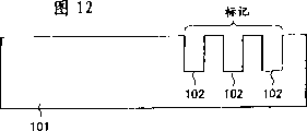
图12是表示与图3所示的实施形态1有关的存储单元的制造工序中标记形成工序的图。Fig. 12 is a view showing a mark forming step in the manufacturing process of the memory cell according to the first embodiment shown in Fig. 3 .
图13是表示同一制造工序的标记形成工序的图。Fig. 13 is a diagram showing a mark forming step in the same manufacturing process.
图14是表示同一制造工序的栅极(G2)形成工序的图。Fig. 14 is a diagram showing a gate (G2) forming step in the same manufacturing step.
图15是表示同一制造工序的衬底贴合工序的图。Fig. 15 is a diagram showing a substrate bonding step in the same manufacturing step.
图16是表示同一制造工序的衬底研磨工序的图。Fig. 16 is a diagram showing a substrate polishing step in the same manufacturing step.
图17是表示同一制造工序的栅极(G1)形成工序的图。Fig. 17 is a diagram showing a gate (G1) forming step in the same manufacturing step.
图18是表示同一制造工序的位线形成工序的图。FIG. 18 is a diagram showing a bit line forming step in the same manufacturing process.
图19是表示与图8所示的实施形态2有关的存储单元的制造工序中标记形成工序的图。Fig. 19 is a view showing a mark forming step in the manufacturing process of the memory cell according to the second embodiment shown in Fig. 8 .
图20是表示同一制造工序的标记形成工序的图。Fig. 20 is a diagram showing a mark forming step in the same manufacturing process.
图21是表示同一制造工序的栅极(G1)形成工序的图。Fig. 21 is a diagram showing a gate (G1) forming step in the same manufacturing step.
图22是表示同一制造工序的衬底贴合工序的图。Fig. 22 is a view showing a substrate bonding step in the same manufacturing step.
图23是表示同一制造工序的衬底研磨工序的图。Fig. 23 is a diagram showing a substrate polishing step in the same manufacturing step.
图24是表示同一制造工序的绝缘膜形成工序的图。FIG. 24 is a view showing an insulating film forming step in the same manufacturing process.
图25是表示同一制造工序的栅极(G2)形成工序的图。Fig. 25 is a diagram showing a gate (G2) forming step in the same manufacturing step.
图26是表示同一制造工序的位线形成工序的图。FIG. 26 is a diagram showing a bit line forming step in the same manufacturing process.
图27是表示与图9所示的实施形态3有关的存储单元的制造工序中标记形成工序的图。Fig. 27 is a view showing a mark forming step in the manufacturing process of the memory cell according to the third embodiment shown in Fig. 9 .
图28是表示同一制造工序的标记形成工序的图。Fig. 28 is a diagram showing a mark forming step in the same manufacturing process.
图29是表示同一制造工序的栅极(G2)形成工序的图。Fig. 29 is a view showing a gate (G2) forming step in the same manufacturing step.
图30是表示同一制造工序的衬底贴合工序的图。Fig. 30 is a diagram showing a substrate bonding step in the same manufacturing step.
图31是表示同一制造工序的衬底研磨工序的图。Fig. 31 is a diagram showing a substrate polishing step in the same manufacturing step.
图32是表示同一制造工序的栅极(G1)形成工序的图。Fig. 32 is a diagram showing a gate (G1) forming step in the same manufacturing step.
图33是表示同一制造工序的位线形成工序的图。FIG. 33 is a diagram showing a bit line forming step in the same manufacturing process.
图34A是表示与图10A到图10C所示的实施形态4有关的存储单元的制造工序中元件分离工序的图(在图10A中的A-A′线截面图)。Fig. 34A is a view showing an element isolation step in the manufacturing process of the memory cell according to Embodiment 4 shown in Figs. 10A to 10C (A-A' line sectional view in Fig. 10A).
图34B是表示与图10A到图10C所示的实施形态4有关的存储单元的制造工序中元件分离工序的图(在图10A中的B-B′线截面图)。Fig. 34B is a view showing an element isolation step in the manufacturing process of the memory cell according to Embodiment 4 shown in Figs. 10A to 10C (cross-sectional view taken along line B-B' in Fig. 10A).
图35A是表示同一制造工序的栅极埋入部分形成工序的图(图10A中的A-A′线截面图)。FIG. 35A is a view (cross-sectional view taken along line A-A' in FIG. 10A ) showing a gate embedding portion forming step in the same manufacturing process.
图35B是表示同一制造工序的栅极埋入部分形成工序的图(图10A中的B-B′线截面图)。FIG. 35B is a view (cross-sectional view taken along line B-B' in FIG. 10A ) showing a gate embedded portion forming step in the same manufacturing process.
图36A是表示同一制造工序的栅极(G1)埋入工序的图(图10A中的A-A′线截面图)。FIG. 36A is a view (cross-sectional view taken along line A-A' in FIG. 10A ) showing a gate (G1) embedding step in the same manufacturing process.
图36B是表示同一制造工序的栅极(G1)埋入工序的图(图10A中的B-B′线截面图)。FIG. 36B is a view (cross-sectional view taken along line B-B' in FIG. 10A ) showing a gate (G1) embedding step in the same manufacturing process.
图37A是表示同一制造工序的栅极(G2)形成工序的图(图10A中的A-A′线截面图)。FIG. 37A is a view (cross-sectional view taken along line A-A' in FIG. 10A ) showing a gate (G2) forming step in the same manufacturing process.
图37B是表示同一制造工序的栅极(G2)形成工序的图(图10A中的B-B′线截面图)。FIG. 37B is a view showing a gate (G2) forming step in the same manufacturing step (cross-sectional view taken along line B-B' in FIG. 10A ).
图38A是表示同一制造工序的固定电位线形成工序的图(图10A中的A-A′线截面图)。FIG. 38A is a view showing a fixed potential line forming step in the same manufacturing process (cross-sectional view taken along line A-A' in FIG. 10A ).
图38B是表示同一制造工序的固定电位线形成工序的图(图10A中的B-B′线截面图)。FIG. 38B is a view showing a fixed potential line forming step in the same manufacturing process (cross-sectional view taken along line B-B' in FIG. 10A ).
图39A是与图11的实施形态对应的单元阵列的布局图。Fig. 39A is a layout diagram of a cell array corresponding to the embodiment shown in Fig. 11 .
图39B是图39A的A-A′线截面图。Fig. 39B is a sectional view taken along line A-A' of Fig. 39A.
图39C是图39A的B-B′线截面图。Fig. 39C is a sectional view taken along line B-B' of Fig. 39A.
图40A是表示图39的单元阵列的制造工序中柱状硅形成工序的图(图39A中的A-A′线截面图)。40A is a view showing a columnar silicon formation step in the manufacturing process of the cell array of FIG. 39 (A-A' line sectional view in FIG. 39A ).
图40B是表示图39的单元阵列的制造工序中柱状硅形成工序的图(图39A中的B-B′线截面图)。40B is a view showing a columnar silicon formation step in the manufacturing process of the cell array of FIG. 39 (cross-sectional view taken along line B-B' in FIG. 39A ).
图41A是表示同一制造工序的柱状硅形成工序的图(图39A中的A-A′线截面图)。Fig. 41A is a diagram showing a columnar silicon formation step in the same manufacturing step (A-A' line sectional view in Fig. 39A).
图41B是表示同一制造工序的柱状硅形成工序的图(图39A中的B-B′线截面图)。FIG. 41B is a view showing a columnar silicon formation step in the same manufacturing process (cross-sectional view taken along line B-B' in FIG. 39A ).
图42A是表示同一制造工序的栅极材料淀积工序的图(图39A中的A-A′线截面图)。Fig. 42A is a diagram showing a gate material deposition step in the same manufacturing step (cross-sectional view taken along line A-A' in Fig. 39A).
图42B是表示同一制造工序的栅极材料淀积工序的图(图39A中的B-B′线截面图)。Fig. 42B is a diagram showing a gate material deposition step in the same manufacturing step (cross-sectional view taken along line B-B' in Fig. 39A).
图43A是表示同一制造工序的栅极形成工序的图(图39A中的A-A′线截面图)。FIG. 43A is a view showing a gate formation step in the same manufacturing process (cross-sectional view taken along line A-A' in FIG. 39A ).
图43B是表示同一制造工序的栅极形成工序的图(图39A中的B-B′线截面图)。FIG. 43B is a view (cross-sectional view taken along line B-B' in FIG. 39A ) showing a gate formation step in the same manufacturing process.
图44A是表示同一制造工序的平坦化工序的图(图39A中的A-A′线截面图)。FIG. 44A is a view showing a planarization step in the same manufacturing process (A-A' line sectional view in FIG. 39A ).
图44B是表示同一制造工序的平坦化工序的图(图39A中的B-B′线截面图)。FIG. 44B is a view showing a planarization step in the same manufacturing process (cross-sectional view taken along line B-B' in FIG. 39A ).
图45A是表示与图11所示的实施形态5有关的存储单元中其他单元阵列的布局图。Fig. 45A is a layout diagram showing another cell array in the memory cell according to the fifth embodiment shown in Fig. 11;
图45B是图45A的A-A′线截面图。Fig. 45B is a sectional view taken along line A-A' of Fig. 45A.
图45C是图45A的B-B′线截面图。Fig. 45C is a sectional view taken along line B-B' of Fig. 45A.
图46A是表示图45的单元阵列的制造工序中柱状硅形成工序的图(图45A中的A-A′线截面图)。46A is a view showing a columnar silicon formation step in the manufacturing process of the cell array of FIG. 45 (A-A' line sectional view in FIG. 45A ).
图46B是表示图45的单元阵列的制造工序中柱状硅形成工序的图(图45A中的B-B′线截面图)。46B is a view showing a columnar silicon formation step in the manufacturing process of the cell array of FIG. 45 (cross-sectional view taken along line B-B' in FIG. 45A ).
图47A是表示同一制造工序的柱状硅形成工序的图(图45A中的A-A′线截面图)。Fig. 47A is a diagram showing a columnar silicon formation step in the same manufacturing step (A-A' line sectional view in Fig. 45A).
图47B是表示同一制造工序的柱状硅形成工序的图(图45A中的B-B′线截面图)。FIG. 47B is a view showing a columnar silicon formation step in the same manufacturing process (cross-sectional view taken along line B-B' in FIG. 45A ).
图48A是表示同一制造工序的栅极材料淀积工序的图(图45A中的A-A′线截面图)。Fig. 48A is a diagram showing a gate material deposition step in the same manufacturing step (cross-sectional view taken along line A-A' in Fig. 45A).
图48B是表示同一制造工序的栅极材料淀积工序的图(图45A中的B-B′线截面图)。Fig. 48B is a diagram showing a gate material deposition step in the same manufacturing step (cross-sectional view taken along line B-B' in Fig. 45A).
图49A是表示同一制造工序的栅极(G1)形成工序的图(图45A中的A-A′线截面图)。FIG. 49A is a view (sectional view taken along line A-A' in FIG. 45A ) showing a gate (G1) forming step in the same manufacturing process.
图49B是表示同一制造工序的栅极(G1)形成工序的图(图45A中的B-B′线截面图)。FIG. 49B is a diagram showing a gate (G1) forming step in the same manufacturing step (cross-sectional view taken along line B-B' in FIG. 45A ).
图50A是表示同一制造工序的平坦化工序的图(图45A中的A-A′线截面图)。FIG. 50A is a view showing a planarization step in the same manufacturing process (A-A' line sectional view in FIG. 45A ).
图50B是表示同一制造工序的平坦化工序的图(图45A中的B-B′线截面图)。FIG. 50B is a view showing a planarization step in the same manufacturing process (cross-sectional view taken along line B-B' in FIG. 45A ).
图51A是表示同一制造工序的栅极(G2)形成区域的开口工序的图(图45A中的A-A′线截面图)。FIG. 51A is a view showing an opening step of a gate (G2) formation region in the same manufacturing process (cross-sectional view taken along line A-A' in FIG. 45A ).
图51B是表示同一制造工序的栅极(G2)形成区域的开口工序的图(图45A中的B-B′线截面图)。FIG. 51B is a view (cross-sectional view taken along line B-B' in FIG. 45A ) showing an opening process of a gate (G2) formation region in the same manufacturing process.
图52A是表示同一制造工序的栅极材料淀积工序的图(图45A中的A-A′线截面图)。Fig. 52A is a diagram showing a gate material deposition step in the same manufacturing step (cross-sectional view taken along line A-A' in Fig. 45A).
图52B是表示同一制造工序的栅极材料淀积工序的图(在图45A中的B-B′线截面图)。Fig. 52B is a view (cross-sectional view taken along line B-B' in Fig. 45A) showing a gate material deposition step in the same manufacturing process.
图53A是表示同一制造工序的栅极(G2)形成工序的图(图45A中的A-A′线截面图)。FIG. 53A is a view (sectional view taken along line A-A' in FIG. 45A ) showing a gate (G2) forming step in the same manufacturing process.
图53B是表示同一制造工序的栅极(G2)形成工序的图(图45A中的B-B′线截面图)。FIG. 53B is a view (cross-sectional view taken along line B-B' in FIG. 45A ) showing a gate (G2) forming step in the same manufacturing process.
图54A是表示图39A的实施形态中追加分路配线的实施形态的布局图。Fig. 54A is a layout diagram showing an embodiment in which shunt wiring is added to the embodiment in Fig. 39A.
图54B是图54A的A-A′线截面图。Fig. 54B is a sectional view taken along line A-A' of Fig. 54A.
图54C是图54A的B-B′线截面图。Fig. 54C is a sectional view taken along line B-B' of Fig. 54A.
图55A是当用其它分路配线构造时图54A的A-A′线截面图。Fig. 55A is a sectional view taken along line A-A' of Fig. 54A when other shunt wiring structures are used.
图55B是当用其它分路配线构造时图54A的B-B′线截面图。Fig. 55B is a sectional view taken along line B-B' of Fig. 54A when other shunt wiring structures are used.
图56是与图3对应地表示当将与实施形态1有关的n沟道型MIS晶体管变形为p沟道型时的存储单元构造的图。FIG. 56 is a diagram corresponding to FIG. 3 and showing the memory cell structure when the n-channel type MIS transistor according to
图57是与图8对应地表示当将与实施形态2有关的n沟道型MIS晶体管变形为p沟道型时的存储单元构造的图。Fig. 57 is a diagram corresponding to Fig. 8 and showing the memory cell structure when the n-channel type MIS transistor according to the second embodiment is modified into a p-channel type.
图58是与图9对应地表示当将与实施形态3有关的n沟道型MIS晶体管变形为p沟道型时的存储单元构造的图。Fig. 58 is a diagram corresponding to Fig. 9 and showing the memory cell structure when the n-channel type MIS transistor according to
图59A是与图10对应地表示当将与实施形态4有关的n沟道型MIS晶体管变形为p沟道型时的存储单元构造的图。FIG. 59A is a diagram corresponding to FIG. 10 and showing the structure of a memory cell when the n-channel type MIS transistor according to Embodiment 4 is modified into a p-channel type.
图59B是与图10C对应地表示当将与实施形态4有关的n沟道型MIS晶体管变形为p沟道型时的存储单元构造的图。FIG. 59B is a diagram corresponding to FIG. 10C and showing the structure of a memory cell when the n-channel MIS transistor according to Embodiment 4 is changed to a p-channel type.
图60A是与图11对应地表示当将与实施形态5有关的n沟道型MIS晶体管变形为p沟道型时的存储单元构造的图。FIG. 60A is a diagram corresponding to FIG. 11 and showing the memory cell structure when the n-channel type MIS transistor according to Embodiment 5 is modified into a p-channel type.
图60B是与图7A对应地表示当用p沟道型MIS晶体管时的驱动电压波形的图。FIG. 60B is a diagram corresponding to FIG. 7A and showing a driving voltage waveform when a p-channel type MIS transistor is used.
图60C是与图7B对应地表示当用p沟道型MIS晶体管时的驱动电压波形的图。FIG. 60C is a diagram corresponding to FIG. 7B and showing a driving voltage waveform when a p-channel type MIS transistor is used.
图61是表示用于图3实施形态的单元模拟的晶体管参数的图。Fig. 61 is a diagram showing transistor parameters used in the cell simulation of the embodiment shown in Fig. 3 .
图62是表示根据同一模拟写入“0”和其后的读出工作的电压波形的图。Fig. 62 is a diagram showing voltage waveforms of writing "0" and subsequent read operation according to the same simulation.
图63是表示根据同一模拟写入“1”和其后的读出工作的电压波形的图。Fig. 63 is a diagram showing voltage waveforms according to the same analog writing of "1" and the subsequent read operation.
图64是表示根据同一模拟写入“0”,“1”数据时单元的漏极电流-栅极电压特性的图。Fig. 64 is a graph showing drain current-gate voltage characteristics of a cell when "0" and "1" data are written according to the same simulation.
图65是表示根据使辅助栅极处于固定电位的模拟写入“0”和其后的读出工作的电压波形的图。Fig. 65 is a diagram showing voltage waveforms by analog writing of "0" with the auxiliary gate at a fixed potential and the subsequent read operation.
图66是表示根据同一模拟写入“1”和其后的读出工作的电压波形的图。Fig. 66 is a diagram showing voltage waveforms according to the same analog writing of "1" and the subsequent read operation.
图67是表示根据同一模拟写入“0”,“1”数据时单元的漏极电流-栅极电压特性的图。Fig. 67 is a graph showing drain current-gate voltage characteristics of a cell when "0" and "1" data are written according to the same simulation.
图68A是根据实施形态6的单元阵列的平面图。Fig. 68A is a plan view of a cell array according to
图68B是图68A的I-I′截面图。Fig. 68B is a sectional view taken along line I-I' of Fig. 68A.
图68C是图68A的II-II′截面图。Fig. 68C is a II-II' sectional view of Fig. 68A.
图69是表示同一实施形态的制造工序中在第1硅衬底上形成栅极材料膜的工序的截面图。Fig. 69 is a cross-sectional view showing a step of forming a gate material film on a first silicon substrate in the manufacturing process of the same embodiment.
图70是表示同一制造工序中在第2硅衬底上进行氢离子注入工序的截面图。Fig. 70 is a cross-sectional view showing a hydrogen ion implantation step on a second silicon substrate in the same manufacturing step.
图71是表示同一制造工序中衬底贴合工序的截面图。Fig. 71 is a cross-sectional view showing a substrate bonding step in the same manufacturing step.
图72是表示同一制造工序中贴合衬底厚度调整工序的图。Fig. 72 is a diagram showing a step of adjusting the thickness of a bonded substrate in the same manufacturing process.
图73A是表示同一制造工序中元件分离工序的平面图。Fig. 73A is a plan view showing an element isolation step in the same manufacturing process.
图73B是图73A的II-II′截面图。Fig. 73B is a II-II' sectional view of Fig. 73A.
图74是表示同一制造工序中用于虚设字线的绝缘膜淀积工序的截面图。Fig. 74 is a cross-sectional view showing an insulating film deposition process for a dummy word line in the same manufacturing process.
图75是表示同一制造工序中虚设字线形成工序和用虚设字线的辅助栅极分离工序的截面图。75 is a cross-sectional view showing a step of forming a dummy word line and a step of isolating an auxiliary gate using the dummy word line in the same manufacturing process.
图76是表示同一制造工序中硅氮化膜形成工序的截面图。Fig. 76 is a cross-sectional view showing a silicon nitride film forming step in the same manufacturing step.
图77是表示同一制造工序中将绝缘膜埋入分离沟的工序的截面图。Fig. 77 is a cross-sectional view showing a step of embedding an insulating film into a separation trench in the same manufacturing step.
图78是表示同一制造工序中除去硅氮化膜的工序的截面图。Fig. 78 is a cross-sectional view showing a step of removing a silicon nitride film in the same manufacturing step.
图79是表示同一制造工序中生长硅层的工序的截面图。Fig. 79 is a cross-sectional view showing a step of growing a silicon layer in the same manufacturing step.
图80是表示同一制造工序中除去虚设字线的工序的截面图。Fig. 80 is a cross-sectional view showing a step of removing dummy word lines in the same manufacturing process.
图81是表示同一制造工序中栅极绝缘膜形成工序和硅氮化膜形成工序的截面图。81 is a cross-sectional view showing a gate insulating film forming step and a silicon nitride film forming step in the same manufacturing process.
图82是表示同一制造工序中主栅极埋入工序的截面图。Fig. 82 is a cross-sectional view showing a main gate embedding step in the same manufacturing process.
图83是表示同一制造工序中硅氮化膜淀积工序的截面图。Fig. 83 is a cross-sectional view showing a silicon nitride film deposition step in the same manufacturing step.
图84A是表示同一制造工序中硅氮化膜刻蚀工序的平面图。Fig. 84A is a plan view showing a silicon nitride film etching step in the same manufacturing process.
图84B是图84A的I-I′截面图。Fig. 84B is an I-I' sectional view of Fig. 84A.
图85是表示同一制造工序的元件分离工序的平面图。Fig. 85 is a plan view showing an element isolation step in the same manufacturing process.
图86是表示同一制造工序中源极,漏极扩散层形成工序的截面图。Fig. 86 is a cross-sectional view showing a step of forming source and drain diffusion layers in the same manufacturing process.
图87是表示同一制造工序中层间绝缘膜形成工序的截面图。Fig. 87 is a cross-sectional view showing a step of forming an interlayer insulating film in the same manufacturing step.
图88是表示同一制造工序中源极配线埋入沟形成工序的截面图。Fig. 88 is a cross-sectional view showing a step of forming a source wiring embedded trench in the same manufacturing process.
图89是表示同一制造工序中源极配线埋入工序的截面图。Fig. 89 is a cross-sectional view showing a source wiring embedding step in the same manufacturing process.
图90是表示同一制造工序中层间绝缘膜形成工序的截面图。Fig. 90 is a cross-sectional view showing a step of forming an interlayer insulating film in the same manufacturing step.
图91是表示同一制造工序中位线接触孔和配线沟形成工序的截面图。Fig. 91 is a cross-sectional view showing a step of forming a bit line contact hole and a wiring trench in the same manufacturing process.
图92是与根据其它实施形态的单元阵列的图68B对应的截面图。FIG. 92 is a cross-sectional view corresponding to FIG. 68B of a cell array according to another embodiment.
具体实施方式Detailed ways
下面,我们参照附图说明与本发明有关的几个实施形态。首先,在说明具体的实施形态前,先说明下面述说的实施形态中使用的存储单元的基本原理。Hereinafter, several embodiments related to the present invention will be described with reference to the drawings. First, before describing specific embodiments, the basic principles of memory cells used in the embodiments described below will be described.
图1表示DRAM的单个存储单元的基本截面构造。存储单元MC由SOI构造的n沟道MIS晶体管构成。即,在硅衬底10上形成硅氧化膜11作为绝缘膜,用在这个硅氧化膜11上形成p型硅层12的SOI衬底。在这个SOI衬底的硅层12上,通过栅极氧化膜16形成栅极13,与栅极13自匹配地形成n型漏极扩散层14和n型源极扩散层15。FIG. 1 shows a basic cross-sectional structure of a single memory cell of a DRAM. Memory cell MC is composed of an n-channel MIS transistor having an SOI structure. That is, a
漏极扩散层14和源极扩散层15形成达到底部的硅氧化膜11的深度。所以,由p型硅层12构成的沟道体区域,如果用氧化膜实施沟道宽度方向(与图的纸面垂直的方向)上的分离,则底面和沟道宽度方向的侧面与其它部分绝缘分离,沟道长度方向形成pn结分离的浮动状态。The
这种由MIS晶体管构成构成的DRAM单元的工作原理利用是晶体管沟道体(与其它部分绝缘分离的p型硅层12)的多数载流子的空穴的积累状态。即,通过使晶体管工作在5极管区域,从漏极14流出大电流,在漏极14附近引起碰撞离子化。使由这个碰撞离子化产生的作为多数载流子的空穴保持在p型硅层12中,例如将这个空穴的积累状态取为数据“1”,将漏极14和p型硅层12之间的pn结作为正向偏压,将p型硅层12的空穴放出到漏极一侧的状态取为数据“0”。The working principle of this DRAM cell composed of MIS transistors utilizes the accumulated state of holes of majority carriers in the transistor channel body (p-
数据“0”,“1”是沟道体的电位差,作为MIS晶体管的阈值电压差存储起来。图2表示给予栅极的驱动电位VWL和体电位VB之间的关系。如图2所示通过空穴积累,体电位VB高的数据“1”状态的阈值电压Vth1比数据“0”状态的阈值电压Vth0低。为了保持在体内积累是多数载流子的空穴的“1”状态,必须在栅极13上加上负的体电压。这个数据保持状态,限于不进行逆数据的写入工作(消去),即便进行读出工作也不改变。即,与利用电容的电荷积累的1个晶体管/1个电容的DRAM不同,可以进行非破坏读出。The data "0", "1" is the potential difference of the channel body, which is stored as the threshold voltage difference of the MIS transistor. FIG. 2 shows the relationship between the drive potential VWL given to the gate and the body potential VB. As shown in FIG. 2 , the threshold voltage Vth1 in the data "1" state with a high body potential VB is lower than the threshold voltage Vth0 in the data "0" state due to hole accumulation. In order to maintain the "1" state in which holes, which are majority carriers, accumulate in the body, a negative body voltage must be applied to the
在以上基本的DRAM单元构成中,是否能够只使数据“0”,“1”的阈值电压差中哪一个变大成为重要的问题。如从上述工作原理可以看到的那样,通过来自栅极13的电容耦合控制体电位,决定数据的写入特性和保持特性。可是,因为对于体电位阈值电压大致以平方根起作用,所以要实现数据“0”,“1”之间大的阈值电压差是不容易的。而且,在上述写入工作中,写入“0”的存储单元MC进行3极管工作,所以当形成沟道时栅极13和沟道体没有电容耦合,不能够使体电位上升。In the above basic DRAM cell configuration, whether or not it is possible to increase the threshold voltage difference between data "0" and "1" is an important issue. As can be seen from the above-described operation principle, the bulk potential is controlled by the capacitive coupling from the
因此在下面的实施形态中,除了对于上述的基本存储单元构造,设置用于形成沟道的主栅极(第1栅极)外,还对于MIS晶体管的沟道体设置用于通过电容耦合控制体电位的辅助栅极(第2栅极)。而且,通过与第1栅极同步地驱动第2栅极,可以实现更确实的数据写入,并且可以存储阈值电压差大的数据“0”,“1”。Therefore, in the following embodiments, in addition to providing the main gate (first gate) for forming a channel for the above-mentioned basic memory cell structure, the channel body of the MIS transistor is also provided for controlling by capacitive coupling. Auxiliary grid (second grid) for body potential. Furthermore, by driving the second gate synchronously with the first gate, more reliable data writing can be realized, and data "0" and "1" having a large threshold voltage difference can be stored.
下面我们说明具体的实施形态。Below we describe the specific implementation form.
[实施形态][implementation form]
图3与图1的基本构造对应地表示根据实施形态1的存储单元MC的构造。与图1不同之处在于除了是用于晶体管沟道控制的前栅极的第1栅极(G1)13外,还设置了用于控制体电位的第2栅极(G2)20。在本实施形态中,第2栅极20作为通过栅极绝缘膜19与硅层12的底面进行电容耦合的相对的后栅极,埋入硅层12下面的氧化膜11内。FIG. 3 shows the structure of the memory cell MC according to
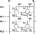
图4表示用多个这样的存储单元MC进行矩阵配列的存储单元阵列的等效电路图。并列在一个方向上的多个存储单元MC的第1栅极(G1)13与第1字线WL1连接,第2栅极(G2)20与第2字线WL2连接。在与这些字线WL1,WL2交叉的方向上,配置与存储单元MC的漏极连接的位线BL。所有的存储单元MC的源极15都与固定电位线(接地电位线VSS)连接。FIG. 4 shows an equivalent circuit diagram of a memory cell array in which a plurality of such memory cells MC are arranged in a matrix. The first gates ( G1 ) 13 of the plurality of memory cells MC arranged in one direction are connected to the first word line WL1 , and the second gates ( G2 ) 20 are connected to the second word line WL2 . A bit line BL connected to the drain of the memory cell MC is arranged in a direction intersecting with these word lines WL1 and WL2.
图5表示存储单元阵列的布局,图6A和图6B分别表示图5的A-A′线截面图和B-B′线截面图。p型硅层12通过埋入硅氧化膜21形成格子状的图案。即共有漏极14的2个晶体管的区域在字线WL1,WL2的方向上由硅氧化膜21进行分离元件地配列。或者代替埋入硅氧化膜21,也可以通过对硅层12进行刻蚀,实施横方向上的元件分离。在一个方向上连续地形成第1栅极13和第2栅极20,使它们成为字线WL1,WL2。在字线WL1,WL2的方向上连续地形成源极15,使它成为固定电位线(共同的源线)。在晶体管上覆盖层间绝缘膜17,在层间绝缘膜17上形成位线(BL)18。位线18与2个晶体管共有的漏极14接触,与字线WL1,WL2交叉那样地进行配置。5 shows a layout of a memory cell array, and FIGS. 6A and 6B show a cross-sectional view along line A-A' and a cross-sectional view along line B-B' of FIG. 5, respectively. The p-
因此,作为各晶体管的沟道体的硅层12在底面和沟道宽度方向的侧面由氧化膜相互分离,在沟道长方向由pn结相互分离,保持在浮动状态中。Therefore, the
而且在这种存储单元阵列构成中,通过以最小加工尺寸F的间隔形成字线WL1,WL2和位线BL,单个单元面积如图5的虚线所示,成为2F×2F=4F2。Furthermore, in this memory cell array structure, by forming word lines WL1, WL2 and bit line BL at intervals of the minimum processing size F, the area of a single cell becomes 2F×2F=4F 2 as shown by the dotted line in FIG. 5 .
如上所述,将一个MIS晶体管作为1比特的存储单元MC,构成能够进行定时存储的存储单元阵列。As described above, one MIS transistor is used as a 1-bit memory cell MC to constitute a memory cell array capable of timing storage.
图7A和图7B表示写入数据时的字线WL1,WL2和位线BL的电压波形图。同步地驱动成对的第1字线WL1和第2字线WL2。图7A是当用相同材料构成第1栅极13和第2栅极20时,通过将第2栅极20控制在比第1栅极13低的电位上,在沟道体的第2栅极20一侧可以积累多数载流子。另一方面,图7B是当用功函数不同的电极材料构成第1栅极13和第2栅极20时,通过给予两者相同的电位,在沟道体的第2栅极20一侧可以积累多数载流子。7A and 7B show voltage waveforms of word lines WL1, WL2 and bit line BL when writing data. The paired first word line WL1 and second word line WL2 are driven synchronously. FIG. 7A shows that when the
在图7A的情形中,当写入数据“1”时,将比基准电位VSS高的正电位VWL1H给予选出的第1字线WL1,同时将比这个电位低的电位VWL2H(在图例中比基准电位VSS低的负电位)给予选出的第2字线WL2,将比基准电位VSS高的正电位VBLH给予选出的位线BL。因此,在选出的存储单元MC中,产生由5极管工作引起的碰撞离子化,在沟道体中积累空穴。In the case of FIG. 7A, when data "1" is written, a positive potential VWL1H higher than the reference potential VSS is given to the selected first word line WL1, and a potential VWL2H lower than this potential (referred to in the illustration as A negative potential lower than the reference potential VSS is given to the selected second word line WL2, and a positive potential VBLH higher than the reference potential VSS is given to the selected bit line BL. Therefore, in the selected memory cell MC, impact ionization due to the operation of the pentode occurs, and holes are accumulated in the channel body.
数据保持是将比基准电位VSS低的负电位VWL1L给予第1字线WL1,并将比这个电位更低的低电位VWL2L给予选出的第2字线WL2。因此,保持表示在沟道体中积累过剩空穴状态的数据“1”。To hold data, a negative potential VWL1L lower than the reference potential VSS is given to the first word line WL1, and a low potential VWL2L lower than this potential is given to the selected second word line WL2. Therefore, data "1" indicating a state of excess holes accumulated in the channel body is maintained.
当写入数据“0”时,分别将与写入数据“1”时相同的电位VWL1H和VWL2H给予选出的第1和第2字线WL1和WL2,并将比基准电位VSS低的负电位VBLL给予选出的位线BL。因此,在选出的存储单元MC中,漏结处于顺偏压,将沟道体中的空穴排出到漏极14,写入表示体电位低的状态的数据“0”。When writing data "0", the same potentials VWL1H and VWL2H as when writing data "1" are respectively given to the selected first and second word lines WL1 and WL2, and a negative potential lower than the reference potential VSS VBLL is given to the selected bit line BL. Therefore, in the selected memory cell MC, the drain junction is forward-biased, the holes in the channel body are discharged to the
在图7B的情形中,当写入数据“1”时,将比基准电位VSS高的正电位VWLH给予选出的第1和第2字线WL1和VW2,将比基准电位VSS高的正电位VBLH给予选出的位线BL。因此,在选出的存储单元MC中,产生由5极管工作引起的碰撞离子化,在沟道体中积累空穴。In the case of FIG. 7B, when writing data "1", the positive potential VWLH higher than the reference potential VSS is given to the selected first and second word lines WL1 and VW2, and the positive potential VWLH higher than the reference potential VSS is given to the selected first and second word lines WL1 and VW2. VBLH is given to the selected bit line BL. Therefore, in the selected memory cell MC, impact ionization due to the operation of the pentode occurs, and holes are accumulated in the channel body.
数据保持是将比基准电位VSS低的负电位VWLL给予第1和第2字线WL1和WL2。因此,保持表示在沟道体中积累过剩空穴的状态的数据“1”。To hold data, negative potential VWLL lower than reference potential VSS is given to first and second word lines WL1 and WL2. Therefore, data "1" indicating a state in which excess holes are accumulated in the channel body is maintained.
当写入数据“0”时,分别将与写入数据“1”时相同的电位VWLH给予选出的第1和第2字线WL1和WL2,将比基准电位VSS低的负电位VBLL给予选出的位线BL。因此,在选出的存储单元MC中,漏结处于顺偏压,将沟道体中的空穴排出到漏极14,写入表示体电位低的状态的数据“0”。When data "0" is written, the same potential VWLH as when data "1" is written is given to the selected first and second word lines WL1 and WL2, and a negative potential VBLL lower than the reference potential VSS is given to the selected word line. out the bit line BL. Therefore, in the selected memory cell MC, the drain junction is forward-biased, the holes in the channel body are discharged to the
这样,如果用功函数不同的材料构成2个栅极13和20,则通过用相同的电位同步驱动第1字线WL1和第2字线WL2,能够控制到沟道体的空穴积累。Thus, if the two
在以上那样的这个实施形态中,通过与主栅极(第1栅极)13一起驱动辅助栅极(第2栅极)20,能够写入阈值电压差大的数据“0”,“1”。即,在第2栅极20上加上负电位处于数据保持状态,很好地保持数据“1”的空穴积累状态,同时通过当写入数据时提高这个第2栅极20的电位,由于电容耦合使体电位上升,能够确实地写入数据。In this embodiment as above, by driving the auxiliary gate (second gate) 20 together with the main gate (first gate) 13, data "0" and "1" with a large threshold voltage difference can be written. . That is, a negative potential is applied to the
当写入数据“0”时,即便在第1栅极13一侧形成沟道,因为通过驱动第2栅极20能够使体电位上升,所以可以确实地写入数据“0”。When data "0" is written, even if a channel is formed on the
由于上述情况,能够存储阈值电压差大的数据“0”,“1”。Due to the above, data "0", "1" with a large threshold voltage difference can be stored.
又,通过降低非选出的第1字线WL1的电位进行数据保持,但是因为这时成对的第2字线WL2的电位也下降向下控制体电位,所以在与相同位线BL连接的其它单元中进行数据“0”的写入时,能够确实地防止破坏在保持数据“1”的非选出的存储单元MC中的数据。进一步,在与写入“1”的位线BL连接的非选出的数据“0”单元中,存在着由于表面电压击穿和GIDL(Gate Induced Drain Leakage,栅极感应漏极泄漏)电流引起数据破坏的悬念,但是在本实施形态的情形中,通过降低第2字线WL2的体电位,也能够解除这些悬念。Also, data is held by lowering the potential of the unselected first word line WL1. However, at this time, the potential of the paired second word line WL2 is also lowered to control the bulk potential. When data "0" is written in other cells, data in non-selected memory cells MC holding data "1" can be reliably prevented from being destroyed. Further, in the non-selected data "0" cell connected to the bit line BL written "1", there is a current caused by surface voltage breakdown and GIDL (Gate Induced Drain Leakage, Gate Induced Drain Leakage) However, in the case of this embodiment, these concerns can also be resolved by lowering the bulk potential of the second word line WL2.
进一步,当写入“0”时,使位线BL的电位很大下降,从源极15到位线BL流动着电流,但是在本实施形态的情形中,因为由于第2栅极20使体电位上升,所以不需要使位线BL有这种程度的下降。因此,例如,可以使位线BL的电位与源极的基准电位VSS大致相同,从而能够抑制从源极15到位线BL流动的电流。Furthermore, when "0" is written, the potential of the bit line BL is greatly lowered, and a current flows from the
又当读出数据时,为了不会错误地写入“1”,需要进行3极管工作。因此,位线BL的电位比写入“1”时的低,但是因此在漏极14和沟道体之间的耗散层的伸展比写入“1”时小,从而使位线BL和沟道体之间的电容耦合变大。这成为写入时使注入沟道体的载流子进行电容再分配,体电位下降的原因。在本实施形态中,由于第2栅极20的控制,能够很好地保持沟道体的多数载流子积累状态。When reading data, in order not to write "1" by mistake, it is necessary to perform triode operation. Therefore, the potential of the bit line BL is lower than when "1" is written, but therefore the extension of the dissipation layer between the
其次,我们说明在本实施形态中行译码器和字线驱动器的具体电路构成的一个例子。图7C是行译码器的一个例子,是表示用于产生图7B所示的字线WL1,WL2的电压波形的字线驱动器WDDV1的一个例子的图。Next, an example of the specific circuit configuration of the row decoder and the word line driver in this embodiment will be described. FIG. 7C is an example of a row decoder, and is a diagram showing an example of word line driver WDDV1 for generating voltage waveforms of word lines WL1 and WL2 shown in FIG. 7B.
如这个图7C所示,行译码器RDEC由NAND电路C10构成,字线驱动器WDDV1由反相电路C11,电平变换电路C12,电平变换电路C13,和输出缓冲电路C14构成。通过这种构成,由行译码器RDEC选出的字线驱动器WDDV1将高电平的电位变换成比正电位VCC高的电位VWLH,供给字线WL1,WL2。As shown in this FIG. 7C, the row decoder RDEC is composed of a NAND circuit C10, and the word line driver WDDV1 is composed of an inverter circuit C11, a level conversion circuit C12, a level conversion circuit C13, and an output buffer circuit C14. With this configuration, the word line driver WDDV1 selected by the row decoder RDEC converts the high-level potential to a potential VWLH higher than the positive potential VCC, and supplies the potential to the word lines WL1 and WL2.
更具体地,将行地址信号RADD和字线启动信号WLEN输入NAND电路C10。将所有的高电平的行地址信号RADD和高电平的字线启动信号WLEN输入与选出的字线WL1,WL2对应的字线驱动器WDDV1。所以,与选出的字线WL1,WL2对应的字线驱动器WDDV1的NAND电路C10的输出成为低电平,即基准电位VSS。将NAND电路C10的输出输入到反相电路C11。More specifically, a row address signal RADD and a word line enable signal WLEN are input to the NAND circuit C10. All the high-level row address signal RADD and the high-level word line enable signal WLEN are input to the word line driver WDDV1 corresponding to the selected word lines WL1 and WL2. Therefore, the output of the NAND circuit C10 of the word line driver WDDV1 corresponding to the selected word lines WL1 and WL2 becomes low level, that is, the reference potential VSS. The output of the NAND circuit C10 is input to the inverter circuit C11.
这个反相电路C11反转输入的信号并输出。所以,在选出的字线驱动器WDDV1中,反相电路C11的输出成为高电平,即正的电位VCC。将这个反相电路C11的输出输入到电平变换电路C12和电平变换电路C13。又,也将NAND电路C10的输出输入到电平变换电路C12和电平变换电路C13。This inverting circuit C11 inverts the input signal and outputs it. Therefore, in the selected word line driver WDDV1, the output of the inverter circuit C11 becomes a high level, that is, a positive potential VCC. The output of this inverter circuit C11 is input to a level conversion circuit C12 and a level conversion circuit C13. In addition, the output of the NAND circuit C10 is also input to the level conversion circuit C12 and the level conversion circuit C13.
将这个电平变换电路C12和电平变换电路C13的输出输入到输出缓冲电路C14。通过电平变换电路C12和输出缓冲电路C14将是反相电路C11的高电平输出电位VCC的输出变换成比VCC高的正电位VWLH,供给字线WL1,WL2。又,通过电平变换电路C13和输出缓冲电路C14,将反相电路C11的低电平输出电位VSS的输出变换成比VSS低的电位VWLL,供给字线WL1,WL2。The outputs of the level conversion circuit C12 and the level conversion circuit C13 are input to the output buffer circuit C14. The output of the high-level output potential VCC of the inverter circuit C11 is converted into a positive potential VWLH higher than VCC by the level conversion circuit C12 and the output buffer circuit C14, and supplied to the word lines WL1 and WL2. Furthermore, the output of the low-level output potential VSS of the inverter circuit C11 is converted into a potential VWLL lower than VSS by the level conversion circuit C13 and the output buffer circuit C14, and supplied to the word lines WL1 and WL2.
在本实施形态中,电平变换电路C12通过备有p型MOS晶体管PM10,PM11和n型MOS晶体管NM10,NM11构成。p型MOS晶体管PM10,PM11的源极端子分别与电位VWLH的供给线连接,其漏极端子分别与n型MOS晶体管NM10,NM11的漏极端子连接。又,p型MOS晶体管PM10的栅极端子与在p型MOS晶体管PM11和n型MOS晶体管NM11之间的节点连接,p型MOS晶体管PM11的栅极端子与在p型MOS晶体管PM10和n型MOS晶体管NM10之间的节点连接。In this embodiment, the level conversion circuit C12 is constituted by including p-type MOS transistors PM10, PM11 and n-type MOS transistors NM10, NM11. Source terminals of p-type MOS transistors PM10 and PM11 are connected to a supply line of potential VWLH, respectively, and drain terminals thereof are connected to drain terminals of n-type MOS transistors NM10 and NM11, respectively. Also, the gate terminal of the p-type MOS transistor PM10 is connected to a node between the p-type MOS transistor PM11 and the n-type MOS transistor NM11, and the gate terminal of the p-type MOS transistor PM11 is connected to the node between the p-type MOS transistor PM10 and the n-type MOS transistor NM11. Node connection between transistors NM10.
将反相电路C11的输出输入到n型MOS晶体管NM10的栅极端子,将NAND电路C10的输出输入到n型MOS晶体管NM11的栅极端子。这些n型MOS晶体管NM10,NM11的源极端子分别与电位VSS的供给线连接。另一方面,电平变换电路C13通过备有p型MOS晶体管PM12,PM13和n型MOS晶体管NM12,NM14构成。p型MOS晶体管PM12,PM13的源极端子分别与电位VCC的供给线连接,其漏极端子分别与n型MOS晶体管NM12,NM13的漏极端子连接。又,将反相电路C11的输出输入到p型MOS晶体管PM12的栅极端子,将NAND电路C10的输出输入到p型MOS晶体管PM13的栅极端子。The output of the inverter circuit C11 is input to the gate terminal of the n-type MOS transistor NM10, and the output of the NAND circuit C10 is input to the gate terminal of the n-type MOS transistor NM11. Source terminals of these n-type MOS transistors NM10 and NM11 are respectively connected to a supply line of potential VSS. On the other hand, the level conversion circuit C13 is constituted by including p-type MOS transistors PM12, PM13 and n-type MOS transistors NM12, NM14. Source terminals of p-type MOS transistors PM12 and PM13 are connected to the supply line of potential VCC, respectively, and drain terminals thereof are connected to drain terminals of n-type MOS transistors NM12 and NM13, respectively. Also, the output of the inverter circuit C11 is input to the gate terminal of the p-type MOS transistor PM12, and the output of the NAND circuit C10 is input to the gate terminal of the p-type MOS transistor PM13.
n型MOS晶体管NM12的栅极端子与在p型MOS晶体管PM13和n型MOS晶体管NM13之间的节点连接,n型MOS晶体管NM13的栅极端子与在p型MOS晶体管PM12和n型MOS晶体管NM12之间的节点连接。又,这些n型MOS晶体管NM12,NM13的源极端子分别与电位VWLL的供给线连接。The gate terminal of n-type MOS transistor NM12 is connected to a node between p-type MOS transistor PM13 and n-type MOS transistor NM13, and the gate terminal of n-type MOS transistor NM13 is connected to a node between p-type MOS transistor PM12 and n-type MOS transistor NM12. Node connections between. Also, source terminals of these n-type MOS transistors NM12 and NM13 are respectively connected to supply lines of potential VWLL.
输出缓冲电路C14是通过将p型MOS晶体管PM14,PM15和n型MOS晶体管NM14,NM15串联地连接起来构成的。Output buffer circuit C14 is formed by connecting p-type MOS transistors PM14, PM15 and n-type MOS transistors NM14, NM15 in series.
p型MOS晶体管PM14的源极端子与电位VWLH的供给线连接,其栅极端子与在电平变换电路C12中的p型MOS晶体管PM11的栅极端子连接。p型MOS晶体管PM14的漏极端子与p型MOS晶体管PM15的源极端子连接。将电位VSS输入到这个p型MOS晶体管PM15的栅极端子。因此,p型MOS晶体管PM15成为常通的MOS晶体管。又,p型MOS晶体管PM15的漏极端子与n型MOS晶体管NM14的漏极端子连接。从这些p型MOS晶体管PM15和n型MOS晶体管NM14之间的节点输出用于驱动字线WL1,WL2的电压。The source terminal of the p-type MOS transistor PM14 is connected to the supply line of the potential VWLH, and the gate terminal thereof is connected to the gate terminal of the p-type MOS transistor PM11 in the level conversion circuit C12. The drain terminal of the p-type MOS transistor PM14 is connected to the source terminal of the p-type MOS transistor PM15. The potential VSS is input to the gate terminal of this p-type MOS transistor PM15. Therefore, the p-type MOS transistor PM15 becomes a normally-on MOS transistor. Also, the drain terminal of the p-type MOS transistor PM15 is connected to the drain terminal of the n-type MOS transistor NM14. A voltage for driving word lines WL1, WL2 is output from a node between these p-type MOS transistor PM15 and n-type MOS transistor NM14.
将电位VCC供给n型MOS晶体管NM14的栅极端子。因此,n型MOS晶体管NM14的栅极端子成为常通的MOS晶体管。n型MOS晶体管NM14的源极端子与n型MOS晶体管NM15的漏极端子连接。这个n型MOS晶体管NM15的栅极端子与在电平变换电路C13中的n型MOS晶体管NM13的栅极端子连接。又,n型MOS晶体管NM15的源极端子与电位VWLL的供给线连接。The potential VCC is supplied to the gate terminal of the n-type MOS transistor NM14. Therefore, the gate terminal of the n-type MOS transistor NM14 becomes a normally-on MOS transistor. The source terminal of n-type MOS transistor NM14 is connected to the drain terminal of n-type MOS transistor NM15. The gate terminal of this n-type MOS transistor NM15 is connected to the gate terminal of the n-type MOS transistor NM13 in the level conversion circuit C13. Also, the source terminal of n-type MOS transistor NM15 is connected to a supply line of potential VWLL.
用如上构成的行译码器RDEC和字线驱动器WDDV1,产生图7B所示的电位VWLH,VWLL,供给字线WL1,WL2。此外,在图7C中,在各MOS晶体管上实施后栅极连接,但是不一定需要这样做。With row decoder RDEC and word line driver WDDV1 configured as above, potentials VWLH, VWLL shown in FIG. 7B are generated and supplied to word lines WL1, WL2. Also, in FIG. 7C, gate-back connections are implemented on each MOS transistor, but this is not necessarily required.
此外,这个字线驱动器WDDV1的输出缓冲电路C14备有常通的MOS晶体管PM15,NM14,但是这是为了不将电位VWLH和电位VWLL的电位差直接加到MOS晶体管PM14,NM15上。即,通过常通的MOS晶体管PM15,NM14,电位差只减少与这个阈值下降相当的电压。所以,如果也可以将这个电位差直接加到MOS晶体管PM14,PM15上,则如图7D所示,也可以省略MOS晶体管PM15,NM14。In addition, the output buffer circuit C14 of the word line driver WDDV1 includes normally-on MOS transistors PM15 and NM14, but this is for not directly applying the potential difference between the potential VWLH and the potential VWLL to the MOS transistors PM14 and NM15. That is, the potential difference is reduced by the voltage corresponding to this threshold drop by the normally-on MOS transistors PM15 and NM14. Therefore, if this potential difference can also be directly applied to the MOS transistors PM14, PM15, as shown in FIG. 7D, the MOS transistors PM15, NM14 can also be omitted.
将这些图7C或图7D所示的行译码器RDEC和字线驱动器WDDV1配置在存储单元阵列MCA上的布局图如图7E所示。如这个图7E所示,当字线驱动器WDDV1的布局间隔与字线WL1,WL2的配线间隔一致时,能够将行译码器RDEC和字线驱动器WDDV1配置在存储单元阵列MCA的一侧。FIG. 7E shows a layout of row decoder RDEC and word line driver WDDV1 shown in FIG. 7C or 7D arranged on memory cell array MCA. As shown in FIG. 7E, when the layout interval of word line driver WDDV1 matches the wiring interval of word lines WL1 and WL2, row decoder RDEC and word line driver WDDV1 can be arranged on one side of memory cell array MCA.
与此相对,当字线驱动器WDDV1的布局面积增大,能够使字线驱动器WDDV1的布局间隔与字线WL1,WL2的配线间隔不一致时,可以考虑如图7F所示的布局。即,将行译码器RDEC和字线驱动器WDDV1配置在存储单元阵列MCA的两侧,例如,用在存储单元阵列MCA左侧的行译码器RDEC和字线驱动器WDDV1驱动奇数号码的字线WL1,WL2的译码,用在存储单元阵列MCA右侧的行译码器RDEC和字线驱动器WDDV1驱动偶数号码的字线WL1,WL2的译码。On the other hand, when the layout area of the word line driver WDDV1 is increased and the layout interval of the word line driver WDDV1 can be made different from the wiring intervals of the word lines WL1 and WL2, the layout shown in FIG. 7F can be considered. That is, the row decoder RDEC and the word line driver WDDV1 are arranged on both sides of the memory cell array MCA, for example, the row decoder RDEC and the word line driver WDDV1 on the left side of the memory cell array MCA are used to drive odd-numbered word lines The decoding of WL1 and WL2 is performed by using the row decoder RDEC and the word line driver WDDV1 on the right side of the memory cell array MCA to drive the decoding of even numbered word lines WL1 and WL2.
其次,我们说明与图7A对应的行数据和字线驱动器的电路构成。图7G是行译码器的一个例子,是表示用于产生图7A所示的字线WL1,WL2的电压波形的字线驱动器WDDV2的一个例子的图。Next, we describe the circuit configuration of the row data and word line drivers corresponding to FIG. 7A. FIG. 7G is an example of a row decoder, and is a diagram showing an example of word line driver WDDV2 for generating voltage waveforms of word lines WL1 and WL2 shown in FIG. 7A.
如这个图7G所示,行译码器RDEC由NAND电路C10构成,字线驱动器WDDV2由反相电路C11,电平变换电路C22,电平变换电路C23,输出缓冲电路C24,电平变换电路C25和输出缓冲电路C26构成。这里的电压高低关系,按照图7A的例子,为VWL1H>VSS>VWL2H>VWL1L>VWL2L。As shown in FIG. 7G, the row decoder RDEC is composed of a NAND circuit C10, and the word line driver WDDV2 is composed of an inverter circuit C11, a level conversion circuit C22, a level conversion circuit C23, an output buffer circuit C24, and a level conversion circuit C25. and the output buffer circuit C26. Here, the voltage level relationship, according to the example in FIG. 7A , is VWL1H>VSS>VWL2H>VWL1L>VWL2L.
当只说明与图7C不同之处时,电平变换电路C22具有基本上与图7C的电平变换电路C12相同的构成,备有p型MOS晶体管PM20,PM21和n型MOS晶体管NM20,NM21。但是,p型MOS晶体管PM20,PM21的源极端子与电位VWL1H的供给线连接。When only the differences from FIG. 7C are described, level shift circuit C22 has basically the same configuration as level shift circuit C12 in FIG. 7C, and includes p-type MOS transistors PM20, PM21 and n-type MOS transistors NM20, NM21. However, the source terminals of the p-type MOS transistors PM20 and PM21 are connected to the supply line of the potential VWL1H.
电平变换电路C23也具有基本上与图7C的电平变换电路C13相同的构成,备有p型MOS晶体管PM22,PM23和n型MOS晶体管NM22,NM23。但是,n型MOS晶体管NM22,NM23的源极端子与电位VWL1L的供给线连接。Level shift circuit C23 also has basically the same configuration as level shift circuit C13 in FIG. 7C, and includes p-type MOS transistors PM22, PM23 and n-type MOS transistors NM22, NM23. However, the source terminals of n-type MOS transistors NM22 and NM23 are connected to the supply line of potential VWL1L.
输出缓冲电路C24也具有基本上与图7C的输出缓冲电路C14相同的构成,备有串联连接的p型MOS晶体管PM24,PM25和n型MOS晶体管NM24,NM25。但是,p型MOS晶体管PM24的源极端子与电位VWL1H的供给线连接,n型MOS晶体管NM25的源极端子与电位VWL1L的供给线连接。The output buffer circuit C24 also has basically the same configuration as the output buffer circuit C14 of FIG. 7C, and includes p-type MOS transistors PM24, PM25 and n-type MOS transistors NM24, NM25 connected in series. However, the source terminal of the p-type MOS transistor PM24 is connected to the supply line of the potential VWL1H, and the source terminal of the n-type MOS transistor NM25 is connected to the supply line of the potential VWL1L.
此外,图7G的字线驱动器WDDV2备有电平变换电路C25和输出缓冲电路C26。电平变换电路C25的构成与电平变换电路C23的构成相同,备有p型MOS晶体管PM26,PM27和n型MOS晶体管NM26,NM27。但是,n型MOS晶体管NM26,NM27的源极端子与电位VWL2L的供给线连接。In addition, the word line driver WDDV2 in FIG. 7G includes a level conversion circuit C25 and an output buffer circuit C26. The configuration of the level conversion circuit C25 is the same as that of the level conversion circuit C23, and includes p-type MOS transistors PM26, PM27 and n-type MOS transistors NM26, NM27. However, source terminals of n-type MOS transistors NM26 and NM27 are connected to a supply line of potential VWL2L.
输出缓冲电路C26具有与输出缓冲电路C24相同的构成,但是由p型MOS晶体管PM28和n型MOS晶体管NM28这样2个MOS晶体管构成。而且,p型MOS晶体管PM28的源极端子与电位VWL2H的供给线连接,n型MOS晶体管NM28的源极端子与电位VWL2L的供给线连接。The output buffer circuit C26 has the same configuration as the output buffer circuit C24, but is composed of two MOS transistors, a p-type MOS transistor PM28 and an n-type MOS transistor NM28. Furthermore, the source terminal of the p-type MOS transistor PM28 is connected to the supply line of the potential VWL2H, and the source terminal of the n-type MOS transistor NM28 is connected to the supply line of the potential VWL2L.
不插入常通MOS晶体管的原因是,如从图7A可以看到的那样,因为电位VWL2H和电位VWL2L之间的电位差没有大到这种程度,所以即便将这个电位差直接加到MOS晶体管PM28,NM28上,也不会发生问题。The reason why the normally-on MOS transistor is not inserted is that, as can be seen from FIG. 7A, since the potential difference between the potential VWL2H and the potential VWL2L is not so large, even if this potential difference is directly applied to the MOS transistor PM28 , NM28, the problem will not occur.
如从这种构成可以看到的那样,输出缓冲电路C24的输出,在电位VWL1H和电位VWL1L之间振荡,因此,驱动第1字线WL1。又,输出缓冲电路C26的输出,在电位VWL2H和电位VWL2L之间,与输出缓冲电路C24的输出同步地振荡,因此,驱动第2字线WL2。此外,在图7G中,在各MOS晶体管中实施后栅极连接,但是不一定需要这样做。As can be seen from this configuration, the output of the output buffer circuit C24 oscillates between the potential VWL1H and the potential VWL1L, thereby driving the first word line WL1. Furthermore, the output of the output buffer circuit C26 oscillates between the potential VWL2H and the potential VWL2L in synchronization with the output of the output buffer circuit C24, thereby driving the second word line WL2. Furthermore, in FIG. 7G , gate-back connection is implemented in each MOS transistor, but this is not necessarily required.
又,与图7D所示的字线驱动器WDDV1相同,即便在图7H所示的字线驱动器WDDV2中,也可以省略p型MOS晶体管PM25和n型MOS晶体管NM24。Also, like word line driver WDDV1 shown in FIG. 7D , p-type MOS transistor PM25 and n-type MOS transistor NM24 can be omitted also in word line driver WDDV2 shown in FIG. 7H .
将这些图7G或图7H所示的行译码器RDEC和字线驱动器WDDV2配置在存储单元阵列MCA上的布局图如图7I所示。在如图7G和图7H所示的字线驱动器WDDV2中,根据用不同的电位同步地驱动第1字线WL1和第2字线WL2的关系,这个布局面积比图7C和图7D所示的字线驱动器WDDV1大。所以,我们考虑要使字线驱动器WDDV2的布局间隔与字线WL1,WL2的配线间隔一致是困难的。因此,在图7I所示的布局中,将行译码器RDEC和字线驱动器WDDV2配置在存储单元阵列MCA的两侧,例如,用在存储单元阵列MCA左侧的行译码器RDEC和字线驱动器WDDV2驱动奇数号码的字线WL1,WL2的译码,用在存储单元阵列MCA右侧的行译码器RDEC和字线驱动器WDDV2驱动偶数号码的字线WL1,WL2的译码。FIG. 7I shows a layout of row decoder RDEC and word line driver WDDV2 shown in FIG. 7G or FIG. 7H arranged on memory cell array MCA. In the word line driver WDDV2 shown in FIG. 7G and FIG. 7H, according to the relationship of synchronously driving the first word line WL1 and the second word line WL2 with different potentials, the layout area is smaller than that shown in FIG. 7C and FIG. 7D The word line driver WDDV1 is large. Therefore, we consider that it is difficult to make the layout interval of the word line driver WDDV2 coincide with the wiring intervals of the word lines WL1 and WL2. Therefore, in the layout shown in FIG. 7I, the row decoder RDEC and the word line driver WDDV2 are arranged on both sides of the memory cell array MCA, for example, the row decoder RDEC and the word line driver WDDV2 are used on the left side of the memory cell array MCA. The line driver WDDV2 drives odd-numbered word lines WL1, WL2 for decoding, and the row decoder RDEC and word line driver WDDV2 on the right side of memory cell array MCA drive even-numbered word lines WL1, WL2 for decoding.
又,如图7J所示,例如,也可以将用于第1字线WL1的字线驱动器WDDV3配置在存储单元阵列MCA左侧,将用于第2字线WL2的字线驱动器WDDV4配置在存储单元阵列MCA右侧。通过这样的配置,能够很容易地进行电源配线的来回布局。即,可以只在具有用于第1字线WL1的字线驱动器WDDV3的存储单元阵列MCA左侧,配置电位VWL1H和电位VWL1L的电位供给线,只在具有用于第2字线WL2的字线驱动器WDDV4的存储单元阵列MCA右侧,配置电位VWL2H和电位VWL2L的电位供给线。Also, as shown in FIG. 7J, for example, the word line driver WDDV3 for the first word line WL1 may be arranged on the left side of the memory cell array MCA, and the word line driver WDDV4 for the second word line WL2 may be arranged on the left side of the memory cell array MCA. Cell array to the right of the MCA. With such an arrangement, the back-and-forth layout of the power supply wiring can be easily performed. That is, the potential supply lines of the potential VWL1H and the potential VWL1L can be arranged only on the left side of the memory cell array MCA having the word line driver WDDV3 for the first word line WL1, and the potential supply lines of the potential VWL1L can be arranged only on the word line having the second word line WL2. On the right side of the memory cell array MCA of the driver WDDV4, potential supply lines of the potential VWL2H and the potential VWL2L are arranged.
但是,在这种布局的情形中,字线驱动器WDDV3和字线驱动器WDDV4两者分别需要行译码器RDEC。这种字线驱动器WDDV3的例子如图7K所示,这种字线驱动器WDDV4的例子如图7L所示。However, in the case of this layout, both the word line driver WDDV3 and the word line driver WDDV4 require the row decoder RDEC, respectively. An example of such a word line driver WDDV3 is shown in FIG. 7K, and an example of such a word line driver WDDV4 is shown in FIG. 7L.
如图7K所示,用于第1字线WL1的字线驱动器WDDV3备有通过反相电路C11与行译码器RDEC连接的电平变换电路C22,直接与行译码器RDEC连接的电平变换电路C23,和输出缓冲电路C24。这些构成与上述图7G的字线驱动器WDDV2相同。As shown in FIG. 7K, the word line driver WDDV3 used for the first word line WL1 is equipped with a level conversion circuit C22 connected to the row decoder RDEC through an inverter circuit C11, and directly connected to the level of the row decoder RDEC. Transformation circuit C23, and output buffer circuit C24. These configurations are the same as those of the word line driver WDDV2 in FIG. 7G described above.
另一方面,如图7L所示,用于第2字线WL2的字线驱动器WDDV4通过备有行译码器RDEC,反相电路C1 1,电平变换电路C25,和输出缓冲电路C26构成。电平变换电路C25和输出缓冲电路C26的构成与上述图7G的字线驱动器WDDV2相同。但是,因为字线驱动器WDDV4设置在存储单元阵列MCA右侧,不能与字线驱动器WDDV3共用行译码器RDEC,所以要独立地设置行译码器RDEC和反相电路C11。On the other hand, as shown in FIG. 7L, the word line driver WDDV4 for the second word line WL2 is composed of a row decoder RDEC, an inverter circuit C11, a level conversion circuit C25, and an output buffer circuit C26. The configurations of the level conversion circuit C25 and the output buffer circuit C26 are the same as those of the word line driver WDDV2 in FIG. 7G described above. However, since the word line driver WDDV4 is provided on the right side of the memory cell array MCA, the row decoder RDEC cannot be shared with the word line driver WDDV3, so the row decoder RDEC and the inverter circuit C11 are provided independently.
因为同步地将行地址信号RADD和WLEN输入字线驱动器WDDV3的行译码器RDEC和字线驱动器WDDV4的行译码器RDEC,所以结果以不同的电压振幅输出同步的字线驱动电位。Since the row address signals RADD and WLEN are synchronously input to the row decoder RDEC of the word line driver WDDV3 and the row decoder RDEC of the word line driver WDDV4, synchronous word line drive potentials are output with different voltage amplitudes as a result.
此外,在图7K和图7L中,在各MOS晶体管中实施后栅极连接,但是不一定需要这样做。又,即便在图7K所示的字线驱动器WDD3中,如图7M所示,也可以省略p型MOS晶体管PM25和n型MOS晶体管NM24。Furthermore, in FIG. 7K and FIG. 7L , gate-back connection is implemented in each MOS transistor, but this is not necessarily required. Also, in word line driver WDD3 shown in FIG. 7K, p-type MOS transistor PM25 and n-type MOS transistor NM24 may be omitted as shown in FIG. 7M.
图7N是表示具有上述存储单元阵列MCA,行译码器RDEC和字线驱动器WDDV的存储芯片MCP的全体布局的一个例子的图。如这个图7N所示,输入低电压侧的供给电压VSS和高电压侧的供给电压VCC。将这个电位VSS和电位VCC供给由升压电路组及其驱动器构成的电路BST,产生这个存储芯片MCP必需的各种电压。这里,与图7B的电压波形对应,显示了产生4类电位VWLH,VWLL,VBLH,VBLL的例子。在用图7A的电压波形的存储单元阵列MCA的情形中,产生6类电位VWL1H,VWL1L,VWL2H,VWL2L,VBLH,VBLL。通过电位供给线将在这个电路BST中产生的各种电位供给需要的电路。特别是,将这个图所示的4类电位,如上所述地,供给行译码器RDEC和字线驱动器WDDV。FIG. 7N is a diagram showing an example of the overall layout of a memory chip MCP including the above-mentioned memory cell array MCA, row decoder RDEC and word line driver WDDV. As shown in this FIG. 7N , the supply voltage VSS on the low voltage side and the supply voltage VCC on the high voltage side are input. The potential VSS and the potential VCC are supplied to a circuit BST composed of a booster circuit group and its driver to generate various voltages necessary for the memory chip MCP. Here, corresponding to the voltage waveforms in FIG. 7B , an example in which four types of potentials VWLH, VWLL, VBLH, and VBLL are generated is shown. In the case of the memory cell array MCA using the voltage waveform of FIG. 7A, six types of potentials VWL1H, VWL1L, VWL2H, VWL2L, VBLH, VBLL are generated. Various potentials generated in this circuit BST are supplied to necessary circuits through potential supply lines. In particular, the four types of potentials shown in this figure are supplied to the row decoder RDEC and the word line driver WDDV as described above.
又,将对于存储芯片MCP特定进行数据写入,数据读出的存储单元的地址输入这个存储芯片MCP。将这个地址输入地址接收机ADRV,分离成行地址信号和列地址信号。然后,将行地址信号供给行地址译码器RDEC,将列地址信号供给列地址译码器CDEC。Also, the address of the memory cell to which data is written and data is read is specifically input to the memory chip MCP. This address is input to the address receiver ADRV, which is separated into a row address signal and a column address signal. Then, the row address signal is supplied to the row address decoder RDEC, and the column address signal is supplied to the column address decoder CDEC.
从数据I/O端子进行数据的输入输出。即,从这个数据I/O端子输入写入存储单元阵列MCA的数据,并将该数据输入到输入接收机INRV。然后,通过数据驱动器DTDV,供给列选择栅极CSG,进行到存储单元阵列MCA的的数据写入。Input and output data from the data I/O terminal. That is, data written in the memory cell array MCA is input from this data I/O terminal, and the data is input to the input receiver INRV. Then, data driver DTDV supplies column select gate CSG to write data into memory cell array MCA.
另一方面,将从存储单元阵列MCA读出的信号从列选择栅极CSG输出到读出放大器SA,在这个读出放大器SA上进行数据检测。通过输出驱动器ODTV从数据I/O端子输出检测出的数据。On the other hand, a signal read from memory cell array MCA is output from column selection gate CSG to sense amplifier SA, and data detection is performed on this sense amplifier SA. The detected data is output from the data I/O terminal through the output driver ODTV.
又,在这个存储芯片MCP中,具有输入各种控制信号的控制信号接收机CSRV。这个控制信号接收机CSRV,根据从这个存储芯片MCP外部输入的控制信号,在内部产生必需的各种控制信号,并进行输出。Also, this memory chip MCP has a control signal receiver CSRV for inputting various control signals. The control signal receiver CSRV internally generates and outputs various necessary control signals based on control signals input from the outside of the memory chip MCP.
此外,在这个图7N的存储芯片MCP中,表示了将行译码器RDEC和字线驱动器WDDV设置在存储单元阵列MCA两侧时的布局例,如上所述,也存在只将行译码器RDEC和字线驱动器WDDV设置在存储单元阵列MCA一侧的情形。In addition, in this memory chip MCP of Fig. 7N, have shown the layout example when row decoder RDEC and word line driver WDDV are arranged on the two sides of memory cell array MCA, as mentioned above, also have only row decoder The case where RDEC and word line driver WDDV are provided on the side of memory cell array MCA.
此外,至今说明的字线驱动器WDDV1,WDDV2,WDDV3,WDDV4的构成和存储芯片MCP的构成也可以分别适用于下面说明的各实施形态。In addition, the structure of the word line drivers WDDV1, WDDV2, WDDV3, and WDDV4 and the structure of the memory chip MCP described so far can also be applied to the respective embodiments described below.
[实施形态2][Embodiment 2]
图8与图3对应地表示根据实施形态2的DRAM单元的构造。在这个实施形态中,将第1栅极(G1)13埋入硅层12下面的氧化膜11内。将第2栅极(G2)20配置在硅层12的上方,但是不直接与硅层12相对。即,在硅层12和第2栅极20之间设置与硅层12连接的中继电极25。然后,第2栅极20通过绝缘膜26与中继电极25相对,由它们构成电容。FIG. 8 shows the structure of a DRAM cell according to
在这个实施形态中,第2栅极20通过电容耦合对硅层12相对进行电位控制,这与以前的实施形态相同。而且,存储单元MC的第1栅极13,第2栅极20分别与第1,第2字线WL1,WL2连接,漏极14与位线BL连接,构成如图4那样的存储单元阵列。In this embodiment, the
即便根据本实施形态也能得到与以前的实施形态相同的效果。又,因为第2栅极20不直接与沟道体相对,在与中继电极25之间构成电容,所以中继电极25的面积比实际的沟道体区域的面积大,可以给出更大的电容耦合。Also according to this embodiment, the same effect as the previous embodiment can be obtained. Also, since the
[实施形态3][Embodiment 3]
图9与图3对应地表示根据实施形态3的DRAM单元的构造。在这个实施形态中,与图3相同在硅层12上面与硅层12相对地形成第1栅极13,为了形成与图8相同的电容构造,将第2栅极20埋入在硅层12的下面的氧化膜11中。Fig. 9 corresponds to Fig. 3 and shows the structure of a DRAM cell according to the third embodiment. In this embodiment, the
即便根据本实施形态也能得到与以前的实施形态相同的效果。又,由于与实施形态2相同的理由,能够增大对于第2栅极20的沟道体的电容耦合。Also according to this embodiment, the same effect as the previous embodiment can be obtained. Also, for the same reason as in the second embodiment, the capacitive coupling to the channel body of the
[实施形态4][Embodiment 4]
图10A表示根据实施形态4的DRAM单元阵列的布局,图10B表示图10A的A-A′线截面图。图10C表示图10A的B-B′线截面图。FIG. 10A shows the layout of a DRAM cell array according to Embodiment 4, and FIG. 10B shows a cross-sectional view taken along line A-A' of FIG. 10A. Fig. 10C is a sectional view taken along line B-B' of Fig. 10A.
在这个实施形态中,如图10B所示,在硅层12上面与硅层12相对地形成第2栅极(G2)20,如图10A和图10C所示,与硅层12的两个侧面相对地形成第1栅极(G1)13。即构成使硅层12的侧面成为沟道的MIS晶体管。如从那里可以看到的那样,在本实施形态中,在硅层的两个侧面上形成沟道。如图10A所示,在位线BL的方向在每个存储单元MC上不连续地配置第1栅极13。而且,通过共同连接这些第1栅极13连续地形成第2栅极20作为位线WL。所以,能够用同一个电位对第1和第2栅极13和20进行控制。In this embodiment, as shown in FIG. 10B, a second gate (G2) 20 is formed on the
层间绝缘膜17具有第1层17a和第2层17b的二层构造,在第1层17a上配置与源极15共同连接的固定电位线23,在第2层17b上配置位线18。
在这个实施形态中,当通过第1栅极13在硅层12的侧面上形成沟道时,同时避免了就在第2栅极20的下面形成沟道。这对于能够通过第2栅极20对就在它下面的沟道体电位进行控制是必要的。因此,第1栅极13和第2栅极20可以用功函数不同的材料。例如,如果如本实施形态那样存储单元MC是n型沟道MIS晶体管时,则第1栅极13用n型多晶硅,第2栅极20,为了能够用p型沟道体构成硅层12保持积累状态,用功函数比n型多晶硅大的p型多晶硅或铂等金属。又,第2栅极20下面的栅极绝缘膜(电容绝缘膜)19例如用硅氮化膜。In this embodiment, when the channel is formed on the side of the
如果存储单元是p型沟道,则也可以用p型多晶硅作为第1栅极13,例如用铪等金属作为第2栅极20。If the memory cell is a p-type channel, p-type polysilicon may be used as the
即便根据本实施形态也能得到与以前的实施形态相同的效果。Also according to this embodiment, the same effect as the previous embodiment can be obtained.
[实施形态5][Embodiment 5]
图11表示根据实施形态5的DRAM单元的截面构造。在这个实施形态中,在不在SOI衬底上而是在硅衬底10上形成的p型柱状硅部分30上构成纵型MIS晶体管。即,在柱状硅部分30的上部形成n型漏极14,在底部形成n型源极15。又,与柱状硅部分30的两个侧面相对地形成第1栅极(G1)13和第2栅极(G2)20。从而,用将不是SO1衬底而是柱状硅部分30制成浮动的沟道体的纵型MIS晶体管,构成存储单元MC。Fig. 11 shows a cross-sectional structure of a DRAM cell according to the fifth embodiment. In this embodiment, a vertical MIS transistor is formed on a p-type
我们将这个纵型MIS晶体管构造称为SGT(Surrounding GateTransistor,环绕栅晶体管)。We call this vertical MIS transistor structure SGT (Surrounding Gate Transistor, Surrounding Gate Transistor).
即便根据本实施形态也能得到与以前的实施形态相同的效果。Also according to this embodiment, the same effect as the previous embodiment can be obtained.
下面,我们说明与上述各实施形态对应的制造工序。Next, manufacturing steps corresponding to each of the above-mentioned embodiments will be described.
[与实施形态1对应的制造工序][Manufacturing process corresponding to Embodiment 1]
图12~图18表示与图3所示的实施形态1对应的DRAM单元的制造工序。在这个实施形态中,为了将2个栅极13,20配置在硅层的上下,用2块硅衬底。如图12所示,在第1硅衬底101上,在单元阵列区域的外侧形成重合标记,加工成沟102。然后如图13所示,将氧化膜103埋入沟102。沟102的深度比通过以后削去硅衬底101调整厚度的SOI层深。更具体地,如后所述,因为这个硅衬底101成为图3的硅层12,所以要比这个硅层12的厚度深那样地形成沟102。12 to 18 show the manufacturing steps of the DRAM cell corresponding to
此后,如图14所示,在硅衬底101上,通过栅极绝缘膜19连续地将第2栅极20(G2)作为字线WL2形成图案。形成第2栅极20的面通过覆盖硅氧化膜106等的绝缘膜实现平坦化。用CMP(ChemicalMechanical Polishing,化学机械抛光)进行平坦化。此后,如图15所示,将第2硅衬底201粘合在经平坦化后的硅氧化膜106的面上。Thereafter, as shown in FIG. 14 , on the
此后,如图16所示,研磨第1硅衬底101直到预定的SOI层的厚度。经过这样研磨后的硅衬底101成为图3的硅层12。这时,因为以前埋入的硅氧化膜103向外突出,所以在下面的形成第1栅极13的工序中,能够将它用作与已经形成的第2栅极20实现位置重合的标记。Thereafter, as shown in FIG. 16, the
即,如图17所示,在硅衬底101上用STI法埋入元件分离氧气膜115进行横方向的元件分离,此后通过栅极绝缘膜16连续地将第1栅极(G1)13作为字线WL1那样地形成图案。在图中只在位线方向画出了元件分离绝缘膜115,但是也以规定间隔在字线方向形成元件分离绝缘膜115,对于每个存储单元MC区域形成与其它区域分离的硅层12。进一步通过离子注入形成漏极14和源极15。然后,如图18所示,形成层间绝缘膜17,在层间绝缘膜17上形成位线18。That is, as shown in FIG. 17, on the
[与实施形态2对应的制造工序][Manufacturing process corresponding to Embodiment 2]
图19~图26表示与图8所示的实施形态2对应的DRAM单元的制造工序。在这个实施形态中,为了将2个栅极13,20配置在硅层的上下,也用2块硅衬底。如图19所示,在第1硅衬底101上,在单元阵列区域的外侧形成重合标记,加工成沟102。然后如图20所示,将氧化膜103埋入沟102。沟102的深度比通过以后削去硅衬底101调整厚度的SOI层深。更具体地,如后所述,因为这个硅衬底101成为图8的硅层12,所以要比这个硅层12的厚度深那样地形成沟102。19 to 26 show the manufacturing process of the DRAM cell corresponding to
此后,如图21所示,在硅衬底101上,通过栅极绝缘膜16连续地将第1栅极13(G1)作为字线WL1那样地形成图案。形成第1栅极13的面通过覆盖硅氧化膜106等的绝缘膜实现平坦化。用CMP(ChemicalMechanical Polishing,化学机械抛光)进行平坦化。此后,如图22所示,将第2硅衬底201粘合在经平坦化后的硅氧化膜106的面上。Thereafter, as shown in FIG. 21 , on the
此后,如图23所示,研磨第1硅衬底101直到预定的SOI层的厚度。经过这样研磨后的硅衬底101成为图8的硅层12。这时,因为以前埋入的硅氧化膜103向外突出,所以在下面的形成第2栅极20的工序中,能够将它用作与已经形成的第1栅极13实现位置重合的标记。Thereafter, as shown in FIG. 23, the
在经过厚度调整后的硅衬底101上,如图24所示,埋入元件分离氧化膜115后,淀积硅氧化膜203,在与晶体管的沟道体对应的位置上开出开口204。在图中只在位线方向画出了元件分离绝缘膜115,但是也以规定间隔在字线方向形成元件分离绝缘膜115,对于每个存储单元MC区域形成与其它区域分离的硅层12。然后,如图25所示,形成通过开口与沟道体连接的中继电极25,通过电容绝缘膜26在它上面形成第2栅极20(G2)。可以使中继电极25和第2栅极20夹着电容绝缘膜26连续地成膜后,将它们一体化地作为字线WL2形成布局图案。然后,将第2栅极20作为掩模,从硅氧化膜203上进行对硅层12的离子注入,形成漏极14和源极15。此后,如图26所示,形成层间绝缘膜17,在层间绝缘膜17上形成位线18。On the
[与实施形态3对应的制造工序][Manufacturing process corresponding to Embodiment 3]
图27~图33表示与图9所示的实施形态3对应的DRAM单元的制造工序。在这个实施形态中,为了将2个栅极13,20配置在硅层的上下,也用2块硅衬底。如图27所示,在第1硅衬底101上,在单元阵列区域的外侧形成重合标记,加工成沟102。然后如图28所示,将氧化膜103埋入沟102。沟102的深度比通过以后削去硅衬底101调整厚度的SOI层深。更具体地,如后所述,因为这个硅衬底101成为图9的硅层12,所以要比这个硅层12的厚度深那样地形成沟102。27 to 33 show the manufacturing steps of the DRAM cell corresponding to
此后,如图29所示,淀积硅氧化膜209,在与晶体管的沟道体对应的位置上形成开口209a。然后,形成通过开口209a与沟道体连接的中继电极25,通过电容绝缘膜26在它上面形成第2栅极20(G2)。可以使中继电极25和第2栅极20夹着电容绝缘膜26连续地成膜后,将它们一体化地作为字线WL2形成布局图案。Thereafter, as shown in FIG. 29, a
通过用硅氧化膜210等的绝缘膜覆盖形成第2栅极20的面实现平坦化。用CMP(Chemical Mechanical Polishing,化学机械抛光)进行平坦化。此后,如图30所示,将第2硅衬底201粘合在经平坦化后的硅氧化膜210的面上。Planarization is achieved by covering the surface on which the
此后,如图31所示,研磨第1硅衬底101直到预定的SOI层的厚度。经过这样研磨后的硅衬底101成为图9的硅层12。这时,因为以前埋入的硅氧化膜103向外突出,所以在下面的形成第1栅极13的工序中,能够将它用作与已经形成的第2栅极20实现位置重合的标记。Thereafter, as shown in FIG. 31, the
在经过厚度调整后的硅衬底101上,如图32所示,埋入元件分离氧化膜115后,通过栅极绝缘膜16连续地将第1栅极13(G1)作为字线WL1那样地形成图案。,在图中只在位线方向画出了,但是也以规定间隔在字线方向形成元件分离绝缘膜115,对于每个存储单元MC区域形成与其它区域分离的硅层12。进一步通过离子注入,形成漏极14和源极15。此后,如图33所示,形成层间绝缘膜17,在层间绝缘膜17上形成位线18。On the
[与实施形态4对应的制造工序][Manufacturing process corresponding to Embodiment 4]
图34A和图34B~图38A和图38B与图10B和图10C的截面对应地表示与图10A到图10C所示的实施形态4对应的单元阵列的制造工序。34A and 34B to 38A and 38B show the manufacturing process of the cell array corresponding to the fourth embodiment shown in FIGS. 10A to 10C corresponding to the cross sections of FIGS. 10B and 10C.
如图34A和图34B所示,在硅衬底10上形成氧化膜11,在这个氧化膜11上形成规定厚度的p型硅层12。在这个硅层12上形成由例如硅氮化膜19和硅氧化膜301构成的层积膜作为电容绝缘膜。接着,使这个层积膜的硅氧化膜301形成在字线方向连续的带状图案,将它作为掩模一直达到氧化膜11那样地对硅氮化膜19和硅层12进行刻蚀,并埋入元件分离绝缘膜302。因此硅层12被划分成在位线方向连续的多个带状图案的元件形成区域。As shown in FIGS. 34A and 34B, an
接着,如图35A和图35B所示,通过对要埋入第1栅极13的区域中的硅氧化膜301,302和硅氮化膜19进行刻蚀,露出p型硅层12的晶体管形成区域的侧面。这时,在字线方向邻接的p型硅层12之间,除去硅氧化膜302,进一步对下面的氧化膜11的一部分进行过量刻蚀。Next, as shown in FIG. 35A and FIG. 35B , by etching the
然后,如图36A和图36B所示,在硅层12的两个侧面上形成栅极绝缘膜16后,通过淀积多晶硅并进行刻蚀,形成第1栅极(G1)13并将它埋入各存储单元MC区域中的硅层12之间。Then, as shown in FIG. 36A and FIG. 36B, after forming a
其次,如图37A和图37B所示,在氧化膜301之间,埋入与第1栅极13共同连接的成为字线WL的第2栅极20。如上所述用功函数比第1栅极13大的铂等金属材料作在第2栅极20。此外,为了阻止第1栅极13的多晶硅和第2栅极20的铂发生反应,在淀积第1栅极13后,也可以淀积用于防止反应的阻挡层金属(例如,TiN和TaN等)。此后,从硅氧化膜301上进行对硅层12的离子注入,在硅层12形成漏极14和源极15。Next, as shown in FIGS. 37A and 37B , between the
其次,如图38A和图38B所示,淀积层间绝缘膜17a,在层间绝缘膜17a上钻出接触孔,形成与源极15在字线方向共同连接的固定电位线23。此后,如图10B和图10C所示,淀积层间绝缘膜17b,钻出接触孔,形成与漏极14连接的位线18。Next, as shown in FIG. 38A and FIG. 38B, an
[与实施形态5对应的制造工序][Manufacturing process corresponding to Embodiment 5]
图39A表示图11所示的DRAM单元的具体单元阵列的布局,图39B表示图39A的A-A′线截面图,图39C表示图39A的B-B′线截面图。用同样的材料在柱状硅部分30的侧面形成第1栅极13和第2栅极20。这些栅极13,20在一个方向上连续地形成布局图案,分别成为第1字线WL1和第2字线WL2。39A shows the layout of a specific cell array of the DRAM cell shown in FIG. 11, FIG. 39B shows a cross-sectional view along line A-A' of FIG. 39A, and FIG. 39C shows a cross-sectional view along line B-B' of FIG. 39A. The
图40A图40B~图44A和图44B是说明用与图39B和图39C对应的截面的制造工序的图。如图40A和图40B所示,在硅衬底10上预先全面地形成成为源极15的n型层。然后,在这个n型层上,外延生长出p型硅层400。在这样的外延衬底上,形成硅氮化膜401的掩模图案,对硅层400进行刻蚀,加工成在位线方向连续的带状的沟,在这个沟中埋入元件分离氧化膜402。40A to 40B to 44A and 44B are diagrams for explaining the manufacturing process using cross-sections corresponding to FIGS. 39B and 39C . As shown in FIGS. 40A and 40B , an n-type layer to be the
此外,作为其它的例子,也可以不使用外延生长法,通过向通常的p型硅衬底进行离子注入,形成成为源极15的n型层。In addition, as another example, the n-type layer to be the
进一步,如图41A和图41B所示,变形为使硅氮化膜401也在位线方向分离的图案。然后,用这个硅氮化膜401作为掩模,再次对形成带状的硅层400进行刻蚀。因此,使硅层400在位线方向和字线方向分离,在每个存储单元MC区域中得到分离的柱状硅部分30。Furthermore, as shown in FIGS. 41A and 41B, the
其次,在元件分离氧化膜402中,对埋入字线的区域部分选择地进行刻蚀后,除去硅氮化膜401,如图42A和图42B所示,在柱状硅部分30的周围形成栅极绝缘膜403(与图11的栅极绝缘膜16,19对应),淀积多晶硅膜404。Next, in the element
其次,如图43A和图43B所示,用RIE对这个多晶硅膜404进行刻蚀,连续地形成第1栅极13和第2栅极20作为字线WL1和WL2。即,用侧壁余留技术对多晶硅膜404进行刻蚀,形成栅极13和20。Next, as shown in FIG. 43A and FIG. 43B, this
此次,如图44A和图44B所示,通过进行离子注入在柱状硅部分30上部形成n型漏极14。接着,在淀积硅氧化膜405后,对其进行平坦化。此后,如图39B和图39C所示,淀积层间绝缘膜17,在层间绝缘膜17上钻出接触孔形成位线18。This time, as shown in FIGS. 44A and 44B , an n-
[与实施形态5对应的其它单元阵列及其制造工序][Other Cell Arrays Corresponding to Embodiment 5 and Manufacturing Process]
在图39A和图39B中,用相同的电极材料制作第1栅极13和第2栅极20,但是与图39A到图39C对应在图45A到图45C表示在同样的单元阵列构造中用别的电极材料制作第1栅极13和第2栅极20时的构造。In FIGS. 39A and 39B, the same electrode material is used to make the
在柱状硅部分30的两侧通过栅极氧化膜16,19形成第1栅极(G1)13和第2栅极(G2)20这一点与图39A到图39C相同。但是,在用不同材料制作这些栅极13,20,在与位线BL方向邻接的存储单元MC之间交互地相反配置第1栅极13和第2栅极20一点是不同的。即,用不同的工序形成第1字线WL1和第2字线WL2,在柱状硅部分30之间使每2条第1字线WL1和第2字线WL2交互地配置。The point that the first gate (G1) 13 and the second gate (G2) 20 are formed on both sides of the
图46A图46B~图53A和图53B是与图45B和图45C的截面对应地说明其制造工序的图。如图46A和图46B所示,在硅衬底10上预先全面地形成成为源极15的n型层。在这个n型层上,外延生长出p型硅层400。在这样的外延衬底上,形成硅氮化膜401的掩模图案,对硅层400进行刻蚀,加工成在位线方向连续的带状的沟,在这个沟中埋入元件分离氧化膜402。46A to 46B to 53A and 53B are diagrams for explaining the manufacturing process corresponding to the cross sections of FIGS. 45B and 45C . As shown in FIGS. 46A and 46B , an n-type layer to be the
此外,作为其它的例子,也可以不使用外延生长法,通过向通常的p型硅衬底进行离子注入,形成成为源极15的n型层。In addition, as another example, the n-type layer to be the
进一步,如图47A和图47B所示,变形为使硅氮化膜401也在位线方向分离的图案。然后,用这个硅氮化膜401作为掩模,再次对形成带状的硅层400进行刻蚀。因此,使硅层400在位线方向和字线方向分离,作为分离的柱状硅部分30在每个存储单元MC区域中余留下来。Furthermore, as shown in FIGS. 47A and 47B, the
其次,在元件分离氧化膜402中,对埋入字线的区域部分选择地进行刻蚀后,除去硅氮化膜401,如图48A和图48B所示,在柱状硅部分30的周围形成栅极氧气膜16,淀积多晶硅膜404。如图49A和图49B所示,用RIE对这个多晶硅膜404进行刻蚀,形成连续的第1栅极13作为字线WL1。即,用侧壁余留技术对多晶硅膜404进行刻蚀,形成第1栅极13。Next, in the element
在这个阶段,在柱状硅部分30的两个侧面上形成由连续形成的第1栅极13构成的字线WL1。此后,如图50A和图50B所示,通过进行离子注入在硅层30的上部形成n型漏极14。然后, 在淀积硅氧化膜405后,不使柱状硅部分30露出那样地对这个硅氧化膜405进行平坦化。At this stage, the word line WL1 composed of the
然后,如图51A和图51B所示,在要埋入第2栅极20的区域中,在硅氧化膜405上钻出开口,除去从这个开口露出的第1栅极13和栅极氧化膜16。此后,如图52A和图52B所示,在露出的柱状硅部分30的侧面上形成栅极氧化膜19,用与第1栅极13不同的材料淀积栅极材料膜406。Then, as shown in FIG. 51A and FIG. 51B, in the region where the
其次,如图53A和图53B所示,对这个栅极材料膜406进行刻蚀,形成由连续形成的第2栅极20构成的第2字线WL2。即,用侧壁余留技术对栅极材料膜406进行刻蚀,形成第2栅极20。此后,如图45B和图45C所示,通过层间绝缘膜17形成位线18。Next, as shown in FIGS. 53A and 53B, this
[与实施形态5对应的另一个其它单元阵列][Another cell array corresponding to Embodiment 5]
图54A是表示图39A的实施形态的单元阵列中,附加了用于使字线WL1,WL2低电阻化的分路配线的实施形态的布局图。图54B是图54A的C-C′线截面图,图54C是图54A的D-D′线截面图。即,在形成与图39A到图39C说明的相同单元阵列后,在位线18上形成层间绝缘膜409,在这个层间绝缘膜409上形成分路配线500。FIG. 54A is a layout diagram showing an embodiment in which shunt wiring for reducing the resistance of word lines WL1 and WL2 is added to the cell array of the embodiment in FIG. 39A. FIG. 54B is a sectional view taken along line C-C' of FIG. 54A, and FIG. 54C is a sectional view taken along line D-D' of FIG. 54A. That is, after forming the same cell array as described in FIGS. 39A to 39C , an interlayer insulating film 409 is formed on the
分路配线500通过在适当的位线18之间形成贯通层间绝缘膜409和17并达到第1和第2栅极13和20的接触孔501,通过这个接触孔501与栅极13和20接触。这时,为了在位线18之间自对准地形成接触孔501,用硅氮化膜408覆盖位线18。The
通过形成这样的分路配线500,能够减小字线WL1,WL2的信号传输延迟。By forming such a
进一步,图55A和图55B表示在图54B和图54C中,对于字线WL1(第1栅极13)和字线WL2(第2栅极20)的分路配线层或配线材料不同的情形。这时,通过在覆盖位线18的层间绝缘膜502a上首先形成对于第1栅极13的接触孔501,形成第1分路配线500a。Furthermore, FIG. 55A and FIG. 55B show that in FIG. 54B and FIG. 54C, the shunt wiring layers or wiring materials for word line WL1 (first gate 13) and word line WL2 (second gate 20) are different. situation. At this time, the
其次,淀积层间绝缘膜502b,在这个层间绝缘膜502b上钻出对于第2栅极20的接触孔,形成第2分路配线500b。这时,为了在第1分路配线500a的之间不发生短路地形成第2分路配线500b,用硅氮化膜504覆盖第1分路配线500a周围。Next, an
此外,如图45A到图45C所示,在由不同材料形成字线WL1,WL2的单元阵列中,也可以形成同样的分路配线。这时,如果与栅极材料同样,使对于第1栅极13的分路配线和对于第2栅极20的分路配线的材料不同,则可以应用图55A到图55B的分路配线构造。但是,这时,因为第1字线WL1和第2字线WL2每2条交互地配置,所以即便对于分路配线,也可以每2条交互地用不同材料形成分路配线。In addition, as shown in FIGS. 45A to 45C, the same shunt wiring can also be formed in a cell array in which word lines WL1 and WL2 are formed of different materials. At this time, if the shunt wiring to the
[与实施形态1对应的单元模拟][Unit simulation corresponding to Embodiment 1]
下面,我们说明与用图3说明的实施形态1对应的DRAM单元的二维器件模拟结果。图61表示器件参数,p型硅层(沟道体)厚度为tSi=50nm,受主浓度NA=5×10¹⁸/cm3,源极和漏极扩散层的施主浓度ND=2×1019/cm3。主栅极G1和辅助栅极G2都是p+型多晶硅,栅极长L=0.07μm,主栅极G1一侧的栅极氧化膜厚度toxf和辅助栅极G2一侧的栅极氧化膜厚度toxb,都为toxf=toxb=4nm。Next, the results of a two-dimensional device simulation of a DRAM cell corresponding to
图62是写入“0”和其后读出工作的模拟结果。写入时,给予主栅极G1,VWL1=0~2V的振幅,给予辅助栅极G2,VWL2=-1.5~0V的振幅,给予漏极(位线),VBL=-1.5V。在时刻t0-t5进行写入,在时刻t5进行数据保持(只是一个点),其后读出的工作。在图62中,表示了这种工作时的沟道体的空穴的准费米能级。Fig. 62 is a simulation result of writing "0" and reading operation thereafter. When writing, apply to main gate G1, VWL1=0-2V amplitude, apply to auxiliary gate G2, VWL2=-1.5-0V amplitude, apply to drain (bit line), VBL=-1.5V. Writing is performed at time t0-t5, and data retention (only one point) is performed at time t5, followed by reading. FIG. 62 shows the quasi-Fermi levels of holes in the channel body during such an operation.
如果将空穴的准费米能级看作沟道体电位,则数据保持时(时刻t5),该沟道体电位成为-1.6V。Considering the quasi-Fermi level of holes as the channel body potential, the channel body potential becomes -1.6V at the time of data retention (time t5).
图63表示写入“1”和其后读出工作的模拟结果。写入时,给予主栅极G1,VWL1=0~2V的振幅,给予辅助栅极G2,VWL2=-1.5~0V的振幅,给予漏极(位线),VBL=1.5V。这时,数据保持时(时刻t5)的沟道体电位成为-0.6V。Fig. 63 shows the simulation results of writing "1" and reading operation thereafter. When writing, apply to main gate G1, VWL1=0-2V amplitude, apply to auxiliary gate G2, VWL2=-1.5-0V amplitude, apply to drain (bit line), VBL=1.5V. At this time, the channel body potential at the time of data retention (time t5) becomes -0.6V.
从以上结果我们可以看到数据“0”和“1”的沟道体电位差为1V,利用由这个衬底偏压效果引起的阈值差可以读出数据。读出数据“0”和“1”时的漏极电流Ids和栅极电压Vgs之间的关系成为图64所示的那样。我们得到数据“1 ”的阈值Vth1=1.6V,数据“0”的阈值Vth0=1.9V,阈值差ΔVth=300mV。From the above results, we can see that the channel body potential difference between the data "0" and "1" is 1V, and the data can be read out by using the threshold difference caused by the substrate bias effect. The relationship between the drain current Ids and the gate voltage Vgs when reading data "0" and "1" is as shown in FIG. 64 . We get the threshold Vth1=1.6V for the data "1", the threshold Vth0=1.9V for the data "0", and the threshold difference ΔVth=300mV.
对于以上的单元工作重要的是当写入“0”时,是否不破坏与选出位线(VBL=-1.5V)连接的非选出单元(主栅极保持0V,辅助栅极保持-1.5V)的数据“1”,并能够将选出单元的数据从“1”反转到“0”。它的条件是,数据“1 ”单元的沟道体电位处于保持状态,与写入数据“0”的单元的沟道体电位相等,或较低。在上述例子中,与数据“1”单元的沟道体电位在保持状态为-0.6V相对应,当写入数据“0”时(时刻t4)的沟道体电位为-0.75V,虽然发生少量(0.15V)逆转,但是没有达到发生破坏数据的程度。What is important for the above cell work is whether it does not destroy the non-selected cells connected to the selected bit line (VBL=-1.5V) when writing "0" (main gate keeps 0V, auxiliary gate keeps -1.5V) V) data "1", and can reverse the data of the selected unit from "1" to "0". Its condition is that the channel body potential of the data "1" cell is in a holding state, which is equal to or lower than the channel body potential of the cell where the data "0" is written. In the above example, corresponding to the channel body potential of the data "1" cell being -0.6V in the hold state, when the data "0" is written (time t4), the channel body potential is -0.75V, although A small amount (0.15V) reverses, but not to the point where data corruption occurs.
相对于主栅极G1在2V偏置的状态同步地给予辅助栅极G2电压振幅的理由是因为通过使各栅极和沟道体之间的电容耦合,比只有主栅极G1的情形或使辅助栅极G2处于固定电位的情形大,具有良好的对沟道体栅极的追随性,一直下降到不破坏沿选出位线的非选出的数据“1”单元的沟道体的电位。因此,使主栅极G1的保持电位为0V,能够将字线振幅抑制到2V。The reason why the voltage amplitude of the auxiliary gate G2 is synchronously given to the main gate G1 in a biased state of 2 V is because the capacitive coupling between each gate and the channel body is more effective than the case of only the main gate G1 or by using The case where the auxiliary grid G2 is at a fixed potential has a good followability to the gate of the channel body, and it has been dropped to the potential of the channel body of the non-selected data "1" unit along the selected bit line without destroying it. . Therefore, by setting the holding potential of the main gate G1 to 0V, the word line amplitude can be suppressed to 2V.
作为参考,分别与图62,图63和图64对应,在图65,图66和图67中表示出当使辅助栅极G2处于固定电位(VWL2=-1.5V)时写入“0”和写入“1”的模拟结果。使主栅极G1的振幅为VWL1=-2.5V~2V。For reference, corresponding to FIG. 62, FIG. 63 and FIG. 64 respectively, in FIG. 65, FIG. 66 and FIG. Write the simulation result of "1". The amplitude of the main grid G1 is VWL1=-2.5V˜2V.
从这个结果可以看到,在使辅助栅极G2处于固定电位的情形中,保持数据时,如果不使主栅极G1下降到-2.5V,则不能使数据“1”的沟道体电位下降到-0.7V。所以,与主栅极同步地给予辅助栅极电压振幅,但是这对于低电压化是有效的。From this result, it can be seen that in the case of keeping the auxiliary gate G2 at a fixed potential, the channel body potential of the data "1" cannot be lowered unless the main gate G1 is lowered to -2.5V when data is held. to -0.7V. Therefore, the auxiliary gate voltage amplitude is given in synchronization with the main gate, but this is effective for lowering the voltage.
这里,我们说明了主栅极G1,辅助栅极G2都是p+型多晶硅的情形,但是也可以用n+型多晶硅。特别是,只在主栅极G1一侧使用n+型多晶硅对于进一步低电压化更有利。即,当主栅极G1用n+型多晶硅时,主栅极G1的电位能够向负侧移动1V。当位线写入“0”时,因为成为-1.5V,所以栅极·漏极之间的最大电压成为2.5V。如果能够使当写入“0”时的位线电位上升到-1V,则与栅极绝缘膜有关的最大电压成为2.0V,实现了低电压化。Here, we have described the case where the main gate G1 and the auxiliary gate G2 are both p + type polysilicon, but n + type polysilicon can also be used. In particular, using n + -type polysilicon only on the side of the main gate G1 is more advantageous for further lowering the voltage. That is, when n + type polysilicon is used for the main gate G1, the potential of the main gate G1 can be shifted to the negative side by 1V. When "0" is written to the bit line, it becomes -1.5V, so the maximum voltage between the gate and the drain becomes 2.5V. If the potential of the bit line when "0" is written can be raised to -1V, the maximum voltage related to the gate insulating film will be 2.0V, and the voltage can be lowered.
[实施形态6的单元阵列及其制造工序][Cell Array of
我们已经简单地说明了在图3~图6的实施形态1中,单元面积为4F2的单元阵列,但是下面我们将比它更具体地说明实施形态6。图68A是与实施形态6有关的单元阵列的布局,图68B是图68A的I-I′截面图,图68C是图68A的II-II′截面图。We have briefly described the cell array having a cell area of 4F 2 in
在这个实施形态中,我们用将2块硅衬底601,701粘合在一起的衬底,制成由双栅极构造的MIS晶体管构成的存储单元阵列。在第1硅衬底601的表面,通过硅氧化膜层的绝缘膜602,形成辅助栅极(G2)20作为在一个方向上连续的字线WL2。但是,在全面形成栅极材料膜的状态中将栅极材料膜粘合在硅衬底601上后形成辅助栅极20的图案。分离这个辅助栅极20的是绝缘膜803,804。In this embodiment, two
在辅助栅极20的表面上形成栅极绝缘膜19的状态中将第2硅衬底701粘合在辅助栅极20的表面上。在粘合硅衬底701后,对它的厚度进行调整,并划分出在位线方向连续的带状的元件形成区域。在各元件形成区域通过栅极绝缘膜16形成主栅极(G1)13与辅助栅极20并行地作为连续的字线WL1的图案。我们将在后面详细地说明具体的工序,但是在衬底粘合后,形成分离辅助栅极20的沟,在这个分离沟中埋入绝缘膜和半导体层。此后,埋入辅助栅极20和与辅助栅极20自对准的主栅极13。The
用硅氮化膜809,807覆盖主栅极13的上面和侧面,作为对于层间绝缘膜等的刻蚀选择比大的保护膜。然后在主栅极13的间隙部分,形成漏极,源极扩散层14,15。将与字线WL1,WL2并行的源极配线902粘合在源极扩散层15里面。在形成源极配线902的面上形成硅氧化膜等的层间绝缘膜900,在它的上面形成与漏极扩散层14接触的位线(BL)18。The upper surface and side surfaces of the
下面我们参照图69到图91说明具体的制造工序。在下面的说明中,主要用与图68B的截面对应的截面图。首先,如图69所示,在第1硅衬底601上形成硅氧化膜等的绝缘膜602,在它的上面淀积多晶硅膜等的栅极材料膜603。以后栅极材料膜603通过形成布局图成为辅助电极20。Next, we will describe the specific manufacturing process with reference to Fig. 69 to Fig. 91 . In the following description, a cross-sectional view corresponding to the cross-section in FIG. 68B is mainly used. First, as shown in FIG. 69, an insulating
另一方面,如图70所示,在第2硅衬底701上形成牺牲氧化膜702,在这个状态中,向第2硅衬底701注入H+离子,在规定深度位置形成离子注入层703。然后,一旦除去第2硅衬底701的牺牲氧化膜702后,变成如图71所示的,形成硅氧化膜等的栅极绝缘膜19。此后,将这个第2硅衬底701的栅极绝缘膜19的面粘合在第1硅衬底601的栅极材料膜603的面上。衬底粘合后,在离子注入层703的位置上剥离第2硅衬底701,如图72所示,余留下经过厚度调整的硅衬底701作为有源元件区域(请参照M.Bruel:Electronics Letters,Vol.31,p.1201,1995)。On the other hand, as shown in FIG. 70, a sacrificial oxide film 702 is formed on the
其次,在硅衬底701上,形成元件分离绝缘膜。它的样子如图73A和图73B所示。图73A是平面图,图73B是图73A的II-II′截面图(与图68C的截面对应)。即,用STI(Shallow Trench Isolation,浅沟道绝缘)法,通过将元件分离绝缘膜704埋入达到栅极绝缘膜19的深度处,在字线方向以规定间隔配列的状态中划分出在位线方向连续的多条带状的元件形成区域。Next, on the
这样,在元件分离硅衬底701上,如图74所示淀积硅氧化膜等的绝缘膜801。然后,如图75所示,形成绝缘膜801作为伪栅极(虚设字线)的图案,进一步将它作为掩模,顺次刻蚀硅衬底701,栅极绝缘膜19,栅极材料膜603,形成分离沟802。在到绝缘膜602的途中停止这个分离沟的刻蚀。因此,使栅极材料膜603形成布局图案,作为字线WL2和连续的辅助栅极20。Thus, on the element
此后,如图76所示,在全面淀积薄的硅氮化膜803后,如图77所示,将硅氧化膜804埋入分离沟802内。这是通过淀积硅氧化膜,进行全面刻蚀得到的。埋入的硅氧化膜804的表面位置位于硅衬底701的厚度中间。Thereafter, as shown in FIG. 76, after a thin
此后,如图78所示,刻蚀除去在埋入的硅氧化膜804上面的硅氮化膜803,形成在分离沟802露出硅衬底701的侧面的状态。在这个状态中,如图79所示,在分离沟802内外延生长硅层805。硅层805从硅衬底701的侧面结晶生长,具有高质量的结晶性。在与字线平行的方向即,与带状的元件形成区域的长度方向正交的方向上连续地形成硅层805,成为被硅氮化膜807覆盖的状态。Thereafter, as shown in FIG. 78, the
此外,用硅层805作为源极和漏极扩散层,不一定需要高质量的结晶,例如也可以埋入多晶硅层。In addition, using the
其次,如图80所示,刻蚀除去用作虚设字线的硅氧化膜801。然后,如图81所示,也在硅层805的侧面形成硅氮化膜后,在除去硅氧化膜801露出底部的硅衬底701的表面上形成由硅氧化膜等构成的栅极绝缘膜16。然后,通过多晶硅膜等的栅极材料膜的淀积和刻蚀,如图82所示,在硅层805之间埋入连续的主栅极(G1)13形成字线WL1。因此,使硅衬底701上面的主栅极13和下面的辅助栅极20自对准,在与元件形成区域的长度方向正交的方向上连续地形成布局图案分别作为字线WL1,WL2。Next, as shown in FIG. 80, the
此后,如图83所示,全面淀积硅氮化膜809,进行平坦化。然后,直到露出硅层805那样地对这个硅氮化膜809,807进行全面刻蚀。图84A是这种状态的平面图,图84B是图84A的I-I′截面图。因此,在用硅氮化膜809,807覆盖主栅极13的上面和侧面的状态中得到露出硅层805的状态。Thereafter, as shown in FIG. 83, a
在这个阶段硅层805,如图84A所示,在字线(主栅极13和辅助栅极20)的间隙中带状连续。硅层805如上述那样为漏极和源极扩散层的区域,至少对于漏极扩散层,需要在字线方向进行分离。因此,用STI法,如图85所示,在硅层805中形成漏极扩散层的区域中埋入并形成元件分离绝缘膜905。以与前面在图73A中说明的元件分离绝缘膜704相等的间隔埋入元件分离绝缘膜905。At this stage, the
此后离子注入n型杂质,如图86所示,在达到硅层805底部的硅氧化膜804的深度形成n型的漏极,源极扩散层14,15。在字线方向分散间隔地形成漏极扩散层14,源极扩散层15在字线方向连续成为共同的源极线。但是,也可以在源极扩散层15的区域中同样地形成上述元件分离绝缘膜905,与漏极扩散层14相同地在字线方向分散间隔地形成源极扩散层15。Thereafter, n-type impurities are implanted with ions, and as shown in FIG. 86 , n-type drain and source diffusion layers 14 and 15 are formed at the depth reaching the
其次,如图87所示,淀积硅氧化膜等的层间绝缘膜900a。然后,通过刻蚀和腐蚀,如图88所示,在与层间绝缘膜900a的源极扩散层15对应的位置上,开出在字线方向上连续的带状配线沟901。其次,通过多晶硅膜的淀积和刻蚀,如图89所示,将源极配线902埋入配线沟901中形成源极配线902。通过这个源极配线902,当连续地形成源极扩散层15时可以使它低电阻化,当分散间隔地形成时,将它们共同地连接起来。Next, as shown in FIG. 87, an
此后再次,如图90所示,淀积硅氧化膜等的层间绝缘膜900b。然后,如图91所示,用双波纹(Dual Damascene)法,形成用于埋入位线的沟和接触孔903后,如图68所示,埋入位线18。Thereafter, again, as shown in FIG. 90, an
如果根据上述这个实施形态,则用通过粘合制成的SOI衬底,而且能够在自对准状态将MIS晶体管的上下的主栅极13和辅助栅极20作为字线WL1,WL2形成布局图案。如果以最小加工尺寸F的宽度和间隔形成字线WL1,WL2和位线BL,则如图68A中的点划线所示,可以得到单个单元面积为4F2的单元阵列。又,因为主栅极13的上面和侧面被硅氮化膜809,807覆盖,所以通过使埋入层间绝缘膜902a的源极配线902与被硅氮化膜覆盖的主栅极13进行自对准,能够使它与源极扩散层15接触。位线接触也同样地与主栅极13进行自对准。所以,能够得到具有微细晶体管构造的可靠性高的DRAM单元阵列。According to the above-mentioned embodiment, the SOI substrate made by bonding can be used, and the upper and lower
如图68B所示,在这个实施项态中,源极配线902没有被保护膜覆盖。因为主栅极13被硅氮化膜809,807覆盖,所以当在层间绝缘膜上形成位线接触孔时,根据由硅氧化膜构成的层间绝缘膜和硅氮化膜的刻蚀选择比,能够使位线接触孔与主栅极13自对准。但是,当加大接触孔时,由于不重合存在着发生位线和源极配线902短路的可能性。为了防止发生短路,即便是源极配线902也最好用硅氮化膜等的保护膜加以覆盖。As shown in FIG. 68B, in this embodiment state, the
这种优良的构造,如与图68B对应的图92所示,用硅氮化膜905覆盖源极配线902的上面和侧面。具体地为了得到这种构造,代替图87~图89说明的源极配线902的埋入法,可以用下面的方法。即,在图86的状态中,淀积多晶硅膜和硅氮化膜的层积膜,通过使这个层积膜形成图案,形成源极配线902。接着在源极配线902的侧壁形成硅氮化膜。因此,能够得到用硅氮化膜覆盖的源极配线902。In such an excellent structure, as shown in FIG. 92 corresponding to FIG. 68B, the upper surface and side surfaces of the
在图92中,也表示了位线形成工序与上述实施形态不同的例子。即,淀积层间绝缘膜900,在它上面形成位线接触孔,形成并埋入由多晶硅等构成的接触插头906。此后,形成位线18。Also in FIG. 92, an example in which the bit line forming process is different from the above-mentioned embodiment is shown. That is, an
这样,通过用硅氮化膜905覆盖源极配线902,在接触插头906的埋入工序中,即便存在多少个位线接触孔的位置偏离,也能够防止发生与源极配线902的短路。所以,通过使位线接触孔增大,能够使位线18对漏极扩散层14确实地实现低电阻接触。In this way, by covering the
[上述实施形态的变形例][Modification of the above embodiment]
至今的实施形态是由n沟道型MIS晶体管构成DRAM单元,但是也能够用p沟道型MIS晶体管。例如,与图3对应地,当表示用p沟道型MIS晶体管时的单元构造时,成为图56那样。p型硅层12的部分成为n型硅层12a,在它上面形成p型漏极扩散层14a和源极扩散层15a。同样,当表示与图8,图9,图10B和图10C,以及图11对应的p沟道DRAM单元构造时,分别成为图57,图58,图59A和图59B,以及图60A。In the conventional embodiments, a DRAM cell is constituted by an n-channel type MIS transistor, but a p-channel type MIS transistor can also be used. For example, corresponding to FIG. 3 , when a p-channel type MIS transistor is used to show the cell structure, it is as shown in FIG. 56 . A portion of the p-
用p沟道型的DRAM单元时的写入,读出等的电位关系,将与源极连接的固定电位线作为基准电位,与n沟道型时正好相反。作为表示具体电压波形的一个例子,与上述图7A和图7B对应地进行表示时,成为图60B和图60C。When using a p-channel type DRAM cell, the potential relationship between writing and reading, etc., uses the fixed potential line connected to the source as the reference potential, which is just opposite to that of the n-channel type. As an example showing specific voltage waveforms, when corresponding to the above-mentioned FIG. 7A and FIG. 7B , it becomes FIG. 60B and FIG. 60C .
即,如图60B所示,在第1字线WL1和第2字线WL2用相同材料形成的情形中,当写入数据“1”时,将比基准电位VSS低的电位VWL1L给予选出的第1字线WL1,将比这个电位VWL1L高的电位VWL2L(在图例中比基准电位VSS高的正电位)给予选出的第2字线WL2。又,将比基准电位VSS低的电位VBLL给予选出的位线BL。因此,在选出的存储单元MC中,产生由5极管工作引起的碰撞离子化,在沟道体中积累是多数载流子的电子。That is, as shown in FIG. 60B, in the case where the first word line WL1 and the second word line WL2 are formed of the same material, when data "1" is written, a potential VWL1L lower than the reference potential VSS is given to the selected The first word line WL1 supplies the selected second word line WL2 with a potential VWL2L (a positive potential higher than the reference potential VSS in the illustration) higher than this potential VWL1L. Also, a potential VBLL lower than the reference potential VSS is given to the selected bit line BL. Therefore, in the selected memory cell MC, impact ionization due to the operation of the pentode occurs, and electrons, which are majority carriers, accumulate in the channel body.
数据保持时,将比基准电位VSS高的正电位VWL1H给予第1字线WL1,将比这个电位VWL1H更高的电位VWL2H给予第2字线WL2。因此,在沟道体中保持表示积累过剩电子状态的数据“1”。During data retention, a positive potential VWL1H higher than the reference potential VSS is applied to the first word line WL1, and a potential VWL2H higher than this potential VWL1H is applied to the second word line WL2. Therefore, data "1" representing a state of accumulating excess electrons is maintained in the channel body.
当写入数据“0”时,分别将与写入数据“1”时相同的电位VWL1L和VWL2L给予选出的第1和第2字线WL1和WL2,然后,将比基准电位VSS高的正电位VBLH给予选出的位线BL。因此,在选出的存储单元MC中,漏极结处于顺偏压,将沟道体中的电子排出到漏极,写入表示体电位高的状态的数据“0”。When writing data "0", the same potentials VWL1L and VWL2L as when writing data "1" are respectively given to the selected first and second word lines WL1 and WL2, and then a positive voltage higher than the reference potential VSS is applied. The potential VBLH is given to the selected bit line BL. Therefore, in the selected memory cell MC, the drain junction is forward-biased, electrons in the channel body are ejected to the drain, and data "0" indicating a state in which the body potential is high is written.
另一方面,图60C表示当用功函数不同的材料构成第1栅极13和第2栅极20时,给予这些第1栅极13和第2栅极20相同的电位进行驱动的情形。如这个图60C所示,当写入数据“1”时,将比基准电位VSS低的负电位VWLL给予选出的第1和第2字线WL1和WL2,也将比基准电位VSS低的负电位VBLL给予选出的位线BL。因此,在选出的存储单元MC中,产生由5极管工作引起的碰撞离子化,在沟道体中积累电子。On the other hand, FIG. 60C shows the case where the
当数据保持时,将比基准电位VSS高的正电位VWLH给予第1和第2字线WL1和WL2。因此,保持表示在沟道体中积累过剩电子的状态的数据“1”。When data is held, positive potential VWLH higher than reference potential VSS is given to first and second word lines WL1 and WL2. Therefore, data "1" indicating a state in which excess electrons are accumulated in the channel body is maintained.
当写入数据“0”时,将与写入数据“1”时相同的电位VWLL给予选出的第1和第2字线WL1和WL2,将比基准电位VSS高的正电位VBLH给予选出的位线BL。因此,在选出的存储单元MC中,漏极结处于顺偏压,将沟道体中电子排出到漏极,写入表示体电位高的状态的数据“0”。When writing data "0", the same potential VWLL as when writing data "1" is given to the selected first and second word lines WL1 and WL2, and a positive potential VBLH higher than the reference potential VSS is given to the selected the bit line BL. Therefore, in the selected memory cell MC, the drain junction is forward-biased, electrons in the channel body are discharged to the drain, and data "0" indicating a high body potential state is written.
Claims (25)
Applications Claiming Priority (6)
| Application Number | Priority Date | Filing Date | Title |
|---|---|---|---|
| JP2001041828 | 2001-02-19 | ||
| JP041828/2001 | 2001-02-19 | ||
| JP2001191781 | 2001-06-25 | ||
| JP191781/2001 | 2001-06-25 | ||
| JP328204/2001 | 2001-10-25 | ||
| JP2001328204A JP3884266B2 (en) | 2001-02-19 | 2001-10-25 | Semiconductor memory device and manufacturing method thereof |
Related Parent Applications (1)
| Application Number | Title | Priority Date | Filing Date |
|---|---|---|---|
| CNB021033951A Division CN1242486C (en) | 2001-02-19 | 2002-02-04 | Semiconductor memory device and making method thereof |
Publications (2)
| Publication Number | Publication Date |
|---|---|
| CN1645618A true CN1645618A (en) | 2005-07-27 |
| CN100416835C CN100416835C (en) | 2008-09-03 |
Family
ID=27346022
Family Applications (2)
| Application Number | Title | Priority Date | Filing Date |
|---|---|---|---|
| CNB2005100047808A Expired - Fee Related CN100416835C (en) | 2001-02-19 | 2002-02-04 | Semiconductor memory device and manufacturing method thereof |
| CNB021033951A Expired - Fee Related CN1242486C (en) | 2001-02-19 | 2002-02-04 | Semiconductor memory device and making method thereof |
Family Applications After (1)
| Application Number | Title | Priority Date | Filing Date |
|---|---|---|---|
| CNB021033951A Expired - Fee Related CN1242486C (en) | 2001-02-19 | 2002-02-04 | Semiconductor memory device and making method thereof |
Country Status (6)
| Country | Link |
|---|---|
| US (1) | US6778424B2 (en) |
| EP (1) | EP1233454A3 (en) |
| JP (1) | JP3884266B2 (en) |
| KR (1) | KR100453309B1 (en) |
| CN (2) | CN100416835C (en) |
| TW (1) | TW525292B (en) |
Cited By (6)
| Publication number | Priority date | Publication date | Assignee | Title |
|---|---|---|---|---|
| CN102087873A (en) * | 2009-12-08 | 2011-06-08 | S.O.I.Tec绝缘体上硅技术公司 | Method of controlling a DRAM memory cell having a second control gate |
| CN103367369A (en) * | 2012-03-28 | 2013-10-23 | 三星电子株式会社 | Semiconductor memory devices |
| CN103688357A (en) * | 2011-06-06 | 2014-03-26 | 美光科技公司 | Technology for providing semiconductor memory device |
| CN110071136A (en) * | 2018-01-21 | 2019-07-30 | 成都海存艾匹科技有限公司 | Three-dimensional longitudinal direction electrical programming memory |
| WO2023184699A1 (en) * | 2022-04-02 | 2023-10-05 | 北京超弦存储器研究院 | Semiconductor memory device and manufacturing method and read/write method therefor, and electronic device and memory circuit |
| US11985811B2 (en) | 2022-04-02 | 2024-05-14 | Beijing Superstring Academy Of Memory Technology | Semiconductor memory device, manufacturing method thereof and electronic device |
Families Citing this family (142)
| Publication number | Priority date | Publication date | Assignee | Title |
|---|---|---|---|---|
| TWI230392B (en) | 2001-06-18 | 2005-04-01 | Innovative Silicon Sa | Semiconductor device |
| US6809362B2 (en) | 2002-02-20 | 2004-10-26 | Micron Technology, Inc. | Multiple data state memory cell |
| EP1355316B1 (en) | 2002-04-18 | 2007-02-21 | Innovative Silicon SA | Data storage device and refreshing method for use with such device |
| EP1357603A3 (en) | 2002-04-18 | 2004-01-14 | Innovative Silicon SA | Semiconductor device |
| JP2004022093A (en) * | 2002-06-18 | 2004-01-22 | Toshiba Corp | Semiconductor storage device |
| US7009909B2 (en) * | 2002-08-02 | 2006-03-07 | Unity Semiconductor Corporation | Line drivers that use minimal metal layers |
| US7710771B2 (en) * | 2002-11-20 | 2010-05-04 | The Regents Of The University Of California | Method and apparatus for capacitorless double-gate storage |
| KR100451459B1 (en) * | 2003-02-10 | 2004-10-07 | 삼성전자주식회사 | Method for forming double gate electrode and method for forming a semiconductor device having the same |
| US7541614B2 (en) | 2003-03-11 | 2009-06-02 | Semiconductor Energy Laboratory Co., Ltd. | Integrated circuit, semiconductor device comprising the same, electronic device having the same, and driving method of the same |
| US20040228168A1 (en) | 2003-05-13 | 2004-11-18 | Richard Ferrant | Semiconductor memory device and method of operating same |
| US6912150B2 (en) | 2003-05-13 | 2005-06-28 | Lionel Portman | Reference current generator, and method of programming, adjusting and/or operating same |
| US7085153B2 (en) | 2003-05-13 | 2006-08-01 | Innovative Silicon S.A. | Semiconductor memory cell, array, architecture and device, and method of operating same |
| JP4282388B2 (en) | 2003-06-30 | 2009-06-17 | 株式会社東芝 | Semiconductor memory device |
| US7335934B2 (en) | 2003-07-22 | 2008-02-26 | Innovative Silicon S.A. | Integrated circuit device, and method of fabricating same |
| US7184298B2 (en) | 2003-09-24 | 2007-02-27 | Innovative Silicon S.A. | Low power programming technique for a floating body memory transistor, memory cell, and memory array |
| JP4044510B2 (en) * | 2003-10-30 | 2008-02-06 | 株式会社東芝 | Semiconductor integrated circuit device |
| JP2005158952A (en) * | 2003-11-25 | 2005-06-16 | Toshiba Corp | Semiconductor device and manufacturing method thereof |
| JP4559728B2 (en) | 2003-12-26 | 2010-10-13 | 株式会社東芝 | Semiconductor memory device |
| US6992339B2 (en) * | 2003-12-31 | 2006-01-31 | Intel Corporation | Asymmetric memory cell |
| JP4028499B2 (en) * | 2004-03-01 | 2007-12-26 | 株式会社東芝 | Semiconductor memory device |
| US7049654B2 (en) * | 2004-03-31 | 2006-05-23 | Intel Corporation | Memory with split gate devices and method of fabrication |
| KR20110113215A (en) | 2004-06-09 | 2011-10-14 | 르네사스 일렉트로닉스 가부시키가이샤 | Semiconductor storage device |
| JP4083160B2 (en) * | 2004-10-04 | 2008-04-30 | 株式会社東芝 | Semiconductor memory device and driving method of FBC memory cell |
| US7476939B2 (en) | 2004-11-04 | 2009-01-13 | Innovative Silicon Isi Sa | Memory cell having an electrically floating body transistor and programming technique therefor |
| US7251164B2 (en) | 2004-11-10 | 2007-07-31 | Innovative Silicon S.A. | Circuitry for and method of improving statistical distribution of integrated circuits |
| JP2006164447A (en) * | 2004-12-09 | 2006-06-22 | Toshiba Corp | Semiconductor memory device |
| WO2006065698A2 (en) | 2004-12-13 | 2006-06-22 | William Kenneth Waller | Sense amplifier circuitry and architecture to write data into and/or read data from memory cells |
| US7301803B2 (en) | 2004-12-22 | 2007-11-27 | Innovative Silicon S.A. | Bipolar reading technique for a memory cell having an electrically floating body transistor |
| JP4535896B2 (en) * | 2005-02-08 | 2010-09-01 | 富士通セミコンダクター株式会社 | Semiconductor device and manufacturing method thereof |
| JP2006269535A (en) * | 2005-03-22 | 2006-10-05 | Toshiba Corp | Semiconductor memory device and manufacturing method of semiconductor memory device |
| JP2006332424A (en) * | 2005-05-27 | 2006-12-07 | Toshiba Corp | Semiconductor storage device |
| JP5019192B2 (en) * | 2005-06-24 | 2012-09-05 | 株式会社東芝 | Semiconductor device |
| JP2007018588A (en) * | 2005-07-06 | 2007-01-25 | Toshiba Corp | Semiconductor memory device and driving method of semiconductor memory device |
| US7709313B2 (en) * | 2005-07-19 | 2010-05-04 | International Business Machines Corporation | High performance capacitors in planar back gates CMOS |
| KR100673012B1 (en) | 2005-09-02 | 2007-01-24 | 삼성전자주식회사 | A dynamic random access memory device having double gate type vertical channel transistors and a method of manufacturing the same |
| US7606066B2 (en) | 2005-09-07 | 2009-10-20 | Innovative Silicon Isi Sa | Memory cell and memory cell array having an electrically floating body transistor, and methods of operating same |
| JP4664777B2 (en) * | 2005-09-07 | 2011-04-06 | 株式会社東芝 | Semiconductor device |
| KR100697291B1 (en) | 2005-09-15 | 2007-03-20 | 삼성전자주식회사 | Nonvolatile Semiconductor Memory Device and Manufacturing Method Thereof |
| US7355916B2 (en) | 2005-09-19 | 2008-04-08 | Innovative Silicon S.A. | Method and circuitry to generate a reference current for reading a memory cell, and device implementing same |
| KR100800469B1 (en) * | 2005-10-05 | 2008-02-01 | 삼성전자주식회사 | Circuit device and manufacturing method comprising vertical transistor connected to buried bit line |
| US20070085140A1 (en) * | 2005-10-19 | 2007-04-19 | Cedric Bassin | One transistor memory cell having strained electrically floating body region, and method of operating same |
| US7683430B2 (en) | 2005-12-19 | 2010-03-23 | Innovative Silicon Isi Sa | Electrically floating body memory cell and array, and method of operating or controlling same |
| JP2007194267A (en) * | 2006-01-17 | 2007-08-02 | Toshiba Corp | Semiconductor memory device |
| KR100673133B1 (en) * | 2006-01-23 | 2007-01-22 | 주식회사 하이닉스반도체 | Manufacturing Method of Semiconductor Device |
| US7542345B2 (en) | 2006-02-16 | 2009-06-02 | Innovative Silicon Isi Sa | Multi-bit memory cell having electrically floating body transistor, and method of programming and reading same |
| JP2007235056A (en) * | 2006-03-03 | 2007-09-13 | Toshiba Corp | Semiconductor device and manufacturing method thereof |
| US7492632B2 (en) | 2006-04-07 | 2009-02-17 | Innovative Silicon Isi Sa | Memory array having a programmable word length, and method of operating same |
| US7606098B2 (en) | 2006-04-18 | 2009-10-20 | Innovative Silicon Isi Sa | Semiconductor memory array architecture with grouped memory cells, and method of controlling same |
| US7933142B2 (en) | 2006-05-02 | 2011-04-26 | Micron Technology, Inc. | Semiconductor memory cell and array using punch-through to program and read same |
| JP4762060B2 (en) | 2006-06-13 | 2011-08-31 | 株式会社東芝 | Semiconductor memory device and manufacturing method thereof |
| US8069377B2 (en) | 2006-06-26 | 2011-11-29 | Micron Technology, Inc. | Integrated circuit having memory array including ECC and column redundancy and method of operating the same |
| US7542340B2 (en) | 2006-07-11 | 2009-06-02 | Innovative Silicon Isi Sa | Integrated circuit including memory array having a segmented bit line architecture and method of controlling and/or operating same |
| US7668008B2 (en) * | 2006-07-21 | 2010-02-23 | Hynix Semiconductor Inc. | 1-transistor type DRAM cell, a DRAM device and manufacturing method therefore, driving circuit for DRAM, and driving method therefor |
| JP4364227B2 (en) | 2006-09-29 | 2009-11-11 | 株式会社東芝 | Semiconductor memory device |
| US8217435B2 (en) * | 2006-12-22 | 2012-07-10 | Intel Corporation | Floating body memory cell having gates favoring different conductivity type regions |
| CN101680018B (en) * | 2007-01-10 | 2017-03-15 | 海莫希尔有限责任公司 | Application of the endothelium/smooth muscle cell co-culture model of extracorporeal hemodynamic in the new therapeutic targets of identification vascular diseases |
| KR101406604B1 (en) | 2007-01-26 | 2014-06-11 | 마이크론 테크놀로지, 인코포레이티드 | Floating-body dram transistor comprising source/drain regions separated from the gated body region |
| US7919800B2 (en) | 2007-02-26 | 2011-04-05 | Micron Technology, Inc. | Capacitor-less memory cells and cell arrays |
| JP4791986B2 (en) * | 2007-03-01 | 2011-10-12 | 株式会社東芝 | Semiconductor memory device |
| WO2009031052A2 (en) | 2007-03-29 | 2009-03-12 | Innovative Silicon S.A. | Zero-capacitor (floating body) random access memory circuits with polycide word lines and manufacturing methods therefor |
| US7408800B1 (en) * | 2007-05-03 | 2008-08-05 | International Business Machines Corporation | Apparatus and method for improved SRAM device performance through double gate topology |
| US20080273366A1 (en) * | 2007-05-03 | 2008-11-06 | International Business Machines Corporation | Design structure for improved sram device performance through double gate topology |
| US8064274B2 (en) | 2007-05-30 | 2011-11-22 | Micron Technology, Inc. | Integrated circuit having voltage generation circuitry for memory cell array, and method of operating and/or controlling same |
| US8085594B2 (en) | 2007-06-01 | 2011-12-27 | Micron Technology, Inc. | Reading technique for memory cell with electrically floating body transistor |
| US20090001440A1 (en) * | 2007-06-26 | 2009-01-01 | Max Wei | Semiconductor device with buried source rail |
| KR100881825B1 (en) * | 2007-07-27 | 2009-02-03 | 주식회사 하이닉스반도체 | Semiconductor device and manufacturing method thereof |
| WO2009039169A1 (en) | 2007-09-17 | 2009-03-26 | Innovative Silicon S.A. | Refreshing data of memory cells with electrically floating body transistors |
| JP2009093708A (en) * | 2007-10-04 | 2009-04-30 | Toshiba Corp | Semiconductor memory device and driving method thereof |
| US8536628B2 (en) | 2007-11-29 | 2013-09-17 | Micron Technology, Inc. | Integrated circuit having memory cell array including barriers, and method of manufacturing same |
| US8349662B2 (en) | 2007-12-11 | 2013-01-08 | Micron Technology, Inc. | Integrated circuit having memory cell array, and method of manufacturing same |
| JP5612803B2 (en) * | 2007-12-25 | 2014-10-22 | ピーエスフォー ルクスコ エスエイアールエルPS4 Luxco S.a.r.l. | Semiconductor memory device |
| US8773933B2 (en) | 2012-03-16 | 2014-07-08 | Micron Technology, Inc. | Techniques for accessing memory cells |
| JP5121475B2 (en) * | 2008-01-28 | 2013-01-16 | 株式会社東芝 | Semiconductor memory device |
| WO2009095996A1 (en) | 2008-01-29 | 2009-08-06 | Unisantis Electronics (Japan) Ltd. | Semiconductor storage device |
| US8014195B2 (en) | 2008-02-06 | 2011-09-06 | Micron Technology, Inc. | Single transistor memory cell |
| US8189376B2 (en) | 2008-02-08 | 2012-05-29 | Micron Technology, Inc. | Integrated circuit having memory cells including gate material having high work function, and method of manufacturing same |
| US7957206B2 (en) | 2008-04-04 | 2011-06-07 | Micron Technology, Inc. | Read circuitry for an integrated circuit having memory cells and/or a memory cell array, and method of operating same |
| KR100945511B1 (en) * | 2008-04-10 | 2010-03-09 | 주식회사 하이닉스반도체 | Semiconductor device and manufacturing method thereof |
| KR101505494B1 (en) * | 2008-04-30 | 2015-03-24 | 한양대학교 산학협력단 | Cap-less memory device |
| JP2010034191A (en) * | 2008-07-28 | 2010-02-12 | Toshiba Corp | Semiconductor memory device and manufacturing method thereof |
| KR101489329B1 (en) * | 2008-09-09 | 2015-02-06 | 삼성전자주식회사 | photo key and fabrication method of semiconductor device using the same |
| US7947543B2 (en) | 2008-09-25 | 2011-05-24 | Micron Technology, Inc. | Recessed gate silicon-on-insulator floating body device with self-aligned lateral isolation |
| US7933140B2 (en) | 2008-10-02 | 2011-04-26 | Micron Technology, Inc. | Techniques for reducing a voltage swing |
| US7924630B2 (en) | 2008-10-15 | 2011-04-12 | Micron Technology, Inc. | Techniques for simultaneously driving a plurality of source lines |
| US8223574B2 (en) | 2008-11-05 | 2012-07-17 | Micron Technology, Inc. | Techniques for block refreshing a semiconductor memory device |
| US8213226B2 (en) | 2008-12-05 | 2012-07-03 | Micron Technology, Inc. | Vertical transistor memory cell and array |
| US8319294B2 (en) | 2009-02-18 | 2012-11-27 | Micron Technology, Inc. | Techniques for providing a source line plane |
| US8710566B2 (en) | 2009-03-04 | 2014-04-29 | Micron Technology, Inc. | Techniques for forming a contact to a buried diffusion layer in a semiconductor memory device |
| KR20120006516A (en) | 2009-03-31 | 2012-01-18 | 마이크론 테크놀로지, 인크. | Techniques for Providing Semiconductor Memory Devices |
| US8139418B2 (en) | 2009-04-27 | 2012-03-20 | Micron Technology, Inc. | Techniques for controlling a direct injection semiconductor memory device |
| US8508994B2 (en) | 2009-04-30 | 2013-08-13 | Micron Technology, Inc. | Semiconductor device with floating gate and electrically floating body |
| US8498157B2 (en) | 2009-05-22 | 2013-07-30 | Micron Technology, Inc. | Techniques for providing a direct injection semiconductor memory device |
| US8537610B2 (en) | 2009-07-10 | 2013-09-17 | Micron Technology, Inc. | Techniques for providing a semiconductor memory device |
| US9076543B2 (en) | 2009-07-27 | 2015-07-07 | Micron Technology, Inc. | Techniques for providing a direct injection semiconductor memory device |
| US8199595B2 (en) | 2009-09-04 | 2012-06-12 | Micron Technology, Inc. | Techniques for sensing a semiconductor memory device |
| WO2011031749A2 (en) * | 2009-09-08 | 2011-03-17 | The Regents Of The University Of California | Dram cell utilizing a doubly gated vertical channel |
| EP2320454A1 (en) * | 2009-11-05 | 2011-05-11 | S.O.I.Tec Silicon on Insulator Technologies | Substrate holder and clipping device |
| US8174881B2 (en) | 2009-11-24 | 2012-05-08 | Micron Technology, Inc. | Techniques for reducing disturbance in a semiconductor device |
| FR2953641B1 (en) * | 2009-12-08 | 2012-02-10 | S O I Tec Silicon On Insulator Tech | HOMOGENEOUS TRANSISTOR CIRCUIT ON SEOI WITH REAR CONTROL CHANNEL BURED UNDER THE INSULATING LAYER |
| US8508289B2 (en) * | 2009-12-08 | 2013-08-13 | Soitec | Data-path cell on an SeOI substrate with a back control gate beneath the insulating layer |
| FR2957193B1 (en) | 2010-03-03 | 2012-04-20 | Soitec Silicon On Insulator | SEOI SUBSTRATE DATA PATH CELL WITH REAR CONTROL GRID BURED UNDER THE INSULATING LAYER |
| FR2953643B1 (en) * | 2009-12-08 | 2012-07-27 | Soitec Silicon On Insulator | MEMORY CELL FLASH ON SEOI HAVING A SECOND CHECK GRID ENTERREE UNDER THE INSULATING LAYER |
| US8310893B2 (en) | 2009-12-16 | 2012-11-13 | Micron Technology, Inc. | Techniques for reducing impact of array disturbs in a semiconductor memory device |
| CN102656691B (en) | 2009-12-28 | 2015-07-29 | 株式会社半导体能源研究所 | Storage arrangement and semiconductor device |
| FR2955204B1 (en) * | 2010-01-14 | 2012-07-20 | Soitec Silicon On Insulator | DRAM MEMORY CELL HAVING A VERTICAL BIPOLAR INJECTOR |
| FR2955200B1 (en) | 2010-01-14 | 2012-07-20 | Soitec Silicon On Insulator | DEVICE AND MANUFACTURING METHOD HAVING CONTACT BETWEEN SEMICONDUCTOR REGIONS THROUGH AN INSULATED INSULATED LAYER |
| FR2955203B1 (en) * | 2010-01-14 | 2012-03-23 | Soitec Silicon On Insulator | MEMORY CELL WITH THE CHANNEL CROSSING A DIELECTRIC LAYER ENTERREE |
| FR2955195B1 (en) * | 2010-01-14 | 2012-03-09 | Soitec Silicon On Insulator | DEVICE FOR COMPARING DATA IN A MEMORY ADDRESSABLE BY CONTENT ON SEOI |
| JP2011165830A (en) * | 2010-02-08 | 2011-08-25 | Elpida Memory Inc | Semiconductor device and manufacturing method thereof |
| US8416636B2 (en) | 2010-02-12 | 2013-04-09 | Micron Technology, Inc. | Techniques for controlling a semiconductor memory device |
| KR102049472B1 (en) | 2010-02-19 | 2019-11-27 | 가부시키가이샤 한도오따이 에네루기 켄큐쇼 | Semiconductor device |
| US8411513B2 (en) | 2010-03-04 | 2013-04-02 | Micron Technology, Inc. | Techniques for providing a semiconductor memory device having hierarchical bit lines |
| US8576631B2 (en) | 2010-03-04 | 2013-11-05 | Micron Technology, Inc. | Techniques for sensing a semiconductor memory device |
| US8369177B2 (en) | 2010-03-05 | 2013-02-05 | Micron Technology, Inc. | Techniques for reading from and/or writing to a semiconductor memory device |
| FR2957186B1 (en) * | 2010-03-08 | 2012-09-28 | Soitec Silicon On Insulator | MEMORY CELL OF SRAM TYPE |
| FR2957449B1 (en) | 2010-03-11 | 2022-07-15 | S O I Tec Silicon On Insulator Tech | READOUT MICRO-AMPLIFIER FOR MEMORY |
| US8547738B2 (en) | 2010-03-15 | 2013-10-01 | Micron Technology, Inc. | Techniques for providing a semiconductor memory device |
| FR2958441B1 (en) | 2010-04-02 | 2012-07-13 | Soitec Silicon On Insulator | PSEUDO-INVERTER CIRCUIT ON SEOI |
| EP2375442A1 (en) | 2010-04-06 | 2011-10-12 | S.O.I.Tec Silicon on Insulator Technologies | Method for manufacturing a semiconductor substrate |
| EP2381470B1 (en) | 2010-04-22 | 2012-08-22 | Soitec | Semiconductor device comprising a field-effect transistor in a silicon-on-insulator structure |
| US20110270599A1 (en) * | 2010-04-29 | 2011-11-03 | Park Heat-Bit | Method for testing integrated circuit and semiconductor memory device |
| US8411524B2 (en) | 2010-05-06 | 2013-04-02 | Micron Technology, Inc. | Techniques for refreshing a semiconductor memory device |
| US8531878B2 (en) | 2011-05-17 | 2013-09-10 | Micron Technology, Inc. | Techniques for providing a semiconductor memory device |
| US8704206B2 (en) * | 2011-11-21 | 2014-04-22 | Avalanche Technology Inc. | Memory device including transistor array with shared plate channel and method for making the same |
| CN104471648B (en) * | 2012-02-16 | 2017-07-21 | 芝诺半导体有限公司 | Including primary and two grades of electric crystals memory cell |
| US9190454B2 (en) * | 2013-03-19 | 2015-11-17 | Kabushiki Kaisha Toshiba | Memory device |
| CN103545312B (en) * | 2013-10-29 | 2016-08-24 | 无锡中感微电子股份有限公司 | There is integrated circuit and the preparation method of double NMOS of series connection |
| SG10201701689UA (en) * | 2016-03-18 | 2017-10-30 | Semiconductor Energy Lab | Semiconductor device, semiconductor wafer, and electronic device |
| US9812580B1 (en) * | 2016-09-06 | 2017-11-07 | Qualcomm Incorporated | Deep trench active device with backside body contact |
| TWI708329B (en) * | 2017-03-20 | 2020-10-21 | 聯華電子股份有限公司 | Memory device and method for fabricating the same |
| US11616053B2 (en) * | 2018-09-05 | 2023-03-28 | Tokyo Electron Limited | Method to vertically route a logic cell incorporating stacked transistors in a three dimensional logic device |
| JP2020043263A (en) * | 2018-09-12 | 2020-03-19 | キオクシア株式会社 | Semiconductor device and method for manufacturing the same |
| US10727253B1 (en) | 2019-02-04 | 2020-07-28 | Globalfoundries Inc. | Simplified memory cells based on fully-depleted silicon-on-insulator transistors |
| JP2020155485A (en) * | 2019-03-18 | 2020-09-24 | キオクシア株式会社 | Semiconductor devices and their manufacturing methods |
| US11342019B2 (en) * | 2019-09-27 | 2022-05-24 | Taiwan Semiconductor Manufacturing Co., Ltd. | Compensation word line driver |
| US10777689B1 (en) | 2019-10-18 | 2020-09-15 | Hong Kong Applied Science and Technology Research Institute Company, Limited | Silicon-carbide shielded-MOSFET embedded with a trench Schottky diode and heterojunction gate |
| WO2022180733A1 (en) * | 2021-02-25 | 2022-09-01 | ユニサンティス エレクトロニクス シンガポール プライベート リミテッド | Method for manufacturing memory device using columnar semiconductor element |
| WO2022215155A1 (en) | 2021-04-06 | 2022-10-13 | ユニサンティス エレクトロニクス シンガポール プライベート リミテッド | Memory device using semiconductor element |
| WO2022219762A1 (en) | 2021-04-15 | 2022-10-20 | ユニサンティス エレクトロニクス シンガポール プライベート リミテッド | Semiconductor device having memory element |
| WO2022269737A1 (en) | 2021-06-22 | 2022-12-29 | ユニサンティス エレクトロニクス シンガポール プライベート リミテッド | Memory device using semiconductor element |
| WO2023012893A1 (en) | 2021-08-03 | 2023-02-09 | ユニサンティス エレクトロニクス シンガポール プライベート リミテッド | Memory device using semiconductor element |
| WO2023073765A1 (en) * | 2021-10-25 | 2023-05-04 | ユニサンティス エレクトロニクス シンガポール プライベート リミテッド | Method for manufacturing semiconductor memory device |
Family Cites Families (16)
| Publication number | Priority date | Publication date | Assignee | Title |
|---|---|---|---|---|
| NL8203870A (en) * | 1982-10-06 | 1984-05-01 | Philips Nv | SEMICONDUCTOR DEVICE. |
| JPH03218666A (en) | 1989-08-31 | 1991-09-26 | Mitsubishi Electric Corp | Semiconductor storage device and its manufacturing method |
| JPH03171768A (en) | 1989-11-30 | 1991-07-25 | Toshiba Corp | Semiconductor storage device |
| JPH0799251A (en) * | 1992-12-10 | 1995-04-11 | Sony Corp | Semiconductor memory cell |
| US5448513A (en) | 1993-12-02 | 1995-09-05 | Regents Of The University Of California | Capacitorless DRAM device on silicon-on-insulator substrate |
| JPH07321332A (en) * | 1994-05-21 | 1995-12-08 | Sony Corp | MIS type semiconductor device and manufacturing method thereof |
| JP3270250B2 (en) | 1994-08-17 | 2002-04-02 | 株式会社東芝 | Semiconductor memory device and method of manufacturing the same |
| JP3407232B2 (en) | 1995-02-08 | 2003-05-19 | 富士通株式会社 | Semiconductor memory device and operation method thereof |
| JP2848272B2 (en) | 1995-05-12 | 1999-01-20 | 日本電気株式会社 | Semiconductor storage device |
| JP2877103B2 (en) * | 1996-10-21 | 1999-03-31 | 日本電気株式会社 | Nonvolatile semiconductor memory device and method of manufacturing the same |
| JPH10256556A (en) | 1997-03-14 | 1998-09-25 | Toshiba Corp | Semiconductor device and manufacture thereof |
| JP3660783B2 (en) | 1997-06-30 | 2005-06-15 | 松下電器産業株式会社 | Semiconductor integrated circuit |
| JP3408762B2 (en) * | 1998-12-03 | 2003-05-19 | シャープ株式会社 | Semiconductor device having SOI structure and method of manufacturing the same |
| TW461096B (en) * | 1999-05-13 | 2001-10-21 | Hitachi Ltd | Semiconductor memory |
| JP4216483B2 (en) * | 2001-02-15 | 2009-01-28 | 株式会社東芝 | Semiconductor memory device |
| US6548848B2 (en) * | 2001-03-15 | 2003-04-15 | Kabushiki Kaisha Toshiba | Semiconductor memory device |
-
2001
- 2001-10-25 JP JP2001328204A patent/JP3884266B2/en not_active Expired - Fee Related
- 2001-11-09 US US09/986,777 patent/US6778424B2/en not_active Expired - Lifetime
- 2001-11-19 EP EP01127318A patent/EP1233454A3/en not_active Withdrawn
- 2001-12-12 TW TW090130772A patent/TW525292B/en not_active IP Right Cessation
-
2002
- 2002-02-04 CN CNB2005100047808A patent/CN100416835C/en not_active Expired - Fee Related
- 2002-02-04 CN CNB021033951A patent/CN1242486C/en not_active Expired - Fee Related
- 2002-02-18 KR KR10-2002-0008418A patent/KR100453309B1/en not_active IP Right Cessation
Cited By (7)
| Publication number | Priority date | Publication date | Assignee | Title |
|---|---|---|---|---|
| CN102087873A (en) * | 2009-12-08 | 2011-06-08 | S.O.I.Tec绝缘体上硅技术公司 | Method of controlling a DRAM memory cell having a second control gate |
| CN103688357A (en) * | 2011-06-06 | 2014-03-26 | 美光科技公司 | Technology for providing semiconductor memory device |
| CN103367369A (en) * | 2012-03-28 | 2013-10-23 | 三星电子株式会社 | Semiconductor memory devices |
| CN103367369B (en) * | 2012-03-28 | 2017-09-12 | 三星电子株式会社 | Semiconductor storage unit |
| CN110071136A (en) * | 2018-01-21 | 2019-07-30 | 成都海存艾匹科技有限公司 | Three-dimensional longitudinal direction electrical programming memory |
| WO2023184699A1 (en) * | 2022-04-02 | 2023-10-05 | 北京超弦存储器研究院 | Semiconductor memory device and manufacturing method and read/write method therefor, and electronic device and memory circuit |
| US11985811B2 (en) | 2022-04-02 | 2024-05-14 | Beijing Superstring Academy Of Memory Technology | Semiconductor memory device, manufacturing method thereof and electronic device |
Also Published As
| Publication number | Publication date |
|---|---|
| CN1242486C (en) | 2006-02-15 |
| KR100453309B1 (en) | 2004-10-20 |
| KR20020067974A (en) | 2002-08-24 |
| TW525292B (en) | 2003-03-21 |
| JP3884266B2 (en) | 2007-02-21 |
| CN100416835C (en) | 2008-09-03 |
| US6778424B2 (en) | 2004-08-17 |
| CN1372323A (en) | 2002-10-02 |
| US20020114191A1 (en) | 2002-08-22 |
| EP1233454A3 (en) | 2009-07-29 |
| JP2003086712A (en) | 2003-03-20 |
| EP1233454A2 (en) | 2002-08-21 |
Similar Documents
| Publication | Publication Date | Title |
|---|---|---|
| CN1242486C (en) | Semiconductor memory device and making method thereof | |
| CN1215560C (en) | Semiconductor memory device | |
| CN1310333C (en) | Non-volatile semiconductor memory device and manufacturing method thereof | |
| CN1230905C (en) | Semiconductor device | |
| CN1160794C (en) | non-volatile semiconductor memory | |
| CN1133214C (en) | Semiconductor memory device and method of manufacturing the same | |
| CN1320655C (en) | Nonvolatile semiconductor memory and method for mfg. same | |
| CN1230888C (en) | Semiconductor element and producing method thereof | |
| CN101030585A (en) | Semiconductor memory device and manufacturing method thereof | |
| CN1303691C (en) | Semiconductor device and its manufacturing method, portable electronic device and integrated circuit card | |
| CN1162912C (en) | Semiconductor device and manufacturing method thereof | |
| CN1627435A (en) | Gated diode memory cells and write method | |
| CN1933178A (en) | Semiconductor device | |
| CN1610118A (en) | Semiconductor device set and manufacturing method thereof, semiconductor device and manufacturing method thereof | |
| CN101047192A (en) | Nonvolatile semiconductor memory device | |
| CN1281258A (en) | Semiconductor integrated circuit device, its manufacturing method and action method | |
| CN101075619A (en) | Semiconductor device | |
| CN1589500A (en) | Semiconductor storage device, its manufacturing method and operating method, and portable electronic apparatus | |
| CN1293645C (en) | Semiconductor device | |
| CN1280891C (en) | Non-volatile memory structure and method of manufacturing the same | |
| CN1199248A (en) | Semiconductor device and mfg. method thereof | |
| CN1211077A (en) | Memory cell and nonvolatile semiconductor memory provided with same | |
| CN101068019A (en) | Non-volatile semiconductor memory device | |
| CN1521852A (en) | Semiconductor memory devices, display devices, and portable electronic devices | |
| CN1154188C (en) | Transistors and Nonvolatile Semiconductor Memory |
Legal Events
| Date | Code | Title | Description |
|---|---|---|---|
| C06 | Publication | ||
| PB01 | Publication | ||
| C10 | Entry into substantive examination | ||
| SE01 | Entry into force of request for substantive examination | ||
| C14 | Grant of patent or utility model | ||
| GR01 | Patent grant | ||
| C17 | Cessation of patent right | ||
| CF01 | Termination of patent right due to non-payment of annual fee |
Granted publication date: 20080903 Termination date: 20140204 |