KR100697291B1 - Nonvolatile Semiconductor Memory Device and Manufacturing Method Thereof - Google Patents
Nonvolatile Semiconductor Memory Device and Manufacturing Method Thereof Download PDFInfo
- Publication number
- KR100697291B1 KR100697291B1 KR1020050086443A KR20050086443A KR100697291B1 KR 100697291 B1 KR100697291 B1 KR 100697291B1 KR 1020050086443 A KR1020050086443 A KR 1020050086443A KR 20050086443 A KR20050086443 A KR 20050086443A KR 100697291 B1 KR100697291 B1 KR 100697291B1
- Authority
- KR
- South Korea
- Prior art keywords
- pillar
- semiconductor substrate
- pillars
- word line
- region
- Prior art date
- Legal status (The legal status is an assumption and is not a legal conclusion. Google has not performed a legal analysis and makes no representation as to the accuracy of the status listed.)
- Expired - Fee Related
Links
Images


Classifications
-
- H—ELECTRICITY
- H10—SEMICONDUCTOR DEVICES; ELECTRIC SOLID-STATE DEVICES NOT OTHERWISE PROVIDED FOR
- H10B—ELECTRONIC MEMORY DEVICES
- H10B69/00—Erasable-and-programmable ROM [EPROM] devices not provided for in groups H10B41/00 - H10B63/00, e.g. ultraviolet erasable-and-programmable ROM [UVEPROM] devices
-
- H—ELECTRICITY
- H10—SEMICONDUCTOR DEVICES; ELECTRIC SOLID-STATE DEVICES NOT OTHERWISE PROVIDED FOR
- H10B—ELECTRONIC MEMORY DEVICES
- H10B41/00—Electrically erasable-and-programmable ROM [EEPROM] devices comprising floating gates
- H10B41/10—Electrically erasable-and-programmable ROM [EEPROM] devices comprising floating gates characterised by the top-view layout
-
- H—ELECTRICITY
- H10—SEMICONDUCTOR DEVICES; ELECTRIC SOLID-STATE DEVICES NOT OTHERWISE PROVIDED FOR
- H10B—ELECTRONIC MEMORY DEVICES
- H10B43/00—EEPROM devices comprising charge-trapping gate insulators
- H10B43/30—EEPROM devices comprising charge-trapping gate insulators characterised by the memory core region
-
- H—ELECTRICITY
- H10—SEMICONDUCTOR DEVICES; ELECTRIC SOLID-STATE DEVICES NOT OTHERWISE PROVIDED FOR
- H10D—INORGANIC ELECTRIC SEMICONDUCTOR DEVICES
- H10D30/00—Field-effect transistors [FET]
- H10D30/60—Insulated-gate field-effect transistors [IGFET]
- H10D30/69—IGFETs having charge trapping gate insulators, e.g. MNOS transistors
- H10D30/693—Vertical IGFETs having charge trapping gate insulators
-
- H—ELECTRICITY
- H10—SEMICONDUCTOR DEVICES; ELECTRIC SOLID-STATE DEVICES NOT OTHERWISE PROVIDED FOR
- H10D—INORGANIC ELECTRIC SEMICONDUCTOR DEVICES
- H10D64/00—Electrodes of devices having potential barriers
- H10D64/01—Manufacture or treatment
- H10D64/031—Manufacture or treatment of data-storage electrodes
- H10D64/035—Manufacture or treatment of data-storage electrodes comprising conductor-insulator-conductor-insulator-semiconductor structures
-
- H—ELECTRICITY
- H10—SEMICONDUCTOR DEVICES; ELECTRIC SOLID-STATE DEVICES NOT OTHERWISE PROVIDED FOR
- H10D—INORGANIC ELECTRIC SEMICONDUCTOR DEVICES
- H10D64/00—Electrodes of devices having potential barriers
- H10D64/01—Manufacture or treatment
- H10D64/031—Manufacture or treatment of data-storage electrodes
- H10D64/037—Manufacture or treatment of data-storage electrodes comprising charge-trapping insulators
Landscapes
- Semiconductor Memories (AREA)
- Non-Volatile Memory (AREA)
Abstract
본 발명은 비휘발성 반도체 메모리 장치 및 그 제조방법을 제공한다. 본 발명의 메모리 장치는, 반도체 기판의 소정 영역이 상측으로 돌출되어 복수의 필라가 형성되고, 상기 필라의 상부면에는 상기 필라를 일방향으로 연결하는 비트라인이, 상기 비트라인과 수직인 방향으로는 상기 필라의 양측면마다 워드라인이 형성된다. 또한 상기 필라와 워드라인의 사이에는 데이터를 저장하는 메모리층이 형성되는데, 이러한 구조하에서는 단일의 필라에 대해 그 양측면으로 형성되는 2개의 메모리층에 의해서 각각 정보를 저장하므로 정보 저장 능력이 향상된다. The present invention provides a nonvolatile semiconductor memory device and a method of manufacturing the same. In the memory device of the present invention, a predetermined region of the semiconductor substrate protrudes upward to form a plurality of pillars, and a bit line connecting the pillars in one direction is formed on an upper surface of the pillar in a direction perpendicular to the bit lines. Word lines are formed on both sides of the pillar. In addition, a memory layer for storing data is formed between the pillar and the word line. Under this structure, information is stored by two memory layers formed on both sides of a single pillar, thereby improving information storage capability.
Description
도 1은 종래 플래시 메모리 장치를 나타내는 평면도, 1 is a plan view showing a conventional flash memory device,
도 2는 본 발명의 바람직한 실시예에 따른 비휘발성 메모리 장치를 나타낸 평면도, 2 is a plan view illustrating a nonvolatile memory device according to an exemplary embodiment of the present invention;
도 3a 내지 도 3e는 본 발명의 일실시예에 의한 것으로, 도 3a는 도 2의 I-I'를, 도 3b는 도 2의 II-II'를, 도 3c는 도 2의 Ⅲ- Ⅲ'를, 도 3d는 도 2의 Ⅳ- Ⅳ'를, 도 3e는 도 2의 Ⅴ- Ⅴ'를 따라 취해진 단면도,3A to 3E are according to an embodiment of the present invention. FIG. 3A is II ′ of FIG. 2, FIG. 3B is II-II ′ of FIG. 2, and FIG. 3C is III-III ′ of FIG. 2. 3D is a sectional view taken along line IV-IV 'of FIG. 2, and FIG. 3E is taken along line V-V' of FIG.
도 4a 내지 도 4e는 본 발명의 다른 실시예에 의한 것으로, 도 4a는 도 2의 I-I'를, 도 4b는 도 2의 II-II'를, 도 4c는 도 2의 Ⅲ- Ⅲ'를, 도 4d는 도 2의 Ⅳ- Ⅳ'를, 도 4e는 도 2의 Ⅴ- Ⅴ'를 따라 취해진 단면도, Figures 4a to 4e according to another embodiment of the present invention, Figure 4a is I-I 'of Figure 2, Figure 4b is II-II' of Figure 2, Figure 4c is III-III 'of Figure 2 4D is a sectional view taken along line IV-IV 'of FIG. 2, and FIG. 4E is taken along line V-V' of FIG.
도 5a 내지 도 10a는 본 발명의 실시예에 따른 공정단면도로 도 2의 I-I'를 따라 취해진 것이며, 도 5b 내지 도 10b는 본 발명의 실시예에 따른 공정단면도로 도 2의 Ⅲ-Ⅲ'를 따라 취해진 것이다. 5A to 10A are taken along the line II ′ of FIG. 2 according to an embodiment of the present invention, and FIGS. 5B to 10B are III-III of FIG. 2 according to an embodiment of the present invention. Was taken along.
♧도면의 주요부분에 대한 부호의 설명♧♧ explanation of symbols for main parts of drawing
BL -- 비트라인 WL -- 워드라인 BL-Bitline WL-Wordline
10 -- 반도체기판 20 -- 필라10-semiconductor substrate 20-pillar
30 -- 메모리층 40 -- 층간절연막30-memory layer 40-interlayer dielectric
50 -- 소오스 영역 60 -- 드레인 영역 50-source region 60-drain region
본 발명은 비휘발성 반도체 메모리 장치 및 그 제조방법에 관한 것으로, 보다 상세하게는 수직 채널 트랜지스터를 이용하여 고집적화가 가능한 비휘발성 반도체 메모리 장치와 이를 제조하기 위한 방법에 관한 것이다. The present invention relates to a nonvolatile semiconductor memory device and a method of manufacturing the same, and more particularly, to a nonvolatile semiconductor memory device capable of high integration using a vertical channel transistor and a method for manufacturing the same.
반도체 메모리 장치들은 각종 데이터를 저장하기 위해 사용되며, 일반적으로 휘발성(volatile)과 비휘발성(non-volatile) 메모리 장치로 구분된다. 휘발성 메모리 장치는 전원 공급이 중단되면 저장된 데이터도 소멸하지만, 비휘발성 메모리 장치는 전원 공급이 중단되더라도 저장된 데이터를 유지한다. 휘발성 메모리 장치는 대표적으로 에스램(SRAM, static random access memory), 디램(DRAM, dynamic RAM) 등이 있고, 비휘발성 메모리 장치로는 플래시 메모리가 있다. Semiconductor memory devices are used to store various types of data, and are generally classified into volatile and non-volatile memory devices. Volatile memory devices lose their stored data when their power supply is interrupted, while nonvolatile memory devices retain their stored data even when their power supply is interrupted. Volatile memory devices typically include static random access memory (SRAM), DRAM (dynamic RAM), and the like, and non-volatile memory devices include flash memory.
상기 에스램은 판독(read) 및 기록(write) 속도가 매우 빠르고 소모 전력이 작은 장점을 갖지만, 단위 셀이 6개의 트랜지스터로 구성되기 때문에 고집적화가 어렵다. 상기 디램은 단위셀이 한 개의 트랜지스터와 커패시터로 구성되기 때문에, 그 면적은 상기 에스램보다 작다. The SRAM has advantages of very high read and write speeds and low power consumption, but is difficult to integrate because the unit cell is composed of six transistors. The DRAM has a smaller area than the SRAM since the unit cell includes one transistor and a capacitor.
한편, 상기 플래시 메모리 장치의 경우에는 디램의 커패시터와 같은 별도의 정보 저장요소없이 모스 트랜지스터와 유사한 구조의 단위 셀을 사용하므로 집적도 를 더욱 높일 수 있다. 플래시 메모리 장치는 셀을 형성하는 구조에 따라 부유 게이트형(floating gate type)과 부유 트랩형 (floating trap type)으로 구분된다. 부유 게이트형 메모리 장치는 반도체 기판과 워드라인 사이에 절연막으로 고립된 부유 게이트를 형성하고, 상기 부유 게이트 내에 전하를 주입하여 데이터를 저장한다. 이에 비해 부유 트랩형 메모리 장치는 반도체 기판과 워드라인 사이의 비도전성 전하저장막 내에 형성되는 트랩 사이트(trap site)에 전하를 주입하여 데이터를 저장한다. Meanwhile, in the flash memory device, since the unit cell having a structure similar to that of the MOS transistor is used without a separate information storage element such as a capacitor of the DRAM, the integration degree may be further increased. Flash memory devices are classified into a floating gate type and a floating trap type according to a structure of forming a cell. A floating gate type memory device forms a floating gate isolated with an insulating layer between a semiconductor substrate and a word line, and stores data by injecting charge into the floating gate. In contrast, the floating trap type memory device injects charge into a trap site formed in the non-conductive charge storage layer between the semiconductor substrate and the word line to store data.
위와 같은 플래시 메모리 장치의 일반적인 구조는 도 1과 같다.The general structure of such a flash memory device is shown in FIG.
도 1을 참조하면, 반도체 기판(1)상에 주변회로 또는 외부 전원에 접속하기 위한 비트라인(BL)이 형성된다. 또한 상기 비트라인(BL)과 수직인 방향으로는 워드라인(WL)이 형성된다. 상기 비트라인(BL)과 워드라인(WL)이 교차하는 영역에 메모리 셀(M)이 위치한다. 상기 워드라인(WL)은 메모리 셀(M)을 구성하는 트랜지스터의 게이트 전극에 해당하며, 상기 워드라인(WL)과 반도체 기판(1)의 사이에는 메모리층(미도시)이 형성된다. 부유 트랩형 메모리 장치에서 상기 메모리층은 터널절연막/전하저장막/블로킹절연막을 포함한다. 상기 전하저장막은 그 내부에 트랩 준위를 구비하여 전하가 포획될 수 있다. 데이터를 저장하거나 소거하는 경우, 상기 워드라인(WL)과 비트라인(BL)에 전압을 인가하여 특정 셀(M)로 전하가 주입되도록 하거나 또는 저장되었던 전하를 방출하게 된다. Referring to FIG. 1, a bit line BL is formed on a semiconductor substrate 1 for connecting to a peripheral circuit or an external power source. In addition, a word line WL is formed in a direction perpendicular to the bit line BL. The memory cell M is positioned in an area where the bit line BL and the word line WL cross each other. The word line WL corresponds to a gate electrode of a transistor constituting the memory cell M, and a memory layer (not shown) is formed between the word line WL and the semiconductor substrate 1. In the floating trap type memory device, the memory layer includes a tunnel insulating film / charge storage film / blocking insulating film. The charge storage layer may have a trap level therein such that charges may be trapped. When storing or erasing data, a voltage is applied to the word line WL and the bit line BL to inject charge into a specific cell M or to release the stored charge.
도 1에서, 워드라인(WL) 또는 비트라인(BL)의 폭을 F(최소가공크기를 의미; minimum Feature size)라 하고, 상기 워드라인(WL)과 워드라인(WL) 사이의 간격과 비트라인(BL)과 비트라인(BL) 사이의 간격을 F라 하면, 상기 단위 셀(M)은 4F2의 크기를 차지한다. 이는 에스램이나 디램 보다는 작지만 여전히 적지 않은 규격이다. 또한 도 1과 달리 플래시 메모리 중에서는 단위셀의 크기가 6F2 에서 10 F2 에 이르는 것도 있다. 그러나 최근 각종 전자 제품의 크기가 축소되는 추세에 따라 이에 사용되는 메모리 장치의 크기를 보다 감소시킬 수 있는 개선 방안이 필요하다. In FIG. 1, the width of the word line WL or the bit line BL is referred to as F (minimum feature size), and the spacing and bits between the word line WL and the word line WL are referred to. If the interval between the line BL and the bit line BL is F, the unit cell M occupies a size of 4F 2 . This is smaller than SRAM or DRAM but still a small number. Unlike in FIG. 1, in some flash memories, the unit cell may have a size ranging from 6F 2 to 10 F 2 . However, as the size of various electronic products has recently been reduced, there is a need for an improvement plan for further reducing the size of a memory device used therein.
본 발명은 상기한 사정을 감안한 것으로, 본 발명이 이루고자 하는 기술적 과제는 크기를 크게 감소시킬 수 있는 비휘발성 반도체 메모리 장치 및 그 제조방법을 제공하는데 있다. SUMMARY OF THE INVENTION The present invention has been made in view of the above circumstances, and an object of the present invention is to provide a nonvolatile semiconductor memory device and a method of manufacturing the same, which can greatly reduce its size.
상기한 기술적 과제를 달성하기 위하여 본 발명은 비휘발성 반도체 메모리 장치를 제공한다. 본 발명의 메모리 장치는, 반도체 기판의 소정 영역이 상측으로 돌출되어 복수의 필라가 형성되고, 상기 필라의 상부면에는 상기 필라를 일방향으로 연결하는 비트라인이, 상기 비트라인과 수직인 방향으로는 상기 필라의 양측면마다 워드라인이 형성된다. 또한 상기 필라와 워드라인의 사이에는 메모리층이 형성되는데, 이러한 구조하에서는 단일의 필라에 대해 그 양측면으로 형성되는 2개의 메모리층에서 각각 정보를 저장하므로 정보 저장 능력이 향상된다. In order to achieve the above technical problem, the present invention provides a nonvolatile semiconductor memory device. In the memory device of the present invention, a predetermined region of the semiconductor substrate protrudes upward to form a plurality of pillars, and a bit line connecting the pillars in one direction is formed on an upper surface of the pillar in a direction perpendicular to the bit lines. Word lines are formed on both sides of the pillar. In addition, a memory layer is formed between the pillar and the word line, and under this structure, information is stored in two memory layers formed on both sides of a single pillar, thereby improving information storage capability.
구체적으로, 상기 필라의 하단부/상단부에는 소오스/드레인 영역이 형성되며, 상기 필라의 양측면에 형성되는 워드라인에 의해서 필라 한 개당 한쌍의 수직 채널 트랜지스터가 형성된다. 이 때 상기 메모리층은 전하저장막을 포함하므로, 상기 필라의 측면에 형성되는 채널을 따라 이동하는 전하가 상기 전하저장막에 저장된다. 상기 소오스 영역은, 상기 필라의 하단부 및 상기 반도체 기판의 표면을 따라 형성하여 단일한 공통 소오스 영역을 형성함으로써 콘택 형성을 위한 공간을 줄일 수 있다. 또는 상기 소오스 영역은, 상기 필라의 하단부 일부와 상기 반도체 기판상의 소정 영역에 형성되어, 상기 수직 채널 트랜지스터의 채널 영역과 반도체 기판이 연결되도록 할 수 있다. 이 경우 채널 영역과 반도체 기판 사이가 전기적으로 도통되므로, 반도체 기판을 통하여 상기 채널 영역에 전압을 인가하여 다양한 메모리 제어가 가능하며, 또한 수직 채널 트랜지스터의 동작시 플로팅 바디 효과(floating body effect)를 방지할 수 있다. In detail, a source / drain region is formed at the bottom / top of the pillar, and a pair of vertical channel transistors are formed per pillar by word lines formed at both sides of the pillar. In this case, since the memory layer includes a charge storage layer, charges moving along a channel formed on the side of the pillar are stored in the charge storage layer. The source region may be formed along the lower end of the pillar and the surface of the semiconductor substrate to form a single common source region to reduce space for forming a contact. Alternatively, the source region may be formed in a portion of the lower end of the pillar and a predetermined region on the semiconductor substrate so that the channel region of the vertical channel transistor is connected to the semiconductor substrate. In this case, since the channel region and the semiconductor substrate are electrically connected, various memories can be controlled by applying a voltage to the channel region through the semiconductor substrate, and also prevent a floating body effect during the operation of the vertical channel transistor. can do.
상기 워드라인은 수직 채널 트랜지스터의 게이트 전극에 해당하며 수직 채널이 형성되는 영역을 따라 위치하며, 그 하단과 상단은 상기 소오스/드레인 영역과 일부 중첩된다. 또한 상기 워드라인의 하부면은 반도체 기판의 상부면에서 일정 간격 이격되어 있고 이격된 공간에는 절연막이 형성되는데, 제조 공정을 간단하게 하기 위해 상기 메모리층이 연장되어 형성될 수 있다. 상기 메모리층은 부유 트랩형에 있어서, 전하저장막외에 터널 산화막과 블로킹 산화막을 포함한다. The word line corresponds to a gate electrode of a vertical channel transistor, and is located along an area where a vertical channel is formed, and a lower end and an upper end partially overlap the source / drain area. In addition, the lower surface of the word line is spaced apart from the upper surface of the semiconductor substrate by a predetermined interval, the insulating film is formed in the space, the memory layer may be formed to extend to simplify the manufacturing process. The memory layer is a floating trap type and includes a tunnel oxide film and a blocking oxide film in addition to the charge storage film.
한편, 본 발명은 위와 같은 구조의 메모리 장치를 제조하는 방법을 제공한다. 구체적으로 본 발명의 제조방법은, 반도체 기판의 소정 영역을 식각하여 일방향으로 나란한 복수의 핀를 형성하는 단계, 상기 핀의 측면을 따라 메모리층과 워드라인을 형성하는 단계, 상기 핀의 소정 영역을 식각하여 복수의 필라를 형성하는 단계, 상기 워드라인과 수직인 방향으로 상기 필라를 연결하는 비트라인을 형성하는 단계를 포함한다. 여기서 상기 워드라인은, 상기 메모리층이 형성된 반도체 기판상에 도전막을 증착한 후 에치백하여 형성하므로, 핀과 핀 사이의 전기적 절연을 위해 절연체가 채워져야 할 공간을 이용하며 추가 공간을 필요로 하지 않는다. On the other hand, the present invention provides a method of manufacturing a memory device having the above structure. Specifically, in the manufacturing method of the present invention, forming a plurality of fins parallel to one direction by etching a predetermined region of the semiconductor substrate, forming a memory layer and a word line along the side of the fin, etching the predetermined region of the fin Forming a plurality of pillars, and forming a bit line connecting the pillars in a direction perpendicular to the word line. The word line is formed by depositing a conductive film on the semiconductor substrate on which the memory layer is formed and then etching back, thus using a space to be filled with an insulator for electrical insulation between the pins and requiring no additional space. Do not.
상기 필라와 필라에 인접한 반도체 기판상에는 불순물 이온이 주입되어 소오스/드레인 영역이 형성된다. 이를 위해 불순물 이온이 주입된 반도체 기판을 준비하는 단계가 추가될 수 있다. 즉, 상기 핀 형성 단계에 앞서, 반도체 기판의 표면 및 반도체 기판의 표면으로부터 소정 깊이에 불순물 이온층을 형성하여, 후속 공정에서 드레인 영역과 소오스 영역을 형성할 수 있다. 또는 반도체 기판과 필라에 형성되는 채널 영역이 도통되도록 불순물 이온을 주입하여 소오스 영역을 형성할 수 있다. 이 경우 초기에 불순물 이온층을 형성하지 않은 상태에서 공정 진행 중에 소오스 영역을 형성함이 바람직하다. 구체적으로, 상기 메모리층과 워드라인을 형성한 후, 상기 핀과 핀 사이의 반도체 기판에 불순물 이온을 주입하게 된다. 이 후 상기 워드라인과 워드라인 사이의 영역을 절연막으로 채우고, 상기 핀의 소정 영역을 노출하는 마스크를 형성하며, 상기 마스크에 의해서 노출된 영역의 핀을 제거하여 필라를 형성하고, 상기 핀이 제거된 영역의 반도체 기판상에 불순물 이온을 주입한다. 상기 핀의 제거된 영역의 불순물 이온에 의해 소오스 영역은 전체적으로 연결된 공통 소오스로 형성되며 콘택 공간을 줄일 수 있다. 상기 마스크가 형성된 영역으로는 후속 공정에서 마스크를 제거하고 비트라인용 도전막을 형성한다. 즉, 상기 마스크가 형성된 영역에 필라와 비트라인간 콘택이 형성되는 자기정렬방식을 사용한다. Impurity ions are implanted on the pillars and the semiconductor substrate adjacent to the pillars to form source / drain regions. To this end, a step of preparing a semiconductor substrate implanted with impurity ions may be added. That is, before the fin forming step, the impurity ion layer may be formed at a predetermined depth from the surface of the semiconductor substrate and the surface of the semiconductor substrate, thereby forming a drain region and a source region in a subsequent process. Alternatively, the source region may be formed by implanting impurity ions such that the channel region formed on the semiconductor substrate and the pillar is conductive. In this case, it is preferable to form a source region during the process in the state in which an impurity ion layer is not initially formed. Specifically, after the memory layer and the word line are formed, impurity ions are implanted into the semiconductor substrate between the fins and the fins. Thereafter, a region between the word line and the word line is filled with an insulating layer, a mask is formed to expose a predetermined region of the fin, a fin is formed by removing the fin of the region exposed by the mask, and the fin is removed. Impurity ions are implanted into the semiconductor substrate in the region. The source region may be formed as a common source entirely connected by impurity ions in the removed region of the fin, and the contact space may be reduced. In the region where the mask is formed, the mask is removed in a subsequent process to form a conductive film for the bit line. In other words, a self-aligning method in which a contact between the pillar and the bit line is formed in a region where the mask is formed is used.
이하 첨부한 도면들을 참조하여 본 발명의 실시예를 상세히 살펴보기로 한다. 다만 본 발명은 여기서 설명되어지는 실시예들에 한정되지 않고 다양한 형태로 응용되어 변형될 수도 있다. 오히려 아래의 실시예들은 본 발명에 의해 개시된 기술 사상을 보다 명확히 하고 나아가 본 발명이 속하는 분야에서 평균적인 지식을 가진 당업자에게 본 발명의 기술 사상이 충분히 전달될 수 있도록 제공하는 것일 뿐이므로, 본 발명의 범위가 아래에서 상술하는 실시예들로 인해 한정되는 것으로 해석되어서는 안 될 것이다. 또한 하기 실시예와 함께 제시된 도면들에 있어서, 층 및 영역들의 크기는 명확한 설명을 강조하기 위해서 간략화되거나 다소 과장되어진 것이며, 도면상에 동일한 참조번호들은 동일한 구성요소들을 나타낸다. Hereinafter, embodiments of the present invention will be described in detail with reference to the accompanying drawings. However, the present invention is not limited to the embodiments described herein and may be applied and modified in various forms. Rather, the following embodiments are only intended to clarify the technical spirit disclosed by the present invention, and furthermore, to provide those skilled in the art with sufficient knowledge to convey the technical spirit of the present invention. The scope of should not be construed as limited by the embodiments described below. In addition, in the drawings presented in conjunction with the following examples, the size of layers and regions are simplified or somewhat exaggerated to emphasize clarity, and like reference numerals in the drawings indicate like elements.
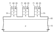
도 2는 본 발명의 바람직한 실시예에 따른 비휘발성 메모리 장치를 나타낸 평면도이다. 2 is a plan view illustrating a nonvolatile memory device according to an exemplary embodiment of the present invention.
도 2를 참조하면, 반도체 기판(10)상에 일방향(도 2에서 가로)으로 비트라인(BL)이 형성되고, 상기 비트라인(BL)과 수직인 방향(도 2에서 세로)으로 워드라인(WL)이 형성되어 있다. 상기 비트라인(BL)과 워드라인(WL)이 형성되는 가로/세로 방향은 상호간 바뀌어도 무방하다. 상기 비트라인(BL)의 하부의 소정 영역에는 반도체 기판(10)이 돌출된 필라(20)가 형성된다. 상기 필라(20)의 양측면에는 메모리층(30)과 워드라인(WL)이 형성된다. 여기서 특정 필라(20)의 양측면에 형성되는 한 쌍의 워드라인(WL)에 대해서, 상기 필라(20)가 형성되는 면을 내측면이라 칭하고 필라(20)가 형성되지 않는 면을 외측면이라 정의한다. 따라서 한 쌍의 워드라인(WL)의 내측면 중 상기 비트라인(WL)과 교차하는 영역에 필라(20)가 형성된다. 상기 워드라인(WL)과 메모리층(30)은 세로 방향으로 연결되어 형성되며, 세로 방향에 있어서 상기 필라(20)와 필라(20) 사이의 공간은 층간절연막(40)으로 채워져 있다. 또한 가로 방향에 있어서, 상기 필라(20)를 감싸는 한 쌍의 워드라인(WL)의 외측면에도 층간절연막(40)이 형성된다. 따라서 상기 필라(20)는 반도체 기판(10)상에 복수로 형성되지만 상호간에는 전기적으로 분리된다. 상기 메모리층(30)은 전하를 저장할 수 있는 전하저장막을 포함하며 단일의 필라에 대해 양 측면에 한 쌍의 메모리층(30)이 형성되므로, 필라(20) 하나가 저장할 수 있는 정보는 2비트가 된다. Referring to FIG. 2, a bit line BL is formed in one direction (horizontal in FIG. 2) on the
도 2에서, 상기 필라(20)의 좌우 폭을 F(최소가공크기를 의미; minimum Feature size)라 하고 상기 필라(20)와 필라(20) 사이의 가로/세로 간격 또한 F라 하면, 단일한 저장요소가 차지하는 면적은 2F2이 된다. 왜냐하면 상기 단일한 필라(20)가 차지하는 면적은 4F2이 되지만, 상기 필라(20)의 양측면에 2개의 전하저장막을 포함하는 메모리층(30)이 존재하므로 총 2비트가 저장될 수 있기 때문이다. 따라서 본 발명의 메모리 장치에 의하면, 1비트의 정보를 저장할 수 있는 공간이 도 1의 종래 메모리 장치에 비하여 절반으로 감소될 수 있어 고집적화에 기여할 수 있다. 여기서 상기 워드라인(WL)은, 통상의 모스 트랜지스터에 있어서 게이트 스페이서를 형성하는 방법을 적용하여 상기 필라(20)의 양 측면에 형성할 수 있다. 상기 필라(20)와 필라(20) 사이의 공간은 어차피 각 소자간 전기적 분리를 위한 층간절연막(40)으로 채워져야 하는데, 상기 공간을 활용하여 워드라인(WL)을 형성하므로 워드라인(WL)을 형성하기 위한 추가 공간이 필요하지는 않게 된다. In FIG. 2, when the left and right widths of the
이하 도면을 통하여 본 발명 메모리 장치의 수직 구조를 살펴보도록 하며, 편의상 n형의 트랜지스터를 전제로 설명한다. 도 3a는 도 2의 I-I'를, 도 3b는 도 2의 II-II'를, 도 3c는 도 2의 Ⅲ- Ⅲ'를, 도 3d는 도 2의 Ⅳ- Ⅳ'를, 도 3e는 도 2의 Ⅴ- Ⅴ'를 따라 취해진 단면도이다.Hereinafter, a vertical structure of the memory device of the present invention will be described with reference to the accompanying drawings. FIG. 3A shows I-I 'of FIG. 2, FIG. 3B shows II-II' of FIG. 2, FIG. 3C shows III-III 'of FIG. 2, FIG. 3D shows IV-IV' of FIG. Is a cross-sectional view taken along VV 'of FIG.
도 3a 및 도 3b는 비트라인 방향의 단면도로, 도 3a는 비트라인을 따라 절단한 면이고 도 3b는 비트라인과 비트라인 사이의 공간을 따라 절단한 면이다. 3A and 3B are cross-sectional views in the bit line direction. FIG. 3A is a plane cut along the bit line and FIG. 3B is a plane cut along the space between the bit line and the bit line.
도 3a를 참조하면, 반도체 기판(10)상에 상부로 돌출된 필라(20)가 형성되어 있고, 상기 필라(20)의 상부면에는 인접한 필라(20)를 연결하는 비트라인(BL)이 형성되어 있다. 상기 필라(20)의 양측면에는 메모리층(30)과 워드라인(WL)이 형성되며, 상기 필라(20)와 필라(20) 사이의 공간은 층간절연막(40)으로 채워진다. 상기 필라(20)의 하단부/상단부에는 불순물 이온이 주입된 소오스/드레인 영역(50,60)이 형성된다. 결국 단일의 필라(20)에 대해서, 상기 필라(20)의 소오스/드레인 영역(50,60)과 상기 필라(20)의 양측면에서 게이트 전극으로 작동하는 워드라인(WL)에 의하여, 한 쌍의 수직 채널 트랜지스터가 형성된다. 상기 수직 채널 트랜지스터가 n형이라면, p형의 기판상에 상기 n형 불순물 이온에 의한 소오스/드레인 영역(50,60)이 형성된다. 상기 소오스/드레인 영역(50,60)의 사이에는 채널 영역(55)이 형성된다. 여기서 상기 소오스 영역(50)은, 도 3a에 도시된 바와 같이, 상기 필라 (20)의 하단부 및 상기 반도체 기판(10)의 표면을 따라 전체적으로 연결되게 형성될 수 있다. 이 경우 상기 소오스 영역(50)을 전기적으로 연결하기 위해 필요한 콘택을 형성하기 위한 공간을 줄일 수 있다. Referring to FIG. 3A, a
본 발명의 메모리 장치를 부유 트랩형에 적용한다면, 상기 메모리층(30)은 터널 절연막/전하저장막/블로킹 절연막을 포함한다. 상기 터널 절연막은 통상 실리콘 반도체 기판을 산화시킨 열산화막(SiO2)으로 이루어진다. 상기 전하저장막은, 트랩 밀도가 높고 전자친화력이 터널 절연막이나 블로킹 절연막에 비하여 높은 절연막으로 통상 실리콘질화막(Si3N4)을 사용하며, 기타 실리콘 옥시나이트라이드막(SiON), 강유전체막(ferroelectric layer) 등이 사용될 수 있다. 마지막으로 상기 블로킹 절연막으로는, 통상 실리콘 산화막이 사용되나, 높은 유전 상수를 가지며 에너지 밴드갭이 큰 산화 알루미늄막(Al2O3)과 같은 금속산화막 등이 사용될 수 있다. 위와 같이 구성된 메모리층(30)은 상기 필라(20)의 양측면을 모두 덮도록 형성된다. 상기 메모리층(30)의 외측면에는 게이트 전극에 해당하는 워드라인(WL)이 형성된다. 상기 워드라인(WL)은 폴리실리콘이나 또는 저항을 낮추기 위한 금속/금속 실리사이드를 조합하여 사용할 수 있다. 상기 워드라인(WL)은 채널 영역(55)에 중첩되도록 형성되며, 상기 워드라인(WL)의 양 끝단은 소오스/드레인 영역(50,60)과 일부 중첩된다. 상기 워드라인(WL)의 하부면과 상기 필라(20)의 하단부에 인접한 반도체 기판(10)의 상부면 사이는 일정한 갭이 존재한다. 상기 갭은 인접한 필라(20)와 필라(20) 사이를 절연시키는 층간절연막(40)으로 채워진다. 또는 제조 공정 상 상기 메모리층(30)이 반도체 기판(10)의 상부면을 덮도록 연장되어, 상기 메모리층(30)이 상기 워드라인(WL)의 하부면과 반도체 기판(10)의 상부면 사이의 갭에 형성될 수 있다. When the memory device of the present invention is applied to the floating trap type, the
상기 개개의 필라(20)는 2비트를 저장하는 단위 저장요소에 해당하므로, 필라(20)와 필라(20) 사이의 공간은 전기적으로 절연된다. 이를 위해, 도 2에 도시된 바와 같이, 필라(20)와 필라(20) 사이는 가로방향으로나 세로방향으로 모두 층간절연막(40)이 형성된다. 상기 가로방향/세로방향의 층간절연막(40)은 제조 공정상 형성되는 시점이 차이날 수는 있지만, 실질적으로 동일한 기능을 가진 막이므로 동일한 도면부호를 사용한다. 한편, 도 3b의 비트라인(BL) 사이의 공간을 절단한 면에서, 메모리층(30)과 워드라인(WL)은 중단없이 연속적으로 형성되어 있는데 비해 필라(20)는 층간절연막(40)에 의해 분리되어 있음을 확인할 수 있다. Since the
도 3c 및 도 3e는 워드라인 방향의 단면도로, 도 3c는 필라이 형성된 라인을 따라 절단한 면이고 도 3d는 워드라인과 워드라인 사이의 공간을 따라 절단한 면이며 도 3e는 워드라인을 따라 절단한 면이다. 3C and 3E are cross-sectional views in the word line direction, FIG. 3C is a plane cut along the line formed with a pillar, FIG. 3D is a plane cut along the space between the word line and the word line, and FIG. 3E is cut along the word line. One side.
도 3c를 참조하면, 반도체 기판(10)상에 상측으로 돌출된 필라(20)가 형성되며 상기 필라(20)의 상부로 비트라인(BL)이 형성되어 있다. 상기 필라(20)와 필라(20) 사이는 층간절연막(40)이 형성되며, 상기 필라(20)는 소오스/드레인 영역(50,60)과 그 사이에 형성되는 채널 영역(55)으로 구분된다. Referring to FIG. 3C, a
도 3d를 참조하면, p형의 반도체 기판(10)상에 소오스 영역(50)의 일부를 구성하는 n형의 불순물 이온층이 형성되어 있다. 도 3d는 워드라인 사이의 공간을 절 단한 면이므로, 상기 n형의 불순물 이온층의 상부에는 층간절연막(40)과 비트라인(BL)만이 형성된다. 도 3e를 참조하면, 반도체 기판(10)의 표면에 층간절연막(40)을 개재하여 워드라인(WL)이 형성되어 있다. 상기 반도체 기판(10)과 워드라인(WL) 사이의 절연막은 층간절연막(40)외에 메모리층(30)으로 형성할 수 있다. 상기 메모리층(30)으로 형성하는 기술은 본 발명의 제조 공정을 살펴보면서 설명하도록 한다. Referring to FIG. 3D, an n-type impurity ion layer constituting a part of the
위와 같은 구조로 된 본 발명의 비휘발성 메모리 장치의 동작 과정을 살펴 본다. 도 2 및 도 3a를 재차 참조하면, 특정한 비트라인(BL)과 워드라인(WL)이 선택되면 그에 따라 단일의 필라(20)가 정해진다. 이 때 상기 필라(20)의 양측면에 존재하는 워드라인(WL) 중 하나의 워드라인(WL)에 의해 필라(20)의 좌우측면 중 한쪽 면이 결정된다. 이와 같이 필라(20)의 특정면을 선택한 후, 상기 필라의 선택면상의 메모리층(30)에 전하를 주입하거나 저장된 전하를 방출함으로써 프로그램 또는 소거 동작이 이루어지게 된다. An operation process of the nonvolatile memory device of the present invention having the above structure will be described. Referring again to FIGS. 2 and 3A, when a specific bit line BL and word line WL are selected, a
상기 필라(20), 메모리층(터널링 절연막/전하저장막/블로킹 절연막)(30), 워드라인(WL)에 해당하는 물질들은 각각 고유의 에너지 밴드 갭을 가지고 있어, 에너지 밴드 갭의 차이에 의해 각각의 계면에 전위장벽(potential barrier)을 형성한다. 전하를 주입하는 경우 통상의 채널 핫전자 주입(Channel hot electron injection) 방식 또는 파울러-노더하임(Fowler-Nordheim, FN) 터널링 방식이 모두 가능하다. 가령 상기 워드라인(WL) 및 드레인 영역(60)에 양전압을 인가하고 소오스 영역(50)을 접지시키면, 소오스 영역(50)의 전자들이 드레인 영역(60)으로 가속 되는데, 이 중 일부가 터널링 절연막의 전위장벽을 통과하여 전하저장막에 포획되도록 할 수 있다. 이와 같이 전하저장막내에 전자가 포획되어 축적되면 수직 채널 트랜지스터의 문턱전압(threshold voltage)이 상승하여 프로그램 상태(또는 소거 상태)가 된다. 반대로 상기 워드라인(WL)에 음전압을 인가하는 등의 방법으로 채널 영역(55)에서 워드라인(WL)으로 전계가 형성되도록 하면, 상기 전하저장막 내에 포획되어 있던 전자가 터널링 절연막을 통하여 반도체 기판(10)으로 방출된다. 이 때 상기 트랜지스터의 문턱전압이 낮아져 소거상태(또는 프로그램 상태)가 된다. 따라서 데이터를 판독하는 경우에는 상기 트랜지스터의 문턱전압의 크기에 따라 전하저장막 내에 전자가 포획되었는지 여부를 판단한다. The materials corresponding to the
도 4a 내지 도 4e는 본 발명의 다른 실시예에 의한 것으로, 도 4a는 도 2의 I-I'를, 도 4b는 도 2의 II-II'를, 도 4c는 도 2의 Ⅲ- Ⅲ'를, 도 4d는 도 2의 Ⅳ- Ⅳ'를, 도 4e는 도 2의 Ⅴ- Ⅴ'를 따라 취해진 단면도이다.Figures 4a to 4e according to another embodiment of the present invention, Figure 4a is I-I 'of Figure 2, Figure 4b is II-II' of Figure 2, Figure 4c is III-III 'of Figure 2 4D is a cross-sectional view taken along line IV-IV 'of FIG. 2, and FIG. 4E is taken along line V-V' of FIG.
도 4a를 참조하면, 반도체 기판(10)상에 상부로 돌출된 필라(20)가 형성되고, 상기 필라(20)의 상부면에는 비트라인(BL)이 형성된다. 상기 필라(20)의 양측면에는 메모리층(30)과 워드라인(WL)이 형성되며, 상기 필라(20)와 필라(20) 사이의 공간은 층간절연막(40)으로 채워진다. 상기 필라(20)의 하단부/상단부에는 불순물 이온이 주입된 소오스/드레인 영역(50,60)이 형성되며, 상기 소오스/드레인 영역(50,60)과 상기 워드라인(WL)은 수직 트랜지스터를 형성한다. 구체적으로, 상기 소오스 영역(50)은 상기 필라(20)의 하단부 일부와 인접한 두 개의 필라(20)의 좌 측면과 우측면 사이의 반도체 기판(10)에 형성되며, 상기 수직 트랜지스터의 채널 영역(55)과 반도체 기판(10)은 서로 연결된다. 즉, 도 3a의 구조와 달리, 상기 채널영역(55)과 반도체 기판(10)이 소오스 영역(50)에 의해 분리되지 않고 전기적으로 도통된다. 따라서 메모리층(30)에 포함된 전하저장막에 전하를 주입하거나 방출하는 경우, 반도체 기판(10)을 통해 채널 영역(55)에 양전압 또는 음전압을 직접 인가할 수 있어 다양한 제어 방식을 확보할 수 있는 장점이 있다. 또한 채널 영역(55)과 반도체 기판(10)이 상호 연결된 경우 소위 플로팅 바디 효과를 방지할 수 있다. Referring to FIG. 4A, a
일반적으로 플로팅 바디 효과란, 트랜지스터가 동작시 발생하는 열이나 또는 고에너지의 열전자(hot carrier)가 실리콘 원자와 충돌하여 발생하는 전자-정공 쌍이 축적되는 현상을 의미한다. 플로팅 바디 효과에 의해, 열이나 전자-정공 쌍이 축적되면 문턱 전압등과 같은 소자 특성에 변동이 생기고 동작상에 신뢰성이 떨어지는 문제점이 있다. 그런데, 도 4a와 같이 소오스 영역(50)이 분리되어 형성되면, 채널 영역(55)이 하부의 p형 반도체 기판(10)과 연결되어 전자-정공 쌍의 배출 통로가 형성되므로 플로팅 바디 효과를 방지할 수 있게 된다. In general, the floating body effect refers to a phenomenon in which an electron-hole pair generated by a heat generated when the transistor is operated or a hot energy of a hot carrier collides with a silicon atom. Due to the floating body effect, when a heat or an electron-hole pair is accumulated, device characteristics such as a threshold voltage may be changed and reliability may be deteriorated in operation. However, when the
도 4b는 비트라인(BL) 사이의 공간을 절단한 단면으로 이를 참조하면, 메모리층(30)과 워드라인(WL)은 중단없이 연속적으로 형성되어 있다. 이에 비하여 도 4a에서 상기 메모리층(30) 사이에 형성되었던 필라(20)는 층간절연막(40)으로 대체된다. 따라서 상기 층간절연막(40)에 의해 개개의 필라(20)들은 전기적으로 절연되며, 각 필라(20)는 2비트를 저장하는 단위 저장요소로 사용된다. 4B is a cross-sectional view of the space between the bit lines BL. Referring to this, the
한편, 상기 소오스 영역(50)은 반도체 기판(10)의 표면을 따라 단일한 영역으로 형성되어 있다. 즉, 상기 소오스 영역(50)은 필라(20)의 하부에서는 일정한 영역으로 분리되고, 필라(20)가 형성되지 않은 층간절연막(40)의 하부에서는 연결된 구조로 이루어진다. 상기 반도체 기판(10)의 상부면에 필라(20)가 형성되어 있지 않으므로, 상기 단일하게 된 소오스 영역(50)은 반도체 기판(10)과 채널 영역(55)을 차단하는 것은 아니다. 또한 소오스 영역(50)이 전체적으로 연결되므로 소오스 영역(50)의 콘택 공간을 줄일 수 있다. Meanwhile, the
도 4c는 워드라인(WL) 방향의 단면도로 필라(20)가 형성된 라인의 중앙을 절단한 것이다. 도 4c에 도시된 바와 같이, 소오스 영역(50)은 전체적으로 연결되도록, 불순물 이온이 주입되는 소오스 영역(50)이 필라(20) 사이의 층간절연막(40) 하부에 형성된다. 마찬가지로, 도 4d의 워드라인(WL)과 워드라인(WL) 사이의 층간절연막(40) 중심부를 따라 절단한 단면을 참조하면, 반도체 기판(10)상에 전체적으로 연결되어 있는 소오스 영역(50)의 일부가 불순물 이온층으로서 형성되어 있다. 한편, 도 4e와 같이 워드라인을 따라 절단한 면에서는, 반도체 기판(10)에 소오스 영역(50)이 형성되고, 그 상부로 층간절연막(40)/워드라인(WL)/층간절연막(40)이 형성되어 있다. 위와 같은 구조에 의한 비휘발성 메모리 장치는, 다양한 제어 방식을 확보하고 플로팅 바디 효과를 방지한다는 점을 제외하면, 도 3a 내지 도 3e에 도시된 메모리 장치와 동일하게 동작한다. 4C is a cross-sectional view of the
이상으로 본 발명의 메모리 장치에 대해 부유 트랩형인 경우를 예로서 살펴 보았다. 그러나 본 발명은 수직 방향 채널이 형성되도록 워드라인이 반도체 기판이 돌출된 양 측면으로 형성된 점에 착안한 것이므로, 다양한 메모리 장치에 대해서도 적용될 수 있다. 가령 도 2 및 도 3a 내지 도 3e/도 4a 내지 도 4e의 예시도면에서 메모리층이 절연막으로 고립된 부유 게이트를 포함하도록 하면 부유 게이트형 비휘발성 메모리 장치에 대해서도 적용될 수 있을 것이다. In the above, the case of the floating trap type | mold with respect to the memory device of this invention was examined as an example. However, the present invention focuses on the fact that the word line is formed on both sides of the protruding semiconductor substrate so that the vertical channel is formed, and thus may be applied to various memory devices. For example, in the exemplary drawings of FIGS. 2 and 3A to 3E / 4A to 4E, if the memory layer includes a floating gate isolated with an insulating layer, the floating gate type nonvolatile memory device may be applied.
이하에서는 도 2 및 도 3a 내지 도 3e에 도시된 비휘발성 메모리 장치를 제조하기 위한 제조과정을 살펴본다. 다만 하기의 제조 과정은 본 발명의 메모리 장치를 제조하기 위한 다양한 방법 중 하나이며, 본 발명의 장치가 반드시 하기의 방법으로만 제조될 수 있는 것은 아니다. 상기한 제조 방법은 도 3a 내지 도 3e에 도시된 메모리 장치를 중심으로 설명할 것이며, 이는 도 4a 내지 도 4e에 도시된 장치에 대해서도 거의 동일하게 적용된다. 다만 일부 차이나는 점에 대해서는 해당 부분에서 언급하도록 한다. Hereinafter, a manufacturing process for manufacturing the nonvolatile memory device illustrated in FIGS. 2 and 3A to 3E will be described. However, the following manufacturing process is one of various methods for manufacturing the memory device of the present invention, and the device of the present invention may not necessarily be manufactured only by the following method. The above manufacturing method will be described with reference to the memory device shown in Figs. 3A to 3E, and the same applies to the device shown in Figs. 4A to 4E. However, some differences are mentioned in the relevant section.
도 5a 내지 도 10a는 본 발명의 실시예에 따른 공정단면도로 도 2의 I-I'를 따라 취해진 것이며, 도 5b 내지 도 10b는 본 발명의 실시예에 따른 공정단면도로 도 2의 Ⅲ-Ⅲ'를 따라 취해진 것이다. 5A to 10A are taken along the line II ′ of FIG. 2 according to an embodiment of the present invention, and FIGS. 5B to 10B are III-III of FIG. 2 according to an embodiment of the present invention. Was taken along.
도 5a 및 도 5b를 참조하면, p형의 반도체 기판(10)상에 불순물 이온을 주입하여, 반도체 기판(10)의 표면 및 반도체 기판(10)의 표면으로부터 소정 깊이에 불순물 이온층(50a,60a)을 형성한다. 상기 불순물 이온층(50a,60a)은 후속 공정에서 소오스/드레인 영역이 된다. 상기 불순물 이온층(50a,60a)은 각각 상이한 에너지를 가하여 반도체 기판(10)으로부터 다른 깊이에 형성되도록 한다. 또는 p형 반도체 기판상에 이온 주입 또는 확산을 통하여 n형 불순물 이온층(50a)을 형성한 후, 상기 불순물 이온층(50a)상에 p형 실리콘막(55a)을 성장시키고 상기 p형 실리콘 막(55a) 표면에 n형 불순물 이온층(60a)을 형성할 수 있다. 만약 도 4a 내지 도 4e와 같이 반도체 기판과 채널 영역이 연결된 장치를 제조하는 경우에는, 미리 불순물 이온층(50a,60a)을 형성하는 대신 공정 중에 불순물 이온을 주입할 수 있다. 5A and 5B, impurity ions are implanted onto a p-
도 6a 및 도 6b를 참조하면, 상기 불순물 이온층(50a,60a)이 형성된 반도체 기판(10)상에 마스크(70)를 형성하여 소정 영역을 식각한다. 상기 마스크(70)는 실리콘질화막 성분의 통상의 질화막마스크(70)를 이용한다. 이를 위해, 먼저 반도체 기판(10)상에 실리콘질화막(Si3N4)를 증착한 후, 포토레지스트를 이용한 사진 식각 공정으로 상기 실리콘질화막의 일부를 식각하여 마스크(70)를 형성한다. 상기 마스크(70)는 도 2에서 세로방향으로 필라(20)을 덮도록 형성되는 것이다. 이어서 상기 마스크(70)에 의해 노출된 반도체 기판(10)을 식각하여 핀(20a)를 형성한다. 이 때 반도체 기판(10)의 식각되는 깊이를 적절히 조절하여, 도 6a와 같이, 상기 n형 불순물 이온층(50a)의 일부는 핀(20a)의 하단부에 속하고 일부는 반도체 기판(10)의 표면을 따라 전체적으로 연결되도록 한다. 6A and 6B, a
도 7a 및 도 7b를 참조하면, 상기 핀(20a)의 좌우측면에 메모리층(30)과 워드라인(WL)을 형성한다. 상기 메모리층(30)은, 터널 절연막/전하저장막/블로킹 절연막을 포함한다. 통상 상기 터널 절연막이나 블로킹 절연막은 실리콘 산화막(SiO2)을 사용하며 상기 전하저장막은 실리콘질화막(Si3N4)을 이용한다. 상기한 막들은 열 산화 또는 화학기상증착(CVD; Chemical Vapor Deposition) 방법으로 형성한다. 막이 형성된 후에는, 반도체 기판(10)을 따라 형성된 메모리층(30)을 제외하고 마스크(70)의 상부에 증착된 막들은 화학기계적연마(CMP; Chemical Mechanical Polishing)등을 이용하여 제거한다. Referring to FIGS. 7A and 7B, the
도 7a에 도시된 바와 같이, 핀(20a)의 양측면외에 반도체 기판(10)의 표면에도 메모리층(30)이 형성되어 있다. 그런데 전하가 이동하는 채널은 상기 핀(20a)의 측면에만 형성되므로, 상기 반도체 기판(10)의 표면에 형성된 메모리층(30)은 전하를 저장하는 동작과는 관계가 없으며 불필요하다. 따라서 상기 반도체 기판(10)의 표면에 형성된 메모리층(30)만 별도로 제거한 후, 제거된 영역을 후속 공정에서 층간절연막으로 채워도 무방하다. 하지만 상기 메모리층(30) 또한 절연체로 이루어져 있어 절연막으로서 역할을 수행할 수 있으므로, 상기 반도체 기판(10)의 표면에 형성된 메모리층(30)을 제거하는 별도의 공정을 추가함이 없이, 이를 그대로 남겨두는 것이 효율적이다. As shown in FIG. 7A, the
이어서 워드라인(WL)을 형성한다. 상기 워드라인(WL)은, 통상의 모스 트랜지스터에서 게이트 스페이서를 형성하기 위한 공정을 적용하여, 도전막을 반도체 기판(10)상에 증착한 후 에치백을 진행하여 형성한다. 위와 같이 워드라인(WL)이 형성된 후에 소오스/드레인 영역을 위한 불순물 이온을 주입할 수 있다. 특히 도 4a와 같이 채널 영역(55)과 반도체 기판(10)이 연결된 구조에서는, 초기에 불순물 이온층(50a,60a)이 형성된 반도체 기판(10)을 준비할 수도 있지만 워드라인(WL)을 형성한 후 불순물 이온을 주입하는 방법을 사용할 수 있다. Subsequently, a word line WL is formed. The word line WL is formed by depositing a conductive film on the
도 4a와 같이 채널 영역(55)과 반도체 기판(10)이 연결되려면, 상기 핀(20a) 하부 영역의 반도체 기판(10)에는 불순물 이온이 주입되지 않고 소오스 영역이 형성되지 않는다. 만약 초기 상태에서 특정 영역에만 불순물 이온이 주입되도록 하려면 별도의 마스크를 사용해야 한다. 그런데, 워드라인(WL) 형성 후에는 별도의 마스크 없이 상기 워드라인(WL)을 기준으로 핀(20a)과 핀(20a)의 사이의 필요한 영역으로 불순물 이온을 주입할 수 있다. 위와 같이 불순물 이온이 주입된 후에는 통상 이온 주입 단계에서의 손상을 치유하기 위한 어닐링(annealing)이 진행되며, 이로 인하여 상기 불순물 이온은 핀(20a) 하단부의 가장자리까지 확산된다. 이 때, 상기 핀(20a) 하부와 인접한 반도체 기판(10)에는 상기 핀을(20a)을 덮고 있는 마스크(70)에 의해 불순물 이온 주입이 차단되어, 불순물 이온층(50a)은 전체적으로 연결되지 못하고 상호 분리되어 있다. 만약 콘택 영역을 줄일 수 있도록 상기 분리된 불순물 이온층(50a)을 연결하려면, 후속 공정에서 추가적인 불순물 이온 주입 단계가 필요하다. 한편 드레인 영역에 있어서는, 도 3a 또는 도 4a의 장치에서 동일한 구조이며 동일하게 형성된다. As shown in FIG. 4A, when the
도 8a 및 8b를 참조하면, 상기 핀(20a) 사이의 공간에 층간절연막(40)을 형성한다. 즉, 상기 핀(20a)사이의 공간을, USG(Undoped Silicate Glass)막, HDP(High Density Plasma) 산화막, PECVD(Plasma Enhanced Chemical Vapor Deposition) 법을 이용한 TEOS(Tatra Ethyl Otho Silicate)막과 같은 절연막으로 매립한다. 이어서 상기 절연막을 앞서 핀(20a)를 형성하기 위해 사용하였던 마스크(70)의 상부 표면과 동일한 레벨까지 평탄화한다. 여기서 평탄화 과정은 화학기계 적연마 등을 사용할 수 있다. 8A and 8B, an
도 9a 및 도 9b를 참조하면, 상기 핀(20a)의 소정 영역을 식각하여 필라(20)를 형성한다. 이를 위해, 먼저 상기 필라(20)가 형성될 영역을 정의하는 실리콘질화막 성분의 마스크(71)를 형성한 후, 상기 핀(20a)에서 마스크(71)로 노출된 영역을 건식 식각으로 제거한다. 9A and 9B, a
상기 마스크(71)는 핀(20a) 중 필라(20)가 형성될 영역을 덮는 것으로, 상기 핀(20a) 형성을 위해 사용하였던 마스크(70)를 이용함이 바람직하다. 즉, 상기 핀(20a)이 형성될 영역을 덮도록 형성되는 마스크(70)의 소정 영역을 사진 식각으로 제거하여 상기 핀(20a) 중 필라(20)가 형성될 영역을 덮는 마스크(71)를 형성한다. 이어서 상기 마스크(71)에 따라 노출된 핀(20a)의 영역을 식각하면 복수의 필라(20)가 형성되며, 상기 필라(20)가 형성되면서 불순물 이온층(50a,60a)으로부터 소오스 영역(50)/드레인 영역(60)이 형성된다. The
앞서 살펴 본 바와 같이, 도 4a의 구조를 위해 워드라인(WL)을 형성한 후 불순물 이온을 주입한 경우, 상기 불순물 이온층(50a)을 전체적으로 연결하기 위한 추가적인 불순물 이온 주입 단계가 필요하다. 그런데 본 단계에서 상기 마스크(71)에 의해 필라(20) 사이의 영역이 노출되므로, 상기 노출 영역으로 불순물 이온을 주입하면 종래 핀(20a)의 하부에서 분리되어 있었던 불순물 이온층(50a)이 연결되면서 공통 소오스 영역(50a)이 형성된다. As described above, when impurity ions are implanted after forming the word line WL for the structure of FIG. 4A, an additional impurity ion implantation step for connecting the
도 10a 및 도 10b를 참조하면, 상기 핀(20a)의 식각된 부분에 층간절연막(40)을 형성한다. 이는 앞서 핀(20a) 사이의 공간을 채웠던 층간절연막(40)과 동일 하게 형성한다. 즉, 상기 필라(20)을 형성하면서 핀(20a)에서 식각된 부분을 HDP(High Density Plasma) 산화막 등으로 채운 후 화학기계적 연마에 의한 평탄화를 진행한다. 이 후 상기 질화막 마스크(71)는 인산 스트립 등의 방법으로 제거하고, 상기한 결과물상에 비트라인용 도전성 물질을 증착한 후 이를 패터닝하여 비트라인을 형성하면, 도 3a 내지 도 3e의 메모리 장치가 완성된다. 10A and 10B, an
이 때 상기 마스크(71)를 제거한 상태에서 상기 필라(20)의 상부면이 외부로 노출되어 있음을 이용하여, 불순물 이온을 주입하여 드레인 영역(60)을 형성할 수 있다. 물론, 앞서 살펴 본 바와 같이, 상기 드레인 영역(60)은 초기의 불순물 이온층(60a)으로부터 형성할 수도 있다. 한편, 상기 마스크(71)가 제거된 영역으로 비트라인(BL)용 도전성 물질이 채워지므로, 비트라인(BL)과 필라(20)간 콘택은 자동적으로 자기정렬(self-align) 방식에 의해 형성된다. In this case, the
이상에서 살펴 본 바와 같이 본 발명의 비휘발성 반도체 메모리 장치 및 그 제조방법에 의하면, 종래와 동일한 크기에서 2배의 데이터 저장 능력을 보유하여 고집적화에 유리한 효과가 있다. 또한 본 발명의 실시예에서, 반도체 기판과 채널 영역이 연결되도록 하면 다양한 방식으로 메모리를 제어할 수 있고 또한 동작시 플로팅 바디 효과를 방지할 수 있다.As described above, according to the nonvolatile semiconductor memory device and the manufacturing method thereof of the present invention, it has a double data storage capacity at the same size as in the prior art and has an advantageous effect on high integration. In addition, in the embodiment of the present invention, when the semiconductor substrate and the channel region are connected, the memory can be controlled in various ways and the floating body effect can be prevented during operation.
Claims (13)
Priority Applications (5)
| Application Number | Priority Date | Filing Date | Title |
|---|---|---|---|
| KR1020050086443A KR100697291B1 (en) | 2005-09-15 | 2005-09-15 | Nonvolatile Semiconductor Memory Device and Manufacturing Method Thereof |
| US11/520,886 US7525146B2 (en) | 2005-09-15 | 2006-09-14 | Nonvolatile semiconductor memory devices |
| CNA2006101537461A CN1933163A (en) | 2005-09-15 | 2006-09-15 | Nonvolatile semiconductor memory devices and methods of forming the same |
| US12/410,010 US7906397B2 (en) | 2005-09-15 | 2009-03-24 | Methods of fabricating nonvolatile semiconductor memory devices including a plurality of stripes having impurity layers therein |
| US13/047,403 US8575672B2 (en) | 2005-09-15 | 2011-03-14 | Nonvolatile semiconductor memory devices |
Applications Claiming Priority (1)
| Application Number | Priority Date | Filing Date | Title |
|---|---|---|---|
| KR1020050086443A KR100697291B1 (en) | 2005-09-15 | 2005-09-15 | Nonvolatile Semiconductor Memory Device and Manufacturing Method Thereof |
Publications (1)
| Publication Number | Publication Date |
|---|---|
| KR100697291B1 true KR100697291B1 (en) | 2007-03-20 |
Family
ID=37854218
Family Applications (1)
| Application Number | Title | Priority Date | Filing Date |
|---|---|---|---|
| KR1020050086443A Expired - Fee Related KR100697291B1 (en) | 2005-09-15 | 2005-09-15 | Nonvolatile Semiconductor Memory Device and Manufacturing Method Thereof |
Country Status (3)
| Country | Link |
|---|---|
| US (3) | US7525146B2 (en) |
| KR (1) | KR100697291B1 (en) |
| CN (1) | CN1933163A (en) |
Cited By (4)
| Publication number | Priority date | Publication date | Assignee | Title |
|---|---|---|---|---|
| US7646041B2 (en) | 2006-12-04 | 2010-01-12 | Samsung Electronics Co., Ltd. | Non-volatile memory devices including vertical channels, methods of operating, and methods of fabricating the same |
| US7928501B2 (en) | 2008-07-04 | 2011-04-19 | Samsung Electronics Co., Ltd. | Semiconductor device and methods of forming and operating the same |
| KR101056060B1 (en) * | 2008-11-11 | 2011-08-11 | 한국과학기술원 | Self-aligned contact formation method of vertical transistor and vertical transistor including contact hole |
| KR20230049237A (en) * | 2021-10-06 | 2023-04-13 | 서울시립대학교 산학협력단 | Short-term flash memory device and array |
Families Citing this family (29)
| Publication number | Priority date | Publication date | Assignee | Title |
|---|---|---|---|---|
| KR100697291B1 (en) * | 2005-09-15 | 2007-03-20 | 삼성전자주식회사 | Nonvolatile Semiconductor Memory Device and Manufacturing Method Thereof |
| KR100881392B1 (en) * | 2006-10-31 | 2009-02-05 | 주식회사 하이닉스반도체 | Semiconductor device with vertical transistor and manufacturing method thereof |
| JP2008192804A (en) * | 2007-02-05 | 2008-08-21 | Spansion Llc | Semiconductor device and manufacturing method thereof |
| KR100866966B1 (en) * | 2007-05-10 | 2008-11-06 | 삼성전자주식회사 | Nonvolatile Memory Devices, Manufacturing Methods And Semiconductor Packages |
| US20090179253A1 (en) | 2007-05-25 | 2009-07-16 | Cypress Semiconductor Corporation | Oxide-nitride-oxide stack having multiple oxynitride layers |
| US8614124B2 (en) | 2007-05-25 | 2013-12-24 | Cypress Semiconductor Corporation | SONOS ONO stack scaling |
| US9299568B2 (en) | 2007-05-25 | 2016-03-29 | Cypress Semiconductor Corporation | SONOS ONO stack scaling |
| US9449831B2 (en) | 2007-05-25 | 2016-09-20 | Cypress Semiconductor Corporation | Oxide-nitride-oxide stack having multiple oxynitride layers |
| US8063434B1 (en) | 2007-05-25 | 2011-11-22 | Cypress Semiconductor Corporation | Memory transistor with multiple charge storing layers and a high work function gate electrode |
| US8940645B2 (en) | 2007-05-25 | 2015-01-27 | Cypress Semiconductor Corporation | Radical oxidation process for fabricating a nonvolatile charge trap memory device |
| US8633537B2 (en) | 2007-05-25 | 2014-01-21 | Cypress Semiconductor Corporation | Memory transistor with multiple charge storing layers and a high work function gate electrode |
| JP2008305832A (en) * | 2007-06-05 | 2008-12-18 | Panasonic Corp | Nonvolatile semiconductor memory device and manufacturing method thereof |
| KR100908819B1 (en) * | 2007-11-02 | 2009-07-21 | 주식회사 하이닉스반도체 | Semiconductor device with vertical channel transistor and manufacturing method thereof |
| US9431549B2 (en) | 2007-12-12 | 2016-08-30 | Cypress Semiconductor Corporation | Nonvolatile charge trap memory device having a high dielectric constant blocking region |
| KR20090126077A (en) * | 2008-06-03 | 2009-12-08 | 삼성전자주식회사 | Memory semiconductor device and manufacturing method thereof |
| KR101723864B1 (en) * | 2010-10-08 | 2017-04-07 | 삼성전자주식회사 | Semiconductor Device With Vertical Channel Transistor And Method Of Fabricating The Same |
| US8530312B2 (en) | 2011-08-08 | 2013-09-10 | Micron Technology, Inc. | Vertical devices and methods of forming |
| WO2014008160A2 (en) * | 2012-07-01 | 2014-01-09 | Cypress Semiconductor Corporation | Sonos ono stack scaling |
| US9112047B2 (en) * | 2013-02-28 | 2015-08-18 | Freescale Semiconductor, Inc. | Split gate non-volatile memory (NVM) cell and method therefor |
| US9276108B2 (en) * | 2014-06-26 | 2016-03-01 | Taiwan Semiconductor Manufacturing Company Limited | Memory cell array and cell structure thereof |
| US10002876B2 (en) * | 2014-10-29 | 2018-06-19 | International Business Machines Corporation | FinFET vertical flash memory |
| US9748389B1 (en) | 2016-03-25 | 2017-08-29 | Taiwan Semiconductor Manufacturing Co., Ltd. | Method for semiconductor device fabrication with improved source drain epitaxy |
| US9935101B2 (en) * | 2016-07-27 | 2018-04-03 | International Business Machines Corporation | Vertical field effect transistor with uniform gate length |
| KR102699046B1 (en) * | 2016-12-15 | 2024-08-27 | 삼성전자주식회사 | Integrated circuit having vertical transistor and semiconductor device including the same |
| US12058867B2 (en) | 2020-06-18 | 2024-08-06 | Taiwan Semiconductor Manufacturing Company, Ltd. | Memory device |
| US11985808B2 (en) | 2021-07-05 | 2024-05-14 | Changxin Memory Technologies, Inc. | Memory and method for manufacturing same |
| US12108588B2 (en) | 2021-07-05 | 2024-10-01 | Changxin Memory Technologies, Inc. | Memory and method for manufacturing same |
| CN113594163B (en) * | 2021-07-05 | 2023-12-19 | 长鑫存储技术有限公司 | Memory and manufacturing method thereof |
| CN115589716A (en) * | 2021-07-05 | 2023-01-10 | 长鑫存储技术有限公司 | Memory and manufacturing method thereof |
Citations (4)
| Publication number | Priority date | Publication date | Assignee | Title |
|---|---|---|---|---|
| KR19980069975A (en) * | 1997-01-22 | 1998-10-26 | 포만제프리엘 | Semiconductor device and method of forming the same |
| JP2002083945A (en) | 2000-09-08 | 2002-03-22 | Toshiba Corp | Semiconductor memory device and method of manufacturing the same |
| US20040232471A1 (en) | 2001-09-20 | 2004-11-25 | Shoji Shukuri | Semiconductor integrated circuit device and its manufacturing method |
| KR20050010963A (en) * | 2002-06-21 | 2005-01-28 | 마이크론 테크놀로지, 인크. | Vertical nrom |
Family Cites Families (32)
| Publication number | Priority date | Publication date | Assignee | Title |
|---|---|---|---|---|
| US4737829A (en) * | 1985-03-28 | 1988-04-12 | Nec Corporation | Dynamic random access memory device having a plurality of one-transistor type memory cells |
| US5432739A (en) * | 1994-06-17 | 1995-07-11 | Philips Electronics North America Corporation | Non-volatile sidewall memory cell method of fabricating same |
| US5874760A (en) * | 1997-01-22 | 1999-02-23 | International Business Machines Corporation | 4F-square memory cell having vertical floating-gate transistors with self-aligned shallow trench isolation |
| US5990509A (en) * | 1997-01-22 | 1999-11-23 | International Business Machines Corporation | 2F-square memory cell for gigabit memory applications |
| US6337497B1 (en) * | 1997-05-16 | 2002-01-08 | International Business Machines Corporation | Common source transistor capacitor stack |
| US5973356A (en) * | 1997-07-08 | 1999-10-26 | Micron Technology, Inc. | Ultra high density flash memory |
| US5936274A (en) * | 1997-07-08 | 1999-08-10 | Micron Technology, Inc. | High density flash memory |
| US6150687A (en) | 1997-07-08 | 2000-11-21 | Micron Technology, Inc. | Memory cell having a vertical transistor with buried source/drain and dual gates |
| DE19811882A1 (en) * | 1998-03-18 | 1999-09-23 | Siemens Ag | DRAM cell arrangement |
| US6026019A (en) * | 1998-06-19 | 2000-02-15 | International Business Machines Corporation | Two square NVRAM cell |
| US6134175A (en) * | 1998-08-04 | 2000-10-17 | Micron Technology, Inc. | Memory address decode array with vertical transistors |
| US5977579A (en) * | 1998-12-03 | 1999-11-02 | Micron Technology, Inc. | Trench dram cell with vertical device and buried word lines |
| DE19933564C1 (en) * | 1999-07-16 | 2001-01-25 | Infineon Technologies Ag | Method for producing a vertical semiconductor transistor component and vertical semiconductor transistor component |
| EP2988331B1 (en) * | 2000-08-14 | 2019-01-09 | SanDisk Technologies LLC | Semiconductor memory device |
| US6580124B1 (en) * | 2000-08-14 | 2003-06-17 | Matrix Semiconductor Inc. | Multigate semiconductor device with vertical channel current and method of fabrication |
| JP4216483B2 (en) | 2001-02-15 | 2009-01-28 | 株式会社東芝 | Semiconductor memory device |
| JP3884266B2 (en) | 2001-02-19 | 2007-02-21 | 株式会社東芝 | Semiconductor memory device and manufacturing method thereof |
| US6489762B2 (en) | 2001-04-26 | 2002-12-03 | Samsung Electronics Co., Ltd. | Method to detect junction induced signal instability from GMR/MR heads |
| US7132711B2 (en) * | 2001-08-30 | 2006-11-07 | Micron Technology, Inc. | Programmable array logic or memory with p-channel devices and asymmetrical tunnel barriers |
| JP2003218242A (en) | 2002-01-24 | 2003-07-31 | Hitachi Ltd | Nonvolatile semiconductor memory device and method of manufacturing the same |
| JP4647175B2 (en) * | 2002-04-18 | 2011-03-09 | ルネサスエレクトロニクス株式会社 | Semiconductor integrated circuit device |
| US7019353B2 (en) * | 2002-07-26 | 2006-03-28 | Micron Technology, Inc. | Three dimensional flash cell |
| US6680508B1 (en) * | 2002-08-28 | 2004-01-20 | Micron Technology, Inc. | Vertical floating gate transistor |
| KR100480645B1 (en) * | 2003-04-01 | 2005-03-31 | 삼성전자주식회사 | Method for manufacturing SONOS memory device with twin-ONO by reverse self-aligning process |
| US7301804B2 (en) * | 2003-12-16 | 2007-11-27 | Micro Technology, Inc. | NROM memory cell, memory array, related devices and methods |
| US7148538B2 (en) * | 2003-12-17 | 2006-12-12 | Micron Technology, Inc. | Vertical NAND flash memory array |
| US7241654B2 (en) * | 2003-12-17 | 2007-07-10 | Micron Technology, Inc. | Vertical NROM NAND flash memory array |
| US6878991B1 (en) * | 2004-01-30 | 2005-04-12 | Micron Technology, Inc. | Vertical device 4F2 EEPROM memory |
| US7158410B2 (en) * | 2004-08-27 | 2007-01-02 | Micron Technology, Inc. | Integrated DRAM-NVRAM multi-level memory |
| US7355230B2 (en) * | 2004-11-30 | 2008-04-08 | Infineon Technologies Ag | Transistor array for semiconductor memory devices and method for fabricating a vertical channel transistor array |
| KR100697291B1 (en) * | 2005-09-15 | 2007-03-20 | 삼성전자주식회사 | Nonvolatile Semiconductor Memory Device and Manufacturing Method Thereof |
| KR100682537B1 (en) * | 2005-11-30 | 2007-02-15 | 삼성전자주식회사 | Semiconductor element and method of forming the same |
-
2005
- 2005-09-15 KR KR1020050086443A patent/KR100697291B1/en not_active Expired - Fee Related
-
2006
- 2006-09-14 US US11/520,886 patent/US7525146B2/en active Active
- 2006-09-15 CN CNA2006101537461A patent/CN1933163A/en active Pending
-
2009
- 2009-03-24 US US12/410,010 patent/US7906397B2/en active Active
-
2011
- 2011-03-14 US US13/047,403 patent/US8575672B2/en active Active
Patent Citations (4)
| Publication number | Priority date | Publication date | Assignee | Title |
|---|---|---|---|---|
| KR19980069975A (en) * | 1997-01-22 | 1998-10-26 | 포만제프리엘 | Semiconductor device and method of forming the same |
| JP2002083945A (en) | 2000-09-08 | 2002-03-22 | Toshiba Corp | Semiconductor memory device and method of manufacturing the same |
| US20040232471A1 (en) | 2001-09-20 | 2004-11-25 | Shoji Shukuri | Semiconductor integrated circuit device and its manufacturing method |
| KR20050010963A (en) * | 2002-06-21 | 2005-01-28 | 마이크론 테크놀로지, 인크. | Vertical nrom |
Cited By (6)
| Publication number | Priority date | Publication date | Assignee | Title |
|---|---|---|---|---|
| US7646041B2 (en) | 2006-12-04 | 2010-01-12 | Samsung Electronics Co., Ltd. | Non-volatile memory devices including vertical channels, methods of operating, and methods of fabricating the same |
| US7928501B2 (en) | 2008-07-04 | 2011-04-19 | Samsung Electronics Co., Ltd. | Semiconductor device and methods of forming and operating the same |
| US8354708B2 (en) | 2008-07-04 | 2013-01-15 | Samsung Electronics Co., Ltd. | Methods of forming and operating semiconductor device |
| KR101056060B1 (en) * | 2008-11-11 | 2011-08-11 | 한국과학기술원 | Self-aligned contact formation method of vertical transistor and vertical transistor including contact hole |
| KR20230049237A (en) * | 2021-10-06 | 2023-04-13 | 서울시립대학교 산학협력단 | Short-term flash memory device and array |
| KR102636211B1 (en) * | 2021-10-06 | 2024-02-13 | 서울시립대학교 산학협력단 | Short-term flash memory device and array |
Also Published As
| Publication number | Publication date |
|---|---|
| US7906397B2 (en) | 2011-03-15 |
| US20070057309A1 (en) | 2007-03-15 |
| CN1933163A (en) | 2007-03-21 |
| US7525146B2 (en) | 2009-04-28 |
| US20110163371A1 (en) | 2011-07-07 |
| US8575672B2 (en) | 2013-11-05 |
| US20090239345A1 (en) | 2009-09-24 |
Similar Documents
| Publication | Publication Date | Title |
|---|---|---|
| KR100697291B1 (en) | Nonvolatile Semiconductor Memory Device and Manufacturing Method Thereof | |
| KR100559282B1 (en) | Semiconductor device and manufacturing method thereof | |
| US6825523B2 (en) | Process for manufacturing a dual charge storage location memory cell | |
| US20060205130A1 (en) | Semiconductor integrated circuit device and its manufacturing method | |
| US6469339B1 (en) | Semiconductor memory with voids for suppressing crystal defects | |
| KR20050032502A (en) | Double densed core gates in sonos flash memory | |
| JP4955203B2 (en) | Method for manufacturing nonvolatile memory device | |
| JP4053232B2 (en) | Semiconductor integrated circuit device and manufacturing method thereof | |
| US11664281B2 (en) | Semiconductor device | |
| KR100876957B1 (en) | NOR-type nonvolatile memory device and formation method for forming same | |
| JP4093965B2 (en) | Method for manufacturing a memory cell | |
| JP2008135715A (en) | Nonvolatile memory device and manufacturing method thereof | |
| JP2005530336A (en) | Flash memory cell and manufacturing method thereof | |
| JP2005536039A (en) | Manufacturing method of NROM memory cell array | |
| JP2005534167A (en) | Manufacturing method of NROM memory cell configuration | |
| KR100525448B1 (en) | Method for fabricating of flash memory device | |
| KR101012128B1 (en) | Memory Cell Array with Staggered Local Wiring Structure | |
| US7394696B2 (en) | NAND type non-volatile memory device and method of forming the same | |
| KR20070049731A (en) | Flash memory and its manufacturing method | |
| KR20060089938A (en) | Semiconductor device comprising transistors of vertical gate electrode and method of manufacturing same | |
| CN100390967C (en) | Method for manufacturing charge trapping memory device | |
| US7358559B2 (en) | Bi-directional read/program non-volatile floating gate memory array, and method of formation | |
| KR100648287B1 (en) | Flash memory device and method of fabricating the same | |
| JP2010212454A (en) | Nonvolatile semiconductor memory device | |
| WO2007000808A1 (en) | Semiconductor device and fabrication method thereof |
Legal Events
| Date | Code | Title | Description |
|---|---|---|---|
| A201 | Request for examination | ||
| PA0109 | Patent application |
St.27 status event code: A-0-1-A10-A12-nap-PA0109 |
|
| PA0201 | Request for examination |
St.27 status event code: A-1-2-D10-D11-exm-PA0201 |
|
| D13-X000 | Search requested |
St.27 status event code: A-1-2-D10-D13-srh-X000 |
|
| D14-X000 | Search report completed |
St.27 status event code: A-1-2-D10-D14-srh-X000 |
|
| E902 | Notification of reason for refusal | ||
| PE0902 | Notice of grounds for rejection |
St.27 status event code: A-1-2-D10-D21-exm-PE0902 |
|
| E13-X000 | Pre-grant limitation requested |
St.27 status event code: A-2-3-E10-E13-lim-X000 |
|
| P11-X000 | Amendment of application requested |
St.27 status event code: A-2-2-P10-P11-nap-X000 |
|
| P13-X000 | Application amended |
St.27 status event code: A-2-2-P10-P13-nap-X000 |
|
| E701 | Decision to grant or registration of patent right | ||
| PE0701 | Decision of registration |
St.27 status event code: A-1-2-D10-D22-exm-PE0701 |
|
| GRNT | Written decision to grant | ||
| PR0701 | Registration of establishment |
St.27 status event code: A-2-4-F10-F11-exm-PR0701 |
|
| PR1002 | Payment of registration fee |
St.27 status event code: A-2-2-U10-U11-oth-PR1002 Fee payment year number: 1 |
|
| PG1601 | Publication of registration |
St.27 status event code: A-4-4-Q10-Q13-nap-PG1601 |
|
| PR1001 | Payment of annual fee |
St.27 status event code: A-4-4-U10-U11-oth-PR1001 Fee payment year number: 4 |
|
| PR1001 | Payment of annual fee |
St.27 status event code: A-4-4-U10-U11-oth-PR1001 Fee payment year number: 5 |
|
| PR1001 | Payment of annual fee |
St.27 status event code: A-4-4-U10-U11-oth-PR1001 Fee payment year number: 6 |
|
| R18-X000 | Changes to party contact information recorded |
St.27 status event code: A-5-5-R10-R18-oth-X000 |
|
| FPAY | Annual fee payment |
Payment date: 20130228 Year of fee payment: 7 |
|
| PR1001 | Payment of annual fee |
St.27 status event code: A-4-4-U10-U11-oth-PR1001 Fee payment year number: 7 |
|
| FPAY | Annual fee payment |
Payment date: 20140228 Year of fee payment: 8 |
|
| PR1001 | Payment of annual fee |
St.27 status event code: A-4-4-U10-U11-oth-PR1001 Fee payment year number: 8 |
|
| FPAY | Annual fee payment |
Payment date: 20150302 Year of fee payment: 9 |
|
| PR1001 | Payment of annual fee |
St.27 status event code: A-4-4-U10-U11-oth-PR1001 Fee payment year number: 9 |
|
| PR1001 | Payment of annual fee |
St.27 status event code: A-4-4-U10-U11-oth-PR1001 Fee payment year number: 10 |
|
| FPAY | Annual fee payment |
Payment date: 20170228 Year of fee payment: 11 |
|
| PR1001 | Payment of annual fee |
St.27 status event code: A-4-4-U10-U11-oth-PR1001 Fee payment year number: 11 |
|
| FPAY | Annual fee payment |
Payment date: 20180228 Year of fee payment: 12 |
|
| PR1001 | Payment of annual fee |
St.27 status event code: A-4-4-U10-U11-oth-PR1001 Fee payment year number: 12 |
|
| FPAY | Annual fee payment |
Payment date: 20190228 Year of fee payment: 13 |
|
| PR1001 | Payment of annual fee |
St.27 status event code: A-4-4-U10-U11-oth-PR1001 Fee payment year number: 13 |
|
| FPAY | Annual fee payment |
Payment date: 20200228 Year of fee payment: 14 |
|
| PR1001 | Payment of annual fee |
St.27 status event code: A-4-4-U10-U11-oth-PR1001 Fee payment year number: 14 |
|
| PR1001 | Payment of annual fee |
St.27 status event code: A-4-4-U10-U11-oth-PR1001 Fee payment year number: 15 |
|
| PR1001 | Payment of annual fee |
St.27 status event code: A-4-4-U10-U11-oth-PR1001 Fee payment year number: 16 |
|
| P22-X000 | Classification modified |
St.27 status event code: A-4-4-P10-P22-nap-X000 |
|
| P22-X000 | Classification modified |
St.27 status event code: A-4-4-P10-P22-nap-X000 |
|
| PR1001 | Payment of annual fee |
St.27 status event code: A-4-4-U10-U11-oth-PR1001 Fee payment year number: 17 |
|
| PR1001 | Payment of annual fee |
St.27 status event code: A-4-4-U10-U11-oth-PR1001 Fee payment year number: 18 |
|
| P22-X000 | Classification modified |
St.27 status event code: A-4-4-P10-P22-nap-X000 |
|
| PC1903 | Unpaid annual fee |
St.27 status event code: A-4-4-U10-U13-oth-PC1903 Not in force date: 20250314 Payment event data comment text: Termination Category : DEFAULT_OF_REGISTRATION_FEE |
|
| H13 | Ip right lapsed |
Free format text: ST27 STATUS EVENT CODE: N-4-6-H10-H13-OTH-PC1903 (AS PROVIDED BY THE NATIONAL OFFICE); TERMINATION CATEGORY : DEFAULT_OF_REGISTRATION_FEE Effective date: 20250314 |
|
| PC1903 | Unpaid annual fee |
St.27 status event code: N-4-6-H10-H13-oth-PC1903 Ip right cessation event data comment text: Termination Category : DEFAULT_OF_REGISTRATION_FEE Not in force date: 20250314 |