CN1461978A - Photoconductor and quinolmethane compound for electronic photograph - Google Patents
Photoconductor and quinolmethane compound for electronic photograph Download PDFInfo
- Publication number
- CN1461978A CN1461978A CN03138554A CN03138554A CN1461978A CN 1461978 A CN1461978 A CN 1461978A CN 03138554 A CN03138554 A CN 03138554A CN 03138554 A CN03138554 A CN 03138554A CN 1461978 A CN1461978 A CN 1461978A
- Authority
- CN
- China
- Prior art keywords
- substituent
- photoconductor
- compound
- carbon atom
- alkyl
- Prior art date
- Legal status (The legal status is an assumption and is not a legal conclusion. Google has not performed a legal analysis and makes no representation as to the accuracy of the status listed.)
- Pending
Links
- 150000001875 compounds Chemical class 0.000 title claims abstract description 63
- 125000001424 substituent group Chemical group 0.000 claims abstract description 28
- 125000004432 carbon atom Chemical group C* 0.000 claims abstract description 25
- 125000000217 alkyl group Chemical group 0.000 claims abstract description 20
- 125000005843 halogen group Chemical group 0.000 claims abstract description 10
- 125000000623 heterocyclic group Chemical group 0.000 claims abstract description 10
- 125000004435 hydrogen atom Chemical group [H]* 0.000 claims abstract description 10
- 239000000463 material Substances 0.000 claims description 71
- 229910052799 carbon Inorganic materials 0.000 claims description 22
- 238000000034 method Methods 0.000 claims description 17
- 125000003545 alkoxy group Chemical group 0.000 claims description 5
- OJPNKYLDSDFUPG-UHFFFAOYSA-N p-quinomethane Chemical compound C=C1C=CC(=O)C=C1 OJPNKYLDSDFUPG-UHFFFAOYSA-N 0.000 claims description 5
- 230000032258 transport Effects 0.000 abstract description 52
- -1 quinomethane compound Chemical class 0.000 abstract description 10
- 150000002894 organic compounds Chemical class 0.000 abstract description 5
- 125000003118 aryl group Chemical group 0.000 abstract 3
- 108091008695 photoreceptors Proteins 0.000 abstract 1
- 239000010410 layer Substances 0.000 description 93
- YMWUJEATGCHHMB-UHFFFAOYSA-N Dichloromethane Chemical compound ClCCl YMWUJEATGCHHMB-UHFFFAOYSA-N 0.000 description 24
- VLKZOEOYAKHREP-UHFFFAOYSA-N n-Hexane Chemical compound CCCCCC VLKZOEOYAKHREP-UHFFFAOYSA-N 0.000 description 18
- WYURNTSHIVDZCO-UHFFFAOYSA-N Tetrahydrofuran Chemical compound C1CCOC1 WYURNTSHIVDZCO-UHFFFAOYSA-N 0.000 description 14
- 229920005989 resin Polymers 0.000 description 14
- 239000011347 resin Substances 0.000 description 14
- 238000012546 transfer Methods 0.000 description 13
- 230000006870 function Effects 0.000 description 12
- 239000011799 hole material Substances 0.000 description 12
- 206010034960 Photophobia Diseases 0.000 description 11
- 239000011230 binding agent Substances 0.000 description 11
- 239000011248 coating agent Substances 0.000 description 11
- 238000000576 coating method Methods 0.000 description 11
- 208000013469 light sensitivity Diseases 0.000 description 11
- 239000000243 solution Substances 0.000 description 11
- IJGRMHOSHXDMSA-UHFFFAOYSA-N Atomic nitrogen Chemical compound N#N IJGRMHOSHXDMSA-UHFFFAOYSA-N 0.000 description 10
- 238000006243 chemical reaction Methods 0.000 description 9
- 239000007788 liquid Substances 0.000 description 9
- 239000004020 conductor Substances 0.000 description 7
- YXFVVABEGXRONW-UHFFFAOYSA-N Toluene Chemical compound CC1=CC=CC=C1 YXFVVABEGXRONW-UHFFFAOYSA-N 0.000 description 6
- 229910052782 aluminium Inorganic materials 0.000 description 6
- XAGFODPZIPBFFR-UHFFFAOYSA-N aluminium Chemical compound [Al] XAGFODPZIPBFFR-UHFFFAOYSA-N 0.000 description 6
- 239000006185 dispersion Substances 0.000 description 6
- 238000004020 luminiscence type Methods 0.000 description 6
- 239000000203 mixture Substances 0.000 description 6
- MZRVEZGGRBJDDB-UHFFFAOYSA-N n-Butyllithium Substances [Li]CCCC MZRVEZGGRBJDDB-UHFFFAOYSA-N 0.000 description 6
- 238000003756 stirring Methods 0.000 description 6
- 239000000126 substance Substances 0.000 description 6
- YLQBMQCUIZJEEH-UHFFFAOYSA-N tetrahydrofuran Natural products C=1C=COC=1 YLQBMQCUIZJEEH-UHFFFAOYSA-N 0.000 description 6
- LFQSCWFLJHTTHZ-UHFFFAOYSA-N Ethanol Chemical compound CCO LFQSCWFLJHTTHZ-UHFFFAOYSA-N 0.000 description 5
- 229910052757 nitrogen Inorganic materials 0.000 description 5
- 239000000047 product Substances 0.000 description 5
- FPGGTKZVZWFYPV-UHFFFAOYSA-M tetrabutylammonium fluoride Chemical compound [F-].CCCC[N+](CCCC)(CCCC)CCCC FPGGTKZVZWFYPV-UHFFFAOYSA-M 0.000 description 5
- 238000005160 1H NMR spectroscopy Methods 0.000 description 4
- NLXLAEXVIDQMFP-UHFFFAOYSA-N Ammonia chloride Chemical compound [NH4+].[Cl-] NLXLAEXVIDQMFP-UHFFFAOYSA-N 0.000 description 4
- VEXZGXHMUGYJMC-UHFFFAOYSA-N Hydrochloric acid Chemical compound Cl VEXZGXHMUGYJMC-UHFFFAOYSA-N 0.000 description 4
- 239000004411 aluminium Substances 0.000 description 4
- 239000003153 chemical reaction reagent Substances 0.000 description 4
- 230000000694 effects Effects 0.000 description 4
- 238000002329 infrared spectrum Methods 0.000 description 4
- 229910052751 metal Inorganic materials 0.000 description 4
- 239000002184 metal Substances 0.000 description 4
- 239000011368 organic material Substances 0.000 description 4
- 239000000049 pigment Substances 0.000 description 4
- 230000001681 protective effect Effects 0.000 description 4
- 239000000376 reactant Substances 0.000 description 4
- 238000001228 spectrum Methods 0.000 description 4
- UKERDACREYXSIV-UHFFFAOYSA-N N-methoxy-N-methylbenzamide Chemical compound CON(C)C(=O)C1=CC=CC=C1 UKERDACREYXSIV-UHFFFAOYSA-N 0.000 description 3
- 239000004952 Polyamide Substances 0.000 description 3
- BUGBHKTXTAQXES-UHFFFAOYSA-N Selenium Chemical compound [Se] BUGBHKTXTAQXES-UHFFFAOYSA-N 0.000 description 3
- VYPSYNLAJGMNEJ-UHFFFAOYSA-N Silicium dioxide Chemical compound O=[Si]=O VYPSYNLAJGMNEJ-UHFFFAOYSA-N 0.000 description 3
- 238000001035 drying Methods 0.000 description 3
- 238000003384 imaging method Methods 0.000 description 3
- 238000002347 injection Methods 0.000 description 3
- 239000007924 injection Substances 0.000 description 3
- IEQIEDJGQAUEQZ-UHFFFAOYSA-N phthalocyanine Chemical compound N1C(N=C2C3=CC=CC=C3C(N=C3C4=CC=CC=C4C(=N4)N3)=N2)=C(C=CC=C2)C2=C1N=C1C2=CC=CC=C2C4=N1 IEQIEDJGQAUEQZ-UHFFFAOYSA-N 0.000 description 3
- 229920002647 polyamide Polymers 0.000 description 3
- 239000004417 polycarbonate Substances 0.000 description 3
- 229920005668 polycarbonate resin Polymers 0.000 description 3
- 239000004431 polycarbonate resin Substances 0.000 description 3
- 238000002360 preparation method Methods 0.000 description 3
- 239000002994 raw material Substances 0.000 description 3
- 239000002904 solvent Substances 0.000 description 3
- 125000006617 triphenylamine group Chemical group 0.000 description 3
- JDNDCWHJGDRSQI-UHFFFAOYSA-N (5-benzoylfuran-2-yl)-phenylmethanone Chemical class C=1C=CC=CC=1C(=O)C(O1)=CC=C1C(=O)C1=CC=CC=C1 JDNDCWHJGDRSQI-UHFFFAOYSA-N 0.000 description 2
- AZQWKYJCGOJGHM-UHFFFAOYSA-N 1,4-benzoquinone Chemical compound O=C1C=CC(=O)C=C1 AZQWKYJCGOJGHM-UHFFFAOYSA-N 0.000 description 2
- ONIKNECPXCLUHT-UHFFFAOYSA-N 2-chlorobenzoyl chloride Chemical compound ClC(=O)C1=CC=CC=C1Cl ONIKNECPXCLUHT-UHFFFAOYSA-N 0.000 description 2
- RKIDDEGICSMIJA-UHFFFAOYSA-N 4-chlorobenzoyl chloride Chemical compound ClC(=O)C1=CC=C(Cl)C=C1 RKIDDEGICSMIJA-UHFFFAOYSA-N 0.000 description 2
- 241000272165 Charadriidae Species 0.000 description 2
- 206010013786 Dry skin Diseases 0.000 description 2
- CERQOIWHTDAKMF-UHFFFAOYSA-M Methacrylate Chemical compound CC(=C)C([O-])=O CERQOIWHTDAKMF-UHFFFAOYSA-M 0.000 description 2
- PXHVJJICTQNCMI-UHFFFAOYSA-N Nickel Chemical compound [Ni] PXHVJJICTQNCMI-UHFFFAOYSA-N 0.000 description 2
- CBENFWSGALASAD-UHFFFAOYSA-N Ozone Chemical compound [O-][O+]=O CBENFWSGALASAD-UHFFFAOYSA-N 0.000 description 2
- JUJWROOIHBZHMG-UHFFFAOYSA-N Pyridine Chemical compound C1=CC=NC=C1 JUJWROOIHBZHMG-UHFFFAOYSA-N 0.000 description 2
- 235000019270 ammonium chloride Nutrition 0.000 description 2
- 239000003963 antioxidant agent Substances 0.000 description 2
- CUFNKYGDVFVPHO-UHFFFAOYSA-N azulene Chemical compound C1=CC=CC2=CC=CC2=C1 CUFNKYGDVFVPHO-UHFFFAOYSA-N 0.000 description 2
- HFACYLZERDEVSX-UHFFFAOYSA-N benzidine Chemical class C1=CC(N)=CC=C1C1=CC=C(N)C=C1 HFACYLZERDEVSX-UHFFFAOYSA-N 0.000 description 2
- 230000007850 degeneration Effects 0.000 description 2
- 125000000664 diazo group Chemical group [N-]=[N+]=[*] 0.000 description 2
- 238000003618 dip coating Methods 0.000 description 2
- 230000005684 electric field Effects 0.000 description 2
- 238000000605 extraction Methods 0.000 description 2
- 150000002240 furans Chemical class 0.000 description 2
- 239000011521 glass Substances 0.000 description 2
- 238000009413 insulation Methods 0.000 description 2
- 239000002346 layers by function Substances 0.000 description 2
- 239000002075 main ingredient Substances 0.000 description 2
- 239000012044 organic layer Substances 0.000 description 2
- 229920000515 polycarbonate Polymers 0.000 description 2
- 229920000728 polyester Polymers 0.000 description 2
- 230000001902 propagating effect Effects 0.000 description 2
- 229910052711 selenium Inorganic materials 0.000 description 2
- 239000011669 selenium Substances 0.000 description 2
- 239000007787 solid Substances 0.000 description 2
- JOXIMZWYDAKGHI-UHFFFAOYSA-N toluene-4-sulfonic acid Chemical compound CC1=CC=C(S(O)(=O)=O)C=C1 JOXIMZWYDAKGHI-UHFFFAOYSA-N 0.000 description 2
- 238000007738 vacuum evaporation Methods 0.000 description 2
- XLYOFNOQVPJJNP-UHFFFAOYSA-N water Substances O XLYOFNOQVPJJNP-UHFFFAOYSA-N 0.000 description 2
- QGKMIGUHVLGJBR-UHFFFAOYSA-M (4z)-1-(3-methylbutyl)-4-[[1-(3-methylbutyl)quinolin-1-ium-4-yl]methylidene]quinoline;iodide Chemical compound [I-].C12=CC=CC=C2N(CCC(C)C)C=CC1=CC1=CC=[N+](CCC(C)C)C2=CC=CC=C12 QGKMIGUHVLGJBR-UHFFFAOYSA-M 0.000 description 1
- WUPHOULIZUERAE-UHFFFAOYSA-N 3-(oxolan-2-yl)propanoic acid Chemical compound OC(=O)CCC1CCCO1 WUPHOULIZUERAE-UHFFFAOYSA-N 0.000 description 1
- XVMSFILGAMDHEY-UHFFFAOYSA-N 6-(4-aminophenyl)sulfonylpyridin-3-amine Chemical compound C1=CC(N)=CC=C1S(=O)(=O)C1=CC=C(N)C=N1 XVMSFILGAMDHEY-UHFFFAOYSA-N 0.000 description 1
- 229930185605 Bisphenol Natural products 0.000 description 1
- DCERHCFNWRGHLK-UHFFFAOYSA-N C[Si](C)C Chemical compound C[Si](C)C DCERHCFNWRGHLK-UHFFFAOYSA-N 0.000 description 1
- 239000004641 Diallyl-phthalate Substances 0.000 description 1
- AVXURJPOCDRRFD-UHFFFAOYSA-N Hydroxylamine Chemical compound ON AVXURJPOCDRRFD-UHFFFAOYSA-N 0.000 description 1
- 235000000177 Indigofera tinctoria Nutrition 0.000 description 1
- 239000004677 Nylon Substances 0.000 description 1
- 239000004419 Panlite Substances 0.000 description 1
- 239000004793 Polystyrene Substances 0.000 description 1
- 229910001370 Se alloy Inorganic materials 0.000 description 1
- 206010070834 Sensitisation Diseases 0.000 description 1
- NINIDFKCEFEMDL-UHFFFAOYSA-N Sulfur Chemical class [S] NINIDFKCEFEMDL-UHFFFAOYSA-N 0.000 description 1
- BZHJMEDXRYGGRV-UHFFFAOYSA-N Vinyl chloride Chemical compound ClC=C BZHJMEDXRYGGRV-UHFFFAOYSA-N 0.000 description 1
- 238000010521 absorption reaction Methods 0.000 description 1
- 230000001070 adhesive effect Effects 0.000 description 1
- 230000002411 adverse Effects 0.000 description 1
- 150000001412 amines Chemical class 0.000 description 1
- 230000003078 antioxidant effect Effects 0.000 description 1
- 239000007864 aqueous solution Substances 0.000 description 1
- 230000015572 biosynthetic process Effects 0.000 description 1
- QUDWYFHPNIMBFC-UHFFFAOYSA-N bis(prop-2-enyl) benzene-1,2-dicarboxylate Chemical compound C=CCOC(=O)C1=CC=CC=C1C(=O)OCC=C QUDWYFHPNIMBFC-UHFFFAOYSA-N 0.000 description 1
- IISBACLAFKSPIT-UHFFFAOYSA-N bisphenol A Chemical compound C=1C=C(O)C=CC=1C(C)(C)C1=CC=C(O)C=C1 IISBACLAFKSPIT-UHFFFAOYSA-N 0.000 description 1
- 239000007767 bonding agent Substances 0.000 description 1
- 229910052980 cadmium sulfide Inorganic materials 0.000 description 1
- 230000000711 cancerogenic effect Effects 0.000 description 1
- OSQPUMRCKZAIOZ-UHFFFAOYSA-N carbon dioxide;ethanol Chemical compound CCO.O=C=O OSQPUMRCKZAIOZ-UHFFFAOYSA-N 0.000 description 1
- 231100000315 carcinogenic Toxicity 0.000 description 1
- 229910052681 coesite Inorganic materials 0.000 description 1
- 238000004440 column chromatography Methods 0.000 description 1
- 239000002131 composite material Substances 0.000 description 1
- 239000012141 concentrate Substances 0.000 description 1
- 238000009833 condensation Methods 0.000 description 1
- 230000005494 condensation Effects 0.000 description 1
- 229910052906 cristobalite Inorganic materials 0.000 description 1
- 230000007812 deficiency Effects 0.000 description 1
- 230000018044 dehydration Effects 0.000 description 1
- 238000006297 dehydration reaction Methods 0.000 description 1
- 230000008021 deposition Effects 0.000 description 1
- 230000006866 deterioration Effects 0.000 description 1
- 238000011161 development Methods 0.000 description 1
- 238000007598 dipping method Methods 0.000 description 1
- 238000004090 dissolution Methods 0.000 description 1
- 239000000975 dye Substances 0.000 description 1
- 230000008030 elimination Effects 0.000 description 1
- 238000003379 elimination reaction Methods 0.000 description 1
- 238000001914 filtration Methods 0.000 description 1
- 239000007789 gas Substances 0.000 description 1
- JMANVNJQNLATNU-UHFFFAOYSA-N glycolonitrile Natural products N#CC#N JMANVNJQNLATNU-UHFFFAOYSA-N 0.000 description 1
- 229910052736 halogen Inorganic materials 0.000 description 1
- 150000002367 halogens Chemical class 0.000 description 1
- 150000007857 hydrazones Chemical class 0.000 description 1
- USZLCYNVCCDPLQ-UHFFFAOYSA-N hydron;n-methoxymethanamine;chloride Chemical compound Cl.CNOC USZLCYNVCCDPLQ-UHFFFAOYSA-N 0.000 description 1
- 238000005286 illumination Methods 0.000 description 1
- 229940097275 indigo Drugs 0.000 description 1
- COHYTHOBJLSHDF-UHFFFAOYSA-N indigo powder Natural products N1C2=CC=CC=C2C(=O)C1=C1C(=O)C2=CC=CC=C2N1 COHYTHOBJLSHDF-UHFFFAOYSA-N 0.000 description 1
- 229910010272 inorganic material Inorganic materials 0.000 description 1
- 239000011147 inorganic material Substances 0.000 description 1
- 238000009434 installation Methods 0.000 description 1
- 230000031700 light absorption Effects 0.000 description 1
- 238000004519 manufacturing process Methods 0.000 description 1
- 239000011159 matrix material Substances 0.000 description 1
- 229910044991 metal oxide Inorganic materials 0.000 description 1
- 150000004706 metal oxides Chemical class 0.000 description 1
- 150000002739 metals Chemical class 0.000 description 1
- 125000000325 methylidene group Chemical group [H]C([H])=* 0.000 description 1
- KRKPYFLIYNGWTE-UHFFFAOYSA-N n,o-dimethylhydroxylamine Chemical compound CNOC KRKPYFLIYNGWTE-UHFFFAOYSA-N 0.000 description 1
- 238000006386 neutralization reaction Methods 0.000 description 1
- 229910052759 nickel Inorganic materials 0.000 description 1
- 229920001778 nylon Polymers 0.000 description 1
- 230000003287 optical effect Effects 0.000 description 1
- 230000003647 oxidation Effects 0.000 description 1
- 238000007254 oxidation reaction Methods 0.000 description 1
- 239000002245 particle Substances 0.000 description 1
- 150000002989 phenols Chemical class 0.000 description 1
- 239000013034 phenoxy resin Substances 0.000 description 1
- 229920006287 phenoxy resin Polymers 0.000 description 1
- OJMIONKXNSYLSR-UHFFFAOYSA-N phosphorous acid Chemical class OP(O)O OJMIONKXNSYLSR-UHFFFAOYSA-N 0.000 description 1
- 150000003017 phosphorus Chemical class 0.000 description 1
- 208000017983 photosensitivity disease Diseases 0.000 description 1
- 231100000434 photosensitization Toxicity 0.000 description 1
- 229920002037 poly(vinyl butyral) polymer Polymers 0.000 description 1
- 229920006149 polyester-amide block copolymer Polymers 0.000 description 1
- 229920002223 polystyrene Polymers 0.000 description 1
- 229920002635 polyurethane Polymers 0.000 description 1
- 239000004814 polyurethane Substances 0.000 description 1
- 239000002244 precipitate Substances 0.000 description 1
- 125000006239 protecting group Chemical group 0.000 description 1
- 239000011241 protective layer Substances 0.000 description 1
- UMJSCPRVCHMLSP-UHFFFAOYSA-N pyridine Natural products COC1=CC=CN=C1 UMJSCPRVCHMLSP-UHFFFAOYSA-N 0.000 description 1
- 238000005215 recombination Methods 0.000 description 1
- 230000006798 recombination Effects 0.000 description 1
- 238000001953 recrystallisation Methods 0.000 description 1
- 238000011160 research Methods 0.000 description 1
- 230000000630 rising effect Effects 0.000 description 1
- 229920006395 saturated elastomer Polymers 0.000 description 1
- 229940065287 selenium compound Drugs 0.000 description 1
- 150000003343 selenium compounds Chemical class 0.000 description 1
- 239000004065 semiconductor Substances 0.000 description 1
- IPQVTOJGNYVQEO-KGFNBKMBSA-N sennoside A Chemical compound O[C@@H]1[C@@H](O)[C@H](O)[C@@H](CO)O[C@H]1OC1=CC=CC2=C1C(=O)C1=C(O)C=C(C(O)=O)C=C1[C@@H]2[C@H]1C2=CC(C(O)=O)=CC(O)=C2C(=O)C2=C(O[C@H]3[C@@H]([C@@H](O)[C@H](O)[C@@H](CO)O3)O)C=CC=C21 IPQVTOJGNYVQEO-KGFNBKMBSA-N 0.000 description 1
- 230000008313 sensitization Effects 0.000 description 1
- 238000000926 separation method Methods 0.000 description 1
- 239000000741 silica gel Substances 0.000 description 1
- 229910002027 silica gel Inorganic materials 0.000 description 1
- 239000000377 silicon dioxide Substances 0.000 description 1
- 235000012239 silicon dioxide Nutrition 0.000 description 1
- 229920002545 silicone oil Polymers 0.000 description 1
- 239000010935 stainless steel Substances 0.000 description 1
- 229910001220 stainless steel Inorganic materials 0.000 description 1
- 229910052682 stishovite Inorganic materials 0.000 description 1
- 238000013517 stratification Methods 0.000 description 1
- 238000005728 strengthening Methods 0.000 description 1
- 239000000758 substrate Substances 0.000 description 1
- 238000004441 surface measurement Methods 0.000 description 1
- 230000009897 systematic effect Effects 0.000 description 1
- 125000000999 tert-butyl group Chemical group [H]C([H])([H])C(*)(C([H])([H])[H])C([H])([H])[H] 0.000 description 1
- 238000012360 testing method Methods 0.000 description 1
- DZLFLBLQUQXARW-UHFFFAOYSA-N tetrabutylammonium Chemical compound CCCC[N+](CCCC)(CCCC)CCCC DZLFLBLQUQXARW-UHFFFAOYSA-N 0.000 description 1
- 229910052905 tridymite Inorganic materials 0.000 description 1
- ODHXBMXNKOYIBV-UHFFFAOYSA-N triphenylamine Chemical compound C1=CC=CC=C1N(C=1C=CC=CC=1)C1=CC=CC=C1 ODHXBMXNKOYIBV-UHFFFAOYSA-N 0.000 description 1
- 239000003643 water by type Substances 0.000 description 1
- RNWHGQJWIACOKP-UHFFFAOYSA-N zinc;oxygen(2-) Chemical compound [O-2].[Zn+2] RNWHGQJWIACOKP-UHFFFAOYSA-N 0.000 description 1
Images


Classifications
-
- G—PHYSICS
- G03—PHOTOGRAPHY; CINEMATOGRAPHY; ANALOGOUS TECHNIQUES USING WAVES OTHER THAN OPTICAL WAVES; ELECTROGRAPHY; HOLOGRAPHY
- G03G—ELECTROGRAPHY; ELECTROPHOTOGRAPHY; MAGNETOGRAPHY
- G03G5/00—Recording members for original recording by exposure, e.g. to light, to heat, to electrons; Manufacture thereof; Selection of materials therefor
- G03G5/02—Charge-receiving layers
- G03G5/04—Photoconductive layers; Charge-generation layers or charge-transporting layers; Additives therefor; Binders therefor
- G03G5/05—Organic bonding materials; Methods for coating a substrate with a photoconductive layer; Inert supplements for use in photoconductive layers
- G03G5/0503—Inert supplements
- G03G5/051—Organic non-macromolecular compounds
- G03G5/0521—Organic non-macromolecular compounds comprising one or more heterocyclic groups
-
- G—PHYSICS
- G03—PHOTOGRAPHY; CINEMATOGRAPHY; ANALOGOUS TECHNIQUES USING WAVES OTHER THAN OPTICAL WAVES; ELECTROGRAPHY; HOLOGRAPHY
- G03G—ELECTROGRAPHY; ELECTROPHOTOGRAPHY; MAGNETOGRAPHY
- G03G5/00—Recording members for original recording by exposure, e.g. to light, to heat, to electrons; Manufacture thereof; Selection of materials therefor
- G03G5/02—Charge-receiving layers
- G03G5/04—Photoconductive layers; Charge-generation layers or charge-transporting layers; Additives therefor; Binders therefor
- G03G5/043—Photoconductive layers characterised by having two or more layers or characterised by their composite structure
- G03G5/047—Photoconductive layers characterised by having two or more layers or characterised by their composite structure characterised by the charge-generation layers or charge transport layers
-
- G—PHYSICS
- G03—PHOTOGRAPHY; CINEMATOGRAPHY; ANALOGOUS TECHNIQUES USING WAVES OTHER THAN OPTICAL WAVES; ELECTROGRAPHY; HOLOGRAPHY
- G03G—ELECTROGRAPHY; ELECTROPHOTOGRAPHY; MAGNETOGRAPHY
- G03G5/00—Recording members for original recording by exposure, e.g. to light, to heat, to electrons; Manufacture thereof; Selection of materials therefor
- G03G5/02—Charge-receiving layers
- G03G5/04—Photoconductive layers; Charge-generation layers or charge-transporting layers; Additives therefor; Binders therefor
- G03G5/05—Organic bonding materials; Methods for coating a substrate with a photoconductive layer; Inert supplements for use in photoconductive layers
- G03G5/0503—Inert supplements
- G03G5/051—Organic non-macromolecular compounds
- G03G5/0517—Organic non-macromolecular compounds comprising one or more cyclic groups consisting of carbon-atoms only
Landscapes
- Physics & Mathematics (AREA)
- General Physics & Mathematics (AREA)
- Spectroscopy & Molecular Physics (AREA)
- Photoreceptors In Electrophotography (AREA)
Abstract
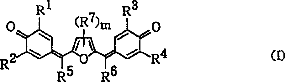
A highly sensitive positively charged type electrophotographic photoconductor includes an organic compound that transports electrons efficiently, improving light emission efficiency. The photoconductor is used in an electrophotographic drum, an electrophotographic cartridge and an electrophotographic apparatus. The photosensitive layer includes at least one compound represented by the following general formula (I) wherein each of R<1> to R<4>, is independently selected from the group consisting of hydrogen atoms, alkyl groups having 1-6 carbon atoms that optionally have substituents and aryl groups that optionally have substituents, each of R<5> and R<6> is independently selected from the group consisting of hydrogen atoms, alkyl groups having 1-6 carbon atoms that optionally have substituents, aryl groups that optionally have substituents and heterocyclic groups that optionally have substituents, R<7> is selected from the group consisting of halogen atoms, alkyl groups having 1-6 carbon atoms that optionally have substituents, aryl groups that optionally have substituents and heterocyclic groups that optionally have substituents, m represents an integer of 0 to 2. The electrophotographic photoreceptor and the electrophotographic device use the quinomethane compound.
Description
[technical field that the present invention belongs to]
The present invention relates to electrophotography photoconductor (following also abbreviate as " photoconductor "), be specifically related to electrophotography photoconductor with photographic layer, this photographic layer comprises the organic material on the conducting base, is used for similarly electrophotographic system such as printer, duplicating machine.
Secondly, the present invention relates to quinolmethane (quinomethane) compound, be specifically related to a kind of novel quinolmethane (quinomethane) compound that can be used as electrophotography photoconductor electron transport materials, a kind of Organnic electroluminescent device (EL) and similar device.
[prior art]
Before this, inorganic photoconductive material arranged, and, had a kind of inorganic photoconductive materials such as zinc paste, cadmium sulfide to be scattered in the material of making in the resin binder as selenium or selenium alloy as the photographic layer of electrophotography photoconductor is once used.In recent years, relevant electrophotography photoconductor aspect uses the research of organic photoconductive material to make progress, and some material has entered practical application, and light sensitivity and serviceable life all make moderate progress.
The function that requires photoconductor to have in the dark to keep surface charge, have and be subjected to the light time to produce the function of electric charge and have the similar function that is subjected to the light time transfer charge.Therefore, so-called individual layer photoconductor has just been arranged, and its one deck has promptly possessed these functions, and so-called laminar light electric conductor, its each layer has independent function: it is to produce electric charge that one deck mainly acts on, and one deck plays and in the dark keeps surface charge and in the effect that is subjected to the light time transfer charge.
In order to utilize this type of photoconductor to form image by electrophotography, but application card Ademilson system (Carlson system).This system charges with imaging by the method with corona discharge in the dark to photoconductor, the electrostatic image of source document character and picture etc. is formed on the surface of charging back photoconductor, with formed developing electrostatic images, the toner image photographic fixing after will developing again is to the propping material of paper one class with toner.After the toner image is transferred, photoconductor is handled removal electric charge, removal remaining toner, elimination exposure etc. use again with follow-up now.
Compare with inorganic photoconductor, the advantage that drops into the organic photoconductor of practice is that it is flexible, film forming good, cost is low, safe etc.In addition, because material is rich and varied, light sensitivity, serviceable life etc. has had further improvement.
Most of organic conductors are layer structures, and wherein the function of each layer is independent, is born by charge generating layers and charge transport layer respectively.Generally speaking, be formed with charge generating layers and charge transport layer on the matrix according to the order of sequence can conducting.Charge generating layers comprises that electric charge generates material, and as pigment or dyestuff, and charge transport layer comprises charge transport material, as hydrazone or triphenylamine.Thereby, bestow characteristic according to the electric charge of charge transport material, organic photoconductor becomes the hole transfevent, produces photosensitization when surperficial bear is electric.Yet, the comparing of electronegative type with the positively charged type, the used corona discharge method that charges is unsettled.In addition, the ozone of generation, oxides of nitrogen etc. are adsorbed on photoconductor surface, can cause physics and chemical property to degenerate.Therefore can cause ecological deterioration.In this respect, for photoconductor, the positively charged type uses more flexible than electronegative type, and range of application is wider, more has superiority.
Thereby, in order to make photoconductor become the positively charged type, proposed a kind of method and the practicality of part input, wherein electric charge generation material and charge transport material are dispersed in the resin binder simultaneously, are made into the photographic layer (photosensitive layer) of similar individual layer.Yet the light sensitivity deficiency of individual layer photoconductor can not be used in the high speed machines, and requires further improvement to improve stability or the like.
In addition, in order to provide the discrete layer structure of a kind of function in the hope of obtaining ISO, a kind of imagination is to make photoconductor by form a charge generating layers on charge transport layer, uses as the positively charged type.Yet,, will produce stability problem when carrying out corona discharge, rayed, mechanical wear etc. repeatedly because charge generating layers forms from the teeth outwards in this method.In this case, a protective seam is established in the suggestion that also has again outside charge generating layers.Though this has improved the anti-mechanical wear performance of structure, but still the unresolved problem of bringing such as the degeneration of electrical properties such as light sensitivity.
In addition, also propose a kind of method of making photoconductor, promptly on charge generating layers, formed a charge transport layer that possesses the electron transport characteristic.
As the charge transport material that possesses the electron transport characteristic, known example has 2,4,7-trinitro--9-Fluorenone (fluorenon) etc.Yet these materials are carcinogenic, and safety problem is arranged.In addition, at the open JP-A-1-206349 of Japan's special permission, JP-A-6-59483, JP-A-9-190002 has introduced cyanogen compound and naphtoquinone compounds among the JP-A-9-190003 etc.Yet, do not obtain any electron transport materials that is enough to drop into practical application as yet.
Secondly, a large amount of electron transport materials and use the electrophotography photoconductor of this material to cause concern, such as, be found in JP-A-4-360148, Journal of the Society of Electrophotographyof Japan, the 30th volume, the the 266th to 273 page (1991), JP-A-3-290666, JP-A-5-92936, Proceedings of Pan_pacific Imaging Conference/Japan Hardcopy ' 98,15-17 day in July, 1998,1998 JAHALL, Tokyo, 207-210 page or leaf (1998), JP-A-9-151157,97,1997 year July 9 of Proceedings of Japan Hardcopy ', 10,11, JAHALL (Otemachi, Tokyo), 173-176 page or leaf (1992), JP-A-10-73937, JP-A-4-338760, JP-A-1-230054, JP-A-8-278643, JP-A-2001-222122 etc. mention and describe.And, notice that unite the photoconductor light sensitivity height that uses hole material for transfer and electron transport materials in single photographic layer, part has entered practical application.So-called photoconductor is found in the open JP-A-5-150481 of Japan's special permission, JP-A-6-130688, JP-A-9-281728, JP-A-9-281729, JP-A-10-239874 etc.
In addition, have now and use the organic field luminescence body of organic photoconductive material to make light-emitting device, this type of device estimates to be used in the recent period display and so on.As for the organic field luminescence body, propose many suggestions and improved organic material, wherein some has dropped into practical application.
The simple structure form of organic field luminescence body is to place the luminescent layer that includes the organic compounds luminescent material between electrode, make and form electric current between the electrode, thereby cause electronics and hole and inject luminescent layer from electrode, form exciton in luminescent layer, compound (recombination) that brings produces luminous.In addition, inject the efficient of luminescent layer in order to guarantee electronics and hole, proposed a kind of structure, wherein the functional layer such as hole transfer layer, hole injection layer, electron supplying layer, electron injecting layer forms with luminescent layer.In each layer, electron supplying layer and electron injecting layer have used the organic compound that possesses the electron transport function (to participate in Ohmori, " Recent development of highly efficient organic EL materials; " OYO BUTURI, the 70th volume, the 12nd phase, 1419-1425 page or leaf (2001) etc.).
[the problem to be solved in the present invention]
In contrast, the inventor has proposed the multiple photoconductor that comprises the high-quality electron transport materials (for example at JP-A-2000-75520, JP-A-2000-199979, JP-A-2000-143607 and JP-A-2001-142239 etc. described in) so far.Yet the demand to the ISO photoconductor requires to produce the high-performance optical electric conductor that uses the stronger novel charge transport material of electron transport ability always recently.
For this reason, an object of the present invention is to provide a kind of ISO positively charged type photoconductor that is used for duplicating machine, printer by using the electron transport materials of a kind of unused so far novel organic compound as photographic layer.
In addition, when applying to organic field luminescence body (EL), also carry material to propose requirement, higher brightness can be provided, can improve luminescence efficiency high-performance electronic.
Therefore, an object of the present invention is to provide a kind of compound of electron transport function excellence, can be used for photoconductor and organic EL of electrofax.
[means of dealing with problems]
In order to achieve the above object, the inventor has furtherd investigate multiple organic material.Consequently, the inventor finds to use the specific compound of following general formula (I) expression, and this compound has the electron transport performance, can obtain the ISO photoconductor, can carry out the positive charge charging, thereby realize the present invention.
Promptly, in order to address the above problem, electrophotography photoconductor of the present invention is provided with on conductive base and comprises the photographic layer that electric charge generates material and charge transport material, it is characterized in that, this photographic layer comprises the compound of a kind of following general formula (I) expression at least:
In the molecular formula (I), R1, R2, R3 and R4 can be identical or different, the expression hydrogen atom, the alkyl that can have substituent 1 to 6 carbon atom maybe can have substituent aryl, R5 and R6, can be identical or different, the expression hydrogen atom, the alkyl that can have substituent 1 to 6 carbon atom, can have substituent aryl, perhaps can have substituent heterocycle group, R7 represents halogen atom, the alkyl that can have substituent 1 to 6 carbon atom, substituent aryl can be had and maybe substituent heterocycle group can be had, m represents 0 to 2 integer, a plurality of R7 can be identical or different, and substituting group is represented halogen atom, the alkyl of 1 to 6 carbon atom, the alkoxy of 1 to 6 carbon atom, with or without substituent aryl or with or without substituent heterocyclic radical.Substituting group represents the alkoxy of the alkyl of halogen atom, 1 to 6 carbon atom, 1 to 6 carbon atom, with or without substituent aryl or with or without substituent heterocyclic radical.
In addition, in order to address the above problem, compound of the present invention is a kind of quinolmethane (quinomethane) compound, it is characterized in that its structure represented by following general formula (I):
In the molecular formula (I), R1, R2, R3 and R4 can be identical or different, the expression hydrogen atom, the alkyl that can have substituent 1 to 6 carbon atom maybe can have substituent aryl, R5 and R6, can be identical or different, the expression hydrogen atom, the alkyl that can have substituent 1 to 6 carbon atom, can have substituent aryl, perhaps can have substituent heterocycle group, R7 represents halogen atom, the alkyl that can have substituent 1 to 6 carbon atom, can have substituent aryl and maybe can have substituent heterocycle group, m represents 0 to 2 integer, and a plurality of R7 can be identical or different.Substituting group represents the alkoxy of the alkyl of halogen atom, 1 to 6 carbon atom, 1 to 6 carbon atom, with or without substituent aryl or with or without substituent heterocyclic radical.
[embodiments of the present invention]
The instantiation of the compound of above-mentioned general formula (I) expression is found in following structural formula (I-1) to (I-59).Yet the present invention is not limited to these compounds.In following instantiation,
 The expression tert-butyl.


Quinolmethane (quinomethane) compound according to the present invention by above-mentioned general formula (I) expression has good electron transport performance.Therefore, these compounds can be used as so-called electron transport materials, particularly can be preferably used as the photochromics of electrophotography photoconductor, and the functional layer of the electron supplying layer of organic EL and so on.
Can come synthetic according to following reaction equation (1) according to compound of the present invention.Promptly; shown in following reaction equation (1); the compound of structural formula (I) expression synthetic can be by making following structural formula (A) and/or (A ') compound and following structural formula (B) compound usefulness proper metal organic reagent (for example; just-butyl lithium etc.) react; thereafter remove protecting group (TMS: trimethyl silicon based) thereby the compound of composite structure formula (C) expression, (C) compound further carries out dehydration condensation with suitable catalyzer (as the p-toluenesulfonic acid etc.).Carry one in passing, TBAF represents tetrabutylammonium in the following reaction equation (1).
In addition, the compound of structural formula (B) expression is synthetic can synthesize with the reaction of the furan compound of following structural formula (D) by making following structural formula (E) and/or following structural formula (the E ') compound of expression.Obtain the compound of following structural formula (E) and/or following structural formula (E ') expression can following structural formula (F) and/or the compound represented of following structural formula (F ') as parent material.Reaction equation (1)
 Followingly elaborate with reference to the embodiment of accompanying drawing to electrophotography photoconductor of the present invention.
[brief description of drawings]
Fig. 1: the cross sectional representation of one embodiment of the invention electrophotography individual layer photoconductor.
Fig. 2: the cross sectional representation of another embodiment of the present invention electrophotography laminar light electric conductor.
Fig. 3: the infrared spectrum of compound shown in the structural formula (I-5).
Fig. 4: compound shown in the structural formula (I-5)
1The H-NMR spectrum.
Fig. 5: the infrared spectrum of compound shown in the structural formula (I-27).
Fig. 6: compound shown in the structural formula (I-27)
1The H-NMR spectrum.
[drawing reference numeral and symbol description]
1 conductive base
2 photographic layers
3 charge generating layers
4 charge transport layers
5 photographic layers (layer structure)
6 protective seams
[file mark] accompanying drawing
[Fig. 3]
Transmissivity
Wave number
[Fig. 5]
Transmissivity
Wave number
Fig. 1 and Fig. 2 are the cross sectional representation of the various layouts of photoconductor.
Shown in Figure 1 is a kind of layout of individual layer photoconductor.Conductive base 1 is provided with individual layer photographic layer 2, is that electric charge generates material and charge transport material is scattered in (a kind of bonding agent) in the resin binder, and external coating 6 (protective seam) is arranged on it, and this is that the making photoconductor is needed.Make the individual layer photoconductor and electric charge can be generated dispersion of materials in the solution that has dissolved charge transport material and resin binder, then dispersion liquid is applied on the conductive base.In addition, can form external coating 6 in the above in case of necessity.
Shown in Figure 2 is a kind of layout of laminar light electric conductor.Conductive base 1 is provided with photographic layer 5, and wherein charge generating layers 3 generates material based on electric charge, and charge transport layer 4 comprises charge transport material, and stratification constitutes photoconductor in order.Make the stratiform photoconductor and can on conductive base, form charge generating layers, electric charge generates and carries out drying after material adopts vacuum evaporation deposition or applies dispersion liquid, and dispersion liquid intersperses among electric charge generation material in solvent or the resin binder and prepares; And then on charge generating layers, form charge transport layer, and take to apply solvent and carry out dry method, be dissolved with charge transport material and resin binder in this solvent.
In addition, although do not illustrate, can between conductive base and photographic layer, be provided with internal coating in the photoconductor of any kind.Internal coating is set satisfies following purpose: prevent that unexpected electric charge from injecting photographic layer, coated substrates flaw, strengthening the adhesive property of photographic layer from conductive base, or the like.Internal coating comprises that one deck is Main Ingredients and Appearance with the resin, one deck oxidation film such as anodized aluminum film, or similar material.
Moreover the various types of photoconductors of the present invention comprise at least a compound with electron transport performance of the present invention as charge transport material, and each compound is all used above-mentioned general formula (I) expression.
Describe below in conjunction with the better embodiment of accompanying drawing 2 laminar light electric conductors electrophotography photoconductor of the present invention.Yet the present invention is not limited to following specific embodiment.
The method that forms charge generating layers 3 is to use electric charge generation material particle is dispersed in the material that forms in the resin binder by preceding method, perhaps by vacuum evaporation material is deposited, and is subjected to light to produce electric charge.In addition, importantly the electric charge formation efficiency of charge generating layers 3 wants high, and possesses simultaneously the performance of the electric charge iunjected charge transfer layer 4 that is produced.In addition, wish that the electric field dependence of charge generating layers 3 is low, though under low electric field action also iunjected charge smoothly.
Generate material as for electric charge, used phthalocyanine compound, as metal-free phthalocyanine and TiOPc, various azos, quinone, indigo, cyanine, squarillium, azulene (azulenium), Evil English compound pigment or dyestuffs such as (pyrillium), selenium or selenium compound can therefrom be selected the material that is fit to according to the exposure wavelength scope of imaging.Unique necessity be that charge generating layers has the electric charge systematic function.Therefore, the thickness of film generates the absorption coefficient of light decision of material by electric charge, usually smaller or equal to 5 μ m, preferably in the 2 μ m.In addition, used charge generating layers can be that to generate material be Main Ingredients and Appearance and be added with composition such as charge transport material with electric charge.
For the resin binder of charge generating layers 3 usefulness, can use after polymkeric substance such as polycarbonate, polyester, polyamide, Polyurethane, vinyl chloride, phenoxy resin, polyvinyl butyral, diallyl phthalate resin or methacrylate and the multipolymer appropriate combination.
Charge transport layer 4 is that a charge transport material is scattered in the film that applies in the resin binder.In the dark, transfer layer stays the electric charge of holding photoconductor to become insulation course, and when being subjected to the light time, then shows the function of transfer charge, with the charge transport of charge generating layers injection.As mentioned before, the present invention need comprise at least a compound that possesses the electron transport performance as charge transport material, and this compound can be represented with general formula of the present invention (I).Yet, can also comprise another kind of charge transport material.According to the present invention, the preferable addition of this compound is the 10%-60% percentage by weight that accounts for charge transport layer 4 total amount of material, more preferably 15%-50% percentage by weight.
For the resin binder of charge transport layer 4, can use polymkeric substance such as polycarbonate, polyester, polyamide, polystyrene, methacrylate and multipolymer and so on.
In addition, hinder the photoconductor application, can in charge transport layer 4, add a series of antioxidants, as amine series, phenol series, sulphur series, phosphite series, phosphorus series etc. in order to prevent the degeneration that ozone causes.
Although the film thickness of coat itself is relevant with the composition of coat, can be within the specific limits determine arbitrarily, should not cause adverse effect in this scope, rest potential rising etc. when using repeatedly continuously.
Under the situation of individual layer photoconductor as shown in Figure 1, also need in photographic layer 2, comprise at least a The compounds of this invention that possesses the electron transport performance, this compound can be represented with general formula of the present invention (I).Yet, can use and identical other material of above-mentioned laminar light electric conductor, be not limited to them.As charge transport material, contain the compound of above-mentioned general formula (I) expression when preferably comprising the hole material for transfer.As the hole material for transfer, preferred benzidine derivative, triphenylamine derivative etc.In this case, the percentage by weight that the preferred addition of material accounts for the total amount of material of film forming photographic layer is preferably 10%-60% compound of the present invention, is more preferably 15%-50%.About the hole material for transfer, consumption is the 10%-60% percentage by weight preferably, more preferably the 20%-50% percentage by weight.
[embodiment]
Below embodiments of the invention are described.
The TiOPc of two parts of weight (TiOPc), the compound of said structure formula (I-5) expression of 40 parts of weight, the triphenylamine derivative of 60 parts of weight is as the hole material for transfer, and molecular formula is as follows
Polycarbonate resin (BP-PC: the emerging product of bright dipping company product) in mixer, knead 3 hours preparation coating liquids with 80 parts of weight with methylene chloride.Coating liquid is applied on the aluminium matter stilt and forms photographic layer, thereby makes the thickness of dry caudacoria reach 20 μ m, produces the individual layer photoconductor thus.
Photoconductor embodiment 2
Adopt with method identical in the embodiment 1 of photoconductor and make the individual layer photoconductor, different is the compound that replaces said structure formula (I-5) with the compound of above-mentioned structural formula (I-7).
Adopt with method identical in the embodiment 1 of photoconductor and make the individual layer photoconductor, different is the squarillium compound of representing with following molecular formula
Replace TiOPc, replace the compound of said structure formula (I-5) with the compound of above-mentioned structural formula (I-10).
Photoconductor embodiment 4
The x-type of two parts of weight is containing metal phthalocyanine (H2Pc) not, the compound of said structure formula (I-12) expression of 40 parts of weight, and the benzidine derivative of 60 parts of weight is as the hole material for transfer, and molecular formula is as follows
In mixer, knead 3 hours preparation coating liquids with the polycarbonate resin (PCZ200:Mitsubishi Gas Chemical Co., Ltd. produces) of 100 parts of weight with methylene chloride.Coating liquid is applied on the aluminium matter stilt and forms photographic layer, thereby makes the thickness of dry caudacoria reach 25 μ m, produces the individual layer photoconductor thus.
Photoconductor embodiment 5
Adopt with method identical in the embodiment 1 of photoconductor and make the individual layer photoconductor, different is the disazo pigment of representing with following molecular formula
 Replace TiOPc.
Adopt with method identical in the embodiment 1 of photoconductor and make the individual layer photoconductor, different is the disazo pigment of representing with following molecular formula
Replace TiOPc, replace the compound of said structure formula (I-5) with the compound of above-mentioned structural formula (I-16).
Electrofax characteristic to the photoconductor that above each embodiment obtained detects.
In the dark carry out corona discharge when making photoconductor surface positively charged with the voltage of+4.5 kilovolts, the initial surface electromotive force is made as Vs (V), stop at corona discharge subsequently, photoconductor in the dark keeps surface measurements electromotive force Vd (V) after 5 seconds.Next, with white light a period of time (is unit with the second) of illumination 100 luxs, Vd reduces half up to survey, gets and makes light sensitivity E1/2 (lux second).In addition, each of embodiment 1 to 4 has all been surveyed the time (second) that monochromatic light (780 nanometer) when irradiation Vd of 1 μ W reduces by half, and obtains light sensitivity E1/2 (μ J/cm according to the time
2).Moreover, to each embodiment, all surveyed rest potential Vr (V) after 10 seconds at white light or monochromatic light irradiation photoconductor surface.Testing result is as shown in table 1:
[table 1]
Synthetic embodiment 1: synthetic above-mentioned particular compound (I-5)<reaction equation (1-1) 〉

| White light | 780nm monochromatic light | |||
| Light sensitivity (lux second) | Rest potential (V) | Light sensitivity (μ J/cm 2) | Rest potential (V) | |
| | ????1.0 | ????70 | ????0.8 | ????60 |
| Embodiment 2 | ????1.3 | ????90 | ????1.1 | ????80 |
| | ????0.8 | ????50 | ????0.5 | ????40 |
| Embodiment 4 | ????1.2 | ????60 | ????0.7 | ????60 |
| Embodiment 5 | ????1.2 | ????80 | ?????- | ????- |
| | ????1.6 | ????90 | ?????- | ????- |
(step 1.)
Raw material, reagent
N, O-dimethyl azanol hydrochloride 220 mMs (21.5 gram)
(N,O-dimethylhydroxylamine?hydrochloride)
200 milliliters of methylene chloride
Pyridine 460 mMs (36.4 gram)
<operation 〉
(1) be placed with 4-chlorobenzoyl chloride and N in the three-necked bottle, the O-dimethyl azanol hydrochloride adds methylene chloride (200 milliliters).
Under (2) 0 ℃ (ice bath), the blanket of nitrogen with splashing into pyridine in 30 minutes, then stirring at room two hours.
(3) add about 100 ml waters and finish reaction, the extraction organic layer.With 100 milliliters of aqueous layer extracted of methylene chloride, reinstate the 1N hydrochloric acid solution with above organic layer one and clean, concentrate then.
(4) by column chromatography (silica gel, moving phase: methylene chloride) separation, purifying oily matter.
The result has obtained N-methoxyl N-methyl-benzamide.
Output is 33.3 grams (83.4% yield), MS m/z165 (M+).
(step 2.)
Raw material, reagent
<operation〉be placed with furans and tetramethyl ethyl diamines in (1) three-necked bottle, add hexane.Just splashing into-butyl lithium with 15 minutes under (2) 0 ℃ (ice bath), the blanket of nitrogen, stirring 30 minutes, stirring at room 30 minutes, heat cycles was 30 minutes more then.
| Furans | 30 mMs (2.04 gram) |
| Tetramethyl ethyl diamines | 66 mMs (7.67 gram) |
| Hexane | 20 milliliters |
| Just-butyl lithium (1.6M hexane solution) | 66 mMs (41 milliliters) |
| THF (tetrahydrofuran) | 75 milliliters |
| N-methoxyl-N-methyl-benzamide | 75 mMs (12.4 gram) |
| THF (tetrahydrofuran) | 20 milliliters |
(3), add THF (75 milliliters) with above-mentioned reactant liquor cool to room temperature.
℃ (4)-40 under-30 ℃ (dry ice-ethanol bath), the blanket of nitrogen with the THF solution that splashed into N-methoxyl-N-methyl-benzamide in 15 minutes, stirred 1 hour.
(5) reactant liquor slowly is cooled to room temperature, stirs 30 minutes.
(6) reactant liquor is poured in the frozen water and is stirred.
(7) filtering precipitate washs with ethanol.
More than the result of (step 1. 2.) obtained 2 of above-mentioned molecular formula (B-1) expression, 5-dibenzoyl furans.Output is 2.3 grams (27.7% yield), MS m/z276 (M+).(step is 3.)<raw material, reagent〉4-bromo-2,6-two tert-butyl-1-[trimethyl silyl]-benzene (A-1) 45 mMs (16.1 gram)
| THF (tetrahydrofuran) | 90 milliliters |
| Just-butyl lithium (1.6M hexane solution) | 54 mMs (34 milliliters) |
| 2,5-dibenzoyl furans (B-1) | 15 mMs (4.1 gram) |
| THF (tetrahydrofuran) | 30 milliliters |
| Aqueous | 10 milliliters |
| Tetrabutyl ammonium fluoride (1.0M THF solution) (TBAF) | 45 mMs (45 milliliters) |
| P-benzene methanesulfonic acid monohydrate (p-TsOH) | On a small quantity |
| Toluene | 100 milliliters |
<operation 〉
(1) puts into three-necked bottle after above-claimed cpd (A-1) is weighed, add THF (90 milliliters).
(2) under-78 ℃ (do-ice-ethanol bath), blanket of nitrogen, splashed into the n-butyl lithium, stirred 30 minutes, then stirring at room 30 minutes with 30 minutes.Then, the THF solution of above-claimed cpd (B-1) (30 milliliters) splashed into 30 minutes, stirred under the same conditions 3 hours.
(3) adding about 10 milliliters of ammonium chloride saturated aqueous solutions is hydrolyzed.
(4) 0 ℃ (ice bath), adding TBAF (45 milliliters) stirred 3 minutes.
(5) obtaining is that reactant liquor is poured frozen water into, stirs.
(6) use dichloromethane extraction, and extracting substance is concentrated.
(7) solid matter is dissolved in toluene (100 milliliters).Add a small amount of p-TsOH to solution, heat then and circulated 2 hours.
(8) after reaction is finished, concentrated solution.
(9) filter out solid matter, use a small amount of hexane wash, use the hexane recrystallization then.
Step result has 3. obtained the compound of above-mentioned molecular formula (I-5) expression.Output is 6.6 grams (67.4% yield), MS m/z652 (M+).The infrared spectrum of particular compound (I-5) as shown in Figure 3,
1The H-NMR spectrum as shown in Figure 4.
Synthetic embodiment 2: synthetic above-mentioned particular compound (I-27)<reaction equation (1-2) 〉
 Except replace the chlorobenzoyl chloride in the foregoing
 description 1 with the 4-chlorobenzoyl chloride, adopt identical operations to prepare the compound of above-mentioned molecular formula (I-27) expression.Output is 5.4 grams (50.1% yield), m/z720 (M+).The infrared spectrum of particular compound (I-27) as shown in Figure 5,
1The H-NMR spectrum as shown in Figure 6.
In addition, 4-bromo-2,6-two-tert-butyl-1-[trimethyl silyl]-benzene (above-mentioned molecular formula A-1) can synthesize with known method, the method for introducing such as the open JP-A-2001-222122 of Japan's special permission etc.
Photoconductor embodiment 7
Produced the drum-type photoconductor (30 millimeters φ) that is used to assess the disc type photoconductor of photoconductor electrical characteristics and estimates printing.
The internal coating solution of the following composition of dip-coating on aluminium dish and aluminum pipe respectively in 100 ℃ of dryings 60 minutes, forms internal coating film thickness 0.3 μ m then.Following term " part " expression weight portion:
3 parts of solvable nylon (Amyran CM8000: the beautiful industry in east is produced)
(5/5) 97 part of ethanol/methylene mixed dissolution
Subsequently, forming single photographic layer film thickness in 60 minutes in 100 ℃ of dryings after the dispersion liquid dip-coating that the individual layer photographic layer is used is 25 μ m, its composition such as following:
Electric charge generates material: 0.3 part of the metal-free phthalocyanine of X-type
Hole material for transfer: the triphenylamine derivative of structural formula (HT1) expression
Electron transport materials: the compound of molecular formula (I-5) expression
(synthetic embodiment 1) 3 parts
Antioxidant: 3,5-two-uncle-4-hydroxy-methylbenzene (BHT)
(Tokyo chemical industry product) 1 part
0.01 part of silicone oil: KF-50 (crescent chemical industry product)
Binder resin: bis-phenol z-type polycarbonate resin
(Panlite TS2020:Teijin Chemical Co., Ltd. produces) 10 parts
100 parts of methylene chloride
Made the electrophotography photoconductor according to said method.
Except replacing the electron transport materials of 3 parts of above-mentioned molecular formula (I-5) by electron transport materials synthetic among the synthetic embodiment 2, adopt the method identical to prepare photoconductor with photoconductor embodiment 1 with above-mentioned molecular formula (I-27) expression with the composition of the dispersion liquid of preparation photographic layer used among 3 parts of photoconductor embodiment 1.
The assessment of embodiment 7,8 photoconductors
In order to assess its electrical characteristics, the disc type photoconductor is carried out in the EPA-8100 type electro-photographic paper tester that Co., Ltd. of the electric making of Kawaguchi institute produces.
23 ℃ of environment temperatures, humidity 45% make each photoconductor charged in the dark place, surface potential reaches+600V, are calculated as follows to the surface potential sustainment rate that obtains to expose 5 preceding seconds thereafter:
Sustainment rate V
K5(%)=(V5/V0) * 100 wherein
V0: the instant surface potential after the exposure;
The surface potential (expose initial) of V5:5 after second.
After this, surface potential is reached+600V, with 1.0 μ W/cm with same procedure
2Monochromatic light exposes, and is separated obtaining 780nm wavelength, 5 seconds time shutter from Halogen lamp LED by light filter.Make that surface potential reduces by half (+300V) required exposure is measured and is made light sensitivity E
1/2(μ J/cm
2), the back 5 seconds surface potential that exposes is got and is made rest potential Vr (V).Assessment result is as shown in table 2.
[table 2]
| Sustainment rate V k5????(%) | Light sensitivity E 1/2(μJ/cm 2) | Rest potential Vr (V) | |
| Photoconductor embodiment 7 | ????85.2 | ????0.48 | ????66 |
| | ????82.5 | ????0.42 | ????57 |
Be the permanance of assessment actual print, the drum-type photoconductor is installed on the HL-1240 type laser printer of Brother Industries Ltd's product, has printed complete black figure, Quan Baitu, each portion of half chromatic graph under the condition of 25 ℃ of environment temperatures, humidity 52%.After this, printed the image of 5000 seal rates about 5%.Thereafter, each seal portion is deceived figure, Quan Baitu and half chromatic graph entirely again, so that situation about printing after 5000 is assessed.
As a result, embodiment 7 and 8 the initial image of photoconductor and print 5000 after image all be good.
[effect of invention]
As previously discussed, according to the present invention, be arranged on and used the represented compound that possesses the electron transport performance of above general formula (I) as charge transport material in the photosensitive layer on the conductive base, obtained thus the photoconductor that speed is high when positively charged, electrical characteristics are excellent. In addition, for the electric charge generating material, can select suitable material according to exposure light. Therefore, use phthalocyanine compound, squarillium compound, bis-azo compound etc. can obtain photoconductor and be used for semiconductor laser printer and duplicator. In addition, being provided with from the teeth outwards as required coat can increase the service life.
In addition, the compound that the present invention can electron gain transportation performance excellence. These compounds for the electronic installation that uses organic compound, such as electrophotography photoconductor and organic field luminescence body, can be improved the performances such as electrical characteristics and luminous efficiency.
Claims (4)
1. an electrophotography photoconductor wherein is provided with the photographic layer that comprises electric charge generation material and charge transport material on conductive base, and it is characterized in that: this photographic layer comprises the compound of at least a following general formula (I) expression:
In the molecular formula (I), R1, R2, R3 and R4 can be identical or different, the expression hydrogen atom, the alkyl that can have substituent 1 to 6 carbon atom maybe can have substituent aryl, R5 and R6, can be identical or different, the expression hydrogen atom, the alkyl that can have substituent 1 to 6 carbon atom, can have substituent aryl, perhaps can have substituent heterocycle group, R7 represents halogen atom, the alkyl that can have substituent 1 to 6 carbon atom, substituent aryl can be had and maybe substituent heterocycle group can be had, m represents 0 to 2 integer, a plurality of R7 can be identical or different, and substituting group is represented halogen atom, the alkyl of 1 to 6 carbon atom, the alkoxy of 1 to 6 carbon atom, with or without substituent aryl or with or without substituent heterocyclic radical.
2. a quinolmethane (quinomethane) compound is characterized in that: the structure that following general formula (I) expression is arranged:
 In the molecular formula (I), R1, R2, R3 and R4 can be identical or different, the expression hydrogen atom, the alkyl that can have substituent 1 to 6 carbon atom maybe can have substituent aryl, R5 and R6, can be identical or different, the expression hydrogen atom, the alkyl that can have substituent 1 to 6 carbon atom, can have substituent aryl, perhaps can have substituent heterocycle group, R7 represents halogen atom, the alkyl that can have substituent 1 to 6 carbon atom, substituent aryl can be had and maybe substituent heterocycle group can be had, m represents 0 to 2 integer, a plurality of R7 can be identical or different, and substituting group is represented halogen atom, the alkyl of 1 to 6 carbon atom, the alkoxy of 1 to 6 carbon atom, with or without substituent aryl or with or without substituent heterocyclic radical.
3. electrophotography photoconductor as claimed in claim 1, it is characterized in that: described photographic layer is the individual layer photographic layer.
4. an electro-photography apparatus is characterized in that: comprise as claim 1 or 3 described electrophotography photoconductors, and charging process is to realize by filling with positive charge.
Applications Claiming Priority (4)
| Application Number | Priority Date | Filing Date | Title |
|---|---|---|---|
| JP2002154097 | 2002-05-28 | ||
| JP2002154097 | 2002-05-28 | ||
| JP2003105039A JP3937336B2 (en) | 2002-05-28 | 2003-04-09 | Quinomethane compound, electrophotographic photoreceptor and electrophotographic apparatus |
| JP2003105039 | 2003-04-09 |
Publications (1)
| Publication Number | Publication Date |
|---|---|
| CN1461978A true CN1461978A (en) | 2003-12-17 |
Family
ID=29782000
Family Applications (1)
| Application Number | Title | Priority Date | Filing Date |
|---|---|---|---|
| CN03138554A Pending CN1461978A (en) | 2002-05-28 | 2003-05-28 | Photoconductor and quinolmethane compound for electronic photograph |
Country Status (5)
| Country | Link |
|---|---|
| US (1) | US6933091B2 (en) |
| JP (1) | JP3937336B2 (en) |
| KR (1) | KR20030091818A (en) |
| CN (1) | CN1461978A (en) |
| DE (1) | DE10323211A1 (en) |
Cited By (1)
| Publication number | Priority date | Publication date | Assignee | Title |
|---|---|---|---|---|
| CN104345584A (en) * | 2013-07-31 | 2015-02-11 | 京瓷办公信息系统株式会社 | Electrophotographic photosensitive member and image forming apparatus |
Families Citing this family (2)
| Publication number | Priority date | Publication date | Assignee | Title |
|---|---|---|---|---|
| DE112004002245T5 (en) * | 2003-11-28 | 2006-11-09 | Fuji Electric Holdings Co., Ltd., Kawasaki | switching device |
| JP5123676B2 (en) * | 2007-02-07 | 2013-01-23 | 京セラドキュメントソリューションズ株式会社 | Electrophotographic photoreceptor and color image forming apparatus |
Family Cites Families (26)
| Publication number | Priority date | Publication date | Assignee | Title |
|---|---|---|---|---|
| JP2718048B2 (en) | 1988-02-15 | 1998-02-25 | 株式会社ブリヂストン | Charge transport agent for electrophotographic photosensitive member and electrophotographic photosensitive member |
| JPH01230054A (en) | 1988-03-10 | 1989-09-13 | Mitsui Toatsu Chem Inc | Electrophotographic sensitive body |
| EP0449565B1 (en) * | 1990-03-26 | 1997-05-14 | Matsushita Electric Industrial Co., Ltd. | Photosensitive material for electrophotography |
| JP2805376B2 (en) | 1990-04-09 | 1998-09-30 | キヤノン株式会社 | Organic electronic materials |
| JP3113313B2 (en) | 1991-06-07 | 2000-11-27 | 京セラミタ株式会社 | Organic photoconductor for electrophotography |
| JP3124056B2 (en) | 1991-04-05 | 2001-01-15 | 京セラミタ株式会社 | Photoreceptor using dinaphthoquinone derivative |
| JPH04338760A (en) | 1991-05-15 | 1992-11-26 | Konica Corp | Electrophotographic sensitive body |
| JP3105602B2 (en) | 1991-11-29 | 2000-11-06 | 京セラミタ株式会社 | Electrophotographic photoreceptor |
| JP2587748B2 (en) | 1992-02-07 | 1997-03-05 | 株式会社巴川製紙所 | Fluorenone derivative and laminated electrophotographic photosensitive member using the same |
| JPH0659483A (en) | 1992-08-04 | 1994-03-04 | Ricoh Co Ltd | Electrophotographic sensitive body |
| JPH06130688A (en) | 1992-10-05 | 1994-05-13 | Mita Ind Co Ltd | Electrophotographic sensitive body |
| JPH07179775A (en) | 1993-12-24 | 1995-07-18 | Tomoegawa Paper Co Ltd | Fluorenone derivative and laminated electrophotographic photoreceptor using the same |
| JPH08278643A (en) | 1995-04-10 | 1996-10-22 | Mita Ind Co Ltd | Electrophotographic organic photoreceptor |
| JP3471163B2 (en) | 1995-09-25 | 2003-11-25 | 京セラミタ株式会社 | Naphthoquinone derivative and electrophotographic photoreceptor using the same |
| US5631114A (en) | 1995-12-21 | 1997-05-20 | Hewlett-Packard Company | Derivatives of diiminoquinones useful as electron transport agents in electrophotographic elements |
| US5558965A (en) | 1995-12-21 | 1996-09-24 | Hewlett-Packard Company | Diiminoquinilidines as electron transport agents in electrophotographic elements |
| JP3273542B2 (en) | 1996-04-12 | 2002-04-08 | キヤノン株式会社 | Electrophotographic photoreceptor, process cartridge having the electrophotographic photoreceptor, and electrophotographic apparatus |
| JP3273543B2 (en) | 1996-04-12 | 2002-04-08 | キヤノン株式会社 | Electrophotographic photoreceptor, process cartridge having the electrophotographic photoreceptor, and electrophotographic apparatus |
| JP2997735B2 (en) | 1996-06-26 | 2000-01-11 | 富士電機株式会社 | Electrophotographic photoreceptor |
| JP3272257B2 (en) | 1997-02-26 | 2002-04-08 | 京セラミタ株式会社 | Electrophotographic photoreceptor |
| JP3666262B2 (en) | 1998-08-27 | 2005-06-29 | 富士電機デバイステクノロジー株式会社 | Electrophotographic photoreceptor |
| JP2000143607A (en) | 1998-09-04 | 2000-05-26 | Fuji Electric Co Ltd | Electron transporting material, electrophotographic photoreceptor and electrophotographic apparatus |
| JP3717320B2 (en) | 1998-10-29 | 2005-11-16 | 富士電機画像デバイス株式会社 | Electrophotographic photoreceptor |
| JP2001142239A (en) | 1999-11-17 | 2001-05-25 | Fuji Denki Gazo Device Kk | Electrophotographic photoreceptor |
| JP3355173B2 (en) | 1999-11-30 | 2002-12-09 | 京セラミタ株式会社 | Electrophotographic photoreceptor using quinone derivative |
| JP2002037755A (en) | 2000-07-26 | 2002-02-06 | Kyocera Mita Corp | Ketone derivative and electrophotographic photoreceptor using the same |
-
2003
- 2003-04-09 JP JP2003105039A patent/JP3937336B2/en not_active Expired - Fee Related
- 2003-05-22 DE DE10323211A patent/DE10323211A1/en not_active Withdrawn
- 2003-05-23 US US10/444,094 patent/US6933091B2/en not_active Expired - Fee Related
- 2003-05-27 KR KR10-2003-0033672A patent/KR20030091818A/en not_active Application Discontinuation
- 2003-05-28 CN CN03138554A patent/CN1461978A/en active Pending
Cited By (2)
| Publication number | Priority date | Publication date | Assignee | Title |
|---|---|---|---|---|
| CN104345584A (en) * | 2013-07-31 | 2015-02-11 | 京瓷办公信息系统株式会社 | Electrophotographic photosensitive member and image forming apparatus |
| CN104345584B (en) * | 2013-07-31 | 2018-06-26 | 京瓷办公信息系统株式会社 | Electrophtography photosensor and image forming apparatus |
Also Published As
| Publication number | Publication date |
|---|---|
| JP2004054222A (en) | 2004-02-19 |
| US20040033430A1 (en) | 2004-02-19 |
| KR20030091818A (en) | 2003-12-03 |
| US6933091B2 (en) | 2005-08-23 |
| JP3937336B2 (en) | 2007-06-27 |
| DE10323211A1 (en) | 2004-01-29 |
Similar Documents
| Publication | Publication Date | Title |
|---|---|---|
| JP5494844B2 (en) | Electrophotographic photosensitive member, electrophotographic photosensitive member cartridge, and image forming apparatus | |
| JPH0721646B2 (en) | Electrophotographic photoreceptor | |
| JP2000199979A (en) | Electrophotographic photoreceptor | |
| JPS61148159A (en) | Multilayer photosensitive imaging member containing sulfur-containing dicyanomethylene fluorenecarboxylate compound | |
| CN101371201A (en) | Quinone compound, photoreceptor for electrophotography, and electrophotographic device | |
| CN1881092A (en) | Electrophotographic photoreceptor and electrophotographic imaging apparatus using the photoreceptor | |
| CN1437074A (en) | Electrophotographical photoreceptor and electronic photographic equipment using the same photoreceptor | |
| CN1303030A (en) | Photoelectric conductor for electrophotography | |
| CN1461978A (en) | Photoconductor and quinolmethane compound for electronic photograph | |
| US6472514B2 (en) | Electron transport compounds | |
| CN1326118A (en) | Electronic camera photoelectric conductor | |
| CN1163798C (en) | Electrophotographic Photoconductor | |
| JP2014095867A (en) | Electrophotographic photoreceptor and image forming apparatus | |
| CN1078714C (en) | Photosensitive member for electrophotography | |
| CN1296198A (en) | Electronic photographic photosensitive material, electronic photographic photoelectric conductor and making method thereof | |
| JP2000075520A (en) | Electrophotographic photoreceptor | |
| CN1405636A (en) | Single-layer organic photosensitive object with positive charge for liquid developing | |
| US20030195359A1 (en) | Quinomethane compounds | |
| CN1573599A (en) | Novel charge transport materials having heteroaromatic hydrazone groups | |
| CN1523453A (en) | Polymer having stilbenquinone structure and electrophotographic photoreceptor containing the same | |
| JP2005035980A (en) | Quinone compound | |
| JP2005037476A (en) | Electrophotographic photoreceptor | |
| CN1713079A (en) | Electrophotographic photoreceptor and image forming apparatus provided with the same | |
| JPWO2005003093A1 (en) | Novel compound, electrophotographic photoreceptor and electrophotographic apparatus using the same | |
| JP2002221809A (en) | Electrophotographic photoreceptor |
Legal Events
| Date | Code | Title | Description |
|---|---|---|---|
| C06 | Publication | ||
| PB01 | Publication | ||
| C10 | Entry into substantive examination | ||
| SE01 | Entry into force of request for substantive examination | ||
| C02 | Deemed withdrawal of patent application after publication (patent law 2001) | ||
| WD01 | Invention patent application deemed withdrawn after publication |