CN1437773A - Multilayer structures as stable hole-injecting electrodes for use in high efficiency organic electronic device - Google Patents
Multilayer structures as stable hole-injecting electrodes for use in high efficiency organic electronic device Download PDFInfo
- Publication number
- CN1437773A CN1437773A CN01811439A CN01811439A CN1437773A CN 1437773 A CN1437773 A CN 1437773A CN 01811439 A CN01811439 A CN 01811439A CN 01811439 A CN01811439 A CN 01811439A CN 1437773 A CN1437773 A CN 1437773A
- Authority
- CN
- China
- Prior art keywords
- layer
- pani
- conductivity
- pedt
- polymer
- Prior art date
- Legal status (The legal status is an assumption and is not a legal conclusion. Google has not performed a legal analysis and makes no representation as to the accuracy of the status listed.)
- Granted
Links
- 229920000767 polyaniline Polymers 0.000 claims description 129
- 239000000203 mixture Substances 0.000 claims description 85
- 239000000463 material Substances 0.000 claims description 58
- 238000002347 injection Methods 0.000 claims description 16
- 239000007924 injection Substances 0.000 claims description 16
- 239000011368 organic material Substances 0.000 claims description 16
- 229920000620 organic polymer Polymers 0.000 claims description 12
- 229920001940 conductive polymer Polymers 0.000 claims description 9
- 239000010410 layer Substances 0.000 abstract description 236
- 229920000642 polymer Polymers 0.000 abstract description 80
- 239000012044 organic layer Substances 0.000 abstract 2
- 229920001609 Poly(3,4-ethylenedioxythiophene) Polymers 0.000 description 89
- -1 poly(ethylenedioxythiophene) Polymers 0.000 description 62
- 229920002401 polyacrylamide Polymers 0.000 description 43
- 239000000243 solution Substances 0.000 description 30
- XLYOFNOQVPJJNP-UHFFFAOYSA-N water Substances O XLYOFNOQVPJJNP-UHFFFAOYSA-N 0.000 description 26
- 239000010408 film Substances 0.000 description 25
- 125000000217 alkyl group Chemical group 0.000 description 24
- 239000002253 acid Substances 0.000 description 17
- 125000004432 carbon atom Chemical group C* 0.000 description 17
- 229910052751 metal Inorganic materials 0.000 description 16
- 239000002184 metal Substances 0.000 description 16
- 239000000758 substrate Substances 0.000 description 15
- 229920000547 conjugated polymer Polymers 0.000 description 14
- 229920000553 poly(phenylenevinylene) Polymers 0.000 description 13
- 125000003545 alkoxy group Chemical group 0.000 description 12
- CSCPPACGZOOCGX-UHFFFAOYSA-N Acetone Chemical compound CC(C)=O CSCPPACGZOOCGX-UHFFFAOYSA-N 0.000 description 11
- PAYRUJLWNCNPSJ-UHFFFAOYSA-N N-phenyl amine Natural products NC1=CC=CC=C1 PAYRUJLWNCNPSJ-UHFFFAOYSA-N 0.000 description 11
- 150000001732 carboxylic acid derivatives Chemical class 0.000 description 11
- YMWUJEATGCHHMB-UHFFFAOYSA-N Dichloromethane Chemical compound ClCCl YMWUJEATGCHHMB-UHFFFAOYSA-N 0.000 description 9
- YXFVVABEGXRONW-UHFFFAOYSA-N Toluene Chemical compound CC1=CC=CC=C1 YXFVVABEGXRONW-UHFFFAOYSA-N 0.000 description 9
- 229910052782 aluminium Inorganic materials 0.000 description 9
- XAGFODPZIPBFFR-UHFFFAOYSA-N aluminium Chemical compound [Al] XAGFODPZIPBFFR-UHFFFAOYSA-N 0.000 description 9
- 125000003118 aryl group Chemical group 0.000 description 9
- 125000000732 arylene group Chemical group 0.000 description 9
- 229920001577 copolymer Polymers 0.000 description 9
- 229910052736 halogen Inorganic materials 0.000 description 9
- 150000002739 metals Chemical class 0.000 description 9
- 238000000034 method Methods 0.000 description 9
- 239000002904 solvent Substances 0.000 description 9
- BQCADISMDOOEFD-UHFFFAOYSA-N Silver Chemical compound [Ag] BQCADISMDOOEFD-UHFFFAOYSA-N 0.000 description 8
- 150000007513 acids Chemical class 0.000 description 8
- 150000002367 halogens Chemical class 0.000 description 8
- 229910052709 silver Inorganic materials 0.000 description 8
- 239000004332 silver Substances 0.000 description 8
- PXHVJJICTQNCMI-UHFFFAOYSA-N Nickel Chemical compound [Ni] PXHVJJICTQNCMI-UHFFFAOYSA-N 0.000 description 7
- 125000004093 cyano group Chemical group *C#N 0.000 description 7
- APFVFJFRJDLVQX-UHFFFAOYSA-N indium atom Chemical compound [In] APFVFJFRJDLVQX-UHFFFAOYSA-N 0.000 description 7
- 238000004519 manufacturing process Methods 0.000 description 7
- 238000005259 measurement Methods 0.000 description 7
- UHOVQNZJYSORNB-UHFFFAOYSA-N Benzene Chemical compound C1=CC=CC=C1 UHOVQNZJYSORNB-UHFFFAOYSA-N 0.000 description 6
- LSNNMFCWUKXFEE-UHFFFAOYSA-M Bisulfite Chemical group OS([O-])=O LSNNMFCWUKXFEE-UHFFFAOYSA-M 0.000 description 6
- HEDRZPFGACZZDS-UHFFFAOYSA-N Chloroform Chemical compound ClC(Cl)Cl HEDRZPFGACZZDS-UHFFFAOYSA-N 0.000 description 6
- 239000010949 copper Substances 0.000 description 6
- NNBZCPXTIHJBJL-UHFFFAOYSA-N decalin Chemical compound C1CCCC2CCCCC21 NNBZCPXTIHJBJL-UHFFFAOYSA-N 0.000 description 6
- 238000000151 deposition Methods 0.000 description 6
- 229920000775 emeraldine polymer Polymers 0.000 description 6
- 239000010931 gold Substances 0.000 description 6
- ZWEHNKRNPOVVGH-UHFFFAOYSA-N 2-Butanone Chemical compound CCC(C)=O ZWEHNKRNPOVVGH-UHFFFAOYSA-N 0.000 description 5
- IJGRMHOSHXDMSA-UHFFFAOYSA-N Atomic nitrogen Chemical compound N#N IJGRMHOSHXDMSA-UHFFFAOYSA-N 0.000 description 5
- RYGMFSIKBFXOCR-UHFFFAOYSA-N Copper Chemical compound [Cu] RYGMFSIKBFXOCR-UHFFFAOYSA-N 0.000 description 5
- LFQSCWFLJHTTHZ-UHFFFAOYSA-N Ethanol Chemical compound CCO LFQSCWFLJHTTHZ-UHFFFAOYSA-N 0.000 description 5
- LRHPLDYGYMQRHN-UHFFFAOYSA-N N-Butanol Chemical compound CCCCO LRHPLDYGYMQRHN-UHFFFAOYSA-N 0.000 description 5
- 125000003342 alkenyl group Chemical group 0.000 description 5
- 125000004390 alkyl sulfonyl group Chemical group 0.000 description 5
- 230000015572 biosynthetic process Effects 0.000 description 5
- 229910052802 copper Inorganic materials 0.000 description 5
- PCHJSUWPFVWCPO-UHFFFAOYSA-N gold Chemical compound [Au] PCHJSUWPFVWCPO-UHFFFAOYSA-N 0.000 description 5
- 229910052737 gold Inorganic materials 0.000 description 5
- 229910044991 metal oxide Inorganic materials 0.000 description 5
- 229920000139 polyethylene terephthalate Polymers 0.000 description 5
- 239000005020 polyethylene terephthalate Substances 0.000 description 5
- XOLBLPGZBRYERU-UHFFFAOYSA-N tin dioxide Chemical compound O=[Sn]=O XOLBLPGZBRYERU-UHFFFAOYSA-N 0.000 description 5
- 229910001887 tin oxide Inorganic materials 0.000 description 5
- KAKZBPTYRLMSJV-UHFFFAOYSA-N Butadiene Chemical compound C=CC=C KAKZBPTYRLMSJV-UHFFFAOYSA-N 0.000 description 4
- 239000004593 Epoxy Chemical group 0.000 description 4
- XEEYBQQBJWHFJM-UHFFFAOYSA-N Iron Chemical compound [Fe] XEEYBQQBJWHFJM-UHFFFAOYSA-N 0.000 description 4
- YNAVUWVOSKDBBP-UHFFFAOYSA-N Morpholine Chemical compound C1COCCN1 YNAVUWVOSKDBBP-UHFFFAOYSA-N 0.000 description 4
- AMQJEAYHLZJPGS-UHFFFAOYSA-N N-Pentanol Chemical compound CCCCCO AMQJEAYHLZJPGS-UHFFFAOYSA-N 0.000 description 4
- UFWIBTONFRDIAS-UHFFFAOYSA-N Naphthalene Chemical compound C1=CC=CC2=CC=CC=C21 UFWIBTONFRDIAS-UHFFFAOYSA-N 0.000 description 4
- KDLHZDBZIXYQEI-UHFFFAOYSA-N Palladium Chemical compound [Pd] KDLHZDBZIXYQEI-UHFFFAOYSA-N 0.000 description 4
- NBIIXXVUZAFLBC-UHFFFAOYSA-N Phosphoric acid Chemical compound OP(O)(O)=O NBIIXXVUZAFLBC-UHFFFAOYSA-N 0.000 description 4
- 229920003171 Poly (ethylene oxide) Polymers 0.000 description 4
- 239000004698 Polyethylene Substances 0.000 description 4
- 239000004743 Polypropylene Substances 0.000 description 4
- 239000004372 Polyvinyl alcohol Substances 0.000 description 4
- 229920002125 Sokalan® Polymers 0.000 description 4
- PPBRXRYQALVLMV-UHFFFAOYSA-N Styrene Chemical compound C=CC1=CC=CC=C1 PPBRXRYQALVLMV-UHFFFAOYSA-N 0.000 description 4
- NINIDFKCEFEMDL-UHFFFAOYSA-N Sulfur Chemical compound [S] NINIDFKCEFEMDL-UHFFFAOYSA-N 0.000 description 4
- 239000011149 active material Substances 0.000 description 4
- 125000004183 alkoxy alkyl group Chemical group 0.000 description 4
- 125000004453 alkoxycarbonyl group Chemical group 0.000 description 4
- 125000004414 alkyl thio group Chemical group 0.000 description 4
- 150000001448 anilines Chemical class 0.000 description 4
- MWPLVEDNUUSJAV-UHFFFAOYSA-N anthracene Chemical compound C1=CC=CC2=CC3=CC=CC=C3C=C21 MWPLVEDNUUSJAV-UHFFFAOYSA-N 0.000 description 4
- 125000003710 aryl alkyl group Chemical group 0.000 description 4
- 125000004391 aryl sulfonyl group Chemical group 0.000 description 4
- 229910052788 barium Inorganic materials 0.000 description 4
- 230000015556 catabolic process Effects 0.000 description 4
- 239000011248 coating agent Substances 0.000 description 4
- 238000000576 coating method Methods 0.000 description 4
- 238000006731 degradation reaction Methods 0.000 description 4
- 239000006185 dispersion Substances 0.000 description 4
- 238000005401 electroluminescence Methods 0.000 description 4
- 125000005678 ethenylene group Chemical group [H]C([*:1])=C([H])[*:2] 0.000 description 4
- 239000011521 glass Substances 0.000 description 4
- 229910003437 indium oxide Inorganic materials 0.000 description 4
- 125000000449 nitro group Chemical group [O-][N+](*)=O 0.000 description 4
- 239000003960 organic solvent Substances 0.000 description 4
- BASFCYQUMIYNBI-UHFFFAOYSA-N platinum Chemical compound [Pt] BASFCYQUMIYNBI-UHFFFAOYSA-N 0.000 description 4
- 229920000573 polyethylene Polymers 0.000 description 4
- 229920001155 polypropylene Polymers 0.000 description 4
- 229920002451 polyvinyl alcohol Polymers 0.000 description 4
- 239000000126 substance Substances 0.000 description 4
- OKKJLVBELUTLKV-UHFFFAOYSA-N Methanol Chemical compound OC OKKJLVBELUTLKV-UHFFFAOYSA-N 0.000 description 3
- 239000004677 Nylon Substances 0.000 description 3
- 206010034972 Photosensitivity reaction Diseases 0.000 description 3
- 239000004793 Polystyrene Substances 0.000 description 3
- 125000004450 alkenylene group Chemical group 0.000 description 3
- 229920000109 alkoxy-substituted poly(p-phenylene vinylene) Polymers 0.000 description 3
- 125000002877 alkyl aryl group Chemical group 0.000 description 3
- 125000004644 alkyl sulfinyl group Chemical group 0.000 description 3
- 239000007864 aqueous solution Substances 0.000 description 3
- 238000003491 array Methods 0.000 description 3
- QVGXLLKOCUKJST-UHFFFAOYSA-N atomic oxygen Chemical group [O] QVGXLLKOCUKJST-UHFFFAOYSA-N 0.000 description 3
- DSAJWYNOEDNPEQ-UHFFFAOYSA-N barium atom Chemical compound [Ba] DSAJWYNOEDNPEQ-UHFFFAOYSA-N 0.000 description 3
- 239000000872 buffer Substances 0.000 description 3
- BTANRVKWQNVYAZ-UHFFFAOYSA-N butan-2-ol Chemical compound CCC(C)O BTANRVKWQNVYAZ-UHFFFAOYSA-N 0.000 description 3
- 229910052791 calcium Inorganic materials 0.000 description 3
- 239000011575 calcium Substances 0.000 description 3
- 238000005266 casting Methods 0.000 description 3
- 239000002131 composite material Substances 0.000 description 3
- 150000001875 compounds Chemical class 0.000 description 3
- 239000004020 conductor Substances 0.000 description 3
- 125000000392 cycloalkenyl group Chemical group 0.000 description 3
- 125000000753 cycloalkyl group Chemical group 0.000 description 3
- 239000008367 deionised water Substances 0.000 description 3
- 229910021641 deionized water Inorganic materials 0.000 description 3
- 230000008021 deposition Effects 0.000 description 3
- 125000000664 diazo group Chemical group [N-]=[N+]=[*] 0.000 description 3
- 239000011263 electroactive material Substances 0.000 description 3
- 238000005516 engineering process Methods 0.000 description 3
- 125000005843 halogen group Chemical group 0.000 description 3
- 125000005842 heteroatom Chemical group 0.000 description 3
- 229910052738 indium Inorganic materials 0.000 description 3
- 239000007788 liquid Substances 0.000 description 3
- 150000004706 metal oxides Chemical class 0.000 description 3
- VLKZOEOYAKHREP-UHFFFAOYSA-N n-Hexane Chemical compound CCCCCC VLKZOEOYAKHREP-UHFFFAOYSA-N 0.000 description 3
- 229910052759 nickel Inorganic materials 0.000 description 3
- 229910052757 nitrogen Inorganic materials 0.000 description 3
- 229920001778 nylon Polymers 0.000 description 3
- 229910052760 oxygen Inorganic materials 0.000 description 3
- 239000001301 oxygen Substances 0.000 description 3
- 230000036211 photosensitivity Effects 0.000 description 3
- 229920003023 plastic Polymers 0.000 description 3
- 239000004033 plastic Substances 0.000 description 3
- 229920000128 polypyrrole Polymers 0.000 description 3
- 229920002223 polystyrene Polymers 0.000 description 3
- 229920000123 polythiophene Polymers 0.000 description 3
- 238000004528 spin coating Methods 0.000 description 3
- 239000011593 sulfur Substances 0.000 description 3
- 229910052717 sulfur Inorganic materials 0.000 description 3
- RFFLAFLAYFXFSW-UHFFFAOYSA-N 1,2-dichlorobenzene Chemical compound ClC1=CC=CC=C1Cl RFFLAFLAYFXFSW-UHFFFAOYSA-N 0.000 description 2
- KBPLFHHGFOOTCA-UHFFFAOYSA-N 1-Octanol Chemical compound CCCCCCCCO KBPLFHHGFOOTCA-UHFFFAOYSA-N 0.000 description 2
- OGGKVJMNFFSDEV-UHFFFAOYSA-N 3-methyl-n-[4-[4-(n-(3-methylphenyl)anilino)phenyl]phenyl]-n-phenylaniline Chemical compound CC1=CC=CC(N(C=2C=CC=CC=2)C=2C=CC(=CC=2)C=2C=CC(=CC=2)N(C=2C=CC=CC=2)C=2C=C(C)C=CC=2)=C1 OGGKVJMNFFSDEV-UHFFFAOYSA-N 0.000 description 2
- OYPRJOBELJOOCE-UHFFFAOYSA-N Calcium Chemical compound [Ca] OYPRJOBELJOOCE-UHFFFAOYSA-N 0.000 description 2
- YNQLUTRBYVCPMQ-UHFFFAOYSA-N Ethylbenzene Chemical compound CCC1=CC=CC=C1 YNQLUTRBYVCPMQ-UHFFFAOYSA-N 0.000 description 2
- KFZMGEQAYNKOFK-UHFFFAOYSA-N Isopropanol Chemical compound CC(C)O KFZMGEQAYNKOFK-UHFFFAOYSA-N 0.000 description 2
- FYYHWMGAXLPEAU-UHFFFAOYSA-N Magnesium Chemical compound [Mg] FYYHWMGAXLPEAU-UHFFFAOYSA-N 0.000 description 2
- IMNFDUFMRHMDMM-UHFFFAOYSA-N N-Heptane Chemical compound CCCCCCC IMNFDUFMRHMDMM-UHFFFAOYSA-N 0.000 description 2
- CTQNGGLPUBDAKN-UHFFFAOYSA-N O-Xylene Chemical compound CC1=CC=CC=C1C CTQNGGLPUBDAKN-UHFFFAOYSA-N 0.000 description 2
- URLKBWYHVLBVBO-UHFFFAOYSA-N Para-Xylene Chemical group CC1=CC=C(C)C=C1 URLKBWYHVLBVBO-UHFFFAOYSA-N 0.000 description 2
- OFBQJSOFQDEBGM-UHFFFAOYSA-N Pentane Chemical compound CCCCC OFBQJSOFQDEBGM-UHFFFAOYSA-N 0.000 description 2
- 239000005062 Polybutadiene Substances 0.000 description 2
- 229920000292 Polyquinoline Polymers 0.000 description 2
- 239000007983 Tris buffer Substances 0.000 description 2
- HCHKCACWOHOZIP-UHFFFAOYSA-N Zinc Chemical compound [Zn] HCHKCACWOHOZIP-UHFFFAOYSA-N 0.000 description 2
- DZBUGLKDJFMEHC-UHFFFAOYSA-N acridine Chemical compound C1=CC=CC2=CC3=CC=CC=C3N=C21 DZBUGLKDJFMEHC-UHFFFAOYSA-N 0.000 description 2
- 150000001298 alcohols Chemical class 0.000 description 2
- 150000001335 aliphatic alkanes Chemical class 0.000 description 2
- 125000001931 aliphatic group Chemical group 0.000 description 2
- 125000006350 alkyl thio alkyl group Chemical group 0.000 description 2
- 125000002947 alkylene group Chemical group 0.000 description 2
- 229910045601 alloy Inorganic materials 0.000 description 2
- 239000000956 alloy Substances 0.000 description 2
- 229910000147 aluminium phosphate Inorganic materials 0.000 description 2
- ROOXNKNUYICQNP-UHFFFAOYSA-N ammonium persulfate Chemical compound [NH4+].[NH4+].[O-]S(=O)(=O)OOS([O-])(=O)=O ROOXNKNUYICQNP-UHFFFAOYSA-N 0.000 description 2
- 239000003125 aqueous solvent Substances 0.000 description 2
- 150000004945 aromatic hydrocarbons Chemical class 0.000 description 2
- 125000005110 aryl thio group Chemical group 0.000 description 2
- 125000004104 aryloxy group Chemical group 0.000 description 2
- 239000004305 biphenyl Substances 0.000 description 2
- 230000000903 blocking effect Effects 0.000 description 2
- DIKBFYAXUHHXCS-UHFFFAOYSA-N bromoform Chemical compound BrC(Br)Br DIKBFYAXUHHXCS-UHFFFAOYSA-N 0.000 description 2
- 239000003990 capacitor Substances 0.000 description 2
- 238000006243 chemical reaction Methods 0.000 description 2
- MVPPADPHJFYWMZ-UHFFFAOYSA-N chlorobenzene Chemical compound ClC1=CC=CC=C1 MVPPADPHJFYWMZ-UHFFFAOYSA-N 0.000 description 2
- 239000002322 conducting polymer Substances 0.000 description 2
- MWKFXSUHUHTGQN-UHFFFAOYSA-N decan-1-ol Chemical compound CCCCCCCCCCO MWKFXSUHUHTGQN-UHFFFAOYSA-N 0.000 description 2
- 230000005611 electricity Effects 0.000 description 2
- 239000007789 gas Substances 0.000 description 2
- ZQBFAOFFOQMSGJ-UHFFFAOYSA-N hexafluorobenzene Chemical compound FC1=C(F)C(F)=C(F)C(F)=C1F ZQBFAOFFOQMSGJ-UHFFFAOYSA-N 0.000 description 2
- ZSIAUFGUXNUGDI-UHFFFAOYSA-N hexan-1-ol Chemical compound CCCCCCO ZSIAUFGUXNUGDI-UHFFFAOYSA-N 0.000 description 2
- 229930195733 hydrocarbon Natural products 0.000 description 2
- 150000002430 hydrocarbons Chemical class 0.000 description 2
- 229910010272 inorganic material Inorganic materials 0.000 description 2
- 239000011147 inorganic material Substances 0.000 description 2
- 229910052742 iron Inorganic materials 0.000 description 2
- ZXEKIIBDNHEJCQ-UHFFFAOYSA-N isobutanol Chemical compound CC(C)CO ZXEKIIBDNHEJCQ-UHFFFAOYSA-N 0.000 description 2
- 150000002576 ketones Chemical class 0.000 description 2
- 239000011133 lead Substances 0.000 description 2
- 239000007791 liquid phase Substances 0.000 description 2
- IVSZLXZYQVIEFR-UHFFFAOYSA-N m-xylene Chemical group CC1=CC=CC(C)=C1 IVSZLXZYQVIEFR-UHFFFAOYSA-N 0.000 description 2
- 229910052749 magnesium Inorganic materials 0.000 description 2
- 239000011777 magnesium Substances 0.000 description 2
- 229910003455 mixed metal oxide Inorganic materials 0.000 description 2
- 239000000178 monomer Substances 0.000 description 2
- 239000012454 non-polar solvent Substances 0.000 description 2
- BKIMMITUMNQMOS-UHFFFAOYSA-N nonane Chemical compound CCCCCCCCC BKIMMITUMNQMOS-UHFFFAOYSA-N 0.000 description 2
- 229910052763 palladium Inorganic materials 0.000 description 2
- 125000000843 phenylene group Chemical group C1(=C(C=CC=C1)*)* 0.000 description 2
- 229910052697 platinum Inorganic materials 0.000 description 2
- 229920003227 poly(N-vinyl carbazole) Polymers 0.000 description 2
- 229920003229 poly(methyl methacrylate) Polymers 0.000 description 2
- 229920000412 polyarylene Polymers 0.000 description 2
- 229920002857 polybutadiene Polymers 0.000 description 2
- 229920000515 polycarbonate Polymers 0.000 description 2
- 239000004417 polycarbonate Substances 0.000 description 2
- 229920000728 polyester Polymers 0.000 description 2
- 238000006116 polymerization reaction Methods 0.000 description 2
- 238000012545 processing Methods 0.000 description 2
- 239000000047 product Substances 0.000 description 2
- 238000010791 quenching Methods 0.000 description 2
- 230000000171 quenching effect Effects 0.000 description 2
- 239000011541 reaction mixture Substances 0.000 description 2
- 150000003839 salts Chemical class 0.000 description 2
- 239000000523 sample Substances 0.000 description 2
- 239000004065 semiconductor Substances 0.000 description 2
- 239000004984 smart glass Substances 0.000 description 2
- 238000004544 sputter deposition Methods 0.000 description 2
- 238000003756 stirring Methods 0.000 description 2
- 125000001424 substituent group Chemical group 0.000 description 2
- 125000000547 substituted alkyl group Chemical group 0.000 description 2
- 125000000542 sulfonic acid group Chemical group 0.000 description 2
- 125000000472 sulfonyl group Chemical group *S(*)(=O)=O 0.000 description 2
- VZGDMQKNWNREIO-UHFFFAOYSA-N tetrachloromethane Chemical compound ClC(Cl)(Cl)Cl VZGDMQKNWNREIO-UHFFFAOYSA-N 0.000 description 2
- WFKWXMTUELFFGS-UHFFFAOYSA-N tungsten Chemical compound [W] WFKWXMTUELFFGS-UHFFFAOYSA-N 0.000 description 2
- 229910052721 tungsten Inorganic materials 0.000 description 2
- 239000010937 tungsten Substances 0.000 description 2
- 238000007740 vapor deposition Methods 0.000 description 2
- 239000008096 xylene Substances 0.000 description 2
- 229910052725 zinc Inorganic materials 0.000 description 2
- 239000011701 zinc Substances 0.000 description 2
- ZPQOPVIELGIULI-UHFFFAOYSA-N 1,3-dichlorobenzene Chemical compound ClC1=CC=CC(Cl)=C1 ZPQOPVIELGIULI-UHFFFAOYSA-N 0.000 description 1
- OCJBOOLMMGQPQU-UHFFFAOYSA-N 1,4-dichlorobenzene Chemical compound ClC1=CC=C(Cl)C=C1 OCJBOOLMMGQPQU-UHFFFAOYSA-N 0.000 description 1
- 125000001140 1,4-phenylene group Chemical group [H]C1=C([H])C([*:2])=C([H])C([H])=C1[*:1] 0.000 description 1
- 125000004973 1-butenyl group Chemical group C(=CCC)* 0.000 description 1
- 125000006039 1-hexenyl group Chemical group 0.000 description 1
- 125000004066 1-hydroxyethyl group Chemical group [H]OC([H])([*])C([H])([H])[H] 0.000 description 1
- 125000006023 1-pentenyl group Chemical group 0.000 description 1
- 125000006017 1-propenyl group Chemical group 0.000 description 1
- MQNZNTNCDRVGFD-UHFFFAOYSA-N 2,5-dichloroaniline 3-hexylaniline Chemical compound ClC1=C(N)C=C(C=C1)Cl.C(CCCCC)C=1C=C(N)C=CC1 MQNZNTNCDRVGFD-UHFFFAOYSA-N 0.000 description 1
- STTGYIUESPWXOW-UHFFFAOYSA-N 2,9-dimethyl-4,7-diphenyl-1,10-phenanthroline Chemical compound C=12C=CC3=C(C=4C=CC=CC=4)C=C(C)N=C3C2=NC(C)=CC=1C1=CC=CC=C1 STTGYIUESPWXOW-UHFFFAOYSA-N 0.000 description 1
- QQZOPKMRPOGIEB-UHFFFAOYSA-N 2-Oxohexane Chemical compound CCCCC(C)=O QQZOPKMRPOGIEB-UHFFFAOYSA-N 0.000 description 1
- WBIQQQGBSDOWNP-UHFFFAOYSA-N 2-dodecylbenzenesulfonic acid Chemical compound CCCCCCCCCCCCC1=CC=CC=C1S(O)(=O)=O WBIQQQGBSDOWNP-UHFFFAOYSA-N 0.000 description 1
- DUIPSSGFPNDNGH-UHFFFAOYSA-N 2-methyl-2-(prop-1-enylamino)propane-1-sulfonic acid Chemical compound CC=CNC(C)(C)CS(O)(=O)=O DUIPSSGFPNDNGH-UHFFFAOYSA-N 0.000 description 1
- WMIQWIJPGVVMII-UHFFFAOYSA-N 3-butylaniline Chemical compound CCCCC1=CC=CC(N)=C1 WMIQWIJPGVVMII-UHFFFAOYSA-N 0.000 description 1
- OBNZIMFKLILQCF-UHFFFAOYSA-N 3-octylaniline Chemical compound CCCCCCCCC1=CC=CC(N)=C1 OBNZIMFKLILQCF-UHFFFAOYSA-N 0.000 description 1
- DHDHJYNTEFLIHY-UHFFFAOYSA-N 4,7-diphenyl-1,10-phenanthroline Chemical compound C1=CC=CC=C1C1=CC=NC2=C1C=CC1=C(C=3C=CC=CC=3)C=CN=C21 DHDHJYNTEFLIHY-UHFFFAOYSA-N 0.000 description 1
- KBXXZTIBAVBLPP-UHFFFAOYSA-N 4-[[4-(diethylamino)-2-methylphenyl]-(4-methylphenyl)methyl]-n,n-diethyl-3-methylaniline Chemical compound CC1=CC(N(CC)CC)=CC=C1C(C=1C(=CC(=CC=1)N(CC)CC)C)C1=CC=C(C)C=C1 KBXXZTIBAVBLPP-UHFFFAOYSA-N 0.000 description 1
- DWJXWSIJKSXJJA-UHFFFAOYSA-N 4-n-[4-(4-aminoanilino)phenyl]benzene-1,4-diamine Chemical compound C1=CC(N)=CC=C1NC(C=C1)=CC=C1NC1=CC=C(N)C=C1 DWJXWSIJKSXJJA-UHFFFAOYSA-N 0.000 description 1
- FILGCRVITUCSOH-UHFFFAOYSA-N 5-chloro-2-ethoxyaniline;4-phenoxyaniline Chemical compound CCOC1=CC=C(Cl)C=C1N.C1=CC(N)=CC=C1OC1=CC=CC=C1 FILGCRVITUCSOH-UHFFFAOYSA-N 0.000 description 1
- VFUDMQLBKNMONU-UHFFFAOYSA-N 9-[4-(4-carbazol-9-ylphenyl)phenyl]carbazole Chemical group C12=CC=CC=C2C2=CC=CC=C2N1C1=CC=C(C=2C=CC(=CC=2)N2C3=CC=CC=C3C3=CC=CC=C32)C=C1 VFUDMQLBKNMONU-UHFFFAOYSA-N 0.000 description 1
- JBRZTFJDHDCESZ-UHFFFAOYSA-N AsGa Chemical compound [As]#[Ga] JBRZTFJDHDCESZ-UHFFFAOYSA-N 0.000 description 1
- QDUHPYYPJZAZSE-UHFFFAOYSA-N C(#N)C1=C(N)C=CC=C1.C(C)OC1=C(N)C=CC=C1.C1(CCCC2=CC=CC=C12)N Chemical compound C(#N)C1=C(N)C=CC=C1.C(C)OC1=C(N)C=CC=C1.C1(CCCC2=CC=CC=C12)N QDUHPYYPJZAZSE-UHFFFAOYSA-N 0.000 description 1
- PQFGKNYGWLDLAM-UHFFFAOYSA-N C(C)C1=C(N)C=CC=C1.C(CCC)C1=C(N)C=C(C=C1)CCCC.NC1=CC(=CC=C1)C Chemical compound C(C)C1=C(N)C=CC=C1.C(CCC)C1=C(N)C=C(C=C1)CCCC.NC1=CC(=CC=C1)C PQFGKNYGWLDLAM-UHFFFAOYSA-N 0.000 description 1
- GYNWARMZSRTBIA-LNVDRNJUSA-N C1[C@H](C([C@@H](CC1(C(=O)O)OO)O)O)O Chemical compound C1[C@H](C([C@@H](CC1(C(=O)O)OO)O)O)O GYNWARMZSRTBIA-LNVDRNJUSA-N 0.000 description 1
- MRBXDGAORSRDOU-UHFFFAOYSA-N CC1=C(N)C=CC=C1C.NC=1C(=CC=CC1)C.CC1=C(N)C=C(C=C1)C.NC1=CC=CC=C1 Chemical compound CC1=C(N)C=CC=C1C.NC=1C(=CC=CC1)C.CC1=C(N)C=C(C=C1)C.NC1=CC=CC=C1 MRBXDGAORSRDOU-UHFFFAOYSA-N 0.000 description 1
- OKTJSMMVPCPJKN-UHFFFAOYSA-N Carbon Chemical compound [C] OKTJSMMVPCPJKN-UHFFFAOYSA-N 0.000 description 1
- 102100032373 Coiled-coil domain-containing protein 85B Human genes 0.000 description 1
- SNRUBQQJIBEYMU-UHFFFAOYSA-N Dodecane Natural products CCCCCCCCCCCC SNRUBQQJIBEYMU-UHFFFAOYSA-N 0.000 description 1
- 239000005977 Ethylene Substances 0.000 description 1
- 229910001218 Gallium arsenide Inorganic materials 0.000 description 1
- 101000868814 Homo sapiens Coiled-coil domain-containing protein 85B Proteins 0.000 description 1
- JHWNWJKBPDFINM-UHFFFAOYSA-N Laurolactam Chemical compound O=C1CCCCCCCCCCCN1 JHWNWJKBPDFINM-UHFFFAOYSA-N 0.000 description 1
- WHXSMMKQMYFTQS-UHFFFAOYSA-N Lithium Chemical compound [Li] WHXSMMKQMYFTQS-UHFFFAOYSA-N 0.000 description 1
- 229920000299 Nylon 12 Polymers 0.000 description 1
- 229920002292 Nylon 6 Polymers 0.000 description 1
- 229920000144 PEDOT:PSS Polymers 0.000 description 1
- NBIIXXVUZAFLBC-UHFFFAOYSA-L Phosphate ion(2-) Chemical compound OP([O-])([O-])=O NBIIXXVUZAFLBC-UHFFFAOYSA-L 0.000 description 1
- 239000004952 Polyamide Substances 0.000 description 1
- 239000002202 Polyethylene glycol Substances 0.000 description 1
- 229920000265 Polyparaphenylene Polymers 0.000 description 1
- XUIMIQQOPSSXEZ-UHFFFAOYSA-N Silicon Chemical compound [Si] XUIMIQQOPSSXEZ-UHFFFAOYSA-N 0.000 description 1
- 241001126918 Sycon Species 0.000 description 1
- DGEZNRSVGBDHLK-UHFFFAOYSA-N [1,10]phenanthroline Chemical compound C1=CN=C2C3=NC=CC=C3C=CC2=C1 DGEZNRSVGBDHLK-UHFFFAOYSA-N 0.000 description 1
- 230000001133 acceleration Effects 0.000 description 1
- 230000002378 acidificating effect Effects 0.000 description 1
- 229920006322 acrylamide copolymer Polymers 0.000 description 1
- 229920006397 acrylic thermoplastic Polymers 0.000 description 1
- 229910052768 actinide Inorganic materials 0.000 description 1
- 150000001255 actinides Chemical class 0.000 description 1
- 239000000654 additive Substances 0.000 description 1
- 125000002723 alicyclic group Chemical group 0.000 description 1
- 229910052783 alkali metal Inorganic materials 0.000 description 1
- 150000001340 alkali metals Chemical class 0.000 description 1
- 229910052784 alkaline earth metal Inorganic materials 0.000 description 1
- 150000001342 alkaline earth metals Chemical class 0.000 description 1
- 125000003282 alkyl amino group Chemical group 0.000 description 1
- 229910001870 ammonium persulfate Inorganic materials 0.000 description 1
- YIAKBAQHIPSYRH-UHFFFAOYSA-N aniline 4-bromoaniline Chemical compound BrC1=CC=C(N)C=C1.NC1=CC=CC=C1 YIAKBAQHIPSYRH-UHFFFAOYSA-N 0.000 description 1
- 125000005160 aryl oxy alkyl group Chemical group 0.000 description 1
- 125000005135 aryl sulfinyl group Chemical group 0.000 description 1
- 125000005325 aryloxy aryl group Chemical group 0.000 description 1
- 239000002585 base Substances 0.000 description 1
- 230000009286 beneficial effect Effects 0.000 description 1
- 150000001555 benzenes Chemical class 0.000 description 1
- SRSXLGNVWSONIS-UHFFFAOYSA-N benzenesulfonic acid Chemical compound OS(=O)(=O)C1=CC=CC=C1 SRSXLGNVWSONIS-UHFFFAOYSA-N 0.000 description 1
- 229940092714 benzenesulfonic acid Drugs 0.000 description 1
- 125000001797 benzyl group Chemical group [H]C1=C([H])C([H])=C(C([H])=C1[H])C([H])([H])* 0.000 description 1
- 239000003012 bilayer membrane Substances 0.000 description 1
- 230000005540 biological transmission Effects 0.000 description 1
- 235000010290 biphenyl Nutrition 0.000 description 1
- KGBXLFKZBHKPEV-UHFFFAOYSA-N boric acid Chemical compound OB(O)O KGBXLFKZBHKPEV-UHFFFAOYSA-N 0.000 description 1
- 239000004327 boric acid Substances 0.000 description 1
- 229950005228 bromoform Drugs 0.000 description 1
- 239000013590 bulk material Substances 0.000 description 1
- QDHFHIQKOVNCNC-UHFFFAOYSA-N butane-1-sulfonic acid Chemical compound CCCCS(O)(=O)=O QDHFHIQKOVNCNC-UHFFFAOYSA-N 0.000 description 1
- 125000004744 butyloxycarbonyl group Chemical group 0.000 description 1
- 125000002837 carbocyclic group Chemical group 0.000 description 1
- 229910052799 carbon Inorganic materials 0.000 description 1
- 150000001721 carbon Chemical group 0.000 description 1
- 125000002843 carboxylic acid group Chemical group 0.000 description 1
- 150000001735 carboxylic acids Chemical class 0.000 description 1
- 239000012876 carrier material Substances 0.000 description 1
- 239000010406 cathode material Substances 0.000 description 1
- 229920002678 cellulose Polymers 0.000 description 1
- 239000001913 cellulose Substances 0.000 description 1
- 230000008859 change Effects 0.000 description 1
- 150000001893 coumarin derivatives Chemical class 0.000 description 1
- 239000006059 cover glass Substances 0.000 description 1
- 150000001924 cycloalkanes Chemical class 0.000 description 1
- 125000000582 cycloheptyl group Chemical group [H]C1([H])C([H])([H])C([H])([H])C([H])([H])C([H])(*)C([H])([H])C1([H])[H] 0.000 description 1
- 125000000596 cyclohexenyl group Chemical group C1(=CCCCC1)* 0.000 description 1
- 125000000113 cyclohexyl group Chemical group [H]C1([H])C([H])([H])C([H])([H])C([H])(*)C([H])([H])C1([H])[H] 0.000 description 1
- 125000000640 cyclooctyl group Chemical group [H]C1([H])C([H])([H])C([H])([H])C([H])([H])C([H])(*)C([H])([H])C([H])([H])C1([H])[H] 0.000 description 1
- 125000002433 cyclopentenyl group Chemical group C1(=CCCC1)* 0.000 description 1
- 125000001511 cyclopentyl group Chemical group [H]C1([H])C([H])([H])C([H])([H])C([H])(*)C1([H])[H] 0.000 description 1
- DIOQZVSQGTUSAI-NJFSPNSNSA-N decane Chemical compound CCCCCCCCC[14CH3] DIOQZVSQGTUSAI-NJFSPNSNSA-N 0.000 description 1
- 238000011161 development Methods 0.000 description 1
- 230000018109 developmental process Effects 0.000 description 1
- 125000004663 dialkyl amino group Chemical group 0.000 description 1
- LVTYICIALWPMFW-UHFFFAOYSA-N diisopropanolamine Chemical compound CC(O)CNCC(C)O LVTYICIALWPMFW-UHFFFAOYSA-N 0.000 description 1
- 125000003438 dodecyl group Chemical group [H]C([H])([H])C([H])([H])C([H])([H])C([H])([H])C([H])([H])C([H])([H])C([H])([H])C([H])([H])C([H])([H])C([H])([H])C([H])([H])C([H])([H])* 0.000 description 1
- 229940060296 dodecylbenzenesulfonic acid Drugs 0.000 description 1
- 239000002019 doping agent Substances 0.000 description 1
- 230000000694 effects Effects 0.000 description 1
- 238000005566 electron beam evaporation Methods 0.000 description 1
- 239000012776 electronic material Substances 0.000 description 1
- 125000003700 epoxy group Chemical group 0.000 description 1
- 150000002148 esters Chemical class 0.000 description 1
- CCIVGXIOQKPBKL-UHFFFAOYSA-N ethanesulfonic acid Chemical group CCS(O)(=O)=O CCIVGXIOQKPBKL-UHFFFAOYSA-N 0.000 description 1
- 125000002573 ethenylidene group Chemical group [*]=C=C([H])[H] 0.000 description 1
- 125000001301 ethoxy group Chemical group [H]C([H])([H])C([H])([H])O* 0.000 description 1
- 125000003754 ethoxycarbonyl group Chemical group C(=O)(OCC)* 0.000 description 1
- 125000001495 ethyl group Chemical group [H]C([H])([H])C([H])([H])* 0.000 description 1
- 238000001704 evaporation Methods 0.000 description 1
- 230000008020 evaporation Effects 0.000 description 1
- 239000000835 fiber Substances 0.000 description 1
- 239000010419 fine particle Substances 0.000 description 1
- 125000000524 functional group Chemical group 0.000 description 1
- 125000002541 furyl group Chemical group 0.000 description 1
- 229910052732 germanium Inorganic materials 0.000 description 1
- GNPVGFCGXDBREM-UHFFFAOYSA-N germanium atom Chemical compound [Ge] GNPVGFCGXDBREM-UHFFFAOYSA-N 0.000 description 1
- 150000004676 glycans Chemical class 0.000 description 1
- 239000010439 graphite Substances 0.000 description 1
- 229910002804 graphite Inorganic materials 0.000 description 1
- 150000008282 halocarbons Chemical class 0.000 description 1
- 125000000623 heterocyclic group Chemical group 0.000 description 1
- 230000005525 hole transport Effects 0.000 description 1
- 229920001519 homopolymer Polymers 0.000 description 1
- 125000004435 hydrogen atom Chemical group [H]* 0.000 description 1
- QYHFIVBSNOWOCQ-UHFFFAOYSA-M hydrogenselenate Chemical compound O[Se]([O-])(=O)=O QYHFIVBSNOWOCQ-UHFFFAOYSA-M 0.000 description 1
- QAOWNCQODCNURD-UHFFFAOYSA-M hydrogensulfate Chemical compound OS([O-])(=O)=O QAOWNCQODCNURD-UHFFFAOYSA-M 0.000 description 1
- 230000006872 improvement Effects 0.000 description 1
- AMGQUBHHOARCQH-UHFFFAOYSA-N indium;oxotin Chemical compound [In].[Sn]=O AMGQUBHHOARCQH-UHFFFAOYSA-N 0.000 description 1
- 238000007641 inkjet printing Methods 0.000 description 1
- 229910052809 inorganic oxide Inorganic materials 0.000 description 1
- 230000010354 integration Effects 0.000 description 1
- 230000002452 interceptive effect Effects 0.000 description 1
- 230000001678 irradiating effect Effects 0.000 description 1
- 125000001449 isopropyl group Chemical group [H]C([H])([H])C([H])(*)C([H])([H])[H] 0.000 description 1
- 229910052747 lanthanoid Inorganic materials 0.000 description 1
- 150000002602 lanthanoids Chemical class 0.000 description 1
- 229910000464 lead oxide Inorganic materials 0.000 description 1
- 229920000763 leucoemeraldine polymer Polymers 0.000 description 1
- 229910052744 lithium Inorganic materials 0.000 description 1
- 238000004020 luminiscence type Methods 0.000 description 1
- 239000011159 matrix material Substances 0.000 description 1
- 239000000155 melt Substances 0.000 description 1
- 238000010128 melt processing Methods 0.000 description 1
- 239000012528 membrane Substances 0.000 description 1
- 125000001160 methoxycarbonyl group Chemical group [H]C([H])([H])OC(*)=O 0.000 description 1
- 125000004184 methoxymethyl group Chemical group [H]C([H])([H])OC([H])([H])* 0.000 description 1
- 125000002496 methyl group Chemical group [H]C([H])([H])* 0.000 description 1
- 125000006216 methylsulfinyl group Chemical group [H]C([H])([H])S(*)=O 0.000 description 1
- 125000004170 methylsulfonyl group Chemical group [H]C([H])([H])S(*)(=O)=O 0.000 description 1
- 239000012046 mixed solvent Substances 0.000 description 1
- 238000002156 mixing Methods 0.000 description 1
- 230000004048 modification Effects 0.000 description 1
- 238000012986 modification Methods 0.000 description 1
- DIOQZVSQGTUSAI-UHFFFAOYSA-N n-butylhexane Natural products CCCCCCCCCC DIOQZVSQGTUSAI-UHFFFAOYSA-N 0.000 description 1
- 125000001971 neopentyl group Chemical group [H]C([*])([H])C(C([H])([H])[H])(C([H])([H])[H])C([H])([H])[H] 0.000 description 1
- QJGQUHMNIGDVPM-UHFFFAOYSA-N nitrogen group Chemical group [N] QJGQUHMNIGDVPM-UHFFFAOYSA-N 0.000 description 1
- 239000012457 nonaqueous media Substances 0.000 description 1
- 229910052755 nonmetal Inorganic materials 0.000 description 1
- 125000001400 nonyl group Chemical group [H]C([*])([H])C([H])([H])C([H])([H])C([H])([H])C([H])([H])C([H])([H])C([H])([H])C([H])([H])C([H])([H])[H] 0.000 description 1
- TVMXDCGIABBOFY-UHFFFAOYSA-N octane Chemical compound CCCCCCCC TVMXDCGIABBOFY-UHFFFAOYSA-N 0.000 description 1
- 125000002347 octyl group Chemical group [H]C([*])([H])C([H])([H])C([H])([H])C([H])([H])C([H])([H])C([H])([H])C([H])([H])C([H])([H])[H] 0.000 description 1
- WCPAKWJPBJAGKN-UHFFFAOYSA-N oxadiazole Chemical compound C1=CON=N1 WCPAKWJPBJAGKN-UHFFFAOYSA-N 0.000 description 1
- YEXPOXQUZXUXJW-UHFFFAOYSA-N oxolead Chemical compound [Pb]=O YEXPOXQUZXUXJW-UHFFFAOYSA-N 0.000 description 1
- 125000004430 oxygen atom Chemical group O* 0.000 description 1
- 125000000636 p-nitrophenyl group Chemical group [H]C1=C([H])C(=C([H])C([H])=C1*)[N+]([O-])=O 0.000 description 1
- 238000000059 patterning Methods 0.000 description 1
- CBHCDHNUZWWAPP-UHFFFAOYSA-N pecazine Chemical compound C1N(C)CCCC1CN1C2=CC=CC=C2SC2=CC=CC=C21 CBHCDHNUZWWAPP-UHFFFAOYSA-N 0.000 description 1
- XNLICIUVMPYHGG-UHFFFAOYSA-N pentan-2-one Chemical compound CCCC(C)=O XNLICIUVMPYHGG-UHFFFAOYSA-N 0.000 description 1
- 229950011087 perflunafene Drugs 0.000 description 1
- UWEYRJFJVCLAGH-IJWZVTFUSA-N perfluorodecalin Chemical compound FC1(F)C(F)(F)C(F)(F)C(F)(F)[C@@]2(F)C(F)(F)C(F)(F)C(F)(F)C(F)(F)[C@@]21F UWEYRJFJVCLAGH-IJWZVTFUSA-N 0.000 description 1
- 230000000737 periodic effect Effects 0.000 description 1
- ZUOUZKKEUPVFJK-UHFFFAOYSA-N phenylbenzene Natural products C1=CC=CC=C1C1=CC=CC=C1 ZUOUZKKEUPVFJK-UHFFFAOYSA-N 0.000 description 1
- 229920002120 photoresistant polymer Polymers 0.000 description 1
- 239000002798 polar solvent Substances 0.000 description 1
- 229920000112 poly(2,5-bis(cholestanoxy) phenylene vinylene) Polymers 0.000 description 1
- 229920000548 poly(silane) polymer Polymers 0.000 description 1
- 229920001467 poly(styrenesulfonates) Polymers 0.000 description 1
- 229920002432 poly(vinyl methyl ether) polymer Polymers 0.000 description 1
- 229920000552 poly[2-methoxy-5-(2'-ethyl-hexyloxy)-p-phenylenevinylene] polymer Polymers 0.000 description 1
- 239000004584 polyacrylic acid Substances 0.000 description 1
- 229920002647 polyamide Polymers 0.000 description 1
- 229920000768 polyamine Polymers 0.000 description 1
- 229920001707 polybutylene terephthalate Polymers 0.000 description 1
- 229920001223 polyethylene glycol Polymers 0.000 description 1
- 229920001195 polyisoprene Polymers 0.000 description 1
- 238000010094 polymer processing Methods 0.000 description 1
- 239000004926 polymethyl methacrylate Substances 0.000 description 1
- 229920001282 polysaccharide Polymers 0.000 description 1
- 239000005017 polysaccharide Substances 0.000 description 1
- 229920003009 polyurethane dispersion Polymers 0.000 description 1
- 229920002717 polyvinylpyridine Polymers 0.000 description 1
- 239000000843 powder Substances 0.000 description 1
- 239000002244 precipitate Substances 0.000 description 1
- 239000002243 precursor Substances 0.000 description 1
- 238000002360 preparation method Methods 0.000 description 1
- 125000002924 primary amino group Chemical group [H]N([H])* 0.000 description 1
- BDERNNFJNOPAEC-UHFFFAOYSA-N propan-1-ol Chemical compound CCCO BDERNNFJNOPAEC-UHFFFAOYSA-N 0.000 description 1
- KCXFHTAICRTXLI-UHFFFAOYSA-N propane-1-sulfonic acid Chemical compound CCCS(O)(=O)=O KCXFHTAICRTXLI-UHFFFAOYSA-N 0.000 description 1
- 125000006225 propoxyethyl group Chemical group [H]C([H])([H])C([H])([H])C([H])([H])OC([H])([H])C([H])([H])* 0.000 description 1
- 125000004076 pyridyl group Chemical group 0.000 description 1
- 150000003233 pyrroles Chemical class 0.000 description 1
- 125000000168 pyrrolyl group Chemical group 0.000 description 1
- 239000010453 quartz Substances 0.000 description 1
- 230000005855 radiation Effects 0.000 description 1
- 229910052761 rare earth metal Inorganic materials 0.000 description 1
- 150000002910 rare earth metals Chemical class 0.000 description 1
- 230000001105 regulatory effect Effects 0.000 description 1
- 229920003252 rigid-rod polymer Polymers 0.000 description 1
- 239000010980 sapphire Substances 0.000 description 1
- 229910052594 sapphire Inorganic materials 0.000 description 1
- 238000007650 screen-printing Methods 0.000 description 1
- 238000007789 sealing Methods 0.000 description 1
- 125000002914 sec-butyl group Chemical group [H]C([H])([H])C([H])([H])C([H])(*)C([H])([H])[H] 0.000 description 1
- QYHFIVBSNOWOCQ-UHFFFAOYSA-N selenic acid Chemical compound O[Se](O)(=O)=O QYHFIVBSNOWOCQ-UHFFFAOYSA-N 0.000 description 1
- 230000035945 sensitivity Effects 0.000 description 1
- 229910052710 silicon Inorganic materials 0.000 description 1
- 239000010703 silicon Substances 0.000 description 1
- VYPSYNLAJGMNEJ-UHFFFAOYSA-N silicon dioxide Inorganic materials O=[Si]=O VYPSYNLAJGMNEJ-UHFFFAOYSA-N 0.000 description 1
- 239000002356 single layer Substances 0.000 description 1
- 239000007787 solid Substances 0.000 description 1
- PJANXHGTPQOBST-UHFFFAOYSA-N stilbene Chemical class C=1C=CC=CC=1C=CC1=CC=CC=C1 PJANXHGTPQOBST-UHFFFAOYSA-N 0.000 description 1
- 229910052712 strontium Inorganic materials 0.000 description 1
- CIOAGBVUUVVLOB-UHFFFAOYSA-N strontium atom Chemical compound [Sr] CIOAGBVUUVVLOB-UHFFFAOYSA-N 0.000 description 1
- 125000000475 sulfinyl group Chemical group [*:2]S([*:1])=O 0.000 description 1
- BDHFUVZGWQCTTF-UHFFFAOYSA-M sulfonate Chemical compound [O-]S(=O)=O BDHFUVZGWQCTTF-UHFFFAOYSA-M 0.000 description 1
- 150000003460 sulfonic acids Chemical class 0.000 description 1
- 238000003786 synthesis reaction Methods 0.000 description 1
- 125000000999 tert-butyl group Chemical group [H]C([H])([H])C(*)(C([H])([H])[H])C([H])([H])[H] 0.000 description 1
- ISXSCDLOGDJUNJ-UHFFFAOYSA-N tert-butyl prop-2-enoate Chemical compound CC(C)(C)OC(=O)C=C ISXSCDLOGDJUNJ-UHFFFAOYSA-N 0.000 description 1
- 125000001544 thienyl group Chemical group 0.000 description 1
- 125000005556 thienylene group Chemical group 0.000 description 1
- 239000010409 thin film Substances 0.000 description 1
- 229910052723 transition metal Inorganic materials 0.000 description 1
- 150000003624 transition metals Chemical class 0.000 description 1
- 125000002023 trifluoromethyl group Chemical group FC(F)(F)* 0.000 description 1
- 238000007738 vacuum evaporation Methods 0.000 description 1
- PXXNTAGJWPJAGM-UHFFFAOYSA-N vertaline Natural products C1C2C=3C=C(OC)C(OC)=CC=3OC(C=C3)=CC=C3CCC(=O)OC1CC1N2CCCC1 PXXNTAGJWPJAGM-UHFFFAOYSA-N 0.000 description 1
- 229920002554 vinyl polymer Polymers 0.000 description 1
- 229910052727 yttrium Inorganic materials 0.000 description 1
- VWQVUPCCIRVNHF-UHFFFAOYSA-N yttrium atom Chemical compound [Y] VWQVUPCCIRVNHF-UHFFFAOYSA-N 0.000 description 1
Images


Classifications
-
- H—ELECTRICITY
- H05—ELECTRIC TECHNIQUES NOT OTHERWISE PROVIDED FOR
- H05B—ELECTRIC HEATING; ELECTRIC LIGHT SOURCES NOT OTHERWISE PROVIDED FOR; CIRCUIT ARRANGEMENTS FOR ELECTRIC LIGHT SOURCES, IN GENERAL
- H05B33/00—Electroluminescent light sources
- H05B33/12—Light sources with substantially two-dimensional radiating surfaces
- H05B33/26—Light sources with substantially two-dimensional radiating surfaces characterised by the composition or arrangement of the conductive material used as an electrode
-
- H—ELECTRICITY
- H10—SEMICONDUCTOR DEVICES; ELECTRIC SOLID-STATE DEVICES NOT OTHERWISE PROVIDED FOR
- H10K—ORGANIC ELECTRIC SOLID-STATE DEVICES
- H10K59/00—Integrated devices, or assemblies of multiple devices, comprising at least one organic light-emitting element covered by group H10K50/00
- H10K59/80—Constructional details
- H10K59/805—Electrodes
- H10K59/8051—Anodes
- H10K59/80517—Multilayers, e.g. transparent multilayers
-
- H—ELECTRICITY
- H10—SEMICONDUCTOR DEVICES; ELECTRIC SOLID-STATE DEVICES NOT OTHERWISE PROVIDED FOR
- H10K—ORGANIC ELECTRIC SOLID-STATE DEVICES
- H10K50/00—Organic light-emitting devices
- H10K50/10—OLEDs or polymer light-emitting diodes [PLED]
- H10K50/17—Carrier injection layers
-
- H—ELECTRICITY
- H10—SEMICONDUCTOR DEVICES; ELECTRIC SOLID-STATE DEVICES NOT OTHERWISE PROVIDED FOR
- H10K—ORGANIC ELECTRIC SOLID-STATE DEVICES
- H10K50/00—Organic light-emitting devices
- H10K50/80—Constructional details
- H10K50/805—Electrodes
- H10K50/81—Anodes
- H10K50/816—Multilayers, e.g. transparent multilayers
-
- H—ELECTRICITY
- H10—SEMICONDUCTOR DEVICES; ELECTRIC SOLID-STATE DEVICES NOT OTHERWISE PROVIDED FOR
- H10K—ORGANIC ELECTRIC SOLID-STATE DEVICES
- H10K50/00—Organic light-emitting devices
- H10K50/10—OLEDs or polymer light-emitting diodes [PLED]
- H10K50/17—Carrier injection layers
- H10K50/171—Electron injection layers
-
- H—ELECTRICITY
- H10—SEMICONDUCTOR DEVICES; ELECTRIC SOLID-STATE DEVICES NOT OTHERWISE PROVIDED FOR
- H10K—ORGANIC ELECTRIC SOLID-STATE DEVICES
- H10K59/00—Integrated devices, or assemblies of multiple devices, comprising at least one organic light-emitting element covered by group H10K50/00
- H10K59/10—OLED displays
- H10K59/17—Passive-matrix OLED displays
Landscapes
- Physics & Mathematics (AREA)
- Optics & Photonics (AREA)
- Electroluminescent Light Sources (AREA)
- Photovoltaic Devices (AREA)
- Led Devices (AREA)
Abstract
本发明描述用于电子器件(100)如聚合物发光二极管的多层阳极结构(104)。该多层阳极包括一个与光活性层(102)邻接的高电导率有机层(114)和一个介于高电导率有机层与阳极的电连接层(110)之间的低电导率层(112)。该阳极结构使聚合物发光二极管具有高亮度、高效率和长工作寿命。本发明多层阳极结构的电阻率高到足以避免在无源寻址象素化聚合物发光显示器中发生串扰;本发明的多层阳极结构同时使象素化聚合物发光显示器具有长寿命。

The present invention describes a multilayer anode structure (104) for an electronic device (100) such as a polymer light emitting diode. The multilayer anode includes a high conductivity organic layer (114) adjacent to the photoactive layer (102) and a low conductivity layer (112) between the high conductivity organic layer and the anode's electrical connection layer (110). ). The anode structure enables the polymer light-emitting diode to have high brightness, high efficiency and long working life. The resistivity of the multilayer anode structure of the present invention is high enough to avoid crosstalk in passively addressed pixelated polymer light emitting displays; the multilayer anode structure of the present invention also enables long lifetime of the pixelated polymer light emitting displays.
Description
发明领域 field of invention
本发明涉及有机电子器件。更具体地说,它涉及用于电子器件的多层空穴-注入电极(阳极)。The present invention relates to organic electronic devices. More specifically, it relates to multilayer hole-injecting electrodes (anodes) for electronic devices.
现有技术描述 Description of prior art
有机电子器件,如发光二极管、光电探测器和光伏电池等,可以由一薄层夹在两个电接触层之间的电活性(electroactive)有机材料形成。电活性有机材料是呈现电致发光、光敏性、电荷(空穴或电子)输运和/或注入、电导率和/或激子阻塞的有机材料。这种材料可以是半导体。电接触层中至少一层对光透明,因而光可以透过电接触层到达或来自电活性有机材料层。具有类似结构的其它器件包括光电导管、光致抗蚀池、光电二极管、光控开关、晶体管、电容器、电阻器、化学电阻传感器(气/蒸气敏感电子探头、化学与生物传感器)、写入传感器和电致变色器件(智能窗)。Organic electronic devices, such as light-emitting diodes, photodetectors, and photovoltaic cells, can be formed from a thin layer of electroactive organic material sandwiched between two electrical contact layers. Electroactive organic materials are organic materials that exhibit electroluminescence, photosensitivity, charge (hole or electron) transport and/or injection, electrical conductivity and/or exciton blocking. This material can be a semiconductor. At least one of the electrical contact layers is transparent to light so that light can pass through the electrical contact layer to or from the layer of electroactive organic material. Other devices with similar structures include photoconductors, photoresist cells, photodiodes, photoswitches, transistors, capacitors, resistors, chemi-resistive sensors (gas/vapor sensitive electronic probes, chemical and biological sensors), write-in sensors and electrochromic devices (smart windows).
以共轭有机聚合物层作为发光元件的发光二极管(LED)因它们在显示技术中的潜在用途而引起了人们的关注[J.H.Burroughs,D.D.C.Bradley,A.R.Brown,R.N.Marks,K.Mackay,R.H.Friend,P.L.Burns和A.B.Holmes,Nature347,539(1990);D.Braun和A.J.Heeger,Appl.Phys.Lett.,58,1982(1991)]。有关聚合物LED的专利包括如下:R.H.Friend,J.H.Burroughs和D.D.Bradley,美国专利5,247,190;.J.Heeger和D.Braun,美国专利5,408,109和5,869,350。上述文献和本文引用的所有其它文章、专利和专利申请等都包括于此供参考。Light-emitting diodes (LEDs) with conjugated organic polymer layers as light-emitting elements have attracted attention for their potential use in display technology [J.H. Burroughs, D.D.C. Bradley, A.R. Brown, R.N. Marks, K. Mackay, R.H. Friend , P.L. Burns and A.B. Holmes, Nature 347, 539 (1990); D. Braun and A.J. Heeger, Appl. Phys. Lett., 58, 1982 (1991)]. Patents related to polymer LEDs include the following: R.H. Friend, J.H. Burroughs and D.D. Bradley, US Patent 5,247,190; J. Heeger and D. Braun, US Patents 5,408,109 and 5,869,350. The above references and all other articles, patents, patent applications, etc. cited herein are hereby incorporated by reference.
在这些二极管最基本的形式中,使用一层其一面粘结有空穴-注入电极(阳极),其另一面粘结有电子-注入电极(阴极)的共轭有机聚合物层,两极之中有一个对共轭聚合物层受电压作用时所产生的光透明。In the most basic form of these diodes, a layer of a conjugated organic polymer is used with a hole-injecting electrode (anode) bonded to one side and an electron-injecting electrode (cathode) bonded to the other, with There is a transparency to the light generated when the conjugated polymer layer is subjected to a voltage.
在许多应用中,特别在显示器中,要集成这类二极管的阵列。在这些应用中,一般有一个活性聚合物的单元体,而且电极要图形化(Patterned),以使阵列中具有所需的大量象素。利用基于活性聚合物单元体的阵列和图形化的电极,需要尽量减小相邻象素间的干扰或“串扰(cross talk)”。这一需要已通过改变活性聚合物体和电极间的接触性质而得以解决。In many applications, especially in displays, arrays of such diodes are integrated. In these applications, there is generally a unit body of the active polymer, and the electrodes are patterned so that the array has the desired number of pixels. With active polymer monomer-based arrays and patterned electrodes, there is a need to minimize interference or "cross talk" between adjacent pixels. This need has been addressed by changing the nature of the contact between the active polymer body and the electrodes.
希望提高工作寿命和效率与希望尽量减少“串扰”似乎常常相互矛盾。利用与活性材料的高电导率接触会促进高效与长工作寿命。而相邻象素间的电阻高时,能把“串扰”尽量抑制到最小。有利于高电导率从而高效与长工作寿命的结构恰好与低“串扰”所优选的条件相矛盾。The desire to increase operating life and efficiency and the desire to minimize "crosstalk" often seem to be at odds. Utilizing high conductivity contacts to the active material promotes high efficiency and long operating life. When the resistance between adjacent pixels is high, the "crosstalk" can be suppressed to a minimum. A structure that favors high conductivity and thus high efficiency and long operating life is precisely at odds with the conditions preferred for low "crosstalk".
据美国专利5,723,873公开,在空穴-注入电极与活性材料之间放置一层导电聚苯胺(PANI)有利于提高二极管的效率并降低二极管的开启电压。According to US Patent No. 5,723,873, placing a layer of conductive polyaniline (PANI) between the hole-injecting electrode and the active material is beneficial to improve the efficiency of the diode and reduce the turn-on voltage of the diode.
包括导电聚苯胺在内的空穴-注入阳极能提供足够高的电阻以避免在象素化聚合物发光显示器中发生“串扰”的缺点。但是这类高阻聚苯胺器件的寿命对许多工业应用来都不够长。而且用含聚苯胺层阳极制造的器件需要高的工作电压。Hole-injecting anodes, including conductive polyaniline, can provide sufficiently high resistance to avoid the disadvantage of "crosstalk" in pixelated polymer light-emitting displays. But the lifetime of such high-resistance polyaniline devices is not long enough for many industrial applications. Furthermore, devices fabricated with anodes containing polyaniline layers require high operating voltages.
C.Zhang,G.Yu和Y.Cao[美国专利5,798,170]在ITO和发光聚合物层之间使用一层聚苯胺或包含聚苯胺的共混物的进一步发展证明聚合物LED具有长工作寿命。Further developments by C. Zhang, G. Yu, and Y. Cao [US Patent 5,798,170] using a layer of polyaniline or a blend containing polyaniline between the ITO and light-emitting polymer layers demonstrated long operating lifetimes for polymer LEDs.
尽管有美国专利5,798,170中所述的聚合物LED的优点,但聚苯胺典型的低电阻仍阻碍聚苯胺用于象素化显示器中。为用于象素化显示器中,聚苯胺层应具有高片电阻,否则横向电导会造成相邻象素间的串扰。所造成的象素问的漏电会大大削弱功效并限制显示的分辨率和清晰度。Despite the advantages of polymer LEDs described in US Pat. No. 5,798,170, the typically low electrical resistance of polyaniline prevents polyaniline from being used in pixelated displays. For use in pixelated displays, the polyaniline layer should have a high sheet resistance, otherwise the lateral conductance will cause crosstalk between adjacent pixels. The resulting leakage between pixels can greatly impair efficacy and limit the resolution and clarity of the display.
要通过降低薄膜厚度来提高聚苯胺的片电阻并非一个良好的选择,因为较薄的膜因形成电短路而降低制造产率。这一点在图1中表达得很清楚,该图示意了在一个96×64阵列中“漏电”象素的分数与聚苯胺共混层厚度的关系。因此,为避免短路,有必要使用厚度~200nm的较厚聚苯胺层。It is not a good choice to increase the sheet resistance of polyaniline by reducing the film thickness, because the thinner film reduces the manufacturing yield due to the formation of electrical shorts. This is clearly shown in Figure 1, which shows the fraction of "leakage" pixels in a 96x64 array as a function of the polyaniline blend layer thickness. Therefore, to avoid short circuits, it is necessary to use a thicker polyaniline layer with a thickness of ~200 nm.
在聚合物发光显示器中,良好的工作寿命和较低的工作电压已通过在铟/锡氧化物(ITO)阳极层与发光聚合物层之间使用一层聚亚乙二氧基噻吩(PEDT)而实现了。PEDT,如一般制造的那样,固有地具有低电阻率。但是,为用于象素化显示器,该PEDT层需要有一个高片电阻,否则横向电导会造成相邻象素间的串扰,而所造成的象素间的漏电则会大大削弱功效并限制显示器的分辨率和清晰度。In polymer light-emitting displays, good operating lifetime and low operating voltage have been achieved by using a layer of polyethylenedioxythiophene (PEDT) between the indium/tin oxide (ITO) anode layer and the light-emitting polymer layer. And realized. PEDT, as commonly manufactured, inherently has low resistivity. However, for use in pixelated displays, the PEDT layer needs to have a high sheet resistance, otherwise the lateral conductance would cause crosstalk between adjacent pixels, and the resulting leakage between pixels would greatly impair efficacy and limit the display. resolution and clarity.
因此,目前需要有用于满足工业应用所需发光器件中的阳极结构,它能避免象素间的串扰且具有低工作电压和更长的工作寿命。Therefore, there is currently a need for an anode structure in a light emitting device meeting the requirements of industrial applications, which can avoid crosstalk between pixels and has a low operating voltage and a longer operating life.
发明概述 Summary of the invention
本发明一般地涉及一种适用于有机电子器件如二极管和象素化显示器的多层阳极结构。The present invention generally relates to a multilayer anode structure suitable for use in organic electronic devices such as diodes and pixelated displays.
所述多层阳极包括一个第一层、一个与第一层接触的第二层和一个与第二层接触的第三层,所述第一层包含一层具有第一层电导率的高电导率接触层,所述第二层包含一种具有第二层电导率的导电有机材料,所述第三层包含一种具有第三层电导率的导电有机聚合物,该第三层电导率高于第二层电导率而低于第一层电导率。The multilayer anode comprises a first layer, a second layer in contact with the first layer and a third layer in contact with the second layer, the first layer comprising a layer of high electrical conductivity having the electrical conductivity of the first layer high rate contact layer, the second layer comprising a conductive organic material having a second layer conductivity, the third layer comprising a conductive organic polymer having a third layer conductivity, the third layer having a high conductivity The conductivity of the second layer is lower than that of the first layer.
该多层结构提供足够高的电阻以避免在无源寻址象素化聚合物发光显示器中发生串扰;本发明的多层阳极结构同时还为工业应用中的象素化聚合物发光显示器提供所需的低工作电压和长工作寿命。The multilayer structure provides high enough electrical resistance to avoid crosstalk in passively addressed pixelated polymer light emitting displays; the multilayer anode structure of the present invention also provides the desired resistance for pixelated polymer light emitting displays in industrial applications. The required low working voltage and long working life.
本发明还为电子器件如象素化聚合物发光显示器提供一种改进的构型。这种构型在避免过度串扰的同时还导致高效、长工作寿命的PED。本发明一般地涉及多层阳极结构在这类器件中的应用。因此,一方面,本发明提供一种改进的聚合物发光二极管。这种改进的二极管由一层其第一面与阴极接触,第二面与透明阳极接触的活性发光聚合物层制成。所述改进包括一个由高电导率透明第一接触层制成的多层透明阳极本身、一个与第一接触层接触的透明第二层和一个与第二层和活性发光聚合物层接触的第三层。第二层含有共轭导电有机聚合物共混物并具有高电阻。第三层很薄且含有一种电阻低于第二层材料的导电有机聚合物。The present invention also provides an improved configuration for electronic devices such as pixelated polymer light emitting displays. This configuration also results in a highly efficient, long operating lifetime PED while avoiding excessive crosstalk. The present invention generally relates to the use of multilayer anode structures in such devices. Thus, in one aspect, the present invention provides an improved polymer light emitting diode. The improved diode is made from a layer of an active light-emitting polymer whose first side is in contact with the cathode and whose second side is in contact with the transparent anode. The improvement includes a multilayer transparent anode itself made of a high conductivity transparent first contact layer, a transparent second layer in contact with the first contact layer, and a third layer in contact with the second layer and the active light-emitting polymer layer. three floors. The second layer contains a conjugated conductive organic polymer blend and has high electrical resistance. The third layer is thin and contains a conductive organic polymer that has a lower electrical resistance than the material of the second layer.
虽然本发明的多层电极同时适用于非象素化和象素化电子器件,但使用这类改进的多层电极结构,在许多二极管排列成如象素化发光显示器中出现的那种阵列时特别有利,因为该阳极结构使串扰水平降到很低,同时又使寿命和效率比此前所述的阵列更长更高。Although the multilayer electrodes of the present invention are suitable for use in both non-pixelated and pixelated electronic devices, using such improved multilayer electrode structures, when many diodes are arranged in an array such as occurs in pixelated light-emitting displays This is particularly advantageous because the anode structure minimizes the level of crosstalk while allowing longer and higher efficiencies than previously described arrays.
在这一方面,本发明提供一种聚合物发光二极管的改进阵列。这种改进的二极管阵列由第一面与图形化阴极接触和第二面与图形化透明阳极接触的活性发光聚合物层制成,阳极和阴极的图形化决定发光二极管的阵列,所述改进包括一个多层透明阳极,阳极包括一层包含一层图形化高电导率透明接触层的第一层、一层与所述第一层接触的非图形化第二层以及一层与第二层和活性发光聚合物层接触的非图形化第三层,所述第二层包含一种共轭导电有机聚合物共混物并具有较高的电阻(较低的电导率),所述第三层包含一种导电有机聚合物且电阻低于(电导率高于)第二层。In this aspect, the present invention provides an improved array of polymer light emitting diodes. This improved diode array is made of an active light emitting polymer layer with a first face contacting a patterned cathode and a second face contacting a patterned transparent anode, the patterning of the anode and cathode determining the array of light emitting diodes, said modification comprising A multilayer transparent anode comprising a first layer comprising a patterned high-conductivity transparent contact layer, a non-patterned second layer in contact with said first layer, and a layer in contact with the second layer and A non-patterned third layer in contact with the active light-emitting polymer layer, the second layer comprising a conjugated conductive organic polymer blend and having higher resistance (lower conductivity), the third layer Contains a conductive organic polymer and has lower resistance (higher conductivity) than the second layer.
如本文所用,术语“有机电活性材料”是指表现出特定的电活性,如电致发光、光敏性、电荷输运和/或电荷注入、电导率和激子阻塞等,的任何有机材料。术语“溶液-加工的有机电活性材料”是指在电子器件集成中层形成期间已加进一种合适溶剂的任何有机电活性材料。术语“电荷”,当用来指电荷注入/输运时,是指空穴和电子输运/注入中的一种或两种,这取决于上下文意思。术语“光活性”有机材料是指呈现电致发光和/或光敏性等电活性的任何有机材料。术语“电导率”和“体积电导率”可交换使用,其值以每厘米西门子(S/cm)为单位表示。此外,术语“表面电阻率”和“片电阻”可互换地用来指对于给定材料是片材厚度函数的电阻值,其值以Ω/sq为单位表示。同样,术语“体积电阻率”和“电阻率”可互换地用来指电阻率,它是一种具体材料的基本性能(即不随物质尺寸而变),其值以欧姆-厘米(Ω-cm)为单位表示。电阻率是电导率的倒数。As used herein, the term "organic electroactive material" refers to any organic material that exhibits specific electroactivity, such as electroluminescence, photosensitivity, charge transport and/or charge injection, electrical conductivity, and exciton blocking, among others. The term "solution-processed organic electroactive material" refers to any organic electroactive material to which a suitable solvent has been added during the formation of layers in electronic device integration. The term "charge", when used to refer to charge injection/transport, refers to either or both hole and electron transport/injection, depending on the context. The term "photoactive" organic material refers to any organic material that exhibits electrical activity such as electroluminescence and/or photosensitivity. The terms "conductivity" and "bulk conductivity" are used interchangeably, with values expressed in units of Siemens per centimeter (S/cm). Furthermore, the terms "surface resistivity" and "sheet resistance" are used interchangeably to refer to the resistance value for a given material as a function of sheet thickness, with values expressed in units of Ω/sq. Likewise, the terms "volume resistivity" and "resistivity" are used interchangeably to refer to electrical resistivity, which is a fundamental property (i.e., invariant to size) of a particular material and is measured in ohm-centimeters (Ω- cm) as a unit. Resistivity is the inverse of conductivity.
附图简述 Brief description of the drawings
本发明将参考附图进行描述。在这些附图中,The invention will be described with reference to the accompanying drawings. In these drawings,
图1是背景技术中的参考图,它示意“漏电”象素(在一个96×64阵列中)的分数与聚苯胺层厚度的关系曲线。Figure 1 is a background art reference graph showing the fraction of "leakage" pixels (in a 96x64 array) versus the thickness of the polyaniline layer.
图2A是本发明含光活性层的有机电子器件中的象素的不按比例的剖面图。Figure 2A is a cross-sectional view, not to scale, of a pixel in an organic electronic device comprising a photoactive layer of the present invention.
图2B是图2A所示象素的放大剖面,突出多层阳极结构。Figure 2B is an enlarged cross-section of the pixel shown in Figure 2A, highlighting the multilayer anode structure.
图2C是本发明含光活性层的无源寻址象素化有机电子器件的结构示意图。Fig. 2C is a schematic structural view of a passive addressable pixelated organic electronic device containing a photoactive layer according to the present invention.
图3是示意3个器件在70℃下应力诱导降解的曲线图,一个器件有一层聚苯胺(翠绿亚胺-盐)层(PANI(ES)),一个器件有一层由聚苯胺与聚丙烯酰胺的共混物(PANI(ES)-PAM)制成的层,以及一个器件有一层聚(亚乙二氧基噻吩)(PEDT)层。实线代表工作电压,虚线代表光输出。Figure 3 is a graph illustrating the stress-induced degradation of three devices at 70 °C, one device has a polyaniline (emeraldine-salt) layer (PANI(ES)), and one device has a layer composed of polyaniline and polyacrylamide (PANI(ES)-PAM), and one device had a layer of poly(ethylenedioxythiophene) (PEDT). The solid line represents the operating voltage, and the dashed line represents the light output.
图4是示意含有不同厚度PEDT的PANI(ES)-PAM/PEDT双层的器件在70℃下应力诱导降解的曲线图。实线代表工作电压,虚线代表光输出。Figure 4 is a graph illustrating the stress-induced degradation at 70°C of devices containing PANI(ES)-PAM/PEDT bilayers with different thicknesses of PEDT. The solid line represents the operating voltage, and the dashed line represents the light output.
图5是示意一系列含有不同PANI(ES)-PAM共混物的PANI(ES)-PAM/PEDT双层的器件在80℃下应力诱导降解的曲线图。实线代表工作电压,虚线代表光输出。Figure 5 is a graph illustrating the stress-induced degradation at 80°C of a series of devices containing PANI(ES)-PAM/PEDT bilayers of different PANI(ES)-PAM blends. The solid line represents the operating voltage, and the dashed line represents the light output.
优选实施方案描述 DESCRIPTION OF THE PREFERRED EMBODIMENT
如图2A、2B和2C清楚地所示,本发明的电子器件100在一个阴极106和一个多层阳极104之间包含一层光活性层102。阳极104包括一层具有第一层电导率的导电第一层110、一层具有第二层电导率的低电导率第二层112和一层具有第三层电导率的高电导率第三层114,第三层的电导率大于第二层的电导率但低于第一层的电导率。阳极104和整个二极管结构可载在衬底108上。As best shown in FIGS. 2A , 2B and 2C, the
有机聚合物基二极管100使用一种功函较高的阳极;该高功函阳极104所起作用是将空穴注入半导体发光聚合物102中原本充满的π-带(band)。功函较低的材料优选作阴极106;该低功函阴极所起的作用是将电子注入半导体发光聚合物102中原本空的π*-带。在阳极上注入的空穴和在阴极上注入的电子在活性层中放射地重新结合,发出光线。适用于该领域的电极的判据已由I.D.Parker详述在J.Appl.Phys,75,1656(1994)中。器件构型 The organic polymer based
如图2C清楚地所示,一个有机电子器件100中的每个象素包括一个电子注入(阴极)接触106,它作为一个沉积在本发明多层阳极104上的光活性有机材料102前面的电极,起第二(透明)吸电子(阳极)电极的作用。该多层阳极(由110、112和114层构成)沉积在部分涂有第一层110的衬底108上。低电导率第二层112和高电导率第三层114沉积在第一层110之上。阴极106电连接到接触垫片80上,阳极110电连接到接触垫片82上。然后以一层密封层114将层102、106、108、110和112与环境隔开。当电子器件是发光器件时,通过在密封70以外的接触垫片80和82通电时,光线从器件朝箭头90所示方向发射出来。当电子器件是一个光电探测器时,光在与箭头90相反的方向上被器件接收(未示出)。As best seen in Figure 2C, each pixel in an organic
优选实施方案的描述按这些不同的部件组织。更具体地说,它含有下列部分:The description of the preferred embodiment is organized by these various components. More specifically, it contains the following sections:
光活性层(102)Photoactive layer(102)
多层阳极(104)Multilayer Anode(104)
导电第一层(110)Conductive first layer(110)
低电导率第二层(112) Low conductivity second layer (112)
高电导率第三层(114) High conductivity third layer(114)
阴极(106)Cathode(106)
衬底(108)Substrate(108)
接触垫片(80,90)Contact gasket (80, 90)
任选层optional layer
制造技术光活性层(102) Manufacturing Technology Photoactive Layer(102)
根据电子器件的应用,光活性层102可以是一个通过施加电压而被活化的发光层(例如在一个发光二极管或发光电化学电池中),即一层不论是否施以偏电压都能对辐照能量作出响应并产生信号的材料(例如在光电探测器中)。光电探测器的实例包括光导电管、光敏电阻器、光控开关、光电晶体管、光电管和光伏电池,这些术语在Markus,John,Electronics and Nucleonics Dict ionary,470和476(McGraw-Hill,Inc.1966)中已有所述。Depending on the application of the electronic device, the
当电子器件是一个发光器件时,光活性层102将在电接触层上施有足够的偏压时发光。合适的活性发光材料包括有机分子材料如蒽、丁二烯、香豆素衍生物、吖啶和茋衍生物,例如,见Tang的美国专利4,356,429,Van Slyke等的美国专利4,539,507,其中的相关部分包括于此供参考。或者,这类材料也可以是聚合物材料,如Friend等(美国专利5,247,190)、Heeger等(美国专利5,408,109)、Nakano等(美国专利5,317,169)所述的那些,它们的相关部分包括于此供参考。发光材料可以分散在另一种材料的基体中,加或不加添加剂均可,但优选形成单独的一层。在优选实施方案中,电致发光聚合物包含至少一种共轭聚合物或含π-共轭部分链段的共聚物。共轭聚合物是本领域内熟知的(参阅《共轭聚合物》,J.-L.Breda s和R.Silbey主编,KluwerAcademic Press,Dordrecht,1991)。典型的材料类型包括,但不限于,以下几类:When the electronic device is a light emitting device, the
(i)聚(对亚苯基亚乙烯基)及其在亚苯基部分不同位置上被取代的衍生物;(i) poly(p-phenylene vinylene) and derivatives thereof substituted at various positions on the phenylene moiety;
(ii)聚(对亚苯基亚乙烯基)及其在亚乙烯基部分不同位置上被取代的衍生物;(ii) poly(p-phenylene vinylene) and its derivatives substituted at different positions of the vinylene moiety;
(iii)聚(亚芳基亚乙烯基),其中,亚芳基可以是如萘、蒽、亚呋喃基、亚噻吩基、噁二唑之类的部分,或在不同位置有官能化取代基的这类部分之一;(iii) Poly(arylenevinylene), where the arylene group can be a moiety such as naphthalene, anthracene, furylene, thienylene, oxadiazole, or have functional substituents at various positions one of such parts of the
(iv)聚亚芳基亚乙烯基的衍生物,其中,亚芳基可以如以上(iii)在亚芳基部分的不同位置上被取代;(iv) derivatives of polyarylenevinylene, wherein the arylene group may be substituted at different positions of the arylene moiety as in (iii) above;
(v)聚亚芳基亚乙烯基的衍生物,其中亚芳基可以如以上(iii)在亚乙烯基部分的不同位置上被取代;(v) derivatives of polyarylene vinylene, wherein the arylene group may be substituted at different positions of the vinylene moiety as in (iii) above;
(vi)亚芳基亚乙烯基齐聚体与非共轭齐聚体的共聚物以及这类聚合物在亚芳基部分不同位置上被取代的衍生物、这类聚合物在亚乙烯基部分不同位置上被取代的衍生物以及这类聚合物在亚芳基和亚乙烯基部分不同位置上被取代的衍生物;(vi) Copolymers of arylene vinylidene oligomers and non-conjugated oligomers and derivatives of such polymers substituted at different positions of the arylene moiety, such polymers in the vinylene moiety Derivatives substituted at different positions and derivatives of such polymers substituted at different positions on the arylene and vinylidene moieties;
(vii)聚对亚苯基及其在亚苯基部分不同位置上被取代的衍生物,包括梯形聚合物衍生物如聚(9,9-二烷基芴)等在内;(vii) Polyparaphenylene and its derivatives substituted at different positions of the phenylene moiety, including ladder polymer derivatives such as poly(9,9-dialkylfluorene);
(viii)聚亚芳基及其在亚芳基部分不同位置上被取代的衍生物;(viii) polyarylenes and their derivatives substituted at different positions of the arylene moiety;
(ix)齐聚亚芳基与非共轭齐聚物的共聚物,以及这类聚合物在亚芳基部分不同位置上被取代的衍生物;(ix) Copolymers of oligomeric arylenes and non-conjugated oligomers, and derivatives of such polymers substituted at different positions of the arylene moiety;
(x)聚喹啉及其衍生物;(x) polyquinoline and its derivatives;
(xi)聚喹啉与对亚苯基和带有可溶性官能部分的共聚物;(xi) Copolymers of polyquinoline with p-phenylene and soluble functional moieties;
(xii)刚性棒状聚合物如聚(对-亚苯基-2,6-苯并二噻唑)、聚(对-亚苯基-2,6-苯并二噁唑)、聚(对-亚苯基-2,6-苯并咪唑)以及它们的衍生物等。(xii) Rigid rod polymers such as poly(p-phenylene-2,6-benzobithiazole), poly(p-phenylene-2,6-benzobisoxazole), poly(p-phenylene Phenyl-2,6-benzimidazole) and their derivatives.
更具体地,活性材料可以包括,但不限于,聚(亚苯基亚乙烯基)PPV和PPV的烷氧基衍生物,例如,聚(2-甲氧基-5-(2′-乙基-己氧基)-对-亚苯基亚乙烯基)或“MEH-PPV”(美国专利5,189,136)。BCHA-PPV也是一种颇具吸引力的活性材料。(C.Zhang等,J.Electron.Mater.,22,413(1993))。PPPV也适用。(C.Zhang等,Synth.Met.,62,35(1994)及其中的参考文献)优选可溶于普通有机溶剂的发光共轭聚合物,因为它们能使器件的制造相对地简单[A.Heeger和D.Braun,美国专利5,408,109和5,869,350]。More specifically, active materials may include, but are not limited to, poly(phenylene vinylene) PPV and alkoxy derivatives of PPV, for example, poly(2-methoxy-5-(2'-ethyl -hexyloxy)-p-phenylenevinylene) or "MEH-PPV" (US Patent 5,189,136). BCHA-PPV is also an attractive active material. (C. Zhang et al., J. Electron. Mater., 22, 413 (1993)). PPPV is also applicable. (C. Zhang et al., Synth. Met., 62, 35 (1994) and references therein) luminescent conjugated polymers soluble in common organic solvents are preferred because they enable relatively simple fabrication of devices [A. Heeger and D. Braun, US Patents 5,408,109 and 5,869,350].
更优选的活性发光聚合物与共聚物是H.Becker等在Adv.Mater.12,42(2000)中所述的可溶性PPV材料,本文称之为C-PPV。也可用这类聚合物与会电致发光的其它半导体聚合物和共聚物的共混物。当电子器件100是一个光电探测器时,光活性层102在受偏压或不受偏压作用时对辐照能量作出响应并产生信号。在受偏压作用时对辐照能量作出响应并能产生一个信号的材料(例如在光电导管、光敏电阻、光控开关、光电晶体管和光电管的情况下)包括,例如,许多共轭聚合物和电致发光材料。在不受偏压作用时对辐照能量作出响应并能产生一个信号的材料(例如在光电导管、光伏电池的情况下)包括与光发生化学反应并因此而产生一个信号的材料。这类化学上光敏的反应性材料包括,例如,许多共轭聚合物和电致-与光致-发光材料。具体实例包括,但不限于,MEH-PPV(“由半导体聚合物制造的光偶合器”,G.Yu,K.Pakbaz,和A.J.Heeger,Journal of ElectronicMaterials,Vol.23,925-928页(1994);以及与CN-PPV的MEH-PPV复合材料(“由互穿聚合物网络制造的高效光电二极管”,J.J.M.Ha11s等(Cambridge小组),Nature,Vol.376,498-500页,1995)。电活性有机材料可裁制成发射出不同波长的光。More preferred active light-emitting polymers and copolymers are the soluble PPV materials described by H. Becker et al. in Adv. Mater. 12, 42 (2000), referred to herein as C-PPV. Blends of such polymers with other semiconducting polymers and copolymers that will electroluminescence may also be used. When the
在某些实施方案中,聚合物光活性材料或有机分子光活性材料以0%-75%(重量,以混合物总重为基准)载体有机材料(聚合物或有机分子)混合物的形式存在于光活性层102中。选择载体有机材料的准则如下:这种材料应能在低浓度下形成机械内聚薄膜并在能分散或溶解形成薄膜的共轭聚合物的溶剂中保持稳定。为尽量减小加工难度,即过高的粘度或形成整体的均一性,优选低浓度载体材料;但是载体浓度应高到足以允许形成内聚结构。当载体是一种聚合物材料时,优选载体聚合物是高分子量(M.W>100,000)柔性链聚合物,例如,聚乙烯、全同立构聚丙烯、聚环氧乙烷、聚苯乙烯等。在本领域技术人员很容易确定的适宜条件下,这类大分子材料能从很多种液体,包括水、酸和许多极性或非极性有机溶剂,形成内聚结构。用这类载体聚合物制成的薄膜或片材,在聚合物浓度低达1体积%,甚至低达0.1体积%时,具有足够的力学强度,从而能按需进行涂布和后续加工。这类内聚结构的实例有由聚乙烯醇、聚环氧乙烷、聚对-(对苯二甲酸对苯二酯)、聚对苯甲酰胺等和其它合适的聚合物组成的那些。另一方面,如果最终聚合物的共混不能在极性环境中进行,则要选择非极性载体结构,例如,含聚乙烯、聚丙烯、聚丁二烯等的那些。In certain embodiments, the polymeric photoactive material or the organic molecular photoactive material is present in the photoactive mixture as a mixture of carrier organic materials (polymers or organic molecules) from 0% to 75% by weight, based on the total weight of the mixture. In the
光活性层的典型膜厚范围是数百埃(200)-数千埃(10,000)(1=10-8cm)。虽然活性膜厚不是非常重要,但器件性能一般能通过使用较薄的膜而得以改进。优选的厚度是300-5,000。多层阳极(104) The typical film thickness of the photoactive layer ranges from hundreds of angstroms (200 Å) to thousands of angstroms (10,000 Å) (1 Å=10 -8 cm). Although active film thickness is not critical, device performance can generally be improved by using thinner films. The preferred thickness is from 300 Å to 5,000 Å. Multilayer Anode(104)
多层阳极(104)包括导电第一层(110)、低电导率二层(112)和高电导率第三层(114)。The multilayer anode (104) includes a conductive first layer (110), a low conductivity second layer (112), and a high conductivity third layer (114).
每层110、112和114的厚度取决于这些层所需的透明度和电阻率,而透明性与电阻率因素又取决于层的组成。The thickness of each
在本发明的含有一层光活性层的器件中,一个电极是透明的,可以使光从器件发射出来或光被器件所接收。更普遍地,阳极是透明电极,虽然本发明也可用于阴极是透明电极的实施方案中。In a device of the invention comprising a photoactive layer, one electrode is transparent to allow light to be emitted from the device or received by the device. More generally, the anode is a transparent electrode, although the invention can also be used in embodiments where the cathode is a transparent electrode.
如本文所用,“透明”一词定义为“能透过至少约25%,优选至少约50%所关注的特定波长的光量”。因此即使一种材料透光的能力随波长而变,但在所关注的给定波长下的确满足25%或50%的判据时仍认为它是透明的。据薄膜领域的工作者所知,如果层非常薄,金属也能达到相当的透明度,例如在银和金的情况下,厚度小于约300,尤其约20-约250时,银具有相对无色(均匀)的透射性,金则倾向于透射黄至红色波长。同样,对于ITO,PANI和PEDT等的材料,层厚在100-10,000范围内能达到透明。As used herein, the term "transparent" is defined as "transmitting at least about 25%, preferably at least about 50%, of the amount of light of a particular wavelength of interest". So even though a material's ability to transmit light varies with wavelength, it is still considered transparent if it does meet the 25% or 50% criterion at the given wavelength of interest. As known to those working in the field of thin films, metals can achieve considerable transparency if the layers are very thin, for example in the case of silver and gold, the thickness is less than about 300 Å, especially about 20 Å to about 250 Å, silver has a relatively Colorless (uniform) transmission, gold tends to transmit yellow to red wavelengths. Similarly, for materials such as ITO, PANI and PEDT, the layer thickness can reach transparency in the range of 100 Å-10,000 Å.
除所需的透明度外,还应选择多层阳极104中各层的组成,从而使第三层的电导率小于第一层的电导率而大于第二层的电导率。因此,多层阳极中每一层材料的选择依赖于阳极中其它层的组成和这些其它层对应的电导率。决定组成的其它因素在下面涉及具体层的章节内叙述。导电第一层(110) In addition to the desired transparency, the composition of the layers in the
导电第一层具有低电阻:优选低于300Ω/sq,更优选低于100Ω/sq。The conductive first layer has a low resistance: preferably below 300Ω/sq, more preferably below 100Ω/sq.
复合阳极(104)中导电第一层(110)提供与一个外电源(未示出)的电接触,且是一层由高功函材料制成的导电层,非常典型的是一种功函在约4.5eV以上的无机材料。优选该导电第一层110由含金属、混合金属、合金、金属氧化物或混合-金属氧化物的材料组成。合适的金属包括族11的金属、族4,5和6中的金属以及族8-10的过渡金属。如果要使阳极104是透光的,则一般用族12,13和14中的混合金属氧化物,例如铟-锡-氧化物。全文采用IUPAC计数体系,其中,周期表中的族从左至右计为1-18(CRC化学与物理手册,第81版,2000)。第一层110还可包含一种有机材料,如“Flexible light-emittingdiodes made from soluble conducting polymer”,NatureVol.357,477-479页(11 June 1992)中所述的聚苯胺。The conductive first layer (110) of the composite anode (104) provides electrical contact to an external power source (not shown) and is a conductive layer made of a high work function material, very typically a work function Inorganic materials above about 4.5eV. Preferably, the conductive
起阳极作用的典型无机材料包括金属如铝、银、铂、金、钯、钨、铟、铜、铁、镍、锌、铅等;金属氧化物如氧化铅、氧化锡、铟/锡-氧化物等;石墨;掺杂的无机半导体如硅、锗、砷化镓等。当用铝、银、铂、金、钯、钨、铟、铜、铁、镍、锌、铅等金属时,阳极层应薄到足以成半透明。金属氧化物如铟/锡-氧化物一般至少是半透明的。Typical inorganic materials that function as anodes include metals such as aluminum, silver, platinum, gold, palladium, tungsten, indium, copper, iron, nickel, zinc, lead, etc.; metal oxides such as lead oxide, tin oxide, indium/tin-oxide Graphite; doped inorganic semiconductors such as silicon, germanium, gallium arsenide, etc. When using metals such as aluminum, silver, platinum, gold, palladium, tungsten, indium, copper, iron, nickel, zinc, lead, etc., the anode layer should be thin enough to be translucent. Metal oxides such as indium/tin-oxide are generally at least translucent.
当阳极透明时,导电的金属-金属氧化物混合物,在厚度最多高达2500时,在有些情况下仍能是透明的。当要求透明度时,优选金属-金属氧化物(或介电)层的厚度为约25-约1200。低电导率第二层(112) While the anode is transparent, conductive metal-metal oxide mixtures can in some cases be transparent at thicknesses up to 2500 Å. When transparency is desired, the metal-metal oxide (or dielectric) layer preferably has a thickness of from about 25 to about 1200 Å. Low Conductivity Second Layer(112)
第二层112的电阻率应高到足以防止来自多层阳极的串扰或漏电并提供足够的空穴注入/输运。优选低电导率第二层的体积电导率为约10-4S/cm-10-11S/cm。更优选第二层的体积电导率为10-5S/em-10-8S/cm。The resistivity of the
第二层112可包含聚苯胺(PANI)或一种等价的共轭导电聚合物如聚吡咯或聚噻吩,非常普遍地,在与一种或多种非导电聚合物的共混物中。聚苯胺特别有用。非常普遍地,聚苯胺以翠绿亚胺盐(ES)的形式存在。有用的导电聚苯胺包括均聚物和通常作为与本体聚合物(也称为本体聚合物)的共混物的衍生物。PANI的实例有美国专利5,232,631所述的那些。The
在另一个实施方案中,第二层可包含导电材料,如N,N′-二苯基-N,N′-双(3-甲基苯基)-[1,1′-二苯基]-4,4′-二胺(TPD)和双[4-(N,N-二乙基氨基)-2-甲基苯基](4-甲基苯基)甲烷(MPMP),以及空穴注入/输运聚合物如聚乙烯基咔唑(PVK)、(苯基甲基)聚硅烷、聚(3,4-亚乙二氧基噻吩)(PEDOT)和聚苯胺(PANI);电子和空穴注入/输运材料,如4,4′-N,N′-二咔唑联苯(BCP);或具有良好的电子和空穴输运性的发光材料,如螯合氧化型化合物,例如三(8-羟基醌酯基)铝(Alq3)。In another embodiment, the second layer may comprise a conductive material such as N,N'-diphenyl-N,N'-bis(3-methylphenyl)-[1,1'-diphenyl] -4,4′-diamine (TPD) and bis[4-(N,N-diethylamino)-2-methylphenyl](4-methylphenyl)methane (MPMP), and the hole Injection/transport polymers such as polyvinylcarbazole (PVK), (phenylmethyl)polysilane, poly(3,4-ethylenedioxythiophene) (PEDOT) and polyaniline (PANI); electronics and Hole injection/transport materials, such as 4,4'-N,N'-dicarbazole biphenyl (BCP); or light-emitting materials with good electron and hole transport properties, such as chelated oxidized compounds, For example tris(8-hydroxyquinato)aluminum (Alq 3 ).
在本文中使用术语“聚苯胺”或PANI时,一般用来包括取代与未取代的材料,以及其它等价的共轭导电聚合物如聚吡咯或聚噻吩,例如聚亚乙二氧基噻吩(“PEDT”),除非上下文中清楚表明仅指特定的非取代形式。该术语也以下述方式使用:包括任何伴随的掺杂剂,特别用来使聚苯胺导电的酸性材料。When the term "polyaniline" or PANI is used herein, it is generally taken to include substituted and unsubstituted materials, as well as other equivalent conjugated conductive polymers such as polypyrrole or polythiophene, for example polyethylenedioxythiophene ( "PEDT"), unless the context clearly indicates that only the specific unsubstituted form is being referred to. The term is also used in a manner that includes any accompanying dopants, especially acidic materials used to make polyaniline conductive.
一般而言,聚苯胺是分子量能形成薄膜和纤维的聚合物与共聚物,衍生自式I的未取代与取代苯胺的聚合反应:In general, polyanilines are polymers and copolymers of molecular weight capable of forming films and fibers, derived from the polymerization of unsubstituted and substituted anilines of formula I:
式I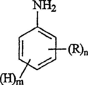
n是0-4的整数;n is an integer of 0-4;
m是1-5的整数;条件是n与m之和等于5;以及m is an integer from 1 to 5; provided that the sum of n and m is equal to 5; and
R要独立地选择,使每个出现的R都相同或不同,并要选自下列一组:烷基、链烯基、烷氧基、环烷基、环烯基、链烷醇基、烷基硫基、芳氧基、烷基硫基烷基、烷基芳基、芳基烷基、氨基、烷基氨基、二烷基氨基、芳基、烷基亚磺酰基、烷氧基烷基、烷基磺酰基、芳基硫基、芳基磺酰基、烷氧基羰基、芳基磺酰基、羧酸、卤素、氰基或被一个或多个磺酸、羧酸、卤素、硝基、氰基或环氧基取代的烷基;或羧酸、卤素、硝基、氰基、或磺酸部分;或任何2个R基一起可形成完成一个3,4,5,6或7元芳族或脂族环的亚烷基或亚链烯基链,该环可任选地包括一个或多个二价氮、硫或氧原子。无意限制本发明的范围,各种R基的大小为约1个碳原子(在烷基的情况下),经由2个或多个碳原子直到约20个碳原子,n个R的碳原子总数为约1-约40个碳原子。R is independently selected such that each occurrence of R is the same or different and is selected from the group consisting of: alkyl, alkenyl, alkoxy, cycloalkyl, cycloalkenyl, alkanol, alkyl Alkylthio, aryloxy, alkylthioalkyl, alkylaryl, arylalkyl, amino, alkylamino, dialkylamino, aryl, alkylsulfinyl, alkoxyalkyl , alkylsulfonyl, arylthio, arylsulfonyl, alkoxycarbonyl, arylsulfonyl, carboxylic acid, halogen, cyano or replaced by one or more sulfonic acid, carboxylic acid, halogen, nitro, Alkyl substituted with cyano or epoxy; or carboxylic acid, halogen, nitro, cyano, or sulfonic acid moiety; or any two R groups together can form a 3, 4, 5, 6 or 7 membered aromatic An alkylene or alkenylene chain of an aliphatic or aliphatic ring, which ring may optionally include one or more divalent nitrogen, sulfur or oxygen atoms. Without intending to limit the scope of the invention, the size of each R group is about 1 carbon atom (in the case of an alkyl group), via 2 or more carbon atoms up to about 20 carbon atoms, the total number of carbon atoms for n R from about 1 to about 40 carbon atoms.
适用于实施本发明的聚苯胺的实例是式II-V的那些:
其中,n,m和R如上所述,但因在聚合中氢原子被共价键所取代了,m要减去1以及n+m之和等于4。Among them, n, m and R are as above, but since the hydrogen atoms are replaced by covalent bonds in the polymerization, m is minus 1 and the sum of n+m is equal to 4.
y是等于或大于0的整数;y is an integer equal to or greater than 0;
x是等于或大于1的整数,条件是x与y之和要大于1;以及x is an integer equal to or greater than 1, provided that the sum of x and y is greater than 1; and
z是等于或大于1的整数。z is an integer equal to or greater than 1.
以下列出的取代和未取代苯胺是能用来制备适用于实施本发明的聚苯胺的苯胺实例。苯胺 2,5-二甲基苯胺邻-甲苯胺 2,3-二甲基苯胺间-甲苯胺 2,5-二丁基苯胺邻-乙苯胺 2,5-二甲氧基苯胺间-乙苯胺 四氢化萘胺邻-乙氧基苯胺 邻-氰基苯胺间-丁苯胺 2-硫代甲基苯胺间-己苯胺 2,5-二氯代苯胺间-辛苯胺 3-(正丁烷磺酸)苯胺4-溴代苯胺2-溴代苯胺3-溴代苯胺 2,4-二甲氧基苯胺3-乙酰胺基苯胺 4-巯基苯胺4-乙酰胺基苯胺 4-甲基硫代苯胺5-氯-2-甲氧基苯胺 3-酚氧基苯胺5-氯-2-乙氧基苯胺 4-酚氧基苯胺The substituted and unsubstituted anilines listed below are examples of anilines that can be used to prepare polyanilines suitable for use in the practice of this invention.
适用R基的实例是烷基,如甲基、乙基、辛基、壬基、叔丁基、新戊基、异丙基、仲-丁基、十二烷基等;链烯基如1-丙烯基、1-丁烯基、1-戊烯基、1-己烯基、1-庚烯基、1-辛烯基等;烷氧基如丙氧基、丁氧基、甲氧基、异丙氧基、戊氧基、壬氧基、乙氧基、辛氧基等;环烯基如环己烯基、环戊烯基等;烷醇基,如丁醇基、戊醇基、辛醇基;乙醇基、丙醇基等;烷基亚磺酰基、烷基磺酰基、烷基硫基、芳磺酰基、芳基亚磺酰基等,如丁基硫基、新戊基硫基、甲基亚磺酰基、苄基亚磺酰基、苯基亚磺酰基、丙基硫基、辛基硫基、壬基磺酰基、辛基磺酰基、甲基硫基、异丙基硫基、苯基磺酰基、甲基磺酰基、壬基硫基、苯基硫基、乙基硫基、苄基硫基、苯基(phenethyl)硫基、萘基硫基等;烷氧基羰基如甲氧基羰基、乙氧基羰基、丁氧基羰基等;环烷基如环己基、环戊基、环辛基、环庚基等;烷氧基烷基如甲氧基甲基、乙氧基甲基、丁氧基甲基、丙氧基乙基、戊氧基丁基等;芳基氧基烷基和芳基氧基芳基,如酚氧基苯基、酚氧基亚甲基等;以及各种取代烷基和芳基如1-羟基丁基、1-氨基丁基、1-羟基丙基、1-羟基戊基、1-羟基辛基、1-羟基乙基、2-硝基乙基、三氟甲基、3,4-环氧基丁基、氰基甲基、3-氯代丙基、4-硝基苯基、3-氰基苯基等;磺酸封端烷基和芳基以及羧酸封端烷基与芳基,如乙基磺酸、丙基磺酸、丁基磺酸、苯磺酸和相应的羧酸。Examples of suitable R groups are alkyl groups such as methyl, ethyl, octyl, nonyl, tert-butyl, neopentyl, isopropyl, sec-butyl, dodecyl, etc.; alkenyl groups such as 1 - propenyl, 1-butenyl, 1-pentenyl, 1-hexenyl, 1-heptenyl, 1-octenyl, etc.; alkoxy such as propoxy, butoxy, methoxy , isopropoxy, pentyloxy, nonyloxy, ethoxy, octyloxy, etc.; cycloalkenyl, such as cyclohexenyl, cyclopentenyl, etc.; alkanol, such as butanol, pentanol , octanol; ethanol, propanol, etc.; alkylsulfinyl, alkylsulfonyl, alkylthio, arylsulfonyl, arylsulfinyl, etc., such as butylthio, neopentylthio Base, methylsulfinyl, benzylsulfinyl, phenylsulfinyl, propylthio, octylthio, nonylsulfonyl, octylsulfonyl, methylthio, isopropylthio , phenylsulfonyl, methylsulfonyl, nonylthio, phenylthio, ethylthio, benzylthio, phenyl (phenethyl)thio, naphthylthio, etc.; alkoxycarbonyl such as Methoxycarbonyl, ethoxycarbonyl, butoxycarbonyl, etc.; cycloalkyl such as cyclohexyl, cyclopentyl, cyclooctyl, cycloheptyl, etc.; alkoxyalkyl such as methoxymethyl, ethoxy ylmethyl, butoxymethyl, propoxyethyl, pentoxybutyl, etc.; aryloxyalkyl and aryloxyaryl, such as phenoxyphenyl, phenoxymethylene etc.; and various substituted alkyl and aryl groups such as 1-hydroxybutyl, 1-aminobutyl, 1-hydroxypropyl, 1-hydroxypentyl, 1-hydroxyoctyl, 1-hydroxyethyl, 2- Nitroethyl, trifluoromethyl, 3,4-epoxybutyl, cyanomethyl, 3-chloropropyl, 4-nitrophenyl, 3-cyanophenyl, etc.; Alkyl and aryl terminations and carboxylic acid terminations of alkyl and aryl groups such as ethylsulfonic acid, propylsulfonic acid, butylsulfonic acid, benzenesulfonic acid and the corresponding carboxylic acids.
也适用的R基的实例有从任意2个R基团形成的二价部分,如式Examples of R groups that are also suitable are divalent moieties formed from any 2 R groups, such as the formula
-(CH2)n*--(CH 2 ) n* -
其中,n*是约3-约7的整数,例如-(CH2)4-、-(CH2)3-和-(CH2)5-,或任选地包括氧和硫等杂原子的部分,如-CH2SCH2-和-CH2-O-CH2-。适用的其它R基的实例是包括1-约3个共轭双键不饱和度的二价亚链烯基链,如二价1,3-丁二烯之类的部分。wherein n * is an integer from about 3 to about 7, such as -(CH 2 ) 4 -, -(CH 2 ) 3 - and -(CH 2 ) 5 -, or optionally including heteroatoms such as oxygen and sulfur Moieties, such as -CH 2 SCH 2 - and -CH 2 -O-CH 2 -. Examples of suitable other R groups are divalent alkenylene chains comprising from 1 to about 3 conjugated double bond unsaturations, such as divalent 1,3-butadiene or the like moieties.
优选用于本发明实施中的是以上II至V式的聚苯胺,其中:Preferred for use in the practice of the present invention are polyanilines of formulas II to V above, wherein:
n是0-约2的整数;n is an integer from 0 to about 2;
m是2-4的整数,条件是n与m之和等于4;m is an integer of 2-4, the condition is that the sum of n and m is equal to 4;
R是含1-约12个碳原子的烷基或烷氧基、氰基、卤素或被羧酸或磺酸取代基取代的烷基。R is an alkyl or alkoxy group of 1 to about 12 carbon atoms, cyano, halo or alkyl substituted with a carboxylic or sulfonic acid substituent.
x是等于或大于1的整数;x is an integer equal to or greater than 1;
y是等于或大于0的整数;条件是x与y之和大于约4,以及y is an integer equal to or greater than 0; provided that the sum of x and y is greater than approximately 4, and
z是等于或大于约5的整数。z is an integer equal to or greater than about 5.
在本发明更优选的实施方案中,聚苯胺衍生自未取代苯胺,即n为0和m为5(单体)或4(聚合物)。一般而言,单体重复单元的数目至少为约50。In a more preferred embodiment of the invention the polyaniline is derived from unsubstituted aniline, ie n is 0 and m is 5 (monomer) or 4 (polymer). Generally, the number of monomeric repeat units is at least about 50.
如美国专利5,232,631所述,聚苯胺是靠一种氧化物或酸类的存在而导电的。在该作用中,优选酸类,特别是“官能化质子酸”。“官能化质子酸”是一种反离子已优选被官能化到与该层中其它组分相容的酸。如本文所用,“质子酸”是一种把聚苯胺质子化成具有所述聚苯胺的配合物。As described in US Patent 5,232,631, polyaniline conducts electricity by the presence of an oxide or acid. In this role, acids are preferred, especially "functionalized protic acids". A "functionalized protic acid" is an acid whose counterion has preferably been functionalized to be compatible with the other components of the layer. As used herein, a "protic acid" is one that protonates polyaniline into a complex with said polyaniline.
一般而言,适用于本发明的官能化质子酸是VI和VII式所示的那些:In general, functionalized protic acids suitable for use in the present invention are those represented by formulas VI and VII:
VI A-RA-R
或 or
其中,in,
A是磺酸、硒酸、磷酸、硼酸或羧酸基;或硫酸氢盐、硒酸氢盐、磷酸氢盐;A is a sulfonic acid, selenic acid, phosphoric acid, boric acid or carboxylic acid group; or hydrogen sulfate, hydrogen selenate, hydrogen phosphate;
n是1-5的整数;n is an integer of 1-5;
R是含1-约20个碳原子的烷基、链烯基、烷氧基、链烷醇基、烷基硫基、烷基硫基烷基;或烷芳基、芳烷基、烷基亚磺酰基、烷氧基烷基、烷基磺酰基、烷氧基羰基、羧酸,其中烷基或烷氧基含0-约20个碳原子;或含3-约20个碳原子的被一个或多个磺酸、羧酸、卤素、硝基、氰基、重氮或环氧基取代的烷基;或取代或未取代的3,4,5,6或7元芳族或脂环族碳环,环上可包括1个或多个氮、硫、亚磺酰基、磺酰基或氧之类的杂原子,例如硫代苯基、吡咯基、呋喃基、吡啶基。R is alkyl, alkenyl, alkoxy, alkanol, alkylthio, alkylthioalkyl; or alkaryl, aralkyl, alkyl containing 1 to about 20 carbon atoms Sulfinyl, alkoxyalkyl, alkylsulfonyl, alkoxycarbonyl, carboxylic acid, wherein the alkyl or alkoxy group contains 0 to about 20 carbon atoms; One or more sulfonic acid, carboxylic acid, halogen, nitro, cyano, diazo or epoxy substituted alkyl groups; or substituted or unsubstituted 3, 4, 5, 6 or 7 membered aromatic or alicyclic The carbocyclic ring may contain one or more heteroatoms such as nitrogen, sulfur, sulfinyl, sulfonyl or oxygen, such as thiophenyl, pyrrolyl, furyl, pyridyl.
除上述单体酸形式之外,R还可以是一个带有许多酸官能团“A”的聚合物主链。聚合物酸的实例包括磺化聚苯乙烯、磺化聚乙烯等。在这些情况下,可选择聚合物主链以提高在非极性基体中的溶解度或溶于在其中可以用聚合物、聚丙烯酸或聚乙烯基磺酸酯等材料的极性更强的基体中。In addition to the monomeric acid forms described above, R can also be a polymer backbone with a plurality of acid functional groups "A". Examples of polymeric acids include sulfonated polystyrene, sulfonated polyethylene, and the like. In these cases, the polymer backbone can be chosen to increase solubility in non-polar matrices or in more polar matrices where materials such as polymers, polyacrylic acid, or polyvinyl sulfonate can be used .
R′在每次出现时都相同或不同,且是烷基、链烯基、烷氧基、环烷基、环烯基、链烷醇基、烷基硫基、芳氧基、烷基硫基烷基、烷基芳基、芳基烷基、烷基亚磺酰基、烷氧基烷基、烷基磺酰基、芳基、芳基硫基、芳基suldmyl、烷氧基羰基、芳基磺酰基、羧酸、卤素、氰基或被一个或多个磺酸、羧酸、卤素、硝基、氰基、重氮或环氧基取代的烷基;或任意2个R取代基在一起是完成一个3,4,5,6或7元芳族或脂环族碳环或它们倍数的亚烷基或亚链烯基,这样一个或多个环上可包括一个或多个氮、硫、sulEmyl、磺酰基或氧之类的二价杂原子。R′一般有约1-约20个碳原子,尤其3-20个,更尤其约8-20个碳原子。R' is the same or different in each occurrence and is alkyl, alkenyl, alkoxy, cycloalkyl, cycloalkenyl, alkanolyl, alkylthio, aryloxy, alkylthio alkylalkyl, alkylaryl, arylalkyl, alkylsulfinyl, alkoxyalkyl, alkylsulfonyl, aryl, arylthio, aryl suldmyl, alkoxycarbonyl, aryl Sulfonyl, carboxylic acid, halogen, cyano, or alkyl substituted by one or more sulfonic acid, carboxylic acid, halogen, nitro, cyano, diazo, or epoxy; or any 2 R substituents together It is an alkylene or alkenylene group that completes a 3, 4, 5, 6 or 7-membered aromatic or alicyclic carbocyclic ring or multiples thereof, such that one or more rings may include one or more nitrogen, sulfur , sulEmyl, sulfonyl or divalent heteroatoms such as oxygen. R' generally has about 1 to about 20 carbon atoms, especially 3 to 20, more especially about 8 to 20 carbon atoms.
优选以上VI与VII式的材料,其中Materials of formulas VI and VII above are preferred, wherein
A是磺酸、磷酸或羧酸;A is sulfonic acid, phosphoric acid or carboxylic acid;
n是1-3的整数;n is an integer of 1-3;
R是含6-约14个碳原子的烷基、链烯基、烷氧基;或烷基或烷基部分或烷氧基有4-约14个碳原子的芳烷基;或有6-约14个碳原子的被一个或多个羧酸、卤素、重氮或环氧基取代的烷基。R is an alkyl, alkenyl, alkoxy group containing 6 to about 14 carbon atoms; or an aralkyl group with 4 to about 14 carbon atoms in an alkyl or alkyl moiety or alkoxy group; or 6- An alkyl group of about 14 carbon atoms substituted with one or more carboxylic acid, halogen, diazo or epoxy groups.
R′每次出现都相同或不同,而且是含4-14个碳原子的烷基、烷氧基、烷基磺酰基或被一个或多个卤素部分取代的烷基,烷基部分也有4-14个碳原子。Each occurrence of R' is the same or different, and is alkyl, alkoxy, alkylsulfonyl or alkyl substituted by one or more halogen moieties containing 4-14 carbon atoms, and the alkyl moiety also has 4- 14 carbon atoms.
在特别优选的实施方案中,非常优选用于实施本发明的是以上VI和VII式的官能化质子酸,其中In a particularly preferred embodiment, very preferred for the practice of the present invention are the functionalized protonic acids of the formulas VI and VII above, wherein
A是磺酸;A is sulfonic acid;
n是1或2的整数;n is an integer of 1 or 2;
R是含6-约14个碳原子的烷基或烷氧基;或含6-约14个碳原子的被一个或多个卤素取代的烷基。R is an alkyl or alkoxy group of 6 to about 14 carbon atoms; or an alkyl group of 6 to about 14 carbon atoms substituted with one or more halogens.
R′是含4-14个碳原子,尤其12个碳原子的烷基或烷氧基,或被一个或多个卤素取代的烷基。R' is an alkyl or alkoxy group containing 4-14 carbon atoms, especially 12 carbon atoms, or an alkyl group substituted by one or more halogens.
优选的官能化质子酸是有机磺酸,如十二烷基苯磺酸,更优选聚(2-芳基酰氨基-2-甲基-1-丙烷磺酸)(“PAAMPSA”)。Preferred functionalized protic acids are organic sulfonic acids, such as dodecylbenzenesulfonic acid, more preferably poly(2-arylamido-2-methyl-1-propanesulfonic acid) ("PAAMPSA").
官能化质子酸的用量可根据所需的电导率而变。一般而言,要将官能化程度足够高的质子酸加入含聚苯胺的混合物中以形成一种导电材料。通常官能化质子酸的用量至少要足以得到一种导电聚合物(以溶液形式或固体形式)。The amount of functionalized protic acid can vary depending on the desired conductivity. In general, a protic acid sufficiently functionalized is added to the polyaniline-containing mixture to form a conductive material. Usually the functionalized protic acid is used in an amount at least sufficient to obtain a conductive polymer (either in solution or solid form).
聚苯胺可以任何物理形式方便地用于本发明实施中。适用形式的实例是在Green,A.G.,和Woodhead,A.E.,J.Chem.Soc.,101,1117(1912)和Kobay.ashi等,J.Electroanl.Chem.,177,281-91(1984)中所述的那些,这些参考文献包括于此供参考。对于未取代聚苯胺,有用的形式包括无色翠绿亚胺、质子翠绿亚胺、翠绿亚胺、苯胺黑和甲苯-质子翠绿亚胺形式,优选翠绿亚胺形式。The polyaniline may be conveniently used in the practice of the present invention in any physical form. Examples of suitable forms are in Green, A.G., and Woodhead, A.E., J. Chem. Soc., 101, 1117 (1912) and Kobay.ashi et al., J. Electroanl. Chem., 177, 281-91 (1984) Those references are incorporated herein by reference. For unsubstituted polyaniline, useful forms include leuco emeraldine, protic emeraldine, emeraldine, nigrosine, and toluene-protic emeraldine forms, with emeraldine forms being preferred.
Cao,Y和Zhang,C.的未决PCT专利申请PCT/US00/32545公开了共轭聚合物与非导电聚合物的低电导率共混物的形成,包括于此供参考。Pending PCT patent application PCT/US00/32545 by Cao, Y. and Zhang, C. discloses the formation of low conductivity blends of conjugated polymers and nonconductive polymers, and is incorporated herein by reference.
加入共轭聚合物的一种或多种具体的本体聚合物可以改变。材料的选择可以基于导电聚合物的性质、用来共混聚合物的方法和用来在器件上沉积薄层的方法。The particular bulk polymer(s) added to the conjugated polymer can vary. The choice of material can be based on the properties of the conducting polymer, the method used to blend the polymers and the method used to deposit the thin layer on the device.
材料共混的方法可以是将一种聚合物分散在另一种聚合物中,作为细颗粒分散体系或一种聚合物在另一种聚合物中的溶液。聚合物一般以液相混合,而薄层一般由液相铺敷而成。Materials can be blended by dispersing one polymer in another, as a fine particle dispersion or as a solution of one polymer in another. Polymers are generally mixed in the liquid phase, and thin layers are generally laid down from the liquid phase.
我们用水溶性或水分散性共轭聚合物与水溶性或水分散性本体聚合物已得到了最好的结果。在这种情况下,共混物可以通过将两种聚合物溶解或分散在水中,然后从溶液或分散体浇注成层。We have had the best results with water soluble or water dispersible conjugated polymers and water soluble or water dispersible bulk polymers. In this case, the blend can be formed by dissolving or dispersing the two polymers in water and then casting the layer from the solution or dispersion.
有机溶剂可以与有机-可溶或有机可分散共轭聚合物和本体聚合物一起使用。此外,共混物可以用两种聚合物的熔体形成,或用一种液态预聚体或本体聚合物的单体形式形成,然后使之聚合或固化成所需的最终材料。Organic solvents can be used with organo-soluble or organodispersible conjugated polymers and bulk polymers. In addition, blends can be formed from the melt of the two polymers, or from a liquid prepolymer or the monomeric form of the bulk polymer, which is then allowed to polymerize or cure into the desired final material.
在目前优选的PANI是水溶性或水分散性的且希望从含水溶液浇注PANI层的情况下,本体聚合物应该是水溶性或水分散性的。在这类情况下,要选自,例如,聚芳基酰胺(PAM)、聚(丙烯酸)、(PAA)聚(乙烯基吡咯烷酮)(PVPd)、丙烯酰胺共聚物、纤维素衍生物、羧基乙烯基聚合物、聚乙二醇、聚环氧乙烷(PEO)、聚乙烯醇(PVA)、聚乙烯基甲醚、聚胺、聚亚胺、聚乙烯基吡啶、多糖及聚氨酯分散体。In cases where the presently preferred PANI is water soluble or water dispersible and it is desired to cast the PANI layer from an aqueous solution, the bulk polymer should be water soluble or water dispersible. In such cases, it is selected from, for example, polyarylamides (PAM), poly(acrylic acid), (PAA) poly(vinylpyrrolidone) (PVPd), acrylamide copolymers, cellulose derivatives, carboxyvinyl Polymers, Polyethylene Glycol, Polyethylene Oxide (PEO), Polyvinyl Alcohol (PVA), Polyvinyl Methyl Ether, Polyamine, Polyimine, Polyvinylpyridine, Polysaccharides and Polyurethane Dispersions.
在要求从非水溶液或非水分散体浇注薄层的情况下,本体聚合物可选自,例如,可液化聚乙烯、全同立构聚丙烯、聚苯乙烯、聚乙烯醇、聚乙基乙烯基醋酸酯、聚丁二烯、聚异戊二烯、乙烯亚乙烯基共聚物、乙烯-丙烯共聚物、聚对苯二甲酸乙二酯、聚对苯二甲酸丁二酯以及尼龙,如尼龙12、尼龙8、尼龙6、尼龙6.6等,聚酯材料、聚酰胺如聚丙烯酰胺等。Where casting of thin layers from non-aqueous solutions or non-aqueous dispersions is required, the bulk polymer may be selected from, for example, liquefiable polyethylene, isotactic polypropylene, polystyrene, polyvinyl alcohol, polyethylene vinyl Acetate, polybutadiene, polyisoprene, ethylene vinylidene copolymer, ethylene-propylene copolymer, polyethylene terephthalate, polybutylene terephthalate, and nylon, such as
在要将一种聚合物分散在另一种中的那些情况下,可不要求各聚合物的共同溶解度。In those cases where one polymer is to be dispersed in another, common solubility of the individual polymers may not be required.
聚苯胺与本体聚合物或预聚体的相对比例可以改变。对于每一份聚苯胺,可以配0-多达20重量份的本体聚合物或预聚物,从而对于每份PANI存在0.5-10份,尤其1-4份本体材料。The relative proportions of polyaniline to bulk polymer or prepolymer can vary. From 0 to up to 20 parts by weight of bulk polymer or prepolymer can be formulated for each part of polyaniline so that there are 0.5 to 10 parts, especially 1 to 4 parts of bulk material for each part of PANI.
选择浇注该薄层所要用的溶剂,以适应聚合物的性能。The solvent to be used to cast the thin layer is chosen to suit the properties of the polymer.
在优选体系中,PANI和本体聚合物都是水溶性或水分散性的,以及溶剂体系是含水溶剂体系,如水或水与一种或多种极性有机材料如低级醇、酮和酯等低级含氧烃的混合物。In a preferred system, both the PANI and the bulk polymer are water-soluble or water-dispersible, and the solvent system is an aqueous solvent system, such as water or water with one or more polar organic materials such as lower alcohols, ketones, and esters. Mixture of oxygenated hydrocarbons.
这些材料包括,但不限于,水与甲醇、乙醇、异丙醇、丙酮、甲乙酮等的混合物。These materials include, but are not limited to, mixtures of water with methanol, ethanol, isopropanol, acetone, methyl ethyl ketone, and the like.
如果需要,但一般不优选,可以用极性有机液体的溶剂体系。If desired, but generally not preferred, solvent systems of polar organic liquids can be used.
在导电聚合物如PANI与本体聚合物不溶于水或不可水分散的情况下,最常用非极性溶剂。Non-polar solvents are most commonly used in the case of conductive polymers such as PANI and bulk polymers that are insoluble or non-dispersible in water.
适用的普通非极性溶剂的实例有下述材料:取代或未取代的芳族烃,如苯、甲苯、对-二甲苯、间-二甲苯、萘、乙苯、苯乙烯、苯胺等;高级烷烃,如戊烷、己烷、庚烷、辛烷、壬烷、癸烷等;环烷烃,如十氢化萘;卤代烷烃如氯仿、溴仿、二氯甲烷等;卤代芳烃,如氯代苯、邻-二氯代苯、间-二氯代苯、对二氯代苯等;高级醇如2-丁醇、1-丁醇、己醇、戊醇、癸醇、2-甲基-1-丙醇等;高级酮如己酮、丁酮、戊酮等;杂环如吗啉;全氟代烃如全氟代萘烷、全氟代苯等。Examples of suitable common non-polar solvents include the following materials: substituted or unsubstituted aromatic hydrocarbons such as benzene, toluene, p-xylene, m-xylene, naphthalene, ethylbenzene, styrene, aniline, etc.; Alkanes, such as pentane, hexane, heptane, octane, nonane, decane, etc.; cycloalkanes, such as decalin; halogenated alkanes, such as chloroform, bromoform, methylene chloride, etc.; halogenated aromatics, such as chlorinated Benzene, o-dichlorobenzene, m-dichlorobenzene, p-dichlorobenzene, etc.; higher alcohols such as 2-butanol, 1-butanol, hexanol, pentanol, decanol, 2-methyl- 1-propanol, etc.; higher ketones such as hexanone, butanone, pentanone, etc.; heterocycles such as morpholine; perfluorohydrocarbons such as perfluorodecalin, perfluorobenzene, etc.
第二层112的厚度将根据二极管的性能选择。在复合阳极要透明的情况下,考虑到图1所示的失效问题,一般优选PANI层在实践允许范围内尽可能薄。典型厚度范围为约100-约5000。当要求透明度时,优选厚度约100-约3000,尤其约2000。The thickness of the
当第二层112包含一种PANI(ES)共混物且膜厚为200nm或更厚时,第二层的电阻率应大于或等于104Ω-cm,以免串扰和象素间漏电。优选大于105Ω-cm的值。即使在105Ω-cm,仍会有些残余漏电,因此器件效率有些下降。因此更优选约105-108Ω-cm的值。大于109的值将导致注入/缓冲层厚度方向上明显的压降,因此应避免。高电导率第三层(114) When the
要选择用于第三层114的材料以匹配光活性层102的能级,或提高多层阳极104的空穴注入/输运能力,或提高多层阳极104与光活性层102之间界面上的界面性能。The material for the
空穴-注入电极这个第三部件是一层很薄的高导电有机聚合物,其电阻低于第二层112材料的电阻而高于第一层110的电阻。一种典型的导电有机聚合物包括高导电形式的纯PANI、聚吡咯,优选聚噻吩,如PEDT,以及在前节关于第二层112中所述的任何其它材料。The hole-injecting electrode This third component is a thin layer of highly conductive organic polymer with a resistance lower than that of the material of the
形成层(114)的材料的体积电导率应是第二层(112)体积电导率的约5倍-约106倍。同样,体积电阻率应低5-106倍。要求多层阳极104透明且该层包含PEDT时,第三层一般非常薄,常常薄到几乎形不成一个完整的连续层。厚度应在约5-约500范围内,一般优选10-50。The bulk conductivity of the material forming layer (114) should be from about 5 times to about 106 times the bulk conductivity of the second layer (112). Likewise, the volume resistivity should be 5-10 times lower. Where
在第二层上加上高电导率第三层(114)就产生一个多层结构,其电导高于单独第二层时观察到的值。该双层(112与114)结构的电导与单独第二层112的电导之比应在1.25-20范围内,优选1.5-15,尤其优选2-10。阴极(106) The addition of a high conductivity third layer (114) on top of the second layer results in a multilayer structure with higher conductance than that observed with the second layer alone. The ratio of the conductance of the bilayer (112 and 114) structure to the conductance of the
适用于作阴极材料的材料是功函低于第一电接触层(在此情况下,是阳极)的任何金属或非金属。用于阴极层106的材料(在此情况下是第二电接触层)可选自族1的碱金属(如Li,Cs);族2的碱土金属——一般是钙、钡、锶;族12的金属;稀土金属——一般是钇、镧系和锕系。也能用铝、铟和铜、银、它们的结合以及与钙和/或钡、Li、镁、LiF结合等的材料。低功函金属的合金,如镁在银中和锂在铝中的合金也有用。Materials suitable for use as cathode material are any metal or non-metal having a lower work function than the first electrical contact layer (in this case, the anode). The material for the cathode layer 106 (in this case the second electrical contact layer) may be selected from group 1 alkali metals (eg Li, Cs);
电子-注入阴极层的厚度范围是从小于15至多达5,000之厚。阴极层106可以图形化以给出一个象素化阵列,也可以是连续的并与一层本身已图形化的主体导体如银、铜或优选铝重叠。The thickness of the electron-injecting cathode layer ranges from less than 15 Å to as much as 5,000 Å thick.
阴极层还可包括一层为给出力学强度与耐久性而加入的第二金属的第二层。衬底(108) The cathode layer may also include a second layer of a second metal added to give mechanical strength and durability. Substrate(108)
在大多数实施方案中,是在衬底上制造二极管。一般地说,衬底应是非导电的。在透光的实施方案中,它是透明的。衬底可以是一种刚性材料,如刚性塑料,包括刚性丙烯酸酯、聚碳酸酯等,刚性无机氧化物如玻璃、石英、蓝宝石等。也可以是一种柔性透明有机聚合物,如聚酯——例如聚对苯二甲酸乙二酯、柔性聚碳酸酯、聚甲基丙烯酸甲酯、聚苯乙烯等。In most embodiments, the diodes are fabricated on a substrate. In general, the substrate should be non-conductive. In light transmissive embodiments, it is transparent. The substrate can be a rigid material such as rigid plastics including rigid acrylics, polycarbonates, etc., rigid inorganic oxides such as glass, quartz, sapphire, etc. It may also be a flexible transparent organic polymer such as polyester - eg polyethylene terephthalate, flexible polycarbonate, polymethyl methacrylate, polystyrene, etc.
衬底的厚度并不太重要。接触垫片(80,82) The thickness of the substrate is not too critical. Contact pads (80, 82)
任何适用于将器件100的电极连接到电源(未示出)的接触垫片80,82都可用,包括,例如,导电金属如金(Au)、银(Ag)、镍(Ni)、铜(Cu)或铝(Al)。Any
优选接触垫片80,82的高度(未示出)超出高功函电极线110的厚度,后者低于层的总厚度。Preferably the height (not shown) of the
优选层102、110和112的尺寸使接触垫片80位于衬底上一个未被102、112和114所复盖的部分。此外,层106、102、110和112的尺寸要使电极线106和电极线110的整个长度与宽度上有至少一层102、112插在电极106、110之间,而电连接可制在电极106与接触垫片80之间。其它任选层
在光活性层102与阴极106之间可以有一层包括电子注入/输运材料的任选层。该任选层能同时有利于电子注入/输运,并起防止在层界面上发生淬火反应的缓冲层或约束层的作用。优选该层促进电子的活动能力并减少淬火反应。用于任选层140的电子输运材料的实例包括金属螯合氧化型化合物,例如三(8-羟基醌酯基)铝(Alq3);菲咯啉-基化合物,如2,9-二甲基-4,7-二苯基-1,10-菲咯啉(DDPA)或4,7-二苯基-1,10-菲咯啉(DPA),以及吡咯化合物如2-(4-二苯基)-5-(4-叔丁基苯基)-1,3,4-噁二唑(PBD)和3-(4-二苯基)-4-苯基-5-(4-叔丁基苯基)-1,2,4-三唑(TAZ)、含DIPA、DPA、PBD和TAZ部分的聚合物及它们的共混物;含DDPA、DPA、PBD和TAZ的聚合物共混物。Between the
阳极层110、112、114、光活性层102和阴极层106中的部分或全部都可以经表面处理以提高载流子输运效率。每一元件层材料的选择优选通过平衡提供一个高效器件这一目标来决定。制造技术 Some or all of the anode layers 110, 112, 114,
本发明器件的各种元件可以用本领域内熟知的任何技术来制造,例如溶液浇注、丝网印刷、料卷涂布、喷墨印刷、溅涂、蒸涂、前体聚合物加工、熔体加工等,或它们的任何组合。The various elements of the device of the present invention can be fabricated by any technique well known in the art, such as solution casting, screen printing, web coating, inkjet printing, sputtering, vapor coating, precursor polymer processing, melt processing, etc., or any combination thereof.
在最常用的方法中,制造二极管的方法是,在衬底上依次沉积各层。在一种典型的制造方法中,首先铺敷复合电极104中导电的第一层110。沉积该层的方法一般是真空溅涂(RF或Magnetron)、电子束蒸发、热蒸气沉积、化学蒸积或常用来形成无机层的类似方法。In the most common method, diodes are fabricated by sequentially depositing layers on a substrate. In a typical manufacturing method, the conductive
接着,铺敷低电导率第二层112。该层常常很方便地由旋转浇注或类似技术沉积自溶液。在由水溶性或水分散性材料形成该层的优选情况下,一般用水作为旋转浇注介质。在要求非水溶剂的情况下,要用甲苯、二甲苯、苯乙烯、苯胺、十氢萘、氯仿、二氯甲烷、氯代苯和吗啉等。该层可以如一般入档的美国临时专利申请60/212,934中所述进行热处理。Next, a low-
然后,沉积较高电导率层114。这一步一般也从溶液形成,溶剂按有关层112沉积的参考文献所述进行选择。Then, a
然后,沉积共轭聚合物的光活性层102。共轭聚合物能直接从溶液沉积或浇注。所用的溶剂是要溶解该聚合物而不会干扰其后续沉积的一种溶剂。Then, a
一般用有机溶剂。这类溶剂可包括卤代烃,如二氯甲烷、氯仿和四氯化碳,芳烃如二甲苯、苯、甲苯,其它烃如十氢化萘等。也可以用混合溶剂。极性溶剂如水、丙酮、酸等也适用。这些只不过是代表性举例,溶剂可以广泛选自满足上述准则的许多材料。Usually organic solvents are used. Such solvents may include halogenated hydrocarbons such as methylene chloride, chloroform, and carbon tetrachloride, aromatic hydrocarbons such as xylene, benzene, toluene, other hydrocarbons such as decahydronaphthalene, and the like. Mixed solvents can also be used. Polar solvents such as water, acetone, acids, etc. are also suitable. These are merely representative examples, and the solvent can be selected from a wide range of materials satisfying the above criteria.
当在衬底上沉积各种聚合物时,溶液应比较稀,例如浓度为0.1-20重量%,尤其0.2-5重量%。膜厚一般用500-4000,尤其1000-2000。When depositing various polymers on the substrate, the solution should be relatively dilute, for example, the concentration is 0.1-20% by weight, especially 0.2-5% by weight. The film thickness is generally 500 Å-4000 Å, especially 1000 Å-2000 Å.
最后,要加上低功函电子-注入接触。这种接触一般由真空蒸发在活性聚合物层表面上。Finally, low work function electron-injection contacts are added. This contacting is generally by vacuum evaporation on the surface of the active polymer layer.
上述步骤可以改变甚至逆转,如果需要“倒置二极管”。The above steps can be changed or even reversed, if desired to "invert the diode".
应该理解,上述结构及它们的制造方法可加以改变以包括赋予物理强度和保护的其它层,以改变发射光的颜色或二极管的灵敏度等。进一步还应理解,本发明还适用于有机电子器件,包括本发明中不含光活性层的多层阳极在内,例如,晶体管、电容器、电阻器、化学电阻传感器(气体/蒸气敏感电子探头,化学和生物传感器)、写入传感器和电致变色传感器(智能窗)。It should be understood that the structures described above and their methods of fabrication may be modified to include other layers that impart physical strength and protection, to change the color of emitted light or the sensitivity of the diodes, and the like. It should further be understood that the present invention is also applicable to organic electronic devices, including multilayer anodes of the present invention that do not contain a photoactive layer, such as transistors, capacitors, resistors, chemical resistance sensors (gas/vapor sensitive electronic probes, chemical and biological sensors), write sensors and electrochromic sensors (smart windows).
本发明将通过下述实施例作进一步描述,给出这些实施例是为了解释本发明而无意限制本发明的范围。The present invention will be further described by the following examples, which are given for the purpose of illustration of the invention and are not intended to limit the scope of the invention.
实施例1 Example 1
PANI(ES)按以下参考文献制备(Y.Cao等,Polymer,30(1989)2307)。翠绿亚胺盐(ES)形式由典型的绿色证实。用聚(2-丙烯氨基-2-甲基-1-丙烷磺酸(PAAMPSA)(Aldrich)代替参考文献中的HCl。首先,在30.5g(0.022mol)浓度为15%的PAAMPSA水溶液(Aldrich)中加进170ml水,使之稀释到2.3%。边搅拌边在PAAMPSA溶液中加入2.2g(0.022M)苯胺。然后在剧烈搅拌中,向苯胺/PAAMPSA溶液中慢慢加入2.01g(0.0088M)在10ml水中的过硫酸铵。反应混合物在室温下搅拌24小时。为沉淀出产物PANI(ES),在反应混合物中加入1000ml丙酮。滗出大部分丙酮/水,然后过滤PANI(ES)沉淀物。用丙酮清洗所得的胶状产物数次,然后在40℃动态真空下干燥24小时。PANI(ES) was prepared according to the following reference (Y. Cao et al., Polymer, 30(1989) 2307). The emeraldine salt (ES) form is evidenced by a typical green color. Poly(2-propenylamino-2-methyl-1-propanesulfonic acid (PAAMPSA) (Aldrich) was used to replace HCl in the reference. First, in 30.5 g (0.022 mol) of 15% aqueous solution of PAAMPSA (Aldrich) Add 170ml of water to make it diluted to 2.3%. While stirring, add 2.2g (0.022M) aniline in the PAAMPSA solution. Then in vigorous stirring, slowly add 2.01g (0.0088M) in the aniline/PAAMPSA solution Ammonium persulfate in 10 ml of water. The reaction mixture was stirred at room temperature for 24 hours. To precipitate out the product PANI(ES), 1000 ml of acetone was added to the reaction mixture. Most of the acetone/water was decanted and the PANI(ES) precipitate was filtered The resulting gummy product was washed several times with acetone and then dried at 40°C under dynamic vacuum for 24 hours.
该实施例示意了PANI(ES)的直接合成。This example illustrates the direct synthesis of PANI(ES).
实施例2 Example 2
将4g实施例1中制得的PANI(ES)粉末与400g去离子水在一个塑料瓶内混合。在室温下旋转该混合物48小时。然后将该溶液/分散体滤过1μm聚丙烯漏斗。按例行程序,通过改变混合在水中的PANI(ES)量制备不同浓度的PANI(ES)水溶液。4g of PANI(ES) powder prepared in Example 1 was mixed with 400g of deionized water in a plastic bottle. The mixture was rotated at room temperature for 48 hours. The solution/dispersion was then filtered through a 1 μm polypropylene funnel. PANI(ES) aqueous solutions with different concentrations were prepared by changing the amount of PANI(ES) mixed in water as a routine procedure.
该实施例表明PANI(ES)可以溶于/分散于水中并接着滤过1μm漏斗。This example shows that PANI(ES) can be dissolved/dispersed in water and then filtered through a 1 μm funnel.
实施例3 Example 3
用等量的去离子水稀释聚亚乙二氧基噻吩PEDT(Baytron P.专用级,购自Bayer)溶液。在室温下搅拌该溶液过夜。溶液中的PEDT含量为0.8%。也制备PEDT含量分别为0.4、0.2和0.16%的PEDT溶液。所有这些溶液都能滤过0.231μm漏斗。Dilute polyethylenedioxythiophene PEDT (Baytron P. special grade, purchased from Bayer) solution with an equal amount of deionized water. The solution was stirred overnight at room temperature. The PEDT content in the solution was 0.8%. PEDT solutions with PEDT contents of 0.4, 0.2 and 0.16%, respectively, were also prepared. All of these solutions were able to filter through 0.231 μm funnels.
实施例4 Example 4
将30g实施例2中制得的PANI(ES)与7g去离子水和0.6g聚芳基酰胺(PAM)(M.W.5,000,000-6,000,000,Polysciences)在室温下搅拌混合4-5天。在共混物溶液中PANI(ES)与PAM的重量比为1∶2。还制备了PANI(ES)与PAM的重量比分别为1∶1、1∶1.5、1∶2.5、1∶3、1∶4、1∶5、1∶6和1∶9的共混物溶液。30 g of PANI (ES) prepared in Example 2, 7 g of deionized water and 0.6 g of polyarylamide (PAM) (M.W. 5,000,000-6,000,000, Polysciences) were stirred and mixed at room temperature for 4-5 days. The weight ratio of PANI(ES) to PAM in the blend solution is 1:2. Blend solutions with weight ratios of PANI(ES) to PAM of 1:1, 1:1.5, 1:2.5, 1:3, 1:4, 1:5, 1:6 and 1:9 were also prepared .
实施例5 Example 5
制备带图形化ITO电极的玻璃衬底。用实施例2,3和4中制备的PANI、PEDT和PANI共混物溶液,在图形化衬底上表面旋转浇注各层,然后在真空烘箱内于90℃焙烘0.5小时。然后薄膜在烘箱内于200℃下处理30分钟。用高阻静电计测量ITO电极间的电阻。用Dec-Tac表面仿形仪(Alpha-Step 500表面仿形仪,Tencor Instrument)测量膜厚。表1比较了PANI(ES)、PANI(ES)-PAM共混物和PEDT膜的电导率与厚度。如由表可见,PANI(ES)和PEDT的电导率分别为10-4和10-3S/cm。两个值都太高,不适用于象素化显示器。经高温处理过的PANI(ES)-PAM共混物,具有这些材料用于象素化显示器的理想电导率和厚度。Prepare glass substrates with patterned ITO electrodes. Using the PANI, PEDT and PANI blend solutions prepared in Examples 2, 3 and 4, the layers were spin-cast on the surface of the patterned substrate, and then baked in a vacuum oven at 90° C. for 0.5 hour. The films were then oven-conditioned at 200°C for 30 minutes. The resistance between the ITO electrodes was measured with a high-resistance electrometer. Film thickness was measured with a Dec-Tac Surface Profiler (Alpha-
本实施例说明,经高温处理过的PANI(ES)共混物具有适用于象素化显示器的理想电导率和厚度;即无需图形化PANI(ES)共混膜,象素间的漏电就能被限制到足够低。This embodiment illustrates that the PANI (ES) blend that has been processed at high temperature has ideal conductivity and thickness suitable for pixelated displays; is limited sufficiently low.
表1:PANI(ES)、PANI(ES)-PAM共混物和PEDT的体积电导率Table 1: Bulk conductivity of PANI(ES), PANI(ES)-PAM blends and PEDT
共混物 焙烘条件 厚度() 电导率(S/cm)Blend Baking Conditions Thickness () Conductivity (S/cm)
PANi ---------- 426 5.1×10⁻⁴ PANi ---------- 426 5.1×10 -4
PEDT ---------- 1221 1.8×10⁻³ PEDT ---------- 1221 1.8×10 -3
PANi-PAM(1∶2) 200℃/30min 2195 7.4×10⁻⁷ PANi-PAM(1:2) 200℃/30min 2195 7.4×10 -7
实施例6 Example 6
用可溶性聚(1,4-亚苯基亚乙烯基)共混物(C-PPV)(H.Becker,H.Spreitzer,W.Kreduer,E.K1uge,H.Schenk,I.D.Parker和Y.Cao,AdV.Mater.12,42(2000)作为活性半导体发光聚合物制造发光二极管;C-PPV膜的厚度是700-900。C-PPV发射黄-绿光,发光峰在~560nm。用铟/锡氧化物作阳极接触层。然后用实施例2,3和4中制备的溶液涂布PANI、PEDT或PANI-PAM共混物层。这些层在图形化衬底表面上旋转浇注而成。这些层在真空烘箱内于90℃焙烘30分钟,然后在烘箱内于200℃处理30分钟。加上活性层和一个金属阴极。该器件的结构是ITO/聚苯胺共混物/C-PPV/金属。用ITO在玻璃上(Applied ITO/玻璃)和ITO在聚对苯二甲酸乙二酯PET塑料上作为衬底(Courtauld公司的ITO/PET)制造器件;在两种情况下,ITO/聚苯胺共混物双层是阳极和空穴-注入接触。以一层Ca或Ba作为阴极制造器件。用真空蒸气沉积法在低于1×10-6乇的压力下在C-PPV层表面上制造金属阴极膜,形成一个面积为3cm2的活性层。沉积用STM-100厚度/速率计(Sycon Instruments公司)监控。在15钡层上沉积2,000-5,000铝。对于每一器件,测量电流-电压曲线,光-电压曲线以及量子效率。对具有不同共混物层的器件测得的工作电压和效率概括在表2中。正如由这些数据可见,最低的工作电压和最高的光输出由含PEDT层的器件实现了。With soluble poly(1,4-phenylene vinylene) blends (C-PPV) (H.Becker, H.Spreitzer, W.Kreduer, E.Kluge, H.Schenk, ID Parker and Y.Cao, AdV.Mater.12,42(2000) manufacture light-emitting diode as active semiconducting light-emitting polymer; The thickness of C-PPV film is 700-900 Å.C-PPV emits yellow-green light, and luminescence peak is at~560nm.Use indium/ Tin oxide is used as the anode contact layer. Then with
本实施例说明性能最佳的聚合物LED能用PEDT作为空穴注入(缓冲)层制成。This example demonstrates that the best performing polymer LEDs can be made with PEDT as the hole injection (buffer) layer.
表2用PANI(ES)、PANI(ES)-PAM共混物和PEDT制成器件的性能Table 2 Properties of devices made of PANI(ES), PANI(ES)-PAM blends and PEDT
共混物 焙烘条件 器件在8.3mA/cm2下的性能Blend Baking Condition Device Performance at 8.3mA/cm 2
V cd/A Lm/WV cd/A Lm/W
PANi --------- 4.7 7.4 4.9PANi --------- 4.7 7.4 4.9
PEDT --------- 4.5 7.7 5.2PEDT --------- 4.5 7.7 5.2
PANi-PAM(1∶2) 200℃/30min 6.6 7.2 3.6PANi-PAM(1∶2) 200℃/30min 6.6 7.2 3.6
实施例7 Example 7
用一块夹在紫外光固化环氧间的盖玻片封装按实施例6生产的器件。在烘箱内于70℃的温度下,在该封装器件中通以3.3mA/cm2的恒定电流。通过器件的总电流是10mA,发光强度为200烛光/cm2。表3和图3示意在70℃下工作期间的光输出和电压上升。在图3中用虚线分别示出器件300、302和304的光输出300-1、302-1和304-1。在图3中用实线分别示出器件300、302和304的电压输出300-2、302-2和304-2。The device produced in Example 6 was encapsulated with a cover glass sandwiched between UV-cured epoxy. A constant current of 3.3 mA/cm 2 was passed through the packaged device at a temperature of 70° C. in an oven. The total current through the device was 10 mA and the luminous intensity was 200 cd/cm 2 . Table 3 and Figure 3 illustrate the light output and voltage rise during operation at 70°C. Light outputs 300-1, 302-1, and 304-1 of
与以PANI(ES)和PANI(ES)-PAM共混物作阳极的器件在70℃应力作用下于160-190小时内降解相反,具有PEDT层的器件的半寿命达到300小时,伴随着一个非低的升压(4.3mV/小时)。其寿命差不多比具有PANI(ES)-PAM共混物的器件长2倍。但仅有PEDT层的电阻还不够高,不足以避免象素间的漏电,因而不适用于象素化显示器。从在50℃、70℃和85℃采集的光亮度衰减和电压上升数据的Ahrennius曲线,估计在70℃下温度加速因子约为25。因此对于具有PEDT层的器件,确定在室温下的外推应力寿命约为7,500小时。In contrast to the degradation of devices with PANI(ES) and PANI(ES)-PAM blends as anodes under stress at 70 °C within 160–190 h, the half-life of devices with PEDT layers reached 300 h, accompanied by a Non-low boost (4.3mV/hour). Its lifetime is almost 2 times longer than the device with PANI(ES)-PAM blend. However, the resistance of the PEDT layer alone is not high enough to avoid leakage between pixels, so it is not suitable for pixelated displays. From the Ahrennius curves of luminance decay and voltage rise data collected at 50°C, 70°C, and 85°C, a temperature acceleration factor of about 25 was estimated at 70°C. The extrapolated stress lifetime at room temperature was thus determined to be approximately 7,500 hours for a device with a PEDT layer.
该实施例说明最长的寿命能从由PEDT层制成的聚合物LED获得。但是,这些层的电阻不够高,不足以避免象素间的漏电。表3:用PANI(ES)、PANI(ES)-PAM共混物和PEDT制造的LED器件的应力寿命This example illustrates that the longest lifetime can be obtained from polymer LEDs made from PEDT layers. However, the resistance of these layers is not high enough to avoid leakage between pixels. Table 3: Stress lifetime of LED devices fabricated with PANI(ES), PANI(ES)-PAM blends, and PEDT
图3 共混物 焙烘条件 在70℃3.3mA/cm2下的应力寿命Fig.3 Stress life of blends baked at 70℃3.3mA/ cm2
参考号Reference No
mV/h cd/m2* t1/2(h)mV/h cd/m 2 * t 1/2 (h)
300 PANi ------- 7.4 185 186300 PANi ------- 7.4 185 186
--
302 PEDT ------- 4.3 185 300302 PEDT ------- 4.3 185 300
--
304 PANi-PAM(1∶2) 200℃/30 11.3 171 168304 PANi-PAM(1∶2) 200℃/30 11.3 171 168
minmin
*起始亮度 * Initial brightness
实施例8 Example 8
重复实施例5中的电阻测量,但PANI((ES)层从实施例4中制备的共混物溶液以1400rpm的转速旋转浇注而成。该共混物溶液中PANI(ES)与PAM的重量比为1∶2。薄膜在真空供箱内于90℃烘过0.5小时后再在烘箱内于200℃下焙烘30分钟。PEDT薄膜从实施例3中制造的溶液旋转浇注在PANI共混物层的表面。PEDT层的厚度为970-~10。ITO电极间的电阻用高阻静电计测量。膜厚用Dec-Tac表面仿形仪(profiler)(Alpha-Step500表面仿形仪,Tencor Instrument)测量。表4给出了PEDT厚度不同的PANI(ES)-共混物/PEDT双层膜的表面电阻。由表可见,通过调节PEDT层的厚度,PANI(ES)-共混物/PED双层的表面电阻可以控制在一个107-109Ω/sq的宽阔范围内。随着PEDT的厚度减到50以下,该双层的电导率低于108Ω/sq,这对用于象素显示器是非常理想的。Repeat the resistance measurement in Example 5, but the PANI((ES) layer is cast from the blend solution prepared in Example 4 with a rotating speed of 1400rpm. The weight of PANI(ES) and PAM in the blend solution The ratio is 1: 2. The film was baked at 90° C. for 0.5 hour in the vacuum oven and then baked at 200° C. for 30 minutes in the oven. The PEDT film was spin casted on the PANI blend from the solution made in Example 3 The surface of the layer. The thickness of the PEDT layer is 970 -~10 . The resistance between the ITO electrodes is measured with a high-resistance electrometer. The film thickness is with the Dec-Tac surface profiling instrument (profiler) (Alpha-Step500 surface profiling instrument, Tencor Instrument) measurement. Table 4 provides the surface resistance of the different PANI (ES)-blend/PEDT bilayer film of PEDT thickness.As seen from table, by regulating the thickness of PEDT layer, PANI (ES)-blend The surface resistance of the /PED double layer can be controlled in a wide range of 10 7 -10 9 Ω/sq. With the thickness of PEDT reduced below 50 Å, the conductivity of the double layer is lower than 10 8 Ω/sq, which Ideal for pixel displays.
本实施例说明可制成电导率低于108Ω/sq的PANI(ES)-共混物/PEDT双层膜。This example demonstrates that PANI(ES)-blend/PEDT bilayer membranes can be made with conductivity below 10 8 Ω/sq.
表4:具有不同厚度PEDT的PANI(ES)-PAM/PEDT双层的表面电阻Table 4: Surface resistance of PANI(ES)-PAM/PEDT bilayers with different thicknesses of PEDT
PEDT溶液 旋转速度 PEDT厚度 双层厚度 表面电阻PEDT Solution Rotation Speed PEDT Thickness Double Layer Thickness Surface Resistance
浓度(%) (rpm) () () Ω/sqConcentration (%) (rpm) () () Ω/sq
1.6 800 970 2768 5.8×10⁷ 1.6 800 970 2768 5.8×10 7
0.8 3000 192 1788 4.0×10⁸ 0.8 3000 192 1788 4.0×10 8
0.8 6000 90 1962 5.8×10⁸ 0.8 6000 90 1962 5.8×10 8
0.4 6000 ~50 2694 1.4×10⁹ 0.4 6000 ~ 50 2694 1.4×10 9
0.2 3000 ~40 2025 5.3×10⁹ 0.2 3000 ~40 2025 5.3×10 9
0.2 6000 ~20 1640 6.1×10⁹ 0.2 6000 ~ 20 1640 6.1×10 9
0.16 4000 ~10 2045 5.8×10⁹ 0.16 4000-10 2045 5.8×10 9
实施例9 Example 9
重复实施例6中概括的器件测量,但用实施例8中制备的PANI(ES)-共混物/PEDT双层代替PANI共混物。表5给出了从具有不同双层的共混膜制成的LED的器件性能。用PANI共混物/PEDT双层制成的器件具有与由PEDT层制成器件相同的工作电压和发光效率。The device measurements outlined in Example 6 were repeated, but with the PANI(ES)-blend/PEDT bilayer prepared in Example 8 instead of the PANI blend. Table 5 presents the device performance of LEDs fabricated from blended films with different bilayers. Devices made with PANI blend/PEDT bilayer have the same operating voltage and luminous efficiency as devices made with PEDT layer.
该实施例说明PANI共混物/PEDT双层可用来制成与用PEDT层制成的器件具有相同低工作电压和高效的聚合物LED。This example demonstrates that a PANI blend/PEDT bilayer can be used to make polymer LEDs with the same low operating voltage and high efficiency as devices made with PEDT layers.
表5:用具有不同厚度PEDT的PANI(ES)-PAM/PEDT双层制成的器件的Table 5: Devices fabricated with PANI(ES)-PAM/PEDT bilayers with different thicknesses of PEDT
性能performance
PEDT溶液 旋转速度 PEDT厚度 在8.3mA/cm2下的器件性能PEDT solution Rotation speed PEDT thickness Device performance at 8.3mA/cm 2
浓度(%) (rpm) () V cd/A Lm/WConcentration (%) (rpm) () V V cd/A Lm/W
1.6 800 970 5.3 6.9 4.11.6 800 970 5.3 6.9 4.1
0.8 3000 192 4.3 7.2 5.20.8 3000 192 4.3 7.2 5.2
0.8 6000 90 4.2 7.6 5.60.8 6000 90 4.2 7.6 5.6
0.4 6000 ~50 4.2 7.6 8.20.4 6000 ~50 4.2 7.6 8.2
0.2 3000 ~40 4.9 8.0 5.10.2 3000 ~40 4.9 8.0 5.1
0.2 6000 ~20 4.7 8.3 5.50.2 6000 ~20 4.7 8.3 5.5
0.16 4000 ~10 5.0 8.1 5.10.16 4000 ~10 5.0 8.1 5.1
实施例10 Example 10
重复实施例7中概括的应力测量,但用实施例8中制备的PANI-共混物/PEDT双层代替PANI共混层(加进表3中器件300)。表6和图4给出了用PANI共混物/PEDT双层制成器件的应力寿命。在图4中,分别给出了表3中所示器件302和304及表6中所示器件402、404和406的光输出302-1、304-1、402-1、404-1和406-1,如虚线所示。对于在表3中所示器件302和304及表6中所示器件402、404和406,以实线分别给出了它们的电压输出302-2、304-2、402-2、404-2和406-2。The stress measurements outlined in Example 7 were repeated, but replacing the PANI-blend layer with the PANI-blend/PEDT bilayer prepared in Example 8 (incorporated into
如从表中数据可见,对于PEDT层厚度为~10-20的双层器件,其电压上升速率比从PEDT制成器件的略低些。该双层器件的半寿命甚至比PEDT器件的还要略长些。As can be seen from the data in the table, for bilayer devices with PEDT layer thicknesses of -10 Å-20 Å, the rate of voltage rise is slightly lower than for devices made from PEDT. The half-life of the bilayer device is even slightly longer than that of the PEDT device.
该实施例说明PANI共混物/PEDT双层能将PANI共混物的高电阻和PEDT的长应力寿命综合在一个器件中。表6:用PEDT厚度不同的PANI(ES)-PAM/PEDT双层制成的LED器件的应力寿命This example illustrates that a PANI blend/PEDT bilayer can combine the high electrical resistance of a PANI blend with the long stress life of PEDT in one device. Table 6: Stress lifetime of LED devices fabricated with PANI(ES)-PAM/PEDT bilayers with different PEDT thicknesses
图4 PEDT溶液 旋转速度 PEDT厚度 在70℃和8.3mA/cm2下Fig.4 PEDT solution Rotation speed PEDT thickness at 70℃ and 8.3mA/ cm2
的应力寿命Stress life of
参考号 浓度(%) (rpm) () MV/h cd/m2* t1/2(h)Reference No. Concentration (%) (rpm) () MV/h cd/m 2 * t 1/2 (h)
1.6 800 970 9.2 194 2211.6 800 970 9.2 194 221
0.8 3000 192 5.8 144 3000.8 3000 192 5.8 144 300
402 0.8 6000 90 3.8 189 319402 0.8 6000 90 3.8 189 319
404 0.4 6000 ~50 3.4 171 350404 0.4 6000 ~50 3.4 171 350
0.2 3000 ~40 4.7 189 3030.2 3000 ~40 4.7 189 303
406 0.2 6000 ~20 4.2 190 328406 0.2 6000 ~20 4.2 190 328
0.16 4000 ~10 3.8 190 3300.16 4000 ~10 3.8 190 330
*起始亮度 * Initial brightness
实施例11 Example 11
重复实施例5的电阻测量,但用实施例4中制备的共混物溶液旋转浇注PANI(ES)层。在该共混物溶液中,PANI(ES)与PAM的重量比是1∶1.5、1∶2、1∶3、1∶4、1∶5和1∶6。该膜在真空烘箱内于90℃烘过0.5小时后,再在烘箱内于200℃焙烘30分钟。PEDT薄膜从实施例3中制备的溶液旋转浇注在PANI共混物层的表面。PEDT溶液的浓度是0.16%,旋转速度是4000rpm。PEDT层的厚度是~10。ITO电极间的电阻用高阻静电计测量。膜厚用Dec-Tac表面仿形仪(Alpha-Step500表面仿形仪,Tencor Instrument)测量。表7给出了PANI(ES)与PAM比例不同的PANI共混物/PEDT双层膜的表面电阻。如从表可见,PANI共混物/PEDT双层的表面电阻可以通过调节PANI(ES)-PAM层的重量比控制在一个108-1015Ω/sq的宽阔范围内。The resistance measurements of Example 5 were repeated, but with the blend solution prepared in Example 4 the PANI(ES) layer was spin cast. In the blend solution, the weight ratio of PANI(ES) to PAM was 1:1.5, 1:2, 1:3, 1:4, 1:5 and 1:6. The film was baked in a vacuum oven at 90° C. for 0.5 hour, and then baked in an oven at 200° C. for 30 minutes. A PEDT film was spin-cast from the solution prepared in Example 3 on the surface of the PANI blend layer. The concentration of the PEDT solution was 0.16%, and the rotation speed was 4000 rpm. The thickness of the PEDT layer is ~10 Å. The resistance between the ITO electrodes was measured with a high-resistance electrometer. The film thickness was measured with a Dec-Tac surface profiler (Alpha-
该实施例说明PANI共混物/PEDT双层膜可以制成电导率低于108Ω/sq甚至低于1013Ω/sq。表7具有不同PANI(ES)-PAM共混物的PANI(ES)-PAM/PEDT双层的表面电阻This example shows that the PANI blend/PEDT bilayer film can be made with a conductivity lower than 10 8 Ω/sq or even lower than 10 13 Ω/sq. Table 7 Surface resistance of PANI(ES)-PAM/PEDT bilayers with different PANI(ES)-PAM blends
PANI共混物 组成 双层厚度 表面电阻PANI Blend Composition Double Layer Thickness Surface Resistance
(w∶w) () (Ω/sq)(w:w) () (Ω/sq)
PANI-PAM 1∶1.5 1822 6.6×10⁸ PANI-PAM 1:1.5 1822 6.6×10 8
PANI-PAM 1∶2 2078 5.7×10⁹ PANI-PAM 1:2 2078 5.7×10 9
PANI-PAM 1∶3 2252 2.1×10¹³ PANI-PAM 1:3 2252 2.1×10 13
PANI-PAM 1∶4 1621 1.1×10¹⁵ PANI-PAM 1:4 1621 1.1×10 15
PANI-PAM 1∶5 1734 9.0×10¹⁴ PANI-PAM 1:5 1734 9.0×10 14
PANI-PAM 1∶6 2422 9.6×10¹⁴ PANI-PAM 1:6 2422 9.6×10 14
实施例12 Example 12
重复实施例6中概括的器件测量,但用PANI共混物/PEDT双层代替PANI共混物层。表8给出了从具有不同双层的共混膜制成的LED的器件性能。当PANI与PAM之比大于1∶4时,用PANI共混物/PEDT双层制成的器件表现出与单独用PEDT层制成的器件相同的工作电压和发光效率。较低的PANI(ES)与PAM之比使器件性能下降。The device measurements outlined in Example 6 were repeated, but replacing the PANI blend layer with a PANI blend/PEDT bilayer. Table 8 presents the device performance of LEDs made from blended films with different bilayers. When the ratio of PANI to PAM is greater than 1:4, the devices made with PANI blend/PEDT bilayer exhibit the same operating voltage and luminous efficiency as those made with PEDT layer alone. Lower ratios of PANI(ES) to PAM degrade device performance.
该实施例说明PANI共混物/PEDT双层可用来制造与单独用PEDT层制成器件具有相同工作电压和高效的聚合物LED。表8用具有不同PANI(ES)-PAM共混物的PANI(ES)-PAM/PEDT双层制成器件的性能This example demonstrates that a PANI blend/PEDT bilayer can be used to make polymer LEDs with the same operating voltage and high efficiency as devices made with the PEDT layer alone. Table 8 Properties of devices made of PANI(ES)-PAM/PEDT bilayers with different PANI(ES)-PAM blends
PANI共混物 组成 双层厚度 在8.3mA/cm2下的器件性能PANI blend Composition Bilayer thickness Device performance at 8.3mA/ cm2
(w∶w) () V cd/A Lm/W(w:w) () V V cd/A Lm/W
PANI-PAM 1∶1.5 1822 6.0 6.4 3.4PANI-PAM 1:1.5 1822 6.0 6.4 3.4
PANI-PAM 1∶2 2078 5.0 8.1 5.1PANI-PAM 1:2 2078 5.0 8.1 5.1
PANI-PAM 1∶3 2252 5.8 7.9 4.3PANI-PAM 1:3 2252 5.8 7.9 4.3
PANI-PAM 1∶4 1621 5.8 8.8 4.6PANI-PAM 1:4 1621 5.8 8.8 4.6
PANI-PAM 1∶5 2422 8.0 8.7 3.1PANI-PAM 1:5 2422 8.0 8.7 3.1
PANI-PAM 1∶6 2078 8.3 8.2 3.0PANI-PAM 1:6 2078 8.3 8.2 3.0
实施例13 Example 13
重复实施例7中概括的应力测量,但用PANI共混物/PEDT双层代替PANI(ES)-共混物层。表9和图5给出了用PANI(ES)共混物/PEDT双层制成器件在80℃下的应力寿命。器件500、502、504和506的发光强度500-1、502-1、504-1和506-1以虚线分别示于图3中。器件500、502、504和506的电压输出500-2、502-2、504-2和506-2以实线分别示于图5中。当PANI与PAM之比大于1∶4时,该双层器件的电压上升速率低于由PEDT制成器件的。双层器件在80℃下的半寿命甚至比PEDT器件的更长。The stress measurements outlined in Example 7 were repeated, but replacing the PANI(ES)-blend layer with a PANI blend/PEDT bilayer. Table 9 and Figure 5 show the stress lifetime of devices made of PANI(ES) blend/PEDT bilayer at 80°C. Luminous intensities 500-1, 502-1, 504-1, and 506-1 of
该实施例说明PANI(ES)共混物/PEDT双层能将PANI共混物的高电阻与PEDT的长应力寿命综合在一个器件中。表9:用具有不同PANI(ES)-PAM共混物的PANI(ES)-PAM/PEDT双层制成的LED器件的应力寿命This example illustrates that a PANI(ES) blend/PEDT bilayer can combine the high electrical resistance of a PANI blend with the long stress lifetime of PEDT in one device. Table 9: Stress lifetime of LED devices made with PANI(ES)-PAM/PEDT bilayers with different PANI(ES)-PAM blends
图5中的 PANI 组成 双层厚度 在70℃和3.3mA/cm2下的Composition of PANI in Fig. 5 Bilayer thickness at 70°C and 3.3mA/ cm2
参考号 共混物 () 应力寿命Reference No. Blends () Stress Life
(w∶w) mV/h cd/m2* t1/2(h)(w:w) mV/h cd/m 2 * t 1/2 (h)
500 PEDT ------ ------ 19.6 217 80500 PEDT ------ --- ------ 19.6 217 80
PANI-PAM 1∶1.5 1822 19.8 198 108PANI-PAM 1:1.5 1822 19.8 198 108
502 PANI-PAM 1∶2 2078 15.7 210 123502 PANI-PAM 1:2 2078 15.7 210 123
PANI-PAM 1∶3 2252 17.9 180 89
504 PANI-PAM 1∶4 1621 19.5 229 81504 PANI-PAM 1:4 1621 19.5 229 81
506 PANI-PAM 1∶5 2422 67.2 232 61506 PANI-PAM 1:5 2422 67.2 232 61
PANI-PAM 1∶6 2087 124.8 210 53
*起始亮度 * Initial brightness
Claims (10)
Applications Claiming Priority (3)
| Application Number | Priority Date | Filing Date | Title |
|---|---|---|---|
| US21292400P | 2000-06-20 | 2000-06-20 | |
| US60/212,924 | 2000-06-20 | ||
| PCT/US2001/019482 WO2001099207A2 (en) | 2000-06-20 | 2001-06-18 | Multilayer structures as stable hole-injecting electrodes for use in high efficiency organic electronic devices |
Publications (2)
| Publication Number | Publication Date |
|---|---|
| CN1437773A true CN1437773A (en) | 2003-08-20 |
| CN1437773B CN1437773B (en) | 2010-10-27 |
Family
ID=22792966
Family Applications (1)
| Application Number | Title | Priority Date | Filing Date |
|---|---|---|---|
| CN018114393A Expired - Fee Related CN1437773B (en) | 2000-06-20 | 2001-06-18 | Multilayer structures as stable hole-injecting electrodes for high-efficiency organic electronic devices |
Country Status (9)
| Country | Link |
|---|---|
| US (3) | US20020036291A1 (en) |
| EP (1) | EP1292996A2 (en) |
| JP (1) | JP2003536227A (en) |
| KR (1) | KR20030036230A (en) |
| CN (1) | CN1437773B (en) |
| AU (1) | AU2001268538A1 (en) |
| CA (1) | CA2408321A1 (en) |
| IL (1) | IL153064A0 (en) |
| WO (1) | WO2001099207A2 (en) |
Cited By (9)
| Publication number | Priority date | Publication date | Assignee | Title |
|---|---|---|---|---|
| WO2006134410A3 (en) * | 2004-02-05 | 2007-04-19 | Marpole International Inc | Light-emitting structures |
| US7710020B2 (en) | 2006-07-05 | 2010-05-04 | Au Optronics Corporation | Organic electroluminescence device and method for reducing lateral current leakage thereof |
| CN101010622B (en) * | 2004-09-03 | 2010-10-06 | 住友化学株式会社 | Display device with birefringent substrate |
| CN1763989B (en) * | 2004-10-22 | 2011-10-05 | H.C.施塔克股份有限公司 | Transparent electrode for electrooptical structure |
| CN102484185A (en) * | 2009-09-07 | 2012-05-30 | 首尔Opto仪器股份有限公司 | Semiconductor light-emitting element and a production method therefor |
| CN101673806B (en) * | 2008-07-17 | 2012-10-03 | 加利福尼亚大学董事会 | Solution processable materials for electronic and electro-optic applications |
| TWI415512B (en) * | 2007-02-16 | 2013-11-11 | Osram Opto Semiconductors Gmbh | Electroluminescent organic semiconductor component |
| CN112310299A (en) * | 2020-10-27 | 2021-02-02 | 武汉华星光电半导体显示技术有限公司 | Double-sided display panel and preparation method thereof |
| CN113363301A (en) * | 2021-06-02 | 2021-09-07 | 南京昀光科技有限公司 | Silicon-based OLED display panel and preparation method thereof |
Families Citing this family (52)
| Publication number | Priority date | Publication date | Assignee | Title |
|---|---|---|---|---|
| JP4868099B2 (en) * | 2000-11-09 | 2012-02-01 | 日産化学工業株式会社 | Electroluminescent device |
| US6756474B2 (en) * | 2001-02-09 | 2004-06-29 | E. I. Du Pont De Nemours And Company | Aqueous conductive dispersions of polyaniline having enhanced viscosity |
| US20070251570A1 (en) * | 2002-03-29 | 2007-11-01 | Konarka Technologies, Inc. | Photovoltaic cells utilizing mesh electrodes |
| US20040004433A1 (en) * | 2002-06-26 | 2004-01-08 | 3M Innovative Properties Company | Buffer layers for organic electroluminescent devices and methods of manufacture and use |
| SG119187A1 (en) * | 2002-06-28 | 2006-02-28 | Semiconductor Energy Lab | Light emitting device and manufacturing method therefor |
| US7179679B2 (en) * | 2002-07-12 | 2007-02-20 | The Regents Of The University Of California | Fabrication of multilayered thin films via spin-assembly |
| TWI302563B (en) | 2002-09-24 | 2008-11-01 | Du Pont | Electrically conducting organic polymer/nanoparticle composites and methods for use thereof |
| DE60322923D1 (en) | 2002-09-24 | 2008-09-25 | Du Pont | WATER DISPERSIBLE POLYTHIOPHENE MANUFACTURES |
| AU2003279014A1 (en) | 2002-09-24 | 2004-04-19 | E.I. Du Pont De Nemours And Company | Water dispersible polyanilines made with polymeric acid colloids for electronics applications |
| US7317047B2 (en) | 2002-09-24 | 2008-01-08 | E.I. Du Pont De Nemours And Company | Electrically conducting organic polymer/nanoparticle composites and methods for use thereof |
| US7368659B2 (en) | 2002-11-26 | 2008-05-06 | General Electric Company | Electrodes mitigating effects of defects in organic electronic devices |
| JP2004207084A (en) | 2002-12-25 | 2004-07-22 | Semiconductor Energy Lab Co Ltd | Light emitting device and manufacturing method thereof |
| KR20050107517A (en) * | 2003-03-12 | 2005-11-11 | 코닌클리케 필립스 일렉트로닉스 엔.브이. | Light emissive active matrix display devices with optical feedback effective on the timing to counteract ageing |
| WO2004086462A2 (en) * | 2003-03-24 | 2004-10-07 | Konarka Technologies, Inc. | Photovoltaic cell with mesh electrode |
| US7390438B2 (en) | 2003-04-22 | 2008-06-24 | E.I. Du Pont De Nemours And Company | Water dispersible substituted polydioxythiophenes made with fluorinated polymeric sulfonic acid colloids |
| JP2005032401A (en) * | 2003-06-17 | 2005-02-03 | Sharp Corp | Nonvolatile semiconductor memory, its write method and erase method |
| CA2529657C (en) | 2003-06-20 | 2011-04-12 | F. Hoffmann-La Roche Ag | Test strip with slot vent opening |
| US8071030B2 (en) | 2003-06-20 | 2011-12-06 | Roche Diagnostics Operations, Inc. | Test strip with flared sample receiving chamber |
| US8148164B2 (en) | 2003-06-20 | 2012-04-03 | Roche Diagnostics Operations, Inc. | System and method for determining the concentration of an analyte in a sample fluid |
| US7867369B2 (en) | 2003-06-20 | 2011-01-11 | Roche Diagnostics Operations, Inc. | Biosensor with multiple electrical functionalities |
| DE10335727A1 (en) * | 2003-08-05 | 2005-02-24 | H.C. Starck Gmbh | Transparent electrode for electro-optical assemblies |
| US7351358B2 (en) | 2004-03-17 | 2008-04-01 | E.I. Du Pont De Nemours And Company | Water dispersible polypyrroles made with polymeric acid colloids for electronics applications |
| US7455793B2 (en) * | 2004-03-31 | 2008-11-25 | E.I. Du Pont De Nemours And Company | Non-aqueous dispersions comprising electrically doped conductive polymers and colloid-forming polymeric acids |
| EP1638155A1 (en) * | 2004-09-21 | 2006-03-22 | Samsung SDI Germany GmbH | Improvement of the conductivity of a polymer electrode by using an underlying grid of metal lines |
| US20070224464A1 (en) * | 2005-03-21 | 2007-09-27 | Srini Balasubramanian | Dye-sensitized photovoltaic cells |
| WO2007002740A2 (en) | 2005-06-28 | 2007-01-04 | E. I. Du Pont De Nemours And Company | Buffer compositions |
| WO2007002737A2 (en) | 2005-06-28 | 2007-01-04 | E. I. Du Pont De Nemours And Company | High work function transparent conductors |
| JP2007059783A (en) * | 2005-08-26 | 2007-03-08 | Showa Denko Kk | Organic EL device, method for producing the same, and use thereof |
| DE102005055278B4 (en) * | 2005-11-17 | 2010-12-02 | Siemens Ag | Organic pixelated flat detector with increased sensitivity |
| US8173995B2 (en) | 2005-12-23 | 2012-05-08 | E. I. Du Pont De Nemours And Company | Electronic device including an organic active layer and process for forming the electronic device |
| US20070298283A1 (en) * | 2006-06-21 | 2007-12-27 | Ching-Ming Hsu | Fabrication method and structure of an ITO anode containing nickel for improving injection efficiency of an OLED |
| US8062553B2 (en) | 2006-12-28 | 2011-11-22 | E. I. Du Pont De Nemours And Company | Compositions of polyaniline made with perfuoropolymeric acid which are heat-enhanced and electronic devices made therewith |
| US8153029B2 (en) | 2006-12-28 | 2012-04-10 | E.I. Du Pont De Nemours And Company | Laser (230NM) ablatable compositions of electrically conducting polymers made with a perfluoropolymeric acid applications thereof |
| US20080191172A1 (en) | 2006-12-29 | 2008-08-14 | Che-Hsiung Hsu | High work-function and high conductivity compositions of electrically conducting polymers |
| JP5649954B2 (en) * | 2007-04-02 | 2015-01-07 | メルク パテント ゲーエムベーハー | Articles configured as photovoltaic cells |
| DE102007024152A1 (en) * | 2007-04-18 | 2008-10-23 | Osram Opto Semiconductors Gmbh | Organic optoelectronic component |
| JP5217231B2 (en) * | 2007-05-02 | 2013-06-19 | 日産化学工業株式会社 | Oligoaniline compounds |
| US8241526B2 (en) | 2007-05-18 | 2012-08-14 | E I Du Pont De Nemours And Company | Aqueous dispersions of electrically conducting polymers containing high boiling solvent and additives |
| CN101689616B (en) * | 2007-07-11 | 2012-11-28 | 皇家飞利浦电子股份有限公司 | Organic functional device and manufacturing method therefore |
| WO2009045341A1 (en) * | 2007-09-28 | 2009-04-09 | The Johns Hopkins University | Megahertz organic/polymer diodes and methods related thereto |
| JP4936069B2 (en) * | 2007-10-31 | 2012-05-23 | 株式会社デンソー | Motor control device |
| TW201100480A (en) | 2009-03-12 | 2011-01-01 | Du Pont | Electrically conductive polymer compositions for coating applications |
| KR101581990B1 (en) | 2009-04-21 | 2015-12-31 | 이 아이 듀폰 디 네모아 앤드 캄파니 | Electrically conductive polymer compositions and films made therefrom |
| EP2421919A4 (en) | 2009-04-24 | 2014-01-22 | Du Pont | Electrically conductive polymer compositions and films made therefrom |
| US20100307791A1 (en) * | 2009-06-09 | 2010-12-09 | The Government Of The United States Of America, As Represented By The Secretary Of The Navy | Electrically Conductive Polymers |
| DE102009024953A1 (en) * | 2009-06-11 | 2011-02-10 | Helmholtz-Zentrum Berlin Für Materialien Und Energie Gmbh | Multilayer electrode for photovoltaic devices, process for their preparation and photovoltaic device with such a multilayer electrode |
| JP5423325B2 (en) * | 2009-11-10 | 2014-02-19 | ソニー株式会社 | Light emitting device and manufacturing method thereof |
| US8329505B2 (en) * | 2010-01-29 | 2012-12-11 | Lock Haven University Of Pennsylvania | Method for deposition of cathodes for polymer optoelectronic devices |
| WO2012161058A1 (en) * | 2011-05-20 | 2012-11-29 | パナソニック株式会社 | Organic electroluminescence element |
| JP5919723B2 (en) * | 2011-10-19 | 2016-05-18 | ソニー株式会社 | Display panel, display device and electronic device |
| US9299932B2 (en) * | 2011-12-28 | 2016-03-29 | Sony Corporation | Solid-state assembly of layers and an electric device comprising such assembly |
| USD1017575S1 (en) * | 2021-11-08 | 2024-03-12 | ODM GmbH | Earcup for headphones |
Family Cites Families (55)
| Publication number | Priority date | Publication date | Assignee | Title |
|---|---|---|---|---|
| US4720432A (en) * | 1987-02-11 | 1988-01-19 | Eastman Kodak Company | Electroluminescent device with organic luminescent medium |
| GB8909011D0 (en) * | 1989-04-20 | 1989-06-07 | Friend Richard H | Electroluminescent devices |
| US5405109A (en) * | 1989-11-03 | 1995-04-11 | Nordnes; Mathis | Support for a forearm |
| GB2244620A (en) * | 1990-06-01 | 1991-12-04 | Philips Electronic Associated | Error analysis in direction and position finding |
| US5408109A (en) * | 1991-02-27 | 1995-04-18 | The Regents Of The University Of California | Visible light emitting diodes fabricated from soluble semiconducting polymers |
| US5254633A (en) * | 1991-07-10 | 1993-10-19 | Allied Signal Inc. | Process for the preparation of conductive polymer blends |
| JPH05307997A (en) * | 1992-04-30 | 1993-11-19 | Pioneer Electron Corp | Organic electroluminescent device |
| GB9215929D0 (en) * | 1992-07-27 | 1992-09-09 | Cambridge Display Tech Ltd | Electroluminescent devices |
| US5698740A (en) * | 1993-10-01 | 1997-12-16 | Toyo Ink Manufacturing Co., Ltd. | Hole-transport material |
| US5723873A (en) * | 1994-03-03 | 1998-03-03 | Yang; Yang | Bilayer composite electrodes for diodes |
| US5858561A (en) * | 1995-03-02 | 1999-01-12 | The Ohio State University | Bipolar electroluminescent device |
| AU5386296A (en) | 1995-04-05 | 1996-10-23 | Uniax Corporation | Smart polymer image processor |
| JP3824644B2 (en) * | 1995-04-18 | 2006-09-20 | ケンブリッジ ディスプレイ テクノロジー リミテッド | Manufacture of organic light emitting devices |
| US5719467A (en) * | 1995-07-27 | 1998-02-17 | Hewlett-Packard Company | Organic electroluminescent device |
| JP3437359B2 (en) * | 1996-01-08 | 2003-08-18 | キヤノン株式会社 | Control device of vibration wave drive device |
| US5796170A (en) * | 1996-02-15 | 1998-08-18 | Northern Telecom Limited | Ball grid array (BGA) integrated circuit packages |
| US5798170A (en) * | 1996-02-29 | 1998-08-25 | Uniax Corporation | Long operating life for polymer light-emitting diodes |
| TW464661B (en) * | 1996-06-10 | 2001-11-21 | Nippon Catalytic Chem Ind | Water-soluble electrically-conductive polyaniline and method for production thereof and antistatic agent using water-soluble electrically-conductive polymer |
| US5844363A (en) * | 1997-01-23 | 1998-12-01 | The Trustees Of Princeton Univ. | Vacuum deposited, non-polymeric flexible organic light emitting devices |
| US5948552A (en) * | 1996-08-27 | 1999-09-07 | Hewlett-Packard Company | Heat-resistant organic electroluminescent device |
| US5902677A (en) * | 1996-10-21 | 1999-05-11 | Motorola, Inc | Modified anode for a display device |
| US6254633B1 (en) * | 1997-02-12 | 2001-07-03 | Corvita Corporation | Delivery device for a medical device having a constricted region |
| US6235414B1 (en) * | 1997-03-11 | 2001-05-22 | The Ohio State University Research Foundation | Color variable bipolar/AC light-emitting devices |
| US6727008B1 (en) * | 1997-04-30 | 2004-04-27 | Agilent Technologies, Inc. | Oxadiazole blue-emitting organic LED's |
| GB9718393D0 (en) * | 1997-08-29 | 1997-11-05 | Cambridge Display Tech Ltd | Electroluminescent Device |
| US6850003B1 (en) * | 1997-09-05 | 2005-02-01 | Cambridge Display Technology, Ltd. | Self-assembled transport layers for OLEDs |
| US6497969B2 (en) * | 1997-09-05 | 2002-12-24 | Nessdisplay Co., Ltd. | Electroluminescent device having an organic layer including polyimide |
| JP3514417B2 (en) * | 1997-09-16 | 2004-03-31 | キヤノン株式会社 | Organic compound, polymer thereof and organic electroluminescent device |
| GB2329740A (en) | 1997-09-30 | 1999-03-31 | Sharp Kk | A display device and a method of driving a display device |
| US5879821A (en) * | 1997-11-13 | 1999-03-09 | Xerox Corporation | Electroluminescent polymer compositions and processes thereof |
| GB9724682D0 (en) | 1997-11-21 | 1998-01-21 | Cambridge Display Tech Ltd | Electroluminescent device |
| US6031888A (en) * | 1997-11-26 | 2000-02-29 | Picker International, Inc. | Fluoro-assist feature for a diagnostic imaging device |
| US6064151A (en) * | 1997-12-08 | 2000-05-16 | Motorola, Inc. | Organic electroluminescent device with enhanced performance |
| US6430033B1 (en) * | 1998-06-25 | 2002-08-06 | Nichicon Corporation | Solid electrolytic capacitor and method of making same |
| JP2000030870A (en) | 1998-07-14 | 2000-01-28 | Tdk Corp | Organic el element |
| WO2000006665A1 (en) * | 1998-07-28 | 2000-02-10 | The Dow Chemical Company | Organic electroluminescent devices |
| US6208075B1 (en) * | 1998-11-05 | 2001-03-27 | Eastman Kodak Company | Conductive fluorocarbon polymer and method of making same |
| JP2000160171A (en) | 1998-11-30 | 2000-06-13 | Yoshikazu Adachi | Diesel generator recycling tempura oil |
| US6114910A (en) | 1998-12-14 | 2000-09-05 | Raytheon Company | Temperature compensated amplifier and operating method |
| US6127004A (en) * | 1999-01-29 | 2000-10-03 | Eastman Kodak Company | Forming an amorphous fluorocarbon layer in electroluminescent devices |
| US20020012848A1 (en) | 1999-02-26 | 2002-01-31 | Callahan Robert W. | Electrochemical cell incorporating polymer matrix material |
| JP2000268973A (en) * | 1999-03-17 | 2000-09-29 | Tdk Corp | Organic EL device |
| DE10029013B4 (en) * | 1999-06-14 | 2008-03-27 | Asmo Co., Ltd., Kosai | Actuator with blocking unit |
| US6593690B1 (en) * | 1999-09-03 | 2003-07-15 | 3M Innovative Properties Company | Large area organic electronic devices having conducting polymer buffer layers and methods of making same |
| US7247408B2 (en) * | 1999-11-23 | 2007-07-24 | Sion Power Corporation | Lithium anodes for electrochemical cells |
| JP2004500449A (en) * | 1999-12-02 | 2004-01-08 | デュポン ディスプレイズ インコーポレイテッド | High resistance polyaniline useful in high efficiency pixelated polymer electronic displays |
| US20020066904A1 (en) * | 1999-12-03 | 2002-06-06 | Han-Tzong Yuan | Solid-state relay having integrated organic light-emitting diodes |
| SE522720C2 (en) * | 1999-12-22 | 2004-03-02 | Abb Ab | Method and device for fault locating in parallel wires with serial compensation |
| US6605483B2 (en) * | 2000-04-27 | 2003-08-12 | Add-Vision, Inc. | Screen printing light-emitting polymer patterned devices |
| TW463525B (en) * | 2000-06-01 | 2001-11-11 | Ind Tech Res Inst | Organic electroluminescent device and the manufacturing method of the same |
| JP3664952B2 (en) * | 2000-06-22 | 2005-06-29 | 本田技研工業株式会社 | Hydrogen storage alloy negative electrode and method for producing the same |
| US6798170B2 (en) * | 2002-02-08 | 2004-09-28 | Valence Technology, Inc. | Electrical power source apparatuses, circuits, electrochemical device charging methods, and methods of charging a plurality of electrochemical devices |
| US6933064B2 (en) * | 2002-02-15 | 2005-08-23 | Eastman Kodak Company | Multilayer with spacers, touch screen and method |
| KR100994083B1 (en) * | 2003-07-31 | 2010-11-12 | 미쓰비시 가가꾸 가부시키가이샤 | Compound, charge transport material and organic electroluminescent device |
| JP4683829B2 (en) * | 2003-10-17 | 2011-05-18 | 淳二 城戸 | Organic electroluminescent device and manufacturing method thereof |
-
2001
- 2001-06-14 US US09/881,223 patent/US20020036291A1/en not_active Abandoned
- 2001-06-18 CN CN018114393A patent/CN1437773B/en not_active Expired - Fee Related
- 2001-06-18 JP JP2002503957A patent/JP2003536227A/en active Pending
- 2001-06-18 EP EP01946493A patent/EP1292996A2/en not_active Withdrawn
- 2001-06-18 AU AU2001268538A patent/AU2001268538A1/en not_active Abandoned
- 2001-06-18 KR KR1020027017250A patent/KR20030036230A/en not_active Application Discontinuation
- 2001-06-18 WO PCT/US2001/019482 patent/WO2001099207A2/en not_active Application Discontinuation
- 2001-06-18 IL IL15306401A patent/IL153064A0/en unknown
- 2001-06-18 CA CA002408321A patent/CA2408321A1/en not_active Abandoned
-
2002
- 2002-12-20 US US10/324,317 patent/US20030146436A1/en not_active Abandoned
-
2005
- 2005-04-28 US US11/116,500 patent/US7504655B2/en not_active Expired - Fee Related
Cited By (13)
| Publication number | Priority date | Publication date | Assignee | Title |
|---|---|---|---|---|
| US7332861B2 (en) | 2004-02-05 | 2008-02-19 | Agilight, Inc. | Light-emitting structures |
| WO2006134410A3 (en) * | 2004-02-05 | 2007-04-19 | Marpole International Inc | Light-emitting structures |
| CN101010622B (en) * | 2004-09-03 | 2010-10-06 | 住友化学株式会社 | Display device with birefringent substrate |
| CN1763989B (en) * | 2004-10-22 | 2011-10-05 | H.C.施塔克股份有限公司 | Transparent electrode for electrooptical structure |
| US7710020B2 (en) | 2006-07-05 | 2010-05-04 | Au Optronics Corporation | Organic electroluminescence device and method for reducing lateral current leakage thereof |
| TWI415512B (en) * | 2007-02-16 | 2013-11-11 | Osram Opto Semiconductors Gmbh | Electroluminescent organic semiconductor component |
| US8610116B2 (en) | 2007-02-16 | 2013-12-17 | Osram Opto Semiconductors Gmbh | Electroluminescent organic semiconductor element and a method for repair of an electroluminescent organic semiconductor element |
| CN101673806B (en) * | 2008-07-17 | 2012-10-03 | 加利福尼亚大学董事会 | Solution processable materials for electronic and electro-optic applications |
| CN102484185A (en) * | 2009-09-07 | 2012-05-30 | 首尔Opto仪器股份有限公司 | Semiconductor light-emitting element and a production method therefor |
| CN102484185B (en) * | 2009-09-07 | 2015-01-21 | 首尔伟傲世有限公司 | Semiconductor light-emitting element and a production method therefor |
| CN112310299A (en) * | 2020-10-27 | 2021-02-02 | 武汉华星光电半导体显示技术有限公司 | Double-sided display panel and preparation method thereof |
| CN113363301A (en) * | 2021-06-02 | 2021-09-07 | 南京昀光科技有限公司 | Silicon-based OLED display panel and preparation method thereof |
| CN113363301B (en) * | 2021-06-02 | 2024-05-17 | 南京昀光科技有限公司 | Silicon-based OLED display panel and preparation method thereof |
Also Published As
| Publication number | Publication date |
|---|---|
| US20020036291A1 (en) | 2002-03-28 |
| KR20030036230A (en) | 2003-05-09 |
| CN1437773B (en) | 2010-10-27 |
| WO2001099207A2 (en) | 2001-12-27 |
| CA2408321A1 (en) | 2001-12-27 |
| JP2003536227A (en) | 2003-12-02 |
| EP1292996A2 (en) | 2003-03-19 |
| AU2001268538A1 (en) | 2002-01-02 |
| US20050184306A1 (en) | 2005-08-25 |
| US7504655B2 (en) | 2009-03-17 |
| WO2001099207A3 (en) | 2002-04-18 |
| US20030146436A1 (en) | 2003-08-07 |
| IL153064A0 (en) | 2003-06-24 |
Similar Documents
| Publication | Publication Date | Title |
|---|---|---|
| CN1437773A (en) | Multilayer structures as stable hole-injecting electrodes for use in high efficiency organic electronic device | |
| CN1437774A (en) | Thermal treatment of solution-processed organic electroactive layer in organic electronic device | |
| CN1275500C (en) | Organic electroluminescent | |
| US7538341B2 (en) | Electronic device comprising organic compound having p-type semiconducting characteristics | |
| US7270871B2 (en) | Dispersions and films comprising conducting polymer for optoelectronic devices | |
| CN1738502A (en) | organic semiconductor device | |
| TWI421260B (en) | Conductive polymer, polymer composition, film and organic photoelectric device including same | |
| CN1838846B (en) | organic light emitting device | |
| US20020038999A1 (en) | High resistance conductive polymers for use in high efficiency pixellated organic electronic devices | |
| CN1880377A (en) | Composition of conducting polymer and organic opto-electronic device employing the same | |
| US8421326B2 (en) | Electrode, method of preparing the same, and electronic device including the electrode | |
| CN1194428C (en) | High-resistance polyaniline for high-efficiency polymer-dot electronic displays | |
| CN1269220C (en) | High resistance conductive polymers for use in high efficiency pixellated organic electronic device | |
| CN1821311A (en) | Conductive polymer composition and organic optoelectronic device using same | |
| US9080099B2 (en) | Fluorine-bridged associations for optoelectronic applications | |
| US20170229672A1 (en) | Organic light emitting devices and methods of making them | |
| Cacialli et al. | Naphthalimide polymers for organic light-emitting diodes | |
| Wu et al. | Hydroxyethyl cellulose doped with copper (II) phthalocyanine-tetrasulfonic acid tetrasodium salt as an effective dual functional hole-blocking layer for polymer light-emitting diodes | |
| CN1302049C (en) | Hyperbranched high-molecular electroluminescent materials |
Legal Events
| Date | Code | Title | Description |
|---|---|---|---|
| C06 | Publication | ||
| PB01 | Publication | ||
| C10 | Entry into substantive examination | ||
| SE01 | Entry into force of request for substantive examination | ||
| C14 | Grant of patent or utility model | ||
| GR01 | Patent grant | ||
| CF01 | Termination of patent right due to non-payment of annual fee |
Granted publication date: 20101027 Termination date: 20160618 |
|
| CF01 | Termination of patent right due to non-payment of annual fee |