CN1397991A - Showerhead for wafer processing equipment with gap controller - Google Patents
Showerhead for wafer processing equipment with gap controller Download PDFInfo
- Publication number
- CN1397991A CN1397991A CN02126876A CN02126876A CN1397991A CN 1397991 A CN1397991 A CN 1397991A CN 02126876 A CN02126876 A CN 02126876A CN 02126876 A CN02126876 A CN 02126876A CN 1397991 A CN1397991 A CN 1397991A
- Authority
- CN
- China
- Prior art keywords
- baffle
- holes
- spray head
- gap
- central axis
- Prior art date
- Legal status (The legal status is an assumption and is not a legal conclusion. Google has not performed a legal analysis and makes no representation as to the accuracy of the status listed.)
- Granted
Links
Images


Classifications
-
- C—CHEMISTRY; METALLURGY
- C23—COATING METALLIC MATERIAL; COATING MATERIAL WITH METALLIC MATERIAL; CHEMICAL SURFACE TREATMENT; DIFFUSION TREATMENT OF METALLIC MATERIAL; COATING BY VACUUM EVAPORATION, BY SPUTTERING, BY ION IMPLANTATION OR BY CHEMICAL VAPOUR DEPOSITION, IN GENERAL; INHIBITING CORROSION OF METALLIC MATERIAL OR INCRUSTATION IN GENERAL
- C23C—COATING METALLIC MATERIAL; COATING MATERIAL WITH METALLIC MATERIAL; SURFACE TREATMENT OF METALLIC MATERIAL BY DIFFUSION INTO THE SURFACE, BY CHEMICAL CONVERSION OR SUBSTITUTION; COATING BY VACUUM EVAPORATION, BY SPUTTERING, BY ION IMPLANTATION OR BY CHEMICAL VAPOUR DEPOSITION, IN GENERAL
- C23C16/00—Chemical coating by decomposition of gaseous compounds, without leaving reaction products of surface material in the coating, i.e. chemical vapour deposition [CVD] processes
- C23C16/44—Chemical coating by decomposition of gaseous compounds, without leaving reaction products of surface material in the coating, i.e. chemical vapour deposition [CVD] processes characterised by the method of coating
- C23C16/455—Chemical coating by decomposition of gaseous compounds, without leaving reaction products of surface material in the coating, i.e. chemical vapour deposition [CVD] processes characterised by the method of coating characterised by the method used for introducing gases into reaction chamber or for modifying gas flows in reaction chamber
- C23C16/45563—Gas nozzles
- C23C16/45565—Shower nozzles
-
- H10P50/242—
-
- C—CHEMISTRY; METALLURGY
- C23—COATING METALLIC MATERIAL; COATING MATERIAL WITH METALLIC MATERIAL; CHEMICAL SURFACE TREATMENT; DIFFUSION TREATMENT OF METALLIC MATERIAL; COATING BY VACUUM EVAPORATION, BY SPUTTERING, BY ION IMPLANTATION OR BY CHEMICAL VAPOUR DEPOSITION, IN GENERAL; INHIBITING CORROSION OF METALLIC MATERIAL OR INCRUSTATION IN GENERAL
- C23C—COATING METALLIC MATERIAL; COATING MATERIAL WITH METALLIC MATERIAL; SURFACE TREATMENT OF METALLIC MATERIAL BY DIFFUSION INTO THE SURFACE, BY CHEMICAL CONVERSION OR SUBSTITUTION; COATING BY VACUUM EVAPORATION, BY SPUTTERING, BY ION IMPLANTATION OR BY CHEMICAL VAPOUR DEPOSITION, IN GENERAL
- C23C16/00—Chemical coating by decomposition of gaseous compounds, without leaving reaction products of surface material in the coating, i.e. chemical vapour deposition [CVD] processes
- C23C16/44—Chemical coating by decomposition of gaseous compounds, without leaving reaction products of surface material in the coating, i.e. chemical vapour deposition [CVD] processes characterised by the method of coating
- C23C16/455—Chemical coating by decomposition of gaseous compounds, without leaving reaction products of surface material in the coating, i.e. chemical vapour deposition [CVD] processes characterised by the method of coating characterised by the method used for introducing gases into reaction chamber or for modifying gas flows in reaction chamber
- C23C16/45587—Mechanical means for changing the gas flow
- C23C16/45589—Movable means, e.g. fans
-
- H10P72/0402—
Landscapes
- Chemical & Material Sciences (AREA)
- General Chemical & Material Sciences (AREA)
- Chemical Kinetics & Catalysis (AREA)
- Engineering & Computer Science (AREA)
- Materials Engineering (AREA)
- Mechanical Engineering (AREA)
- Metallurgy (AREA)
- Organic Chemistry (AREA)
- Drying Of Semiconductors (AREA)
- Nozzles (AREA)
Abstract
Description
技术领域technical field
本发明涉及制造半导体器件的装置,特别涉及,使用等离子体向在晶片处理设备中的反应室供给反应气体的一种喷头。BACKGROUND OF THE INVENTION Field of the Invention The present invention relates to an apparatus for manufacturing semiconductor devices, and more particularly, to a showerhead for supplying reactive gas to a reaction chamber in a wafer processing apparatus using plasma.
背景技术Background technique
随着半导体器件的集成密度的增加,设计规则降低,晶片的直径增加。大型晶片经常经历制造半导体器件的多个步骤,例如其中包括,在晶片上沉积材料层的沉积过程,或为了沉积或蚀刻晶片,通过从反应室的上部供给反应气体,按预定的图案蚀刻晶片上的材料层的蚀刻过程。特别是,随着晶片大小增加,在蚀刻过程中,将整个地晶片表面上的蚀刻速度均匀性最佳化是很重要的。As the integration density of semiconductor devices increases, design rules decrease and the diameter of wafers increases. Large wafers often undergo multiple steps in the manufacture of semiconductor devices, including, for example, a deposition process that deposits layers of material on the wafer, or for depositing or etching a wafer, etching the surface of the wafer in a predetermined pattern by supplying reactive gases from the upper part of the reaction chamber The etching process of the material layer. In particular, as wafer size increases, it is important to optimize the uniformity of etch rate over the entire wafer surface during etching.
在典型的蚀刻设备中,通过一种下游方法向反应室引入蚀刻所需的反应气体,从而,从上电极供给反应气体,并且所述气体被抽出到下电极的周围。为了在反应室内均匀地分布反应气体,包括几个挡板的喷头安装在反应室的上部,每个挡板具有多个通孔。在现有技术的喷头中,通孔的各个位置和在挡板之间的间隙是固定的。In a typical etching apparatus, a reaction gas required for etching is introduced into a reaction chamber by a downstream method whereby the reaction gas is supplied from the upper electrode and drawn out to the periphery of the lower electrode. In order to evenly distribute the reaction gas in the reaction chamber, a shower head including several baffles each having a plurality of through holes is installed on the upper part of the reaction chamber. In prior art shower heads, the positions of the through holes and the gaps between the baffles are fixed.
在喷头中的挡板的功能是控制在蚀刻设备的(即,气体分布板(GDP))内的气流的分布。一般情况是,在各挡板之间的间隙和在各挡板中形成的通孔的开放比(opening ratio)确定挡板的气体分布功能。但是,因为在现有技术的喷头中固定了在各挡板中提供的通孔的各个位置和在挡板之间的间隙,所以,一旦改变蚀刻设备中将要进行的处理过程,蚀刻速度在整个晶片表面上的分布都要变化。这样,现有技术喷头的结构在发展新处理工艺中存在限制。而且,新的蚀刻设备的开发通常要求大量的模拟过程和相当大的费用。The function of the baffles in the showerhead is to control the distribution of the gas flow within the etching apparatus (ie, the gas distribution plate (GDP)). In general, the gap between the baffles and the opening ratio of the through-holes formed in each baffle determine the gas distribution function of the baffles. However, since the respective positions of the through holes provided in the baffles and the gap between the baffles are fixed in the shower head of the prior art, once the process to be carried out in the etching equipment is changed, the etching rate will not be the same throughout the entire process. The distribution on the wafer surface is subject to change. In this way, the structure of the shower head in the prior art has limitations in the development of new treatment processes. Furthermore, the development of new etching equipment usually requires extensive simulation processes and considerable expense.
例如,在晶片上形成一个栅极的蚀刻过程中,在形成栅极图案前,在形成蚀刻掩模层的蚀刻处理步骤当中,可能不希望在整个晶片上获得均匀蚀刻。而且,如果进行一个包括多个步骤的蚀刻过程,则晶片的蚀刻速率的均匀性在一个步骤到另一步骤变化。然而,在固定各挡板的通孔位置和挡板之间间隙的现有技术的喷头中,不可能向晶片的不同位置提供不同数量的反应气体,从而增加了优化在整个晶片表面上形成图案均匀性的难度。在半导体器件的制造过程的蚀刻处理期间,与蚀刻速率不均匀相关联的问题有害地影响到半导体器件的性能和生产率。For example, in an etch process to form a gate on a wafer, it may not be desirable to obtain a uniform etch across the wafer during the etch process step of forming an etch mask layer prior to patterning the gate. Also, if an etching process including a plurality of steps is performed, the uniformity of the etching rate of the wafer varies from one step to another. However, in prior art showerheads that fix the positions of the through holes of each baffle and the gap between the baffles, it is impossible to supply different amounts of reactive gas to different positions of the wafer, thereby increasing the optimization of patterning over the entire wafer surface. The difficulty of uniformity. During the etching process of the semiconductor device manufacturing process, problems associated with etch rate non-uniformity detrimentally affect the performance and productivity of the semiconductor device.
发明内容Contents of the invention
为了解决上述问题,本发明的实施例的一个特征是提供一种喷头,它能够根据晶片上的位置控制反应气体的分布量,以获得在半导体器件的制造过程中在整个的晶片表面上的蚀刻速率最佳均匀度。In order to solve the above-mentioned problems, a feature of an embodiment of the present invention is to provide a shower head that can control the distribution amount of the reaction gas according to the position on the wafer, so as to obtain etching on the entire wafer surface during the manufacturing process of semiconductor devices. The best uniformity of rate.
本发明的实施例的另一个目的是提供一种喷头,通过对在蚀刻步骤中与晶片上的位置有关地发生的蚀刻速率均匀度的降低进行补偿,它能够依据在晶片上希望的位置控制供给的反应气体量,从而使得最终的蚀刻速率均匀度最佳。Another object of an embodiment of the present invention is to provide a showerhead capable of controlling the feed rate according to the desired position on the wafer by compensating for the decrease in etch rate uniformity that occurs during the etching step in relation to the position on the wafer. The amount of reactive gas, so that the final etch rate uniformity is the best.
因此,为了提供上述特征,本发明提供用于控制在反应室内处理区域的反应气体分布量的一种喷头。根据本发明的第一方面的一种喷头,顶板具有气体口,用于引入从外源向反应室供给的反应气体。面板,它具有多个通孔,与处理区域相对地设置。第一挡板,具有多个通孔,在顶板和面板之间设置,使得能够上下移动。第一挡板具有顶表面,它限定形成反应气体的第一横向流动通道的第一间隙。第二挡板,具有多个通孔,在第一挡板和面板之间设置,使得它能够上下移动。第二挡板具有顶表面,所述顶表面限定形成在第一和第二挡板之间反应气体的第二横向流动通道的第二间隙。使用一个间隙控制器,确定第一间隙的宽度和第二间隙的宽度。Accordingly, in order to provide the above features, the present invention provides a showerhead for controlling the distribution of reactant gas in a processing region within a reaction chamber. According to a shower head of a first aspect of the present invention, the top plate has a gas port for introducing a reaction gas supplied from an external source to the reaction chamber. A panel, having a plurality of through holes, is disposed opposite the processing area. The first baffle, having a plurality of through holes, is provided between the top plate and the panel so as to be able to move up and down. The first baffle has a top surface that defines a first gap forming a first lateral flow passage for the reactant gas. The second baffle, having a plurality of through holes, is provided between the first baffle and the panel so that it can move up and down. The second baffle has a top surface defining a second gap forming a second lateral flow passage for the reactant gas between the first and second baffles. Using a gap controller, determine the width of the first gap and the width of the second gap.
最好是,在第一挡板上形成的多个通孔包括多个第一通孔和多个第二通孔,所述第一通孔形成在接近第一挡板的中心线并与中心轴线在径向分开第一距离的第一位置上,所述第二通孔,形成在接近第一挡板的边并与中心轴线分开第二距离的第二位置上,所述的第二距离大于第一距离。Preferably, the plurality of through-holes formed on the first baffle include a plurality of first through-holes and a plurality of second through-holes, the first through-holes being formed close to the centerline of the first baffle and aligned with the center The axis is at a first position radially separated by a first distance, and the second through hole is formed at a second position close to the edge of the first baffle and separated from the central axis by a second distance, and the second distance greater than the first distance.
所述间隙控制器最好确定第一挡板的位置,以降低第一间隙的宽度,使得通过多个第一通孔流动的反应气体量大于通过多个第二通孔流动的反应气体量。Preferably, the gap controller determines the position of the first baffle to reduce the width of the first gap such that the amount of reactant gas flowing through the plurality of first through holes is greater than the amount of reactant gas flowing through the plurality of second through holes.
间隙控制器最好是确定第一挡板的位置,以增加第一间隙宽度,使得通过多个第二通孔的反应气体量增加。The gap controller preferably determines the position of the first baffle to increase the width of the first gap so that the amount of reactant gas passing through the plurality of second through holes increases.
而且,间隙控制器最好是确定第二挡板的位置,以增加第二间隙的宽度,使得通过在第二挡板形成的多个通孔流动的反应气体量在整个处理区域上均匀。Also, the gap controller preferably determines the position of the second baffle to increase the width of the second gap so that the amount of reaction gas flowing through the plurality of through holes formed in the second baffle is uniform over the entire processing area.
间隙控制器最好是确定第二挡板的位置,以降低第二间隙的宽度,使得通过第二挡板中形成的多个通孔流动的反应气体量选择地根据处理区域中的位置变化。The gap controller preferably determines the position of the second baffle to reduce the width of the second gap so that the amount of reaction gas flowing through the plurality of through holes formed in the second baffle is selectively varied according to the position in the processing area.
在根据本发明的第一方面的喷头中,间隙控制器可以包括第一垫圈环,设置在第一挡板的顶部上,用于确定第一间隙的宽度;和第二垫圈环,设置在第一和第二挡板之间,用于确定第二间隙的宽度。第一垫圈环可以设置在第一挡板的顶部边缘上,并且第二垫圈环可以设置在第二挡板的顶部边缘上。第一和第二垫圈环可以由一个或多个环组成。最好是,第一和第二垫圈环的至少一个可以具有一环接触部分,其中形成多个传动锯齿。每个传动锯齿可以具有与90度中心角的弧的长度相对应的节距。另外,环接触部分的每个传动锯齿高度在约0.01-0.5毫米的范围。第一垫圈环可以具有相对第一挡板形成的多个锯齿组成的环接触部分。此时,第一挡板包括垫圈环耦接件,它具有与第一垫圈环相对地形成的多个锯齿,以与在环接触部分的多个锯齿啮合。第一垫圈环可以具有环形接触部分,它包括与第一挡板相对形成的多个锯齿,并且第一挡板可以包括垫圈环耦接件,它具有与第一垫圈环相对形成的多个锯齿,以便与所述环形接触部分的多个锯齿啮合。In the spray head according to the first aspect of the present invention, the gap controller may include a first gasket ring disposed on the top of the first baffle for determining the width of the first gap; and a second gasket ring disposed on the top of the first baffle plate. Between the first and second baffles, it is used to determine the width of the second gap. A first grommet ring may be disposed on the top edge of the first baffle, and a second grommet ring may be disposed on the top edge of the second baffle. The first and second gasket rings may consist of one or more rings. Preferably, at least one of the first and second washer rings may have a ring contact portion in which a plurality of driving teeth are formed. Each drive saw tooth may have a pitch corresponding to the length of an arc of a central angle of 90 degrees. In addition, the height of each drive tooth of the ring contact portion is in the range of about 0.01-0.5 mm. The first gasket ring may have a ring contact portion formed of a plurality of serrations formed against the first baffle. At this time, the first shutter includes a washer ring coupling having a plurality of serrations formed opposite to the first washer ring to engage with the plurality of serrations at the ring contact portion. The first gasket ring may have an annular contact portion including a plurality of serrations formed opposite the first barrier, and the first barrier may include a gasket ring coupling member having a plurality of serrations formed opposite the first gasket ring , so as to engage with the plurality of serrations of the annular contact portion.
另外,第二垫圈环也可以具有环接触部分,它由与第二挡板相对形成的多个锯齿组成。此时,第二挡板包括垫圈环耦接件,它具有与第二垫圈环相对形成的多个锯齿,以便与环接触部分啮合。In addition, the second gasket ring may also have a ring contact portion consisting of a plurality of serrations formed opposite to the second baffle. At this time, the second shutter includes a washer ring coupling member having a plurality of serrations formed opposite to the second washer ring so as to be engaged with the ring contact portion.
在根据本发明的第一方面的喷头中,第一挡板可以包括在整个表面上有均匀厚度的单一的盘形元件。In the shower head according to the first aspect of the present invention, the first baffle may include a single disk-shaped member having a uniform thickness over the entire surface.
在根据本发明第一方面的喷头中,第一挡板可以包括盘形的底板,它具有多个通孔和在它的顶表面的中心提供圆形空间的槽;和盘形的插入板,所述板被插入以在槽内围绕第一挡板的中心轴线旋转,所述盘形插入板具有多个通孔,它们与在底板中形成的多个通孔中的选择的一些通孔连通。In the shower head according to the first aspect of the present invention, the first baffle may include a disc-shaped bottom plate having a plurality of through holes and a groove providing a circular space at the center of its top surface; and a disc-shaped insert plate, The plate is inserted to rotate about the central axis of the first baffle within the groove, the disk-shaped insertion plate has a plurality of through holes communicating with selected ones of the plurality of through holes formed in the bottom plate .
在底板中形成的多个通孔可以包括:在第一位置形成的多个第一通孔,所述第一位置接近第一挡板的中心轴线,在径向与中心轴线分开第一距离,所述第一距离小于插入板的半径;和在第二位置形成的多个第二通孔,所述第二位置接近底板的边,在径向与中心轴线分开第二距离,所述第二距离大于插入板的半径。多个第一通孔根据插入板的旋转距离,与在插入板中形成的多个通孔连通。为了根据插入板的旋转距离改变第一通孔的开放比,可以仅在相对于第一挡板的中心轴线的某些角度范围中选择地形成在插入板中的多个通孔和在底板中的多个第一通孔。The plurality of through-holes formed in the bottom plate may include: a plurality of first through-holes formed at a first position close to a central axis of the first baffle, separated from the central axis by a first distance in a radial direction, the first distance is smaller than the radius of the insert plate; and a plurality of second through holes formed at a second position close to the edge of the base plate radially separated from the central axis by a second distance, the second The distance is greater than the radius of the inserted board. The plurality of first through holes communicates with the plurality of through holes formed in the insertion plate according to the rotation distance of the insertion plate. In order to change the opening ratio of the first through hole according to the rotation distance of the insertion plate, the plurality of through holes in the insertion plate and the bottom plate may be selectively formed only in certain angle ranges with respect to the central axis of the first baffle plate. multiple first vias.
根据本发明的第一方面的喷头可以还包括导向挡板,它相对于第一挡板同轴地设置在第一挡板上,所述导向挡板具有:入口,用于引入通过顶部板供给的反应气体;和多个出口,用于将通过入口引入的反应气体通过多个通道流入到第一间隙。此时,第一间隙的宽度由导向挡板的底和第一挡板的顶表面限定。在导向挡板中形成的多个出口可以形成在径向离开导向挡板的中心轴线预定距离的位置。The spray head according to the first aspect of the present invention may further include a guide baffle coaxially arranged on the first baffle with respect to the first baffle, the guide baffle having: an inlet for introducing a supply through the top plate; the reaction gas; and a plurality of outlets for flowing the reaction gas introduced through the inlet into the first gap through the plurality of channels. At this time, the width of the first gap is defined by the bottom of the guide fence and the top surface of the first fence. A plurality of outlets formed in the guide baffle may be formed at positions radially separated from a central axis of the guide baffle by a predetermined distance.
在包括导向挡板的所述喷头中,多个通孔可以包括:多个第一通孔,它形成在第一位置上,所述第一位置靠近第一挡板的中心轴线,并且在径向离开中心轴线第一距离;和多个第二通孔,形成在第二位置,所述第二位置接近第一挡板的边,并在径向与中心轴线分开第二距离,所述第二距离大于第一距离。在导向挡板中形成的多个出口形成的位置是在径向与导向挡板中心轴线分开第三距离的位置上,所述第三距离大于第一距离并小于第二距离。最好是,在各多个出口和各多个第一通孔之间的距离小于在各多个出口和各多个第二通孔之间距离。In the spray head including the guide baffle, the plurality of through holes may include: a plurality of first through holes formed at a first position close to the central axis of the first baffle and in a radial direction a first distance away from the central axis; and a plurality of second through holes formed at a second position close to the edge of the first baffle and separated from the central axis by a second distance in the radial direction, the first The second distance is greater than the first distance. The plurality of outlets formed in the guide baffle are formed at positions radially separated from the center axis of the guide baffle by a third distance that is greater than the first distance and smaller than the second distance. Preferably, the distance between each plurality of outlets and each plurality of first through holes is smaller than the distance between each plurality of outlets and each plurality of second through holes.
而且,在包括门挡板的喷头中,间隙控制器包括第一垫圈环,设置在导向挡板和第一挡板之间,用于确定第一间隙的宽度;和第二垫圈环,设置在第一和第二挡板之间,用于确定第二间隙的宽度。Also, in the spray head including the door baffle, the gap controller includes a first gasket ring disposed between the guide baffle and the first baffle for determining the width of the first gap; and a second gasket ring disposed between Between the first and second baffles, it is used to determine the width of the second gap.
在根据本发明的第一方面的喷头中,所述间隙控制器可以包括第一驱动轴,用于选择地上下移动导向挡板,以确定第一间隙的宽度;和第二驱动轴,用于选择地上下移动第一挡板,以确定第二间隙的宽度。第一驱动轴与第二驱动轴可以同轴地安装。In the spray head according to the first aspect of the present invention, the gap controller may include a first drive shaft for selectively moving the guide baffle up and down to determine the width of the first gap; and a second drive shaft for The first baffle is selectively moved up and down to determine the width of the second gap. The first drive shaft and the second drive shaft may be mounted coaxially.
在根据本发明第一方面的喷头中,间隙控制器可以包括提升机构,使用第一步进式电动机上下移动第一挡板,以确定第二间隙的宽度;和旋转机构,使用第二步进式电动机通过齿轮传动地上下移动导向挡板,以确定第一间隙的宽度。提升机构与旋转机构集成在一起。In the spray head according to the first aspect of the present invention, the gap controller may include a lifting mechanism that uses a first stepping motor to move the first baffle up and down to determine the width of the second gap; and a rotating mechanism that uses a second stepping A type motor moves the guide baffle up and down through gear transmission to determine the width of the first gap. The lifting mechanism is integrated with the swivel mechanism.
提升机构可以包括轴,它延伸通过导向挡板和第一挡板;向外的突缘,设置在所述轴的一端上,上下移动第一挡板,以跟随轴的上下移动。旋转机构包括通过从第二步进式电动机传递的动力可旋转的轴;和外螺丝,形成在所述轴的外周与导向挡板结合处,根据所述轴的旋转提升或下降导向挡板。可以在第一挡板的中心部分形成容纳在轴的端部形成的外突缘的圆形空间。所述圆形空间容纳外突缘,而没有摩擦,以致在旋转机构旋转轴以提升或降低导向挡板时,外突缘的旋转不影响第一挡板。可以在导向挡板的中心部分上形成轴通过的中心孔,并且与轴的螺丝的外螺纹配合的内螺纹形成在中心孔的内壁上。可以在导向挡板上形成与螺丝外螺纹配合的内螺纹,使得在提升机构上下移动轴以提升或下降第一挡板时,导向挡板上下移动跟随轴的移动。喷头还可以包括止动器,用于在轴由旋转机构旋转时阻止导向挡板旋转。The lifting mechanism may include a shaft extending through the guide fence and the first fence; and an outward flange provided on one end of the shaft to move the first fence up and down to follow the up and down movement of the shaft. The rotation mechanism includes a shaft rotatable by power transmitted from the second stepping motor; and an external screw formed at an outer periphery of the shaft where the guide fence is joined to lift or lower the guide fence according to the rotation of the shaft. A circular space accommodating the outer flange formed at the end of the shaft may be formed at a central portion of the first baffle. The circular space accommodates the outer flange without friction so that when the rotation mechanism rotates the shaft to raise or lower the guide fence, the rotation of the outer flange does not affect the first fence. A central hole through which the shaft passes may be formed on a central portion of the guide baffle, and an internal thread mating with an external thread of a screw of the shaft is formed on an inner wall of the central hole. An internal thread that cooperates with the external thread of the screw can be formed on the guide baffle, so that when the lifting mechanism moves the shaft up and down to lift or lower the first baffle, the up and down movement of the guide baffle follows the movement of the shaft. The spray head may further include a stopper for preventing the guide baffle from rotating when the shaft is rotated by the rotating mechanism.
根据本发明的第一方面的喷头可以配置成,使得第一挡板接触第二挡板,以致在第一挡板中形成的多个通孔中的选择的一些通孔与在第二挡板中形成的多个通孔中的选择的一些通孔连通,从而形成对准孔。喷头还可以包括连接到第一挡板的旋转机构,使得在预定的角度范围第一挡板相对于第二挡板旋转。排列在第一挡板中形成的多个通孔,使其根据从第一挡板的中心轴线的半径,具有不同的开放比。排列在第二挡板中的多个通孔,使其根据第一挡板围绕第二挡板的中心轴线旋转的距离,具有不同的开放比。旋转机构改变第一挡板的旋转距离,以便改变对准孔的开放位置。第一挡板可以分成从它的中心轴线的径向延伸的多个扇形区域,每个扇形区域具有,仅在与中心轴线分开选择的半径的预定范围中形成的多个通孔。第二挡板可以分成多个扇形区域,它们在它的中心轴线的径向延伸;并且具有多个通孔的多个扇形区域以规则的间隔排列。在这个结构中,间隙控制器可以包括驱动轴,用于同时上下移动第一和第二挡板,以便确定第一间隙的宽度。第二间隙的宽度可有效地为零。The shower head according to the first aspect of the present invention may be configured such that the first baffle contacts the second baffle so that selected ones of the plurality of through holes formed in the first baffle are in contact with the second baffle. Selected ones of the plurality of through holes formed in the through holes communicate with each other, thereby forming alignment holes. The spray head may further include a rotation mechanism connected to the first shutter such that the first shutter rotates relative to the second shutter within a predetermined angle range. A plurality of through holes formed in the first baffle are arranged to have different opening ratios according to radii from the central axis of the first baffle. The plurality of through holes are arranged in the second baffle to have different opening ratios according to the distance of rotation of the first baffle around the central axis of the second baffle. The rotation mechanism changes the rotation distance of the first shutter so as to change the opening position of the alignment hole. The first baffle may be divided into a plurality of fan-shaped regions extending radially from its center axis, each fan-shaped region having a plurality of through holes formed only in a predetermined range of a radius selected apart from the center axis. The second baffle may be divided into a plurality of fan-shaped areas extending radially of its central axis; and the plurality of fan-shaped areas having a plurality of through holes are arranged at regular intervals. In this configuration, the gap controller may include a drive shaft for simultaneously moving the first and second shutters up and down so as to determine the width of the first gap. The width of the second gap may effectively be zero.
在根据本发明的第二方面的喷头中,顶板具有引入从外源向反应室供给的反应气体的气体口。具有多个通孔的面板相对处理区域设置。具有多个通孔的第一挡板设置在顶板和面板之间。具有多个通孔的第二挡板设置在第一挡板和面板之间。In the shower head according to the second aspect of the present invention, the top plate has a gas port for introducing a reaction gas supplied from an external source to the reaction chamber. Panels with multiple through holes are disposed relative to the processing area. A first baffle plate having a plurality of through holes is disposed between the top plate and the panel. A second baffle having a plurality of through holes is disposed between the first baffle and the panel.
另外,第二挡板具有顶表面,它限定在第一和第二挡板之间形成反应气体横向流动通道的间隙。多个压电元件设置在第二挡板上,用于控制通过所述间隙的反应气体量。电源单元向多个压电元件的每一个提供电压。Additionally, the second baffle has a top surface that defines a gap forming a reactant gas lateral flow path between the first and second baffles. A plurality of piezoelectric elements are arranged on the second baffle for controlling the amount of reaction gas passing through the gap. The power supply unit supplies voltage to each of the plurality of piezoelectric elements.
多个压电元件的每一个可以包括压电层,它根据电压的施加以厚度扩展的方式振动,所述压电层包括两个主表面;第一和第二电极层,各形成在所述压电层的两个主表面之一上;和一个绝缘层,形成在邻近第一挡板的第一电极层上。第二电极层由第二挡板构成。Each of the plurality of piezoelectric elements may include a piezoelectric layer vibrating in a thickness-expanding manner according to application of a voltage, the piezoelectric layer including two main surfaces; first and second electrode layers each formed on the on one of the two main surfaces of the piezoelectric layer; and an insulating layer formed on the first electrode layer adjacent to the first barrier. The second electrode layer is composed of a second baffle.
多个压电元件可以形成在与形成第一挡板的多个通孔的位置相对应的各位置上。A plurality of piezoelectric elements may be formed at positions corresponding to positions of the plurality of through holes forming the first barrier.
多个压电元件中的每一个,使用根据电源单元供给的电压电平调节的压电元件的厚度膨胀速率,可以控制从第一挡板的多个通孔向间隙流动的反应气体量。另外,利用根据电源单元供给的电压电平调节的压电元件的厚度膨胀速率,多个压电元件中的每一个可以选择地打开或关闭多个通孔。Each of the plurality of piezoelectric elements may control an amount of reactant gas flowing from the plurality of through holes of the first barrier to the gap using a thickness expansion rate of the piezoelectric element adjusted according to a voltage level supplied from the power supply unit. In addition, each of the plurality of piezoelectric elements can selectively open or close the plurality of through holes using the thickness expansion rate of the piezoelectric element adjusted according to the voltage level supplied from the power supply unit.
在与第一挡板的中心轴线分开预定半径的第一位置可以形成第一挡板的多个通孔。所述多个压电元件之一包括环形的元件,它形成在与第二挡板上的第一位置相对应的位置。The plurality of through holes of the first baffle may be formed at a first position separated by a predetermined radius from a central axis of the first baffle. One of the plurality of piezoelectric elements includes a ring-shaped element formed at a position corresponding to the first position on the second barrier.
根据本发明的第二方面的喷头可以还包括第三挡板,它设置在第二挡板和面挡板之间,所述第三挡板具有多个通孔。第三挡板可以由电阻率足够高以电稳定喷头的高电阻材料制造。The shower head according to the second aspect of the present invention may further include a third baffle disposed between the second baffle and the face baffle, the third baffle having a plurality of through holes. The third baffle may be fabricated from a high resistance material having a resistivity high enough to electrically stabilize the showerhead.
根据本发明的第三方面的喷头中,第一挡板具有多个第一和第二通孔,以便根据从中心轴线的半径,选择地调节从外源来的反应气体量。多个第一通孔与中心轴线分开第一半径,并且多个第二通孔与中心轴线分开第二半径。具有多个通孔的第二挡板设置在第一挡板下,使得提供横向流动通道的间隙形成在第一和第二挡板之间。间隙控制器移动第一和第二挡板中的至少一个,以便调节所述间隙的宽度。In the shower head according to the third aspect of the present invention, the first baffle plate has a plurality of first and second through holes to selectively adjust the amount of the reaction gas from the external source according to the radius from the central axis. The first plurality of through-holes are separated from the central axis by a first radius, and the second plurality of through-holes are separated from the central axis by a second radius. A second baffle having a plurality of through holes is disposed under the first baffle such that a gap providing a lateral flow path is formed between the first and second baffles. A gap controller moves at least one of the first and second baffles to adjust the width of the gap.
最好是,所述间隙控制器可以包括垫圈环,它具有确定间隙的宽度的在第一和第二挡板之间设置的预定厚度。垫圈环由一个或多个环组成。Preferably, the gap controller may include a washer ring having a predetermined thickness provided between the first and second baffles to determine a width of the gap. A gasket ring consists of one or more rings.
垫圈环可以配置成具有环形的接触部分,其中形成多个锯齿。多个锯齿中的每个可以具有与90度中心角的弧的长度相对应的节距。垫圈环的环接触部分可以接触第一挡板的底表面。此时,具有与环接触部分的多个齿啮合的多个齿的垫圈环耦接件形成在第一挡板的底表面边上。第一挡板的垫圈环耦接件可以具有一部分的厚度小于第一挡板的底中心部分的厚度。另外,垫圈环的环接触部分也可以接触第二挡板的顶表面。具有与环接触部分的多个锯齿啮合的多个锯齿的垫圈环耦接件形成在第二挡板的顶表面上。最好是,第二挡板的垫圈环耦接件具有一部分的厚度小于第二挡板的顶部中心部分的厚度。The washer ring may be configured to have an annular contact portion in which a plurality of serrations are formed. Each of the plurality of teeth may have a pitch corresponding to a length of an arc of a central angle of 90 degrees. A ring contact portion of the gasket ring may contact a bottom surface of the first baffle. At this time, a washer ring coupling having a plurality of teeth engaged with the plurality of teeth of the ring contact portion is formed on the bottom surface side of the first barrier. The gasket ring coupling of the first baffle may have a portion having a thickness that is less than a thickness of a bottom center portion of the first baffle. Additionally, the ring contact portion of the gasket ring may also contact the top surface of the second baffle. A washer ring coupling having a plurality of serrations that engage with the plurality of serrations of the ring contact portion is formed on the top surface of the second baffle. Preferably, the gasket ring coupling of the second baffle has a portion having a thickness that is less than the thickness of the top center portion of the second baffle.
在根据本发明的第四方面的喷头中,圆形的第一挡板具有多个通孔。具有多个通孔的圆形第二挡板设置在第一挡板下,在第一和第二挡板之间插入具有预定宽度的间隙。多个压电元件设置在第一和第二挡板之间,控制通过在第一挡板中形成的多个通孔流动的反应气体的量。In the shower head according to the fourth aspect of the present invention, the circular first baffle plate has a plurality of through holes. A circular second baffle having a plurality of through holes is disposed under the first baffle, and a gap having a predetermined width is inserted between the first and second baffles. A plurality of piezoelectric elements are disposed between the first and second baffles to control the amount of reaction gas flowing through the plurality of through holes formed in the first baffle.
在第一挡板上形成的多个通孔可以包括多个第一通孔,它们的位置与第一挡板的中心轴线分开第一半径;多个第二通孔,它们的位置与第一挡板的中心轴线分开第二半径,所述第二半径大于第一半径;和多个第三通孔,它们形成的位置与第一挡板的中心轴线分开第三半径,第三半径大于第二半径。The plurality of through holes formed on the first baffle may include a plurality of first through holes whose positions are separated from the central axis of the first baffle by a first radius; a plurality of second through holes whose positions are separated from the first the central axis of the baffle is separated by a second radius, the second radius being greater than the first radius; and a plurality of third through holes formed at positions separated from the central axis of the first baffle by a third radius, the third radius being greater than the first radius Two radii.
在第二挡板上形成的多个通孔可以包括:第四通孔,它形成的位置与第二挡板的中心轴线相对应;多个第五通孔,它们形成的位置与第二挡板的中心轴线分开第四半径;多个第六通孔,它们的位置与第二挡板的中心轴线分开第五半径,第五半径大于第四半径;和多个第七通孔,它们的位置与第二挡板的中心轴线分开第六半径,第六半径大于第五半径。The plurality of through holes formed on the second baffle may include: a fourth through hole formed at a position corresponding to the central axis of the second baffle; a plurality of fifth through holes formed at a position corresponding to the second baffle; The central axis of the plate is separated by a fourth radius; a plurality of sixth through holes, their positions are separated by a fifth radius from the central axis of the second baffle plate, the fifth radius is greater than the fourth radius; and a plurality of seventh through holes, their The location is separated from the central axis of the second baffle by a sixth radius, the sixth radius being greater than the fifth radius.
多个压电元件的每个可以包括在设置第二挡板上的环元件。最好是,多个压电元件结合到第二挡板上。Each of the plurality of piezoelectric elements may include a ring element disposed on the second baffle. Preferably, a plurality of piezoelectric elements are incorporated into the second barrier.
多个压电元件可以包括:第一压电元件,它设置在与第一挡板的多个第一通孔的位置相对应的位置的第二挡板上的位置;第二压电元件,设置在与第一底板的多个第二通孔的位置相对应的位置的第二挡板上的位置;和第三压电元件,设置在与第一挡板的多个第三通孔的位置相对应的位置的第二挡板上的位置。The plurality of piezoelectric elements may include: a first piezoelectric element disposed on a position on the second baffle at a position corresponding to a position of the plurality of first through holes of the first baffle; a second piezoelectric element, positions on the second baffle at positions corresponding to the positions of the plurality of second through holes of the first bottom plate; The position corresponds to the position on the second bezel.
根据本发明第四方面的喷头可以还包括电源单元,向多个压电元件的每个供电压。每个压电元件的厚度膨胀速率,可以根据电源单元供给的电压的变化电平调节。The shower head according to the fourth aspect of the present invention may further include a power supply unit that supplies voltage to each of the plurality of piezoelectric elements. The thickness expansion rate of each piezoelectric element can be adjusted according to the variation level of the voltage supplied from the power supply unit.
根据本发明,用间隙控制器使得间隙的宽度选择地降低或增加,从而调节根据在反应室的处理区域中的晶片上的位置供给的反应气体量,并且依据应用类型,使得向晶片上的位置供给的反应气体量是均匀的或不均匀的。因此,根据本发明,较容易地依据在晶片上的位置调节反应气体的分布,以便在半导体的制造过程当中在整个晶片表面上获得最佳的蚀刻速率的均匀性。According to the present invention, the width of the gap is selectively decreased or increased with the gap controller, thereby adjusting the amount of reactant gas supplied according to the position on the wafer in the processing area of the reaction chamber, and depending on the type of application, the amount of reaction gas supplied to the position on the wafer is adjusted. The amount of reactant gas supplied is uniform or non-uniform. Therefore, according to the present invention, it is easier to adjust the distribution of the reactant gas according to the position on the wafer in order to obtain the best uniformity of etching rate over the entire wafer surface during the semiconductor manufacturing process.
而且,本发明使得能够自由地调节供给的反应气体量,从而预先补偿在蚀刻步骤当中在晶片上可能部分地发生的蚀刻速率的均匀性降低。Furthermore, the present invention enables free adjustment of the amount of supplied reaction gas, thereby compensating in advance for a decrease in the uniformity of etching rate that may partially occur on the wafer during the etching step.
通过以下详细说明本领域的技术人员容易明了本发明的这些特征和其它特征以及本发明的各个方面。These and other features of the invention, as well as the various aspects of the invention, will become readily apparent to those skilled in the art from the following detailed description.
附图说明Description of drawings
参照附图的以下详细说明会使得本领域的技术人员容易了解本发明的上述特征和优点。The above-mentioned features and advantages of the present invention will be readily understood by those skilled in the art from the following detailed description with reference to the accompanying drawings.
图1是本发明第一实施例的喷头结构示意剖视图;Fig. 1 is a schematic sectional view of the nozzle structure of the first embodiment of the present invention;
图2是本发明第一实施例的喷头中设置的面板的顶视图;Fig. 2 is the top view of the panel that is arranged in the shower head of the first embodiment of the present invention;
图3是本发明第一实施例喷头中设置的第一挡板的顶视图;Fig. 3 is the top view of the first baffle provided in the shower head of the first embodiment of the present invention;
图4是本发明第一实施例喷头中设置的第二挡板的顶视图;Fig. 4 is the top view of the second baffle provided in the shower head of the first embodiment of the present invention;
图5A-5C表示本发明第一实施例喷头中设置的导向挡板;5A-5C show the guide baffle provided in the nozzle of the first embodiment of the present invention;
图6是在导向挡板、第一挡板和第二挡板中形成的通孔位置之间的关系图;Fig. 6 is a relationship diagram among the positions of through holes formed in the guide baffle, the first baffle and the second baffle;
图7是本发明第一实施例喷头中设置的第三挡板的顶视图;Fig. 7 is a top view of a third baffle provided in the shower head according to the first embodiment of the present invention;
图8是本发明第一实施例喷头中采用的间隙控制器的例子的环的透视图;FIG. 8 is a perspective view of a ring of an example of a gap controller employed in the spray head of the first embodiment of the present invention;
图9A和9B是本发明一实施例喷头中采用的间隙控制器的另一例子的环的图;9A and 9B are diagrams of another example ring of a gap controller employed in a showerhead according to an embodiment of the present invention;
图10是本发明一实施例喷头中能够采用的改进的第一挡板的例子的预视图:Figure 10 is a preview view of an example of an improved first baffle that can be used in a spray head according to an embodiment of the present invention:
图11是本发明一实施例喷头中能够采用的改进的第二挡板的顶视图;Fig. 11 is a top view of an improved second baffle that can be used in a spray head according to an embodiment of the present invention;
图12A-12B是使用图9A的环控制第二间隙的宽度的方法图;12A-12B are diagrams of a method of controlling the width of a second gap using the ring of FIG. 9A;
图13A-13B是沿图11的13A-13A线取的剖视图;13A-13B is a cross-sectional view taken along line 13A-13A of FIG. 11;
图14A-14B是在根据本发明的实施例喷头中能够采用的改进的第一挡板的另一个例子的剖视图和透视图;14A-14B are cross-sectional and perspective views of another example of a modified first baffle that can be employed in a showerhead according to embodiments of the present invention;
图15是本发明第二实施例的喷头的主要部件的结构示意图;Fig. 15 is a schematic structural view of the main components of the shower head according to the second embodiment of the present invention;
图16A-16C是本发明第三实施例的喷头主要部件的结构示意图;16A-16C are structural schematic diagrams of the main components of the shower head according to the third embodiment of the present invention;
图17是本发明第四实施例喷头的主要部件的结构示意图;Fig. 17 is a schematic structural view of the main components of the spray head according to the fourth embodiment of the present invention;
图18是图17的喷头中包括的第一挡板的顶视图;18 is a top view of a first baffle included in the showerhead of FIG. 17;
图19是图17的喷头中包括的第二挡板顶视图;Figure 19 is a top view of a second baffle included in the showerhead of Figure 17;
图20A-20C是在图17的喷头中包括的第一和第二挡板以不同的旋转距离彼此接触时第二挡板的底面视图;20A-20C are bottom views of the second baffle when the first and second baffles included in the showerhead of FIG. 17 contact each other at different rotational distances;
图21是根据本发明第五实施例的喷头的主要部件的结构的剖视图;21 is a cross-sectional view showing the structure of main parts of a shower head according to a fifth embodiment of the present invention;
图22是在图21的喷头中包括的第一挡板的顶视图;Figure 22 is a top view of a first baffle included in the showerhead of Figure 21;
图23是图21的喷头中包括的第二挡板的顶视图;和23 is a top view of a second baffle included in the showerhead of FIG. 21; and
图24是图21的部分“A”的放大图。FIG. 24 is an enlarged view of part "A" of FIG. 21 .
具体实施方式Detailed ways
本说明书全文参引2001年7月16日注册的NO.2001-42822韩国专利申请“具有间隙控制器的晶片处理设备的喷头”(Shower Head ofWafer Treatment Apparatus Having Gap Controller”)。The full text of this specification refers to Korean Patent Application No. 2001-42822 "Shower Head of Wafer Treatment Apparatus Having Gap Controller" registered on July 16, 2001.
图1示出的剖面图,示意示出用于向反应室内的处理区域供给反应气体的本发明第一实施例的喷头结构。见图1,根据本发明的第一实施例的喷头包括:顶部挡板10,其中形成气体口12,用于向反应室引入从外源供给的反应气体;和一个面板20,它设置在反应室内的处理区域的对面。顶板10形成反应室的上壁。FIG. 1 is a cross-sectional view schematically showing the shower head structure of the first embodiment of the present invention for supplying reaction gas to the processing area in the reaction chamber. See Fig. 1, the shower head according to the first embodiment of the present invention comprises:
见图2,图2示出从反应室的处理区域观察时的面板20的视图,在面板20中均匀地形成多个通孔22。Referring to FIG. 2, FIG. 2 shows a view of the panel 20 in which a plurality of through holes 22 are uniformly formed when viewed from the processing area of the reaction chamber.
回到图1,第一和第二挡板30和40在顶板10和面板20之间相对于面板20同轴设置。包括第一垫圈环92的间隙控制器设置在第一挡板30的顶表面上,包括第二垫圈环94的间隙控制器设置在第一和第二挡板30和40之间。通过控制第一和第二垫圈环92和94的厚度,第一和第二挡板30和40能够上下移动,从而确定第一和第二挡板30和40的相对位置。下面详细说明第一和第二挡板30和40的移动。Referring back to FIG. 1 , the first and
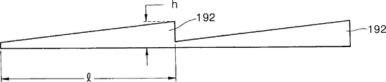
第一挡板30在整个表面上是由具有均匀厚度的单一的盘形元件形成。如图3所示,在第一挡板30中形成多个第一通孔32和多个第二通孔34。多个第一通孔32形成在第一位置,所述第一位置接近第一挡板30的中心轴线31,在径向与中心线31分开第一距离d1。多个第二通孔34形成在第二位置,所述第二位置接近第一挡板30的边,在径向与中心线31分开第二距离d2,d2大于d1。如图4所示,在第二挡板40的整个表面上以均匀的密度形成多个通孔42。第一和第二挡板30和40可以由铝制造。The
如图1所示,导向挡板50在第一挡板30上相对于第一挡板30同轴设置。在图5A-5C中示意示出导向挡板50上的结构。见图5A-5C,在导向挡板50的顶表面50a上形成一个入口52,通过它反应气体进入导向挡板50。通过入口52引入到导向挡板50内的反应气体通过多个路径53流到在导向挡板50的底50b上形成的多个出口54。As shown in FIG. 1 , the
在图1所示的这样构成的喷头中,产生被引入到反应室的反应气体的第一横向流动路径的第一间隙70,形成在第一挡板30和导向挡板50之间。第一间隙70的宽度由导向挡板50的底50b和第一挡板30的顶表面限制。而且,产生反应气体的第二横向流动路径的第二间隙80形成在第一和第二挡板30和40之间。第二间隙80的宽度由第一挡板30的底和第二挡板40的顶表面限制。In the thus constituted showerhead shown in FIG. 1 , a
图6示出分别形成在导向挡板50、第一挡板30和第二挡板40上的通孔54、32、34和42之间的位置关系。见图6,在径向与导向挡板的中心线51分开第三距离d3的导向挡板50的位置,形成多个出口54。第三距离d3大于第一距离d1,即,d1是第一通孔32分开导向挡板50中心轴线51的距离,并且小于第二距离d2,即,d2是第二通孔34离开相同轴线51的距离。最好是,在导向挡板50的出口54和第一挡板30的第一通孔32之间的距离小于出口54和第二通孔34之间的距离。这使得能够选择地控制反应气体量,以致流入到第一通孔32的反应气体量大于流入到第二通孔34的反应气体量,或通过调节在导向挡板50和第一挡板30之间的第一间隙70的宽度,使得第一和第二通孔32和34流量保持固定。即,因为出口54较靠近第一通孔32,所以在第一间隙70变得较窄时,较容易从出口54向第一通孔32引入反应气体,以致通过第一通孔32流动的反应气体量大于通过第二通孔34流动的反应气体量。因此,能够向晶片的中部供给比向它的边缘较大的反应气体量。另外,因为第一间隙70的宽度增加,通过出口54向第二通孔34排放并扩散的反应气体量增加,因此,增加通过第二通孔34流动的反应气体量。FIG. 6 shows the positional relationship among the through
为了电稳定所述喷头,第三挡板60设置在第二挡板40和面板20之间。第三挡板60可以由高电阻材料制造,例如碳化硅(SiC),它的电阻率足够地高,以便电稳定所述喷头。如图7所示,在第三挡板60的整个表面上以均匀的密度形成多个通孔62。In order to electrically stabilize the shower head, a third baffle 60 is disposed between the
第一垫圈环92确定第一间隙70的宽度,它是在导向挡板50和第一挡板30之间的第一挡板30的顶部边上设置的间隙控制器。第二间隙80的宽度由第二垫圈环94确定,它是在第一和第二挡板30和40之间第二挡板40的顶部边上设置的间隙控制器。The first spacer ring 92 defines the width of the
图8是环90的透视图。它是第一或第二垫圈环92或94的实施例。第一或第二垫圈环92或94的厚度由环90的厚度t确定。为了将第一和第二间隙70和80的宽度调节到希望的范围,第一或第二垫圈环92和94可以仅包括具有希望厚度的一个环90,或彼此重叠起来到达希望的厚度的具有预定厚度的两个或多个圆形环。FIG. 8 is a perspective view of ring 90 . It is an embodiment of the first or second gasket ring 92 or 94 . The thickness of the first or second gasket ring 92 or 94 is determined by the thickness t of the ring 90 . In order to adjust the width of the first and
第一挡板30的位置和第一间隙70的宽度可以由垫圈环92的厚度确定。在第一间隙70的宽度降低时,在第一挡板30中,通过第一通孔32流动的反应气体量大于通过第二通孔34流动的反应气体量。相反地,在第一间隙70的宽度增加时,在第一挡板中,通过第二通孔34的反应气体量增加。The position of the
而且,在第一和第二挡板30和40之间形成的第二间隙80的宽度由第二垫圈环94的厚度确定。在第二间隙80的宽度减小时,在多个通孔42当中,通过在第一挡板30的第一或第二通孔32或34附近的通孔42的反应气体量增加,从而使得通过多个通孔42的反应气体量变为有选择地不均匀,和在处理区域内的位置有关。相反地,在第二间隙80的宽度增加到足够程度时,则通过多个通孔42的反应气体量可以在整个处理区域变为均匀。Also, the width of the
图9A示出具有圆弧接触部分194的环190的透视图,在部分194中形成多个锯齿192,这是第一或第二垫圈环92或94的另一个实施例。图9B示出沿图9A的9B-9B的整个长度取的环190的侧视图。FIG. 9A shows a perspective view of a
见图9A和9B,设计锯齿192使其具有与90度中心角(*)的弧长l相同的节距。在环接触部分194上形成的锯齿192的高度约为0.01-0.5毫米。9A and 9B, the
如果在第一间隙70中的第一垫圈环92由环190组成,在其上形成多个锯齿192的环接触部分194可以设置成与第一挡板30或导向挡板50相对。如果环接触部分194在第一间隙70内与第一挡板30相对,则与锯齿192啮合的垫圈环耦接件形成在由环190构成的第一垫圈环92相对面的第一挡板30的表面上。If the first gasket ring 92 in the
图10示出改进的第一挡板130,其中已形成了连接环形接触部分194的垫圈环耦接件132。与环接触部分194的多个锯齿192啮合的多个锯齿(未示出)形成在垫圈环耦接件132上。与环190相同,在垫圈环耦接件132上形成的锯齿被设计成具有与90度的弧长相同的节距。在垫圈环耦接件132上形成的锯齿的高度约为0.01-0.05毫米。FIG. 10 shows a modified
而且,如果在第二间隙80中的第二垫圈环94由环190构成,则在其上形成多个锯齿192的环接触部分194可以设置成与第一或第二挡板30或40相对。如果环形接触部分194在第二间隙80内与第二挡板40相对地设置,则与锯齿192啮合的垫圈环耦接件形成在第二挡板40的与由环190构成的第二垫圈环94相对的表面上。Also, if the second gasket ring 94 in the
图11示出改进的挡板140,在其上已形成了与环接触部分194连接的垫圈环耦接件142。与环接触部分194的多个锯齿192啮合的多个锯齿(未示出)形成在垫圈环耦接件142上。与环190相似,在垫圈环耦接件142上形成的锯齿被设计成具有与90度的弧长相同的节距。在垫圈环耦接件142上形成的锯齿的高度约为0.01-0.05毫米。FIG. 11 shows a modified
图12A和12B示出喷头的部分示意图,用于说明被设置在第一挡板30和改进的第二挡板140之间的第二垫圈环94由环190构成时,使用环190控制第二间隙80的宽度的方法。图12A示出第二间隙80具有最小宽度的一个状态。如果在图12A所示的状态,环190在箭头‘a’所示的方向旋转,或改进的第二挡板140在箭头‘b’所示方向旋转,如图12B所示,则第二间隙80的宽度根据它的旋转距离增加Δw。因此,通过控制环190或改进的第二挡板140的旋转距离,将第二间隙80的宽度调节到希望的程度。Figures 12A and 12B show partial schematic views of the spray head for illustrating the use of the
图13A和13B示出沿图11的线13A-13A取的剖视图,用于说明改进的第二挡板140的垫圈环耦接件142。见图13A,在相邻的两个锯齿彼此相遇的、改进的第二挡板140上的垫圈环耦接件142的低台阶部分142,比改进的第二挡板140的顶部中心部分140a薄。见图13B,在改进的第二挡板140上,垫圈环耦接件142的每个锯齿的最高齿部分142b比改进的第二挡板140的顶部中心部分140a厚。13A and 13B show cross-sectional views taken along line 13A-13A of FIG. 11 for illustrating the gasket ring coupling 142 of the modified
为了用环190控制第二间隙80的宽度,如果环190的环接触部分194位于第一挡板30的对面,则在第一挡板30的底边上形成垫圈环耦接件,它具有与与改进的第二挡板140的顶部边缘上形成的垫圈环耦接件142相同的结构。因为该垫圈环耦接件与改进的第二挡板140的垫圈环耦接件142的结构相似,故省略它的详细说明。差别是,如果环190的环接触部分194设置在第一挡板30的对面,则环接触部分194接触第一挡板30的底,并且第一挡板30的垫圈环耦接件的一个部分的厚度小于第一挡板30的底面中心部分的厚度。In order to control the width of the
虽然已然就利用环190控制第二间隙80的宽度说明了本发明,但是,本领域的技术人员应理解,上述结构或设置也可以以相同的方式用于利用环190控制第一间隙70的宽度。Although the present invention has been described with regard to utilizing the
在上述实施例中,第一挡板30是由具有在整个表面上具有均匀厚度的单一的盘形元件制造的。但是,根据应用类型第一挡板30也可按各种方式构成。In the above-described embodiment, the
图14A和14B示出改进的第一挡板230的结构。图14A示出沿改进的第一挡板230的中心轴线231取的剖面图。图14B表示出改进的第一挡板230的分解透视图。14A and 14B show the structure of a modified
见图14A和14B,改进的第一挡板230包括:盘形的底板232,它具有在它的顶表面中心提供圆形空间的槽236;和盘形插入板234,被插入到槽236中,使得它能够在槽26内围绕改进的第一挡板230的中心轴线231旋转。插入板234被连接到用于旋转插入板234预定角度的驱动装置(未示出)。14A and 14B, the improved
底板232具有多个第一通孔237,和多个第二通孔238。多个第一通孔237形成在第一位置,所述第一位置靠近改进的第一挡板230的中心轴线231,并且在径向与中心轴线231分开第一距离d1,这个距离d1小于插入板234的半径。多个第二通孔238在第二位置形成,所述第二位置靠近底板232的边缘并且径向离开中心轴线231第二距离d2,这个距离大于插入板234的半径。插入板234具有多个通孔235,它们可以与在底板232上形成的多个第一通孔237连通。为了改变取决于插入板234的旋转距离的第一通孔的237的开放比,仅在相对于改进的第一底板230的中心轴线231的某些角度范围中有选择地形成插入板234中的多个通孔235和底板232中的多个通孔237。即,在插入板234中形成的所有或一些通孔235,可以根据插入板234的旋转距离,与底板232中形成的第一通孔237连通。The
通过采用具有上述结构的改进的第一挡板230,依据插入板234的旋转距离改变在底板232中形成的第一通孔237的开放比,从而调节从反应室的处理区域向晶片的中心部分供给的反应气体量。By adopting the improved
图15示意示出根据本发明的第二实施例的喷头的主要部分的结构。除了用第一和第二驱动轴292和294作为确定第一和第二间隙70和80的间隙控制器外,第二实施例与第一实施例相似。在图15所示的实施例中,间隙控制器包括第一和第二驱动轴292和294。第一驱动轴292选择地上下移动导向挡板50,以便确定第一间隙70的宽度。第二驱动轴294有选择地上下移动第一底板30,以便确定第二间隙80的宽度。第二驱动轴294相对于第一驱动轴292同轴设置。导向板50或第一挡板30上下移动的距离彼此相对地调节,从而确定第一或第二间隙70或80的宽度。通过考虑从反应室的处理区域向晶片的中心部分或边缘供给的反应气体量确定第一或第二间隙70或80的宽度。用第一和第二驱动轴292和294分别确定第一和第二间隙70和80的宽度,从而自由地调节从处理区域向晶片的中心部分或边缘供给的反应气体量。而且,这能够根据应用类型,使得供给的反应气体量在整个晶片表面上均匀或不均匀。Fig. 15 schematically shows the structure of a main part of a shower head according to a second embodiment of the present invention. The second embodiment is similar to the first embodiment except that the first and
图16A-16C示意地示出本发明的第三实施例喷头的主要部件的结构。见图16A,使用提升机构392和旋转机构394作为确定第一和第二间隙70和80的间隙控制器。除了提升机构392和旋转机构394外,在此实施例中的喷头部件与上述实施例的结构相同。提升机构392使用第一步进电动机312上下驱动第一挡板30,以便确定第二间隙80的宽度。旋转机构394使用第二步进电动机314,利用齿轮传动,上下驱动导向挡板50。16A-16C schematically show the structure of the main parts of the spray head of the third embodiment of the present invention. Referring to FIG. 16A , a lifting mechanism 392 and a rotating mechanism 394 are used as gap controllers for determining the first and
如图16A所示,提升机构392与旋转机构394集成在一起。第一步进电动机312传输的动力使得提升机构392能够上下移动。提升机构392包括:轴382,它穿过导向挡板50和第一挡板30;向外的突缘384,形成在轴382的一端,用于上下驱动第一挡板30,跟随轴382的上下移动。As shown in FIG. 16A , a lifting mechanism 392 is integrated with a rotating mechanism 394 . The power transmitted by the first stepping motor 312 enables the lifting mechanism 392 to move up and down. Lifting mechanism 392 comprises: shaft 382, and it passes
旋转机构394包括:轴382,它能够由第二步进电动机314传输的动力旋转;和外螺丝372,它形成在结合导向挡板50的轴382的外圆周的位置上,用于根据轴382的旋转,上下驱动导向挡板50。The rotation mechanism 394 includes: a shaft 382 capable of rotating by the power transmitted by the second stepping motor 314; The rotation of the
如图16B所示,轴382穿过的中心孔350形成在导向挡板50的中心部分。与螺丝372外螺纹配合的内螺纹352形成在中心孔350的内壁上。As shown in FIG. 16B , a
如图16C所示,在第一挡板30的中心部分,轴382穿过的中心孔332与容纳轴382端上形成的外突缘384的圆形空间334连通。As shown in FIG. 16C , at the central portion of the
用提升机构392调节第二间隙80的宽度。此时,如果轴382由提升机构392上下移动,以便提升或下降第一挡板30,则导向挡板50被提升或下降,跟随轴382的上下移动,因为接合螺丝372外螺纹的内螺纹352形成在导向挡板50中。因此,在轴382上下移动时,第一挡板30和导向挡板50同时上下移动。The width of the
用旋转机构394调节第一间隙70的宽度。如果用旋转机构394旋转轴382,则通过轴382的螺丝372的外螺纹和在导向挡板50的中心孔350中形成的内螺纹352的相互作用使得导向挡板50提升或下降。在轴382被旋转机构394这样旋转时,第一挡板30不旋转,而是保持静止,因为容纳向外突缘384的圆形空间334形成在第一挡板30中,使得向外突缘384的旋转不影响第一挡板30。在此,为了在旋转机构394旋转轴382时上下移动导向挡板50,而不是旋转它,在导向挡板50上连接止动器354,防止导向挡板50旋转。The width of the
在上述结构中,用提升机构392和旋转机构394分别确定第二和第一间隙80和70的宽度,使得按照希望地调节从处理区域向晶片的中心部分或边缘供给的气体量,或依据应用类型,使得供给的气体量在整个晶片表面上均匀或不均匀。In the above structure, the widths of the second and
图17示意示出根据本发明第四实施例的喷头主要件的结构。在图17中,相同的元件用相同的符号表示,并省略详细说明。Fig. 17 schematically shows the structure of the main part of the shower head according to the fourth embodiment of the present invention. In FIG. 17, the same elements are denoted by the same symbols, and detailed description thereof will be omitted.
在图17的实施例中,第一挡板430接触第二挡板440。因此,在第一和第二挡板430和440之间设置的第二间隙80的宽度实际上为零。设置同时上下驱动第一和第二挡板430和440的驱动轴480,以便确定在导向挡板50和第一挡板430之间形成的第一间隙70的宽度。在驱动轴480上下驱动第二挡板440时,第一挡板430被上下移动,跟随第二挡板440的上下移动,从而通过挡板50的底部和第一挡板430的顶部限制第一间隙70的宽度。导向挡板50的详细结构如上所述。In the embodiment of FIG. 17 , the
旋转机构490连接第一挡板430。旋转机构490在预定角度范围内使得第一挡板430相对于第二挡板440能够旋转。具体地,旋转机构490改变第一挡板430的旋转角,以致第一挡板和第二挡板430和440彼此以各种旋转角度接触。The
图18示出第一挡板430的顶视图。第一挡板430具有多个通孔432。排列多个通孔432,根据从第一挡板430的中心轴线431算起的半径,具有不同的开放比。FIG. 18 shows a top view of the
第一挡板430被分成多个扇形区域435a、435b和435c,它们从它的中心轴线431径向延伸。各多个扇形区域435a、435b和435c中的每一个都具有多个通孔432,它们仅形成在离开中心轴线431选择的半径的预定的范围内。即,扇形区域435a具有仅在离开中心轴线432第一半径r1的第一范围436a内形成的多个通孔432。扇形区域435b具有仅在离开中心轴线432第二半径r2的第二范围436b内形成的多个通孔432。扇形区域435c具有仅在离开中心轴线432第三半径r3的第三范围436c内形成的通孔432。The
图19示出第二挡板440的顶视图。第二挡板440具有多个通孔442。排列多个通孔442,以便根据第一挡板430围绕第二挡板440的中心轴线441旋转的距离具有不同的开放比。FIG. 19 shows a top view of the
第二挡板440被分成在它的中心轴线441的径向延伸的多个扇形区域445a、445b和445c。形成在第二挡板440上的多个扇形区域445a、445b和445c每个的大小与在第一挡板430上形成的多个扇形区域435a、435b和435c中的每个相对应。扇形区域445b和445c具有零的开放比(即不开放)。扇形区域445a具有以规则间隔排列的多个通孔442。The
因为如图17所示,第一和第二挡板430和440彼此接触,所以在第一挡板430上形成的多个通孔432中的选择的一些通孔与多个通孔442的选择的一些通孔连通,因此形成对准孔。依照第一挡板430被旋转机构490旋转的距离改变各对准孔的开放位置。Since the first and
图20A-20C示出在第一挡板和第二挡板430和440彼此以不同的旋转距离接触时的第二挡板440的底视图。即,图20A-20C示出,在旋转机构490将第一挡板430旋转在各角度的同时,第一挡板430接触第二挡板440时形成的对准孔的位置的改变。20A-20C illustrate bottom views of the
具体而论,图20A示出的状态是,第一挡板430被旋转机构490旋转预定角度距离,使得第一挡板430的扇形区域435a和第二挡板440的扇形区域445a彼此重叠。此时,在第一挡板430的扇形区域435a当中,仅在第一范围436a中形成的多个通孔432连通在第二挡板440的扇形区域445a中形成的多个通孔442。其结果,仅在第一范围436a中形成对准孔452,在第二挡板440中的其余的通孔442被第一挡板430阻挡。因此,如图20A所示,在第一挡板430接触第二挡板440时,从反应室内的处理区域向晶片上的边缘供给较大量的反应气体。Specifically, FIG. 20A shows a state where the
图20B示出的状态是,第一挡板430被旋转机构490旋转预定角度距离,以致第一挡板430的扇形区域435b和第二挡板440的扇形区域445a彼此重叠。此时,在第一挡板430的扇形区域435a当中,仅在第二范围436b中形成的多个通孔442与在第二挡板440的扇形区域445a中形成的多个通孔442连通。其结果,仅在第二范围436b中形成对准孔452,在第二挡板440中的其余的通孔442被第一挡板430阻挡。因此,如图20B所示,第一挡板430接触第二挡板440时,从反应室内的处理区域向晶片上的中心区域和边缘之间的中间区域供给较大量的反应气体。20B shows a state where the
图20C示出的状态是,第一挡板430被旋转机构490旋转预定角度距离,以致第一挡板430的扇形区域435c和第二挡板440的扇形区域445a彼此重叠。此时,在第一挡板430的扇形区域435c当中,仅在第三范围436c中形成的多个通孔432与在第二挡板440的扇形区域445a中形成的多个通孔442连通。其结果,仅在第三范围436中形成对准孔452,在第二挡板440中形成的其余的通孔442被第一挡板430阻挡。因此,如图20C所示,第一挡板430接触第二挡板440时,反应室内从处理区域向晶片上的接近中心部分的区域供给较大量的反应气体。FIG. 20C shows a state where the
如上所述,通过第一和第二挡板430和440的重叠形成的对准孔452的开放位置,随着由旋转机构490改变的第一挡板的旋转距离而变化。因此,为了调节向处理区域内的晶片上的特定位置供给的反应气体量,使用旋转机构490来控制第一挡板430的旋转角,这样便选择了对准孔452的开放位置。As described above, the open position of the alignment hole 452 formed by the overlapping of the first and
图21示出本发明第五实施例的喷头的主要件的结构的剖面图。在图21中,相同的元件用相同的符号表示,省略详细说明。Fig. 21 is a sectional view showing the structure of main parts of a shower head according to a fifth embodiment of the present invention. In FIG. 21, the same elements are denoted by the same symbols, and detailed description thereof will be omitted.
与图1所示的第一实施例相似,图21的第五实施例的喷头包括:第一挡板530,它设置在顶板10和面板20中间;和第二挡板540,设置在第一挡板530和面板30之间。第二挡板540具有顶表面,它限制在第一和第二挡板530和540之间形成反应气体流动通道的第二间隙80。为了控制通过在第一和第二挡板530和540之间形成的第二间隙80的反应气体量,在第二挡板540的顶表面上设置多个压电元件582、584和586。Similar to the first embodiment shown in FIG. 1, the shower head of the fifth embodiment in FIG. 21 includes: a
图22示出第一挡板530的顶视图。如图22所示,第一挡板530具有多个第一、第二和第三通孔532、534和536。多个第一通孔532形成的位置与第一挡板530的中心轴线531离开第一半径R1。多个第二通孔534形成的位置与第一挡板530的中心轴线531离开第二半径R2。R2>R1。多个第三通孔536形成的位置与第一挡板530的中心轴线531离开第三半径R3,R3>R2。FIG. 22 shows a top view of the
图23是第二挡板540的顶视图。如图23所示,第二挡板540分别具有第四通孔542,和多个第五、第六和第七通孔544、546和548。第四通孔542形成在第二挡板540的中心轴线541的位置上。形成多个第五通孔544的位置与中心轴线541离开第四半径R4。形成多个第六通孔546的位置与中心轴线541离开第五半径R5,R5>R4。形成多个第七通孔548的位置与中心轴线541离开第六半径R6,R6>R5。FIG. 23 is a top view of the
多个压电元件582、584和586包括:第一环形压电元件582,设置在第二挡板540上的第四和第五通孔542和544之间;第二压电元件584,设置在第二挡板540上的第五和第六通孔544和546之间;和第三压电元件586,设置在第二挡板540上的第六和第七通孔546和548之间。第一到第三压电元件582、584和586结合到第二挡板540。在第二挡板540上第一压电元件582设置的位置,与形成第一挡板530的多个第一通孔532的位置相对应。在第二挡板540上第二压电元件584设置的位置与形成第一挡板530的多个第二通孔534的位置相对应。在第二挡板540上第三压电元件586设置的位置与形成第一挡板530的多个第三通孔536的位置相对应。A plurality of
图24示出图21的一个部分“A”的放大图。见图21-24,各多个压电元件582、584和586包括压电层572,它根据施加的电压以厚度扩展的方式振动。压电元件572可以由铅锆酸盐钛酸盐(PZT)、PbTiO3、BaTiO3或聚偏氟乙烯(PVDF)聚合物制造。压电层572在两侧具有分别形成第一和第二电极574和576的两个主面。在邻近第一挡板530的第一电极574上形成绝缘层578。第二电极576由第二挡板540构成。即,第二挡板540另外起第二电极576的作用。因此,压电元件582包括在压电层572和第二挡板540之间的结合表面。此时,第二挡板540最好是由铝制造。FIG. 24 shows an enlarged view of a portion "A" of FIG. 21 . 21-24, each plurality of
电源单元590的电压施加到压电元件582、584和586上。各压电元件582、584和586的压电层572的厚度膨胀速率可以由电源单元590施加的电压电平控制。压电层572的厚度膨胀速率调节在压电元件582和第一通孔532之间的距离,因而调节从第一挡板530的第一通孔532向第二间隙80流动的反应气体量。因为压电层572的厚度膨胀速率是通过调节电源单元590供给的电压电平控制的,所以供给的电压有选择地打开或关闭第一挡板530的第一通孔532。第一压电元件582的上述结构相似地用于第二和第三压电元件584和586。采用所述的配置不仅能够选择地打开或关闭在第一挡板530上形成的第一到第三通孔532、534和536当中的离开第一挡板530的中心轴线531希望的半径的一些通孔,而且还能够调节通过所述通孔流动的反应气体量。因此,根据在反应室的处理区域内晶片上的特定位置所需的反应气体量,使用压电元件582、584和586,它们各具有随施加电压电平变化的厚度膨胀速率,能够选择地控制通过第一挡板530上形成的第一到第三多个通孔532、534和536流动的反应气体量。The voltage of the
虽然没有示出,但是参照图21说明的结构的喷头还可以包括参照图5A-5C说明过的、在第一挡板530上设置的导向挡板50。此时,在导向挡板50和第一挡板530之间形成与第一间隙70对应的间隙,从而提供反应气体的的横向流动通道。Although not shown, the shower head with the structure described with reference to FIG. 21 may further include the
喷头还可以包括第三挡板60,如参照图7所述地,它设置在第二挡板540和面板20之间。The spray head may further include a third baffle 60 disposed between the
如参照图21-24所述地,如果用压电元件582、584和586调节在第一和第二挡板530和540之间流动的反应气体量,则根据从电源单元590施加的电压的电平,从喷头的中心的径向调节供给的反应气体量。因此,在改进了调节供给的反应气体量的控制性能的情况下,在此喷头中不需要机械运动。21-24, if the
如上所述,根据本发明的喷头包括间隙控制器,它确定形成在相邻两个挡板之间的反应气体流动通道的间隙的宽度。通过所述间隙控制器有选择地降低或增加间隙宽度,从而调节向在反应室的处理区域中的晶片上特定位置供给的反应气体量,并根据应用类型,使得向晶片上的位置供给的气体量均匀或不均匀。As described above, the shower head according to the present invention includes the gap controller which determines the width of the gap of the reaction gas flow channel formed between two adjacent baffle plates. The gap width is selectively decreased or increased by the gap controller, thereby adjusting the amount of reactant gas supplied to a specific location on the wafer in the processing region of the reaction chamber, and depending on the type of application, such that the gas supplied to the location on the wafer uniform or uneven.
因此,根据本发明,较容易地依据在晶片上的位置调节反应气体的分布,以便在制造半导体器件的过程中,在整个晶片表面上获得最佳的蚀刻速率均匀度。而且,本发明使得能够自由地调节供给的反应气体量,从而预先对在蚀刻步骤中,在晶片上中可能部分地发生的蚀刻速率均匀性的减低进行补偿。因此,本发明步不仅自由地优化了依赖于在晶片上的位置的图案的均匀度,而且不需要非常多地考虑在整个晶片表面上的均匀度,从而降低在开发半导体器件制造设备中的时间和花费。Therefore, according to the present invention, it is easier to adjust the distribution of the reactant gas according to the position on the wafer in order to obtain the optimum etch rate uniformity over the entire wafer surface during the manufacture of semiconductor devices. Furthermore, the present invention enables free adjustment of the amount of supplied reaction gas, thereby compensating in advance for a decrease in uniformity of etching rate that may partially occur on a wafer during an etching step. Therefore, the present invention not only freely optimizes the uniformity of the pattern depending on the position on the wafer, but also does not need to take very much consideration of the uniformity over the entire wafer surface, thereby reducing time in developing semiconductor device manufacturing equipment. and spend.
已公开了本发明的优选实施例,虽然使用了特定的术语,但是使用它们仅是为了解释原理,而不是限定。因此,本领域的技术人员应理解,不偏离权利要求的本发明的精神和范围可以做出形式和细节中的各种改变。Preferred embodiments of this invention have been disclosed, and although specific terms are used, they are used for the purpose of explanation of principles only and not limitation. Accordingly, it will be understood by those skilled in the art that various changes in form and details may be made therein without departing from the spirit and scope of the present invention as claimed.
Claims (108)
Applications Claiming Priority (2)
| Application Number | Priority Date | Filing Date | Title |
|---|---|---|---|
| KR10-2001-0042822A KR100400044B1 (en) | 2001-07-16 | 2001-07-16 | Shower head of wafer treatment apparatus having gap controller |
| KR42822/2001 | 2001-07-16 |
Related Child Applications (1)
| Application Number | Title | Priority Date | Filing Date |
|---|---|---|---|
| CNB2005101135327A Division CN100435274C (en) | 2001-07-16 | 2002-07-16 | Showerhead for wafer processing equipment with gap controller |
Publications (2)
| Publication Number | Publication Date |
|---|---|
| CN1397991A true CN1397991A (en) | 2003-02-19 |
| CN1265441C CN1265441C (en) | 2006-07-19 |
Family
ID=36772450
Family Applications (2)
| Application Number | Title | Priority Date | Filing Date |
|---|---|---|---|
| CNB021268762A Expired - Fee Related CN1265441C (en) | 2001-07-16 | 2002-07-16 | Showerhead for wafer processing equipment with gap controller |
| CNB2005101135327A Expired - Fee Related CN100435274C (en) | 2001-07-16 | 2002-07-16 | Showerhead for wafer processing equipment with gap controller |
Family Applications After (1)
| Application Number | Title | Priority Date | Filing Date |
|---|---|---|---|
| CNB2005101135327A Expired - Fee Related CN100435274C (en) | 2001-07-16 | 2002-07-16 | Showerhead for wafer processing equipment with gap controller |
Country Status (6)
| Country | Link |
|---|---|
| US (2) | US6872258B2 (en) |
| JP (2) | JP4246450B2 (en) |
| KR (1) | KR100400044B1 (en) |
| CN (2) | CN1265441C (en) |
| DE (1) | DE10232206B4 (en) |
| TW (1) | TW565903B (en) |
Cited By (13)
| Publication number | Priority date | Publication date | Assignee | Title |
|---|---|---|---|---|
| CN100416756C (en) * | 2005-12-05 | 2008-09-03 | 北京北方微电子基地设备工艺研究中心有限责任公司 | Plasma etching device |
| CN102193565A (en) * | 2010-03-19 | 2011-09-21 | 上海微电子装备有限公司 | Air bath temperature control device and method |
| CN102931050A (en) * | 2011-08-10 | 2013-02-13 | 中国科学院微电子研究所 | A New Air Intake Method of Atmospheric Pressure Plasma Radical Cleaning Spray Gun |
| CN102051595B (en) * | 2009-10-29 | 2013-04-03 | 无锡华润上华半导体有限公司 | Chemical vapor deposition device and spray nozzle thereof |
| CN101940067B (en) * | 2008-02-08 | 2013-04-03 | 朗姆研究公司 | A Mechanism for Adjusting Electrode Azimuth and Parallelism of Plasma Processing System |
| CN103147071A (en) * | 2011-12-07 | 2013-06-12 | 台湾积体电路制造股份有限公司 | Chemical vapor deposition film profile uniformity control |
| CN103184432A (en) * | 2011-12-30 | 2013-07-03 | 中芯国际集成电路制造(北京)有限公司 | Injection device and processing apparatus |
| CN103198993A (en) * | 2012-01-09 | 2013-07-10 | 中微半导体设备(上海)有限公司 | Gas spray head used for plasma processing device |
| CN105091506A (en) * | 2015-08-31 | 2015-11-25 | 武汉华星光电技术有限公司 | Vacuum drying device |
| CN109786202A (en) * | 2017-11-15 | 2019-05-21 | 台湾积体电路制造股份有限公司 | The method and etch system being etched with reactor |
| CN110621411A (en) * | 2017-05-31 | 2019-12-27 | 艾斯曲尔医疗公司 | Nozzle device and method for manufacturing the same |
| CN112689376A (en) * | 2021-03-15 | 2021-04-20 | 四川大学 | Microwave plasma jet excitation device adopting piezoelectric material |
| TWI825543B (en) * | 2020-12-31 | 2023-12-11 | 中國大陸商拓荆科技股份有限公司 | Gas nozzle with controllable air flow distribution |
Families Citing this family (543)
| Publication number | Priority date | Publication date | Assignee | Title |
|---|---|---|---|---|
| DE60231601D1 (en) * | 2001-01-22 | 2009-04-30 | Tokio Electron Ltd | DEVICE AND METHOD FOR TREATMENT |
| EP1421606A4 (en) * | 2001-08-06 | 2008-03-05 | Genitech Co Ltd | PLASMA ACTIVE ATOMIC LAYER (PEALD) DEPOSITION APPARATUS AND METHOD OF FORMING THIN FILM USING SAID APPARATUS |
| US6820570B2 (en) * | 2001-08-15 | 2004-11-23 | Nobel Biocare Services Ag | Atomic layer deposition reactor |
| KR100760291B1 (en) * | 2001-11-08 | 2007-09-19 | 에이에스엠지니텍코리아 주식회사 | Thin film formation method |
| KR100426816B1 (en) * | 2002-07-31 | 2004-04-14 | 삼성전자주식회사 | Plasma processing equipment having improved vacuum pressure control apparatus |
| US20040031565A1 (en) * | 2002-08-13 | 2004-02-19 | Taiwan Semiconductor Manufacturing Co., Ltd. | Gas distribution plate for processing chamber |
| US7252738B2 (en) * | 2002-09-20 | 2007-08-07 | Lam Research Corporation | Apparatus for reducing polymer deposition on a substrate and substrate support |
| US20040082251A1 (en) * | 2002-10-29 | 2004-04-29 | Applied Materials, Inc. | Apparatus for adjustable gas distribution for semiconductor substrate processing |
| US7316761B2 (en) * | 2003-02-03 | 2008-01-08 | Applied Materials, Inc. | Apparatus for uniformly etching a dielectric layer |
| KR100526928B1 (en) * | 2003-07-16 | 2005-11-09 | 삼성전자주식회사 | Etching Apparatus |
| US20050183824A1 (en) * | 2004-02-25 | 2005-08-25 | Advanced Display Process Engineering Co., Ltd. | Apparatus for manufacturing flat-panel display |
| US20050241767A1 (en) * | 2004-04-30 | 2005-11-03 | Ferris David S | Multi-piece baffle plate assembly for a plasma processing system |
| KR100562306B1 (en) * | 2004-09-13 | 2006-03-22 | 동부아남반도체 주식회사 | Chemical mechanical polishing equipment |
| US20060138925A1 (en) * | 2004-12-28 | 2006-06-29 | Yi-Fang Cheng | Plasma processing device having a ring-shaped air chamber for heat dissipation |
| US7608549B2 (en) * | 2005-03-15 | 2009-10-27 | Asm America, Inc. | Method of forming non-conformal layers |
| CN100595973C (en) * | 2005-03-30 | 2010-03-24 | 松下电器产业株式会社 | Transmission Line Pairs and Transmission Line Groups |
| JP5055114B2 (en) * | 2005-03-30 | 2012-10-24 | パナソニック株式会社 | Plasma doping method |
| KR101153161B1 (en) * | 2005-04-01 | 2012-06-18 | 주성엔지니어링(주) | Gas injector and Apparatus including the same for fabricating Liquid Crystal Display Device |
| US7396415B2 (en) * | 2005-06-02 | 2008-07-08 | Asm America, Inc. | Apparatus and methods for isolating chemical vapor reactions at a substrate surface |
| JP2007042951A (en) * | 2005-08-04 | 2007-02-15 | Tokyo Electron Ltd | Plasma processing equipment |
| KR100725613B1 (en) | 2005-10-27 | 2007-06-08 | 주식회사 래디언테크 | Baffle and Plasma Treatment Device Having the Same |
| US7850779B2 (en) | 2005-11-04 | 2010-12-14 | Applied Materisals, Inc. | Apparatus and process for plasma-enhanced atomic layer deposition |
| US20070163716A1 (en) * | 2006-01-19 | 2007-07-19 | Taiwan Semiconductor Manufacturing Co., Ltd. | Gas distribution apparatuses and methods for controlling gas distribution apparatuses |
| US20070227666A1 (en) * | 2006-03-30 | 2007-10-04 | Tokyo Electron Limited | Plasma processing apparatus |
| KR100768673B1 (en) * | 2006-05-30 | 2007-10-22 | (주)위지트 | Shower head |
| KR101217522B1 (en) * | 2006-09-07 | 2013-01-02 | 주식회사 원익아이피에스 | A showerhead having a block for gas folw control |
| US20080087641A1 (en) * | 2006-10-16 | 2008-04-17 | Lam Research Corporation | Components for a plasma processing apparatus |
| CN101179005B (en) * | 2006-11-10 | 2010-10-27 | Tes股份有限公司 | Exhaust air system, semi-conductor manufacturing installation for manufacturing thin film by the same and method thereof |
| US11136667B2 (en) | 2007-01-08 | 2021-10-05 | Eastman Kodak Company | Deposition system and method using a delivery head separated from a substrate by gas pressure |
| US7767028B2 (en) * | 2007-03-14 | 2010-08-03 | Lam Research Corporation | Cleaning hardware kit for composite showerhead electrode assemblies for plasma processing apparatuses |
| US20080241387A1 (en) * | 2007-03-29 | 2008-10-02 | Asm International N.V. | Atomic layer deposition reactor |
| US20090035946A1 (en) * | 2007-07-31 | 2009-02-05 | Asm International N.V. | In situ deposition of different metal-containing films using cyclopentadienyl metal precursors |
| KR20090018290A (en) * | 2007-08-17 | 2009-02-20 | 에이에스엠지니텍코리아 주식회사 | Deposition equipment |
| KR100901118B1 (en) * | 2007-08-24 | 2009-06-08 | 주식회사 케이씨텍 | Injection unit of thin film deposition apparatus |
| US8673080B2 (en) | 2007-10-16 | 2014-03-18 | Novellus Systems, Inc. | Temperature controlled showerhead |
| US9059223B2 (en) * | 2007-12-12 | 2015-06-16 | Intermolecular, Inc. | Modular flow cell and adjustment system |
| US7879183B2 (en) * | 2008-02-27 | 2011-02-01 | Applied Materials, Inc. | Apparatus and method for front side protection during backside cleaning |
| JP4956469B2 (en) * | 2008-03-24 | 2012-06-20 | 株式会社ニューフレアテクノロジー | Semiconductor manufacturing equipment |
| US8252114B2 (en) * | 2008-03-28 | 2012-08-28 | Tokyo Electron Limited | Gas distribution system and method for distributing process gas in a processing system |
| US8383525B2 (en) * | 2008-04-25 | 2013-02-26 | Asm America, Inc. | Plasma-enhanced deposition process for forming a metal oxide thin film and related structures |
| US8161906B2 (en) | 2008-07-07 | 2012-04-24 | Lam Research Corporation | Clamped showerhead electrode assembly |
| US8221582B2 (en) | 2008-07-07 | 2012-07-17 | Lam Research Corporation | Clamped monolithic showerhead electrode |
| US8206506B2 (en) * | 2008-07-07 | 2012-06-26 | Lam Research Corporation | Showerhead electrode |
| US20100112212A1 (en) * | 2008-10-31 | 2010-05-06 | Applied Materials, Inc. | Adjustable gas distribution apparatus |
| US10378106B2 (en) | 2008-11-14 | 2019-08-13 | Asm Ip Holding B.V. | Method of forming insulation film by modified PEALD |
| JP5150461B2 (en) * | 2008-11-14 | 2013-02-20 | 芝浦メカトロニクス株式会社 | Plasma processing equipment |
| US9394608B2 (en) | 2009-04-06 | 2016-07-19 | Asm America, Inc. | Semiconductor processing reactor and components thereof |
| US8402918B2 (en) * | 2009-04-07 | 2013-03-26 | Lam Research Corporation | Showerhead electrode with centering feature |
| US8272346B2 (en) | 2009-04-10 | 2012-09-25 | Lam Research Corporation | Gasket with positioning feature for clamped monolithic showerhead electrode |
| KR101110080B1 (en) * | 2009-07-08 | 2012-03-13 | 주식회사 유진테크 | Substrate treatment method for selectively inserting diffusion plate |
| JP5777615B2 (en) * | 2009-07-15 | 2015-09-09 | アプライド マテリアルズ インコーポレイテッドApplied Materials,Incorporated | Flow control mechanism of CVD chamber |
| US8802201B2 (en) | 2009-08-14 | 2014-08-12 | Asm America, Inc. | Systems and methods for thin-film deposition of metal oxides using excited nitrogen-oxygen species |
| US8419959B2 (en) * | 2009-09-18 | 2013-04-16 | Lam Research Corporation | Clamped monolithic showerhead electrode |
| KR101450015B1 (en) * | 2009-09-25 | 2014-10-13 | 어플라이드 머티어리얼스, 인코포레이티드 | Method and apparatus for high efficiency gas dissociation in inductive coupled plasma reactor |
| KR200464037Y1 (en) | 2009-10-13 | 2012-12-07 | 램 리써치 코포레이션 | - edge-clamped and mechanically fastened inner electrode of showerhead electrode assembly |
| US20110097489A1 (en) * | 2009-10-27 | 2011-04-28 | Kerr Roger S | Distribution manifold including multiple fluid communication ports |
| DE102010000388A1 (en) | 2010-02-11 | 2011-08-11 | Aixtron Ag, 52134 | Gas inlet element with baffle plate arrangement |
| US8573152B2 (en) | 2010-09-03 | 2013-11-05 | Lam Research Corporation | Showerhead electrode |
| US8845806B2 (en) * | 2010-10-22 | 2014-09-30 | Asm Japan K.K. | Shower plate having different aperture dimensions and/or distributions |
| CN103403843B (en) | 2011-03-04 | 2016-12-14 | 诺发系统公司 | Hybrid Ceramic Sprinklers |
| US9129778B2 (en) | 2011-03-18 | 2015-09-08 | Lam Research Corporation | Fluid distribution members and/or assemblies |
| US9245717B2 (en) | 2011-05-31 | 2016-01-26 | Lam Research Corporation | Gas distribution system for ceramic showerhead of plasma etch reactor |
| US8562785B2 (en) * | 2011-05-31 | 2013-10-22 | Lam Research Corporation | Gas distribution showerhead for inductively coupled plasma etch reactor |
| US9312155B2 (en) | 2011-06-06 | 2016-04-12 | Asm Japan K.K. | High-throughput semiconductor-processing apparatus equipped with multiple dual-chamber modules |
| US9793148B2 (en) | 2011-06-22 | 2017-10-17 | Asm Japan K.K. | Method for positioning wafers in multiple wafer transport |
| US10364496B2 (en) | 2011-06-27 | 2019-07-30 | Asm Ip Holding B.V. | Dual section module having shared and unshared mass flow controllers |
| JP5902896B2 (en) * | 2011-07-08 | 2016-04-13 | 東京エレクトロン株式会社 | Substrate processing equipment |
| US10854498B2 (en) | 2011-07-15 | 2020-12-01 | Asm Ip Holding B.V. | Wafer-supporting device and method for producing same |
| US20130023129A1 (en) | 2011-07-20 | 2013-01-24 | Asm America, Inc. | Pressure transmitter for a semiconductor processing environment |
| KR101879175B1 (en) * | 2011-10-20 | 2018-08-20 | 삼성전자주식회사 | Chemical Vapor Deposition Apparatus |
| US9017481B1 (en) | 2011-10-28 | 2015-04-28 | Asm America, Inc. | Process feed management for semiconductor substrate processing |
| JP5860063B2 (en) * | 2011-12-22 | 2016-02-16 | キヤノンアネルバ株式会社 | Substrate processing equipment |
| US8946830B2 (en) | 2012-04-04 | 2015-02-03 | Asm Ip Holdings B.V. | Metal oxide protective layer for a semiconductor device |
| CN103388132B (en) * | 2012-05-11 | 2015-11-25 | 中微半导体设备(上海)有限公司 | Gas shower head, its manufacturing method and thin film growth reactor |
| US9418866B2 (en) * | 2012-06-08 | 2016-08-16 | Tokyo Electron Limited | Gas treatment method |
| US9558931B2 (en) | 2012-07-27 | 2017-01-31 | Asm Ip Holding B.V. | System and method for gas-phase sulfur passivation of a semiconductor surface |
| US9659799B2 (en) | 2012-08-28 | 2017-05-23 | Asm Ip Holding B.V. | Systems and methods for dynamic semiconductor process scheduling |
| US9021985B2 (en) | 2012-09-12 | 2015-05-05 | Asm Ip Holdings B.V. | Process gas management for an inductively-coupled plasma deposition reactor |
| US9132436B2 (en) | 2012-09-21 | 2015-09-15 | Applied Materials, Inc. | Chemical control features in wafer process equipment |
| US9324811B2 (en) | 2012-09-26 | 2016-04-26 | Asm Ip Holding B.V. | Structures and devices including a tensile-stressed silicon arsenic layer and methods of forming same |
| US10714315B2 (en) | 2012-10-12 | 2020-07-14 | Asm Ip Holdings B.V. | Semiconductor reaction chamber showerhead |
| JP2014082354A (en) * | 2012-10-17 | 2014-05-08 | Hitachi High-Technologies Corp | Plasma processing apparatus |
| DE102012111218A1 (en) * | 2012-11-21 | 2014-05-22 | Emdeoled Gmbh | Material discharge head of material discharge device comprises material discharge surface comprising material discharge openings, and connecting channel for direct connection to the material discharge opening with material storage container |
| US9640416B2 (en) | 2012-12-26 | 2017-05-02 | Asm Ip Holding B.V. | Single-and dual-chamber module-attachable wafer-handling chamber |
| US20160376700A1 (en) | 2013-02-01 | 2016-12-29 | Asm Ip Holding B.V. | System for treatment of deposition reactor |
| US10256079B2 (en) | 2013-02-08 | 2019-04-09 | Applied Materials, Inc. | Semiconductor processing systems having multiple plasma configurations |
| US9589770B2 (en) | 2013-03-08 | 2017-03-07 | Asm Ip Holding B.V. | Method and systems for in-situ formation of intermediate reactive species |
| US9484191B2 (en) | 2013-03-08 | 2016-11-01 | Asm Ip Holding B.V. | Pulsed remote plasma method and system |
| US20140272135A1 (en) * | 2013-03-12 | 2014-09-18 | Taiwan Semiconductor Manufacturing Company Limited | Deposition injection masking |
| US9353439B2 (en) * | 2013-04-05 | 2016-05-31 | Lam Research Corporation | Cascade design showerhead for transient uniformity |
| KR102156795B1 (en) * | 2013-05-15 | 2020-09-17 | 에이에스엠 아이피 홀딩 비.브이. | Deposition apparatus |
| US8993054B2 (en) | 2013-07-12 | 2015-03-31 | Asm Ip Holding B.V. | Method and system to reduce outgassing in a reaction chamber |
| US9018111B2 (en) | 2013-07-22 | 2015-04-28 | Asm Ip Holding B.V. | Semiconductor reaction chamber with plasma capabilities |
| US9793115B2 (en) | 2013-08-14 | 2017-10-17 | Asm Ip Holding B.V. | Structures and devices including germanium-tin films and methods of forming same |
| US9240412B2 (en) | 2013-09-27 | 2016-01-19 | Asm Ip Holding B.V. | Semiconductor structure and device and methods of forming same using selective epitaxial process |
| US9556516B2 (en) | 2013-10-09 | 2017-01-31 | ASM IP Holding B.V | Method for forming Ti-containing film by PEALD using TDMAT or TDEAT |
| US10179947B2 (en) | 2013-11-26 | 2019-01-15 | Asm Ip Holding B.V. | Method for forming conformal nitrided, oxidized, or carbonized dielectric film by atomic layer deposition |
| KR101505948B1 (en) * | 2013-12-16 | 2015-03-26 | 피에스케이 주식회사 | A baffle assembly and an apparatus for treating a substrate with the baffle |
| KR101560623B1 (en) * | 2014-01-03 | 2015-10-15 | 주식회사 유진테크 | Substrate processing apparatus and substrate processing method |
| US10683571B2 (en) | 2014-02-25 | 2020-06-16 | Asm Ip Holding B.V. | Gas supply manifold and method of supplying gases to chamber using same |
| US10167557B2 (en) | 2014-03-18 | 2019-01-01 | Asm Ip Holding B.V. | Gas distribution system, reactor including the system, and methods of using the same |
| US9447498B2 (en) | 2014-03-18 | 2016-09-20 | Asm Ip Holding B.V. | Method for performing uniform processing in gas system-sharing multiple reaction chambers |
| US11015245B2 (en) | 2014-03-19 | 2021-05-25 | Asm Ip Holding B.V. | Gas-phase reactor and system having exhaust plenum and components thereof |
| US9404587B2 (en) | 2014-04-24 | 2016-08-02 | ASM IP Holding B.V | Lockout tagout for semiconductor vacuum valve |
| US10741365B2 (en) * | 2014-05-05 | 2020-08-11 | Lam Research Corporation | Low volume showerhead with porous baffle |
| US10858737B2 (en) | 2014-07-28 | 2020-12-08 | Asm Ip Holding B.V. | Showerhead assembly and components thereof |
| US9543180B2 (en) | 2014-08-01 | 2017-01-10 | Asm Ip Holding B.V. | Apparatus and method for transporting wafers between wafer carrier and process tool under vacuum |
| CN104195525B (en) * | 2014-08-15 | 2016-08-24 | 沈阳拓荆科技有限公司 | Two kinds of independent uniformly jet spray equipments of gas |
| US9890456B2 (en) | 2014-08-21 | 2018-02-13 | Asm Ip Holding B.V. | Method and system for in situ formation of gas-phase compounds |
| US9657845B2 (en) | 2014-10-07 | 2017-05-23 | Asm Ip Holding B.V. | Variable conductance gas distribution apparatus and method |
| US10941490B2 (en) | 2014-10-07 | 2021-03-09 | Asm Ip Holding B.V. | Multiple temperature range susceptor, assembly, reactor and system including the susceptor, and methods of using the same |
| US9966240B2 (en) | 2014-10-14 | 2018-05-08 | Applied Materials, Inc. | Systems and methods for internal surface conditioning assessment in plasma processing equipment |
| KR102300403B1 (en) | 2014-11-19 | 2021-09-09 | 에이에스엠 아이피 홀딩 비.브이. | Method of depositing thin film |
| US11637002B2 (en) | 2014-11-26 | 2023-04-25 | Applied Materials, Inc. | Methods and systems to enhance process uniformity |
| KR102263121B1 (en) | 2014-12-22 | 2021-06-09 | 에이에스엠 아이피 홀딩 비.브이. | Semiconductor device and manufacuring method thereof |
| US20160225652A1 (en) | 2015-02-03 | 2016-08-04 | Applied Materials, Inc. | Low temperature chuck for plasma processing systems |
| US9478415B2 (en) | 2015-02-13 | 2016-10-25 | Asm Ip Holding B.V. | Method for forming film having low resistance and shallow junction depth |
| US10529542B2 (en) | 2015-03-11 | 2020-01-07 | Asm Ip Holdings B.V. | Cross-flow reactor and method |
| US10276355B2 (en) | 2015-03-12 | 2019-04-30 | Asm Ip Holding B.V. | Multi-zone reactor, system including the reactor, and method of using the same |
| US10378107B2 (en) | 2015-05-22 | 2019-08-13 | Lam Research Corporation | Low volume showerhead with faceplate holes for improved flow uniformity |
| US10023959B2 (en) | 2015-05-26 | 2018-07-17 | Lam Research Corporation | Anti-transient showerhead |
| US10458018B2 (en) | 2015-06-26 | 2019-10-29 | Asm Ip Holding B.V. | Structures including metal carbide material, devices including the structures, and methods of forming same |
| US10600673B2 (en) | 2015-07-07 | 2020-03-24 | Asm Ip Holding B.V. | Magnetic susceptor to baseplate seal |
| US10043661B2 (en) | 2015-07-13 | 2018-08-07 | Asm Ip Holding B.V. | Method for protecting layer by forming hydrocarbon-based extremely thin film |
| US9899291B2 (en) | 2015-07-13 | 2018-02-20 | Asm Ip Holding B.V. | Method for protecting layer by forming hydrocarbon-based extremely thin film |
| US10083836B2 (en) | 2015-07-24 | 2018-09-25 | Asm Ip Holding B.V. | Formation of boron-doped titanium metal films with high work function |
| US10087525B2 (en) | 2015-08-04 | 2018-10-02 | Asm Ip Holding B.V. | Variable gap hard stop design |
| US9741593B2 (en) | 2015-08-06 | 2017-08-22 | Applied Materials, Inc. | Thermal management systems and methods for wafer processing systems |
| US9647114B2 (en) | 2015-08-14 | 2017-05-09 | Asm Ip Holding B.V. | Methods of forming highly p-type doped germanium tin films and structures and devices including the films |
| US9711345B2 (en) | 2015-08-25 | 2017-07-18 | Asm Ip Holding B.V. | Method for forming aluminum nitride-based film by PEALD |
| JP1545606S (en) * | 2015-08-26 | 2016-03-14 | ||
| US10504700B2 (en) | 2015-08-27 | 2019-12-10 | Applied Materials, Inc. | Plasma etching systems and methods with secondary plasma injection |
| US9960072B2 (en) | 2015-09-29 | 2018-05-01 | Asm Ip Holding B.V. | Variable adjustment for precise matching of multiple chamber cavity housings |
| KR102537309B1 (en) * | 2015-10-08 | 2023-05-25 | 어플라이드 머티어리얼스, 인코포레이티드 | Showerhead with reduced backside plasma ignition |
| US9909214B2 (en) | 2015-10-15 | 2018-03-06 | Asm Ip Holding B.V. | Method for depositing dielectric film in trenches by PEALD |
| US10211308B2 (en) | 2015-10-21 | 2019-02-19 | Asm Ip Holding B.V. | NbMC layers |
| KR102462931B1 (en) | 2015-10-30 | 2022-11-04 | 삼성전자주식회사 | Gas Supply Unit and Substrate Treating Apparatus |
| US10322384B2 (en) | 2015-11-09 | 2019-06-18 | Asm Ip Holding B.V. | Counter flow mixer for process chamber |
| US9455138B1 (en) | 2015-11-10 | 2016-09-27 | Asm Ip Holding B.V. | Method for forming dielectric film in trenches by PEALD using H-containing gas |
| US9905420B2 (en) | 2015-12-01 | 2018-02-27 | Asm Ip Holding B.V. | Methods of forming silicon germanium tin films and structures and devices including the films |
| US9607837B1 (en) | 2015-12-21 | 2017-03-28 | Asm Ip Holding B.V. | Method for forming silicon oxide cap layer for solid state diffusion process |
| US9627221B1 (en) | 2015-12-28 | 2017-04-18 | Asm Ip Holding B.V. | Continuous process incorporating atomic layer etching |
| US9735024B2 (en) | 2015-12-28 | 2017-08-15 | Asm Ip Holding B.V. | Method of atomic layer etching using functional group-containing fluorocarbon |
| US11139308B2 (en) | 2015-12-29 | 2021-10-05 | Asm Ip Holding B.V. | Atomic layer deposition of III-V compounds to form V-NAND devices |
| US9754779B1 (en) | 2016-02-19 | 2017-09-05 | Asm Ip Holding B.V. | Method for forming silicon nitride film selectively on sidewalls or flat surfaces of trenches |
| US10529554B2 (en) | 2016-02-19 | 2020-01-07 | Asm Ip Holding B.V. | Method for forming silicon nitride film selectively on sidewalls or flat surfaces of trenches |
| US10468251B2 (en) | 2016-02-19 | 2019-11-05 | Asm Ip Holding B.V. | Method for forming spacers using silicon nitride film for spacer-defined multiple patterning |
| JP6662998B2 (en) * | 2016-03-03 | 2020-03-11 | コアテクノロジー株式会社 | Plasma processing equipment |
| US10501866B2 (en) | 2016-03-09 | 2019-12-10 | Asm Ip Holding B.V. | Gas distribution apparatus for improved film uniformity in an epitaxial system |
| US10343920B2 (en) | 2016-03-18 | 2019-07-09 | Asm Ip Holding B.V. | Aligned carbon nanotubes |
| US9892913B2 (en) | 2016-03-24 | 2018-02-13 | Asm Ip Holding B.V. | Radial and thickness control via biased multi-port injection settings |
| US10533252B2 (en) * | 2016-03-31 | 2020-01-14 | Taiwan Semiconductor Manufacturing Co., Ltd. | Showerhead, semicondcutor processing apparatus having the same and semiconductor process |
| US10483092B2 (en) * | 2016-04-13 | 2019-11-19 | Lam Research Corporation | Baffle plate and showerhead assemblies and corresponding manufacturing method |
| US10865475B2 (en) | 2016-04-21 | 2020-12-15 | Asm Ip Holding B.V. | Deposition of metal borides and silicides |
| US10190213B2 (en) | 2016-04-21 | 2019-01-29 | Asm Ip Holding B.V. | Deposition of metal borides |
| US10087522B2 (en) | 2016-04-21 | 2018-10-02 | Asm Ip Holding B.V. | Deposition of metal borides |
| US10032628B2 (en) | 2016-05-02 | 2018-07-24 | Asm Ip Holding B.V. | Source/drain performance through conformal solid state doping |
| US10367080B2 (en) | 2016-05-02 | 2019-07-30 | Asm Ip Holding B.V. | Method of forming a germanium oxynitride film |
| KR102592471B1 (en) | 2016-05-17 | 2023-10-20 | 에이에스엠 아이피 홀딩 비.브이. | Method of forming metal interconnection and method of fabricating semiconductor device using the same |
| US10504754B2 (en) | 2016-05-19 | 2019-12-10 | Applied Materials, Inc. | Systems and methods for improved semiconductor etching and component protection |
| US11453943B2 (en) | 2016-05-25 | 2022-09-27 | Asm Ip Holding B.V. | Method for forming carbon-containing silicon/metal oxide or nitride film by ALD using silicon precursor and hydrocarbon precursor |
| US10388509B2 (en) | 2016-06-28 | 2019-08-20 | Asm Ip Holding B.V. | Formation of epitaxial layers via dislocation filtering |
| US9865484B1 (en) | 2016-06-29 | 2018-01-09 | Applied Materials, Inc. | Selective etch using material modification and RF pulsing |
| US10612137B2 (en) | 2016-07-08 | 2020-04-07 | Asm Ip Holdings B.V. | Organic reactants for atomic layer deposition |
| US9859151B1 (en) | 2016-07-08 | 2018-01-02 | Asm Ip Holding B.V. | Selective film deposition method to form air gaps |
| US9793135B1 (en) | 2016-07-14 | 2017-10-17 | ASM IP Holding B.V | Method of cyclic dry etching using etchant film |
| US10714385B2 (en) | 2016-07-19 | 2020-07-14 | Asm Ip Holding B.V. | Selective deposition of tungsten |
| KR102354490B1 (en) | 2016-07-27 | 2022-01-21 | 에이에스엠 아이피 홀딩 비.브이. | Method of processing a substrate |
| US10395919B2 (en) | 2016-07-28 | 2019-08-27 | Asm Ip Holding B.V. | Method and apparatus for filling a gap |
| KR102532607B1 (en) | 2016-07-28 | 2023-05-15 | 에이에스엠 아이피 홀딩 비.브이. | Substrate processing apparatus and method of operating the same |
| US10177025B2 (en) | 2016-07-28 | 2019-01-08 | Asm Ip Holding B.V. | Method and apparatus for filling a gap |
| US9812320B1 (en) | 2016-07-28 | 2017-11-07 | Asm Ip Holding B.V. | Method and apparatus for filling a gap |
| US9887082B1 (en) | 2016-07-28 | 2018-02-06 | Asm Ip Holding B.V. | Method and apparatus for filling a gap |
| US10090316B2 (en) | 2016-09-01 | 2018-10-02 | Asm Ip Holding B.V. | 3D stacked multilayer semiconductor memory using doped select transistor channel |
| US10546729B2 (en) | 2016-10-04 | 2020-01-28 | Applied Materials, Inc. | Dual-channel showerhead with improved profile |
| US10410943B2 (en) | 2016-10-13 | 2019-09-10 | Asm Ip Holding B.V. | Method for passivating a surface of a semiconductor and related systems |
| US10643826B2 (en) | 2016-10-26 | 2020-05-05 | Asm Ip Holdings B.V. | Methods for thermally calibrating reaction chambers |
| US11532757B2 (en) | 2016-10-27 | 2022-12-20 | Asm Ip Holding B.V. | Deposition of charge trapping layers |
| US10435790B2 (en) | 2016-11-01 | 2019-10-08 | Asm Ip Holding B.V. | Method of subatmospheric plasma-enhanced ALD using capacitively coupled electrodes with narrow gap |
| US10714350B2 (en) | 2016-11-01 | 2020-07-14 | ASM IP Holdings, B.V. | Methods for forming a transition metal niobium nitride film on a substrate by atomic layer deposition and related semiconductor device structures |
| US10643904B2 (en) | 2016-11-01 | 2020-05-05 | Asm Ip Holdings B.V. | Methods for forming a semiconductor device and related semiconductor device structures |
| US10229833B2 (en) | 2016-11-01 | 2019-03-12 | Asm Ip Holding B.V. | Methods for forming a transition metal nitride film on a substrate by atomic layer deposition and related semiconductor device structures |
| US10134757B2 (en) | 2016-11-07 | 2018-11-20 | Asm Ip Holding B.V. | Method of processing a substrate and a device manufactured by using the method |
| US10403476B2 (en) * | 2016-11-09 | 2019-09-03 | Lam Research Corporation | Active showerhead |
| KR20180053491A (en) * | 2016-11-11 | 2018-05-23 | 삼성전자주식회사 | Gas injection apparatus and substrate treating apparatus including the same |
| KR102546317B1 (en) | 2016-11-15 | 2023-06-21 | 에이에스엠 아이피 홀딩 비.브이. | Gas supply unit and substrate processing apparatus including the same |
| US10607817B2 (en) * | 2016-11-18 | 2020-03-31 | Applied Materials, Inc. | Thermal repeatability and in-situ showerhead temperature monitoring |
| US10340135B2 (en) | 2016-11-28 | 2019-07-02 | Asm Ip Holding B.V. | Method of topologically restricted plasma-enhanced cyclic deposition of silicon or metal nitride |
| KR102762543B1 (en) | 2016-12-14 | 2025-02-05 | 에이에스엠 아이피 홀딩 비.브이. | Substrate processing apparatus |
| US11581186B2 (en) | 2016-12-15 | 2023-02-14 | Asm Ip Holding B.V. | Sequential infiltration synthesis apparatus |
| US11447861B2 (en) | 2016-12-15 | 2022-09-20 | Asm Ip Holding B.V. | Sequential infiltration synthesis apparatus and a method of forming a patterned structure |
| US9916980B1 (en) | 2016-12-15 | 2018-03-13 | Asm Ip Holding B.V. | Method of forming a structure on a substrate |
| KR102700194B1 (en) | 2016-12-19 | 2024-08-28 | 에이에스엠 아이피 홀딩 비.브이. | Substrate processing apparatus |
| US11694911B2 (en) | 2016-12-20 | 2023-07-04 | Lam Research Corporation | Systems and methods for metastable activated radical selective strip and etch using dual plenum showerhead |
| US10269558B2 (en) | 2016-12-22 | 2019-04-23 | Asm Ip Holding B.V. | Method of forming a structure on a substrate |
| US10867788B2 (en) | 2016-12-28 | 2020-12-15 | Asm Ip Holding B.V. | Method of forming a structure on a substrate |
| US11390950B2 (en) | 2017-01-10 | 2022-07-19 | Asm Ip Holding B.V. | Reactor system and method to reduce residue buildup during a film deposition process |
| US10431429B2 (en) | 2017-02-03 | 2019-10-01 | Applied Materials, Inc. | Systems and methods for radial and azimuthal control of plasma uniformity |
| US10655221B2 (en) | 2017-02-09 | 2020-05-19 | Asm Ip Holding B.V. | Method for depositing oxide film by thermal ALD and PEALD |
| US10468261B2 (en) | 2017-02-15 | 2019-11-05 | Asm Ip Holding B.V. | Methods for forming a metallic film on a substrate by cyclical deposition and related semiconductor device structures |
| JP2018148143A (en) * | 2017-03-08 | 2018-09-20 | 株式会社東芝 | Shower plate, processing apparatus, and discharge method |
| US10943834B2 (en) | 2017-03-13 | 2021-03-09 | Applied Materials, Inc. | Replacement contact process |
| US10283353B2 (en) | 2017-03-29 | 2019-05-07 | Asm Ip Holding B.V. | Method of reforming insulating film deposited on substrate with recess pattern |
| US10529563B2 (en) | 2017-03-29 | 2020-01-07 | Asm Ip Holdings B.V. | Method for forming doped metal oxide films on a substrate by cyclical deposition and related semiconductor device structures |
| US10103040B1 (en) | 2017-03-31 | 2018-10-16 | Asm Ip Holding B.V. | Apparatus and method for manufacturing a semiconductor device |
| USD830981S1 (en) | 2017-04-07 | 2018-10-16 | Asm Ip Holding B.V. | Susceptor for semiconductor substrate processing apparatus |
| KR102457289B1 (en) | 2017-04-25 | 2022-10-21 | 에이에스엠 아이피 홀딩 비.브이. | Method for depositing a thin film and manufacturing a semiconductor device |
| US10770286B2 (en) | 2017-05-08 | 2020-09-08 | Asm Ip Holdings B.V. | Methods for selectively forming a silicon nitride film on a substrate and related semiconductor device structures |
| US10446393B2 (en) | 2017-05-08 | 2019-10-15 | Asm Ip Holding B.V. | Methods for forming silicon-containing epitaxial layers and related semiconductor device structures |
| US10892156B2 (en) | 2017-05-08 | 2021-01-12 | Asm Ip Holding B.V. | Methods for forming a silicon nitride film on a substrate and related semiconductor device structures |
| US11276559B2 (en) | 2017-05-17 | 2022-03-15 | Applied Materials, Inc. | Semiconductor processing chamber for multiple precursor flow |
| JP7176860B6 (en) | 2017-05-17 | 2022-12-16 | アプライド マテリアルズ インコーポレイテッド | Semiconductor processing chamber to improve precursor flow |
| US11276590B2 (en) | 2017-05-17 | 2022-03-15 | Applied Materials, Inc. | Multi-zone semiconductor substrate supports |
| US10504742B2 (en) | 2017-05-31 | 2019-12-10 | Asm Ip Holding B.V. | Method of atomic layer etching using hydrogen plasma |
| US10886123B2 (en) | 2017-06-02 | 2021-01-05 | Asm Ip Holding B.V. | Methods for forming low temperature semiconductor layers and related semiconductor device structures |
| US12040200B2 (en) | 2017-06-20 | 2024-07-16 | Asm Ip Holding B.V. | Semiconductor processing apparatus and methods for calibrating a semiconductor processing apparatus |
| US11306395B2 (en) | 2017-06-28 | 2022-04-19 | Asm Ip Holding B.V. | Methods for depositing a transition metal nitride film on a substrate by atomic layer deposition and related deposition apparatus |
| US10685834B2 (en) | 2017-07-05 | 2020-06-16 | Asm Ip Holdings B.V. | Methods for forming a silicon germanium tin layer and related semiconductor device structures |
| KR20190009245A (en) | 2017-07-18 | 2019-01-28 | 에이에스엠 아이피 홀딩 비.브이. | Methods for forming a semiconductor device structure and related semiconductor device structures |
| US10541333B2 (en) | 2017-07-19 | 2020-01-21 | Asm Ip Holding B.V. | Method for depositing a group IV semiconductor and related semiconductor device structures |
| US11018002B2 (en) | 2017-07-19 | 2021-05-25 | Asm Ip Holding B.V. | Method for selectively depositing a Group IV semiconductor and related semiconductor device structures |
| US11374112B2 (en) | 2017-07-19 | 2022-06-28 | Asm Ip Holding B.V. | Method for depositing a group IV semiconductor and related semiconductor device structures |
| US10312055B2 (en) | 2017-07-26 | 2019-06-04 | Asm Ip Holding B.V. | Method of depositing film by PEALD using negative bias |
| US10605530B2 (en) | 2017-07-26 | 2020-03-31 | Asm Ip Holding B.V. | Assembly of a liner and a flange for a vertical furnace as well as the liner and the vertical furnace |
| US10590535B2 (en) | 2017-07-26 | 2020-03-17 | Asm Ip Holdings B.V. | Chemical treatment, deposition and/or infiltration apparatus and method for using the same |
| TWI815813B (en) | 2017-08-04 | 2023-09-21 | 荷蘭商Asm智慧財產控股公司 | Showerhead assembly for distributing a gas within a reaction chamber |
| US10297458B2 (en) | 2017-08-07 | 2019-05-21 | Applied Materials, Inc. | Process window widening using coated parts in plasma etch processes |
| US10692741B2 (en) | 2017-08-08 | 2020-06-23 | Asm Ip Holdings B.V. | Radiation shield |
| US10770336B2 (en) | 2017-08-08 | 2020-09-08 | Asm Ip Holding B.V. | Substrate lift mechanism and reactor including same |
| US11139191B2 (en) | 2017-08-09 | 2021-10-05 | Asm Ip Holding B.V. | Storage apparatus for storing cassettes for substrates and processing apparatus equipped therewith |
| US10249524B2 (en) | 2017-08-09 | 2019-04-02 | Asm Ip Holding B.V. | Cassette holder assembly for a substrate cassette and holding member for use in such assembly |
| US11769682B2 (en) | 2017-08-09 | 2023-09-26 | Asm Ip Holding B.V. | Storage apparatus for storing cassettes for substrates and processing apparatus equipped therewith |
| US10236177B1 (en) | 2017-08-22 | 2019-03-19 | ASM IP Holding B.V.. | Methods for depositing a doped germanium tin semiconductor and related semiconductor device structures |
| USD900036S1 (en) | 2017-08-24 | 2020-10-27 | Asm Ip Holding B.V. | Heater electrical connector and adapter |
| US11830730B2 (en) | 2017-08-29 | 2023-11-28 | Asm Ip Holding B.V. | Layer forming method and apparatus |
| KR102491945B1 (en) | 2017-08-30 | 2023-01-26 | 에이에스엠 아이피 홀딩 비.브이. | Substrate processing apparatus |
| US11056344B2 (en) | 2017-08-30 | 2021-07-06 | Asm Ip Holding B.V. | Layer forming method |
| US11295980B2 (en) | 2017-08-30 | 2022-04-05 | Asm Ip Holding B.V. | Methods for depositing a molybdenum metal film over a dielectric surface of a substrate by a cyclical deposition process and related semiconductor device structures |
| KR102401446B1 (en) | 2017-08-31 | 2022-05-24 | 에이에스엠 아이피 홀딩 비.브이. | Substrate processing apparatus |
| US10607895B2 (en) | 2017-09-18 | 2020-03-31 | Asm Ip Holdings B.V. | Method for forming a semiconductor device structure comprising a gate fill metal |
| KR102630301B1 (en) | 2017-09-21 | 2024-01-29 | 에이에스엠 아이피 홀딩 비.브이. | Method of sequential infiltration synthesis treatment of infiltrateable material and structures and devices formed using same |
| US10844484B2 (en) | 2017-09-22 | 2020-11-24 | Asm Ip Holding B.V. | Apparatus for dispensing a vapor phase reactant to a reaction chamber and related methods |
| US10658205B2 (en) | 2017-09-28 | 2020-05-19 | Asm Ip Holdings B.V. | Chemical dispensing apparatus and methods for dispensing a chemical to a reaction chamber |
| US10403504B2 (en) | 2017-10-05 | 2019-09-03 | Asm Ip Holding B.V. | Method for selectively depositing a metallic film on a substrate |
| US10319588B2 (en) | 2017-10-10 | 2019-06-11 | Asm Ip Holding B.V. | Method for depositing a metal chalcogenide on a substrate by cyclical deposition |
| US10923344B2 (en) | 2017-10-30 | 2021-02-16 | Asm Ip Holding B.V. | Methods for forming a semiconductor structure and related semiconductor structures |
| KR102443047B1 (en) | 2017-11-16 | 2022-09-14 | 에이에스엠 아이피 홀딩 비.브이. | Substrate processing apparatus method and apparatus manufactured thereby |
| US10910262B2 (en) | 2017-11-16 | 2021-02-02 | Asm Ip Holding B.V. | Method of selectively depositing a capping layer structure on a semiconductor device structure |
| US11022879B2 (en) | 2017-11-24 | 2021-06-01 | Asm Ip Holding B.V. | Method of forming an enhanced unexposed photoresist layer |
| KR102597978B1 (en) | 2017-11-27 | 2023-11-06 | 에이에스엠 아이피 홀딩 비.브이. | Storage device for storing wafer cassettes for use with batch furnaces |
| CN111344522B (en) | 2017-11-27 | 2022-04-12 | 阿斯莫Ip控股公司 | Units including clean mini environments |
| US10290508B1 (en) | 2017-12-05 | 2019-05-14 | Asm Ip Holding B.V. | Method for forming vertical spacers for spacer-defined patterning |
| US10903054B2 (en) | 2017-12-19 | 2021-01-26 | Applied Materials, Inc. | Multi-zone gas distribution systems and methods |
| US11328909B2 (en) | 2017-12-22 | 2022-05-10 | Applied Materials, Inc. | Chamber conditioning and removal processes |
| US10854426B2 (en) | 2018-01-08 | 2020-12-01 | Applied Materials, Inc. | Metal recess for semiconductor structures |
| US10872771B2 (en) | 2018-01-16 | 2020-12-22 | Asm Ip Holding B. V. | Method for depositing a material film on a substrate within a reaction chamber by a cyclical deposition process and related device structures |
| TWI799494B (en) | 2018-01-19 | 2023-04-21 | 荷蘭商Asm 智慧財產控股公司 | Deposition method |
| WO2019142055A2 (en) | 2018-01-19 | 2019-07-25 | Asm Ip Holding B.V. | Method for depositing a gap-fill layer by plasma-assisted deposition |
| KR102560283B1 (en) * | 2018-01-24 | 2023-07-26 | 삼성전자주식회사 | Apparatus and method for manufacturing and designing a shower head |
| USD903477S1 (en) | 2018-01-24 | 2020-12-01 | Asm Ip Holdings B.V. | Metal clamp |
| US11018047B2 (en) | 2018-01-25 | 2021-05-25 | Asm Ip Holding B.V. | Hybrid lift pin |
| US10535516B2 (en) | 2018-02-01 | 2020-01-14 | Asm Ip Holdings B.V. | Method for depositing a semiconductor structure on a surface of a substrate and related semiconductor structures |
| USD880437S1 (en) | 2018-02-01 | 2020-04-07 | Asm Ip Holding B.V. | Gas supply plate for semiconductor manufacturing apparatus |
| US11081345B2 (en) | 2018-02-06 | 2021-08-03 | Asm Ip Holding B.V. | Method of post-deposition treatment for silicon oxide film |
| US11685991B2 (en) | 2018-02-14 | 2023-06-27 | Asm Ip Holding B.V. | Method for depositing a ruthenium-containing film on a substrate by a cyclical deposition process |
| US10896820B2 (en) | 2018-02-14 | 2021-01-19 | Asm Ip Holding B.V. | Method for depositing a ruthenium-containing film on a substrate by a cyclical deposition process |
| US10731249B2 (en) | 2018-02-15 | 2020-08-04 | Asm Ip Holding B.V. | Method of forming a transition metal containing film on a substrate by a cyclical deposition process, a method for supplying a transition metal halide compound to a reaction chamber, and related vapor deposition apparatus |
| US10964512B2 (en) | 2018-02-15 | 2021-03-30 | Applied Materials, Inc. | Semiconductor processing chamber multistage mixing apparatus and methods |
| US10658181B2 (en) | 2018-02-20 | 2020-05-19 | Asm Ip Holding B.V. | Method of spacer-defined direct patterning in semiconductor fabrication |
| KR102636427B1 (en) | 2018-02-20 | 2024-02-13 | 에이에스엠 아이피 홀딩 비.브이. | Substrate processing method and apparatus |
| US10975470B2 (en) | 2018-02-23 | 2021-04-13 | Asm Ip Holding B.V. | Apparatus for detecting or monitoring for a chemical precursor in a high temperature environment |
| US11473195B2 (en) | 2018-03-01 | 2022-10-18 | Asm Ip Holding B.V. | Semiconductor processing apparatus and a method for processing a substrate |
| US11629406B2 (en) | 2018-03-09 | 2023-04-18 | Asm Ip Holding B.V. | Semiconductor processing apparatus comprising one or more pyrometers for measuring a temperature of a substrate during transfer of the substrate |
| US10319600B1 (en) | 2018-03-12 | 2019-06-11 | Applied Materials, Inc. | Thermal silicon etch |
| US11114283B2 (en) | 2018-03-16 | 2021-09-07 | Asm Ip Holding B.V. | Reactor, system including the reactor, and methods of manufacturing and using same |
| KR102646467B1 (en) | 2018-03-27 | 2024-03-11 | 에이에스엠 아이피 홀딩 비.브이. | Method of forming an electrode on a substrate and a semiconductor device structure including an electrode |
| US10510536B2 (en) | 2018-03-29 | 2019-12-17 | Asm Ip Holding B.V. | Method of depositing a co-doped polysilicon film on a surface of a substrate within a reaction chamber |
| KR102477354B1 (en) * | 2018-03-29 | 2022-12-15 | 삼성전자주식회사 | Plasma processing apparatus including gas distribution plate |
| US11088002B2 (en) | 2018-03-29 | 2021-08-10 | Asm Ip Holding B.V. | Substrate rack and a substrate processing system and method |
| US11230766B2 (en) | 2018-03-29 | 2022-01-25 | Asm Ip Holding B.V. | Substrate processing apparatus and method |
| KR102501472B1 (en) | 2018-03-30 | 2023-02-20 | 에이에스엠 아이피 홀딩 비.브이. | Substrate processing method |
| KR102600229B1 (en) | 2018-04-09 | 2023-11-10 | 에이에스엠 아이피 홀딩 비.브이. | Substrate supporting device, substrate processing apparatus including the same and substrate processing method |
| US10699879B2 (en) | 2018-04-17 | 2020-06-30 | Applied Materials, Inc. | Two piece electrode assembly with gap for plasma control |
| US10886137B2 (en) | 2018-04-30 | 2021-01-05 | Applied Materials, Inc. | Selective nitride removal |
| KR20200139841A (en) * | 2018-05-03 | 2020-12-14 | 어플라이드 머티어리얼스, 인코포레이티드 | Universal adjustable blocker plate for tuning flow distribution |
| US12025484B2 (en) | 2018-05-08 | 2024-07-02 | Asm Ip Holding B.V. | Thin film forming method |
| TWI811348B (en) | 2018-05-08 | 2023-08-11 | 荷蘭商Asm 智慧財產控股公司 | Methods for depositing an oxide film on a substrate by a cyclical deposition process and related device structures |
| US12272527B2 (en) | 2018-05-09 | 2025-04-08 | Asm Ip Holding B.V. | Apparatus for use with hydrogen radicals and method of using same |
| KR102516885B1 (en) * | 2018-05-10 | 2023-03-30 | 삼성전자주식회사 | Deposition equipment and method of fabricating semiconductor device using the same |
| TWI816783B (en) | 2018-05-11 | 2023-10-01 | 荷蘭商Asm 智慧財產控股公司 | Methods for forming a doped metal carbide film on a substrate and related semiconductor device structures |
| KR102596988B1 (en) | 2018-05-28 | 2023-10-31 | 에이에스엠 아이피 홀딩 비.브이. | Method of processing a substrate and a device manufactured by the same |
| TWI840362B (en) | 2018-06-04 | 2024-05-01 | 荷蘭商Asm Ip私人控股有限公司 | Wafer handling chamber with moisture reduction |
| US11718913B2 (en) | 2018-06-04 | 2023-08-08 | Asm Ip Holding B.V. | Gas distribution system and reactor system including same |
| US11286562B2 (en) | 2018-06-08 | 2022-03-29 | Asm Ip Holding B.V. | Gas-phase chemical reactor and method of using same |
| US10797133B2 (en) | 2018-06-21 | 2020-10-06 | Asm Ip Holding B.V. | Method for depositing a phosphorus doped silicon arsenide film and related semiconductor device structures |
| KR102568797B1 (en) | 2018-06-21 | 2023-08-21 | 에이에스엠 아이피 홀딩 비.브이. | Substrate processing system |
| TWI815915B (en) | 2018-06-27 | 2023-09-21 | 荷蘭商Asm Ip私人控股有限公司 | Cyclic deposition methods for forming metal-containing material and films and structures including the metal-containing material |
| KR102854019B1 (en) | 2018-06-27 | 2025-09-02 | 에이에스엠 아이피 홀딩 비.브이. | Periodic deposition method for forming a metal-containing material and films and structures comprising the metal-containing material |
| KR102686758B1 (en) | 2018-06-29 | 2024-07-18 | 에이에스엠 아이피 홀딩 비.브이. | Method for depositing a thin film and manufacturing a semiconductor device |
| US10612136B2 (en) | 2018-06-29 | 2020-04-07 | ASM IP Holding, B.V. | Temperature-controlled flange and reactor system including same |
| US10755922B2 (en) | 2018-07-03 | 2020-08-25 | Asm Ip Holding B.V. | Method for depositing silicon-free carbon-containing film as gap-fill layer by pulse plasma-assisted deposition |
| US10388513B1 (en) | 2018-07-03 | 2019-08-20 | Asm Ip Holding B.V. | Method for depositing silicon-free carbon-containing film as gap-fill layer by pulse plasma-assisted deposition |
| US10755941B2 (en) | 2018-07-06 | 2020-08-25 | Applied Materials, Inc. | Self-limiting selective etching systems and methods |
| US10872778B2 (en) | 2018-07-06 | 2020-12-22 | Applied Materials, Inc. | Systems and methods utilizing solid-phase etchants |
| US10767789B2 (en) | 2018-07-16 | 2020-09-08 | Asm Ip Holding B.V. | Diaphragm valves, valve components, and methods for forming valve components |
| US10483099B1 (en) | 2018-07-26 | 2019-11-19 | Asm Ip Holding B.V. | Method for forming thermally stable organosilicon polymer film |
| US11053591B2 (en) | 2018-08-06 | 2021-07-06 | Asm Ip Holding B.V. | Multi-port gas injection system and reactor system including same |
| US10883175B2 (en) | 2018-08-09 | 2021-01-05 | Asm Ip Holding B.V. | Vertical furnace for processing substrates and a liner for use therein |
| US10829852B2 (en) | 2018-08-16 | 2020-11-10 | Asm Ip Holding B.V. | Gas distribution device for a wafer processing apparatus |
| US11430674B2 (en) | 2018-08-22 | 2022-08-30 | Asm Ip Holding B.V. | Sensor array, apparatus for dispensing a vapor phase reactant to a reaction chamber and related methods |
| US11024523B2 (en) | 2018-09-11 | 2021-06-01 | Asm Ip Holding B.V. | Substrate processing apparatus and method |
| KR102707956B1 (en) | 2018-09-11 | 2024-09-19 | 에이에스엠 아이피 홀딩 비.브이. | Method for deposition of a thin film |
| US10892198B2 (en) | 2018-09-14 | 2021-01-12 | Applied Materials, Inc. | Systems and methods for improved performance in semiconductor processing |
| US11049755B2 (en) | 2018-09-14 | 2021-06-29 | Applied Materials, Inc. | Semiconductor substrate supports with embedded RF shield |
| US11049751B2 (en) | 2018-09-14 | 2021-06-29 | Asm Ip Holding B.V. | Cassette supply system to store and handle cassettes and processing apparatus equipped therewith |
| US11062887B2 (en) | 2018-09-17 | 2021-07-13 | Applied Materials, Inc. | High temperature RF heater pedestals |
| KR102110232B1 (en) * | 2018-09-18 | 2020-05-13 | 주식회사 테스 | Gas supply unit |
| US11417534B2 (en) | 2018-09-21 | 2022-08-16 | Applied Materials, Inc. | Selective material removal |
| CN110970344B (en) | 2018-10-01 | 2024-10-25 | Asmip控股有限公司 | Substrate holding device, system including the same and method of using the same |
| US11232963B2 (en) | 2018-10-03 | 2022-01-25 | Asm Ip Holding B.V. | Substrate processing apparatus and method |
| KR102592699B1 (en) | 2018-10-08 | 2023-10-23 | 에이에스엠 아이피 홀딩 비.브이. | Substrate support unit and apparatuses for depositing thin film and processing the substrate including the same |
| JP7129307B2 (en) * | 2018-10-10 | 2022-09-01 | 東京エレクトロン株式会社 | Substrate support assembly, plasma processing apparatus, and plasma processing method |
| US10847365B2 (en) | 2018-10-11 | 2020-11-24 | Asm Ip Holding B.V. | Method of forming conformal silicon carbide film by cyclic CVD |
| US11682560B2 (en) | 2018-10-11 | 2023-06-20 | Applied Materials, Inc. | Systems and methods for hafnium-containing film removal |
| US10811256B2 (en) | 2018-10-16 | 2020-10-20 | Asm Ip Holding B.V. | Method for etching a carbon-containing feature |
| KR102546322B1 (en) | 2018-10-19 | 2023-06-21 | 에이에스엠 아이피 홀딩 비.브이. | Substrate processing apparatus and substrate processing method |
| KR102605121B1 (en) | 2018-10-19 | 2023-11-23 | 에이에스엠 아이피 홀딩 비.브이. | Substrate processing apparatus and substrate processing method |
| US11121002B2 (en) | 2018-10-24 | 2021-09-14 | Applied Materials, Inc. | Systems and methods for etching metals and metal derivatives |
| USD948463S1 (en) | 2018-10-24 | 2022-04-12 | Asm Ip Holding B.V. | Susceptor for semiconductor substrate supporting apparatus |
| US10381219B1 (en) | 2018-10-25 | 2019-08-13 | Asm Ip Holding B.V. | Methods for forming a silicon nitride film |
| US12378665B2 (en) | 2018-10-26 | 2025-08-05 | Asm Ip Holding B.V. | High temperature coatings for a preclean and etch apparatus and related methods |
| US11087997B2 (en) | 2018-10-31 | 2021-08-10 | Asm Ip Holding B.V. | Substrate processing apparatus for processing substrates |
| KR102748291B1 (en) | 2018-11-02 | 2024-12-31 | 에이에스엠 아이피 홀딩 비.브이. | Substrate support unit and substrate processing apparatus including the same |
| US11572620B2 (en) | 2018-11-06 | 2023-02-07 | Asm Ip Holding B.V. | Methods for selectively depositing an amorphous silicon film on a substrate |
| US11031242B2 (en) | 2018-11-07 | 2021-06-08 | Asm Ip Holding B.V. | Methods for depositing a boron doped silicon germanium film |
| US10818758B2 (en) | 2018-11-16 | 2020-10-27 | Asm Ip Holding B.V. | Methods for forming a metal silicate film on a substrate in a reaction chamber and related semiconductor device structures |
| US10847366B2 (en) | 2018-11-16 | 2020-11-24 | Asm Ip Holding B.V. | Methods for depositing a transition metal chalcogenide film on a substrate by a cyclical deposition process |
| US10559458B1 (en) | 2018-11-26 | 2020-02-11 | Asm Ip Holding B.V. | Method of forming oxynitride film |
| US11437242B2 (en) | 2018-11-27 | 2022-09-06 | Applied Materials, Inc. | Selective removal of silicon-containing materials |
| US12040199B2 (en) | 2018-11-28 | 2024-07-16 | Asm Ip Holding B.V. | Substrate processing apparatus for processing substrates |
| US11217444B2 (en) | 2018-11-30 | 2022-01-04 | Asm Ip Holding B.V. | Method for forming an ultraviolet radiation responsive metal oxide-containing film |
| KR102636428B1 (en) | 2018-12-04 | 2024-02-13 | 에이에스엠 아이피 홀딩 비.브이. | A method for cleaning a substrate processing apparatus |
| US11158513B2 (en) | 2018-12-13 | 2021-10-26 | Asm Ip Holding B.V. | Methods for forming a rhenium-containing film on a substrate by a cyclical deposition process and related semiconductor device structures |
| JP7504584B2 (en) | 2018-12-14 | 2024-06-24 | エーエスエム・アイピー・ホールディング・ベー・フェー | Method and system for forming device structures using selective deposition of gallium nitride - Patents.com |
| US11721527B2 (en) | 2019-01-07 | 2023-08-08 | Applied Materials, Inc. | Processing chamber mixing systems |
| US10920319B2 (en) | 2019-01-11 | 2021-02-16 | Applied Materials, Inc. | Ceramic showerheads with conductive electrodes |
| TWI819180B (en) | 2019-01-17 | 2023-10-21 | 荷蘭商Asm 智慧財產控股公司 | Methods of forming a transition metal containing film on a substrate by a cyclical deposition process |
| KR102727227B1 (en) | 2019-01-22 | 2024-11-07 | 에이에스엠 아이피 홀딩 비.브이. | Semiconductor processing device |
| CN111524788B (en) | 2019-02-01 | 2023-11-24 | Asm Ip私人控股有限公司 | Method for forming topologically selective films of silicon oxide |
| TWI845607B (en) | 2019-02-20 | 2024-06-21 | 荷蘭商Asm Ip私人控股有限公司 | Cyclical deposition method and apparatus for filling a recess formed within a substrate surface |
| JP7603377B2 (en) | 2019-02-20 | 2024-12-20 | エーエスエム・アイピー・ホールディング・ベー・フェー | Method and apparatus for filling recesses formed in a substrate surface - Patents.com |
| US11482533B2 (en) | 2019-02-20 | 2022-10-25 | Asm Ip Holding B.V. | Apparatus and methods for plug fill deposition in 3-D NAND applications |
| KR102626263B1 (en) | 2019-02-20 | 2024-01-16 | 에이에스엠 아이피 홀딩 비.브이. | Cyclical deposition method including treatment step and apparatus for same |
| TWI842826B (en) | 2019-02-22 | 2024-05-21 | 荷蘭商Asm Ip私人控股有限公司 | Substrate processing apparatus and method for processing substrate |
| KR102782593B1 (en) | 2019-03-08 | 2025-03-14 | 에이에스엠 아이피 홀딩 비.브이. | Structure Including SiOC Layer and Method of Forming Same |
| KR102762833B1 (en) | 2019-03-08 | 2025-02-04 | 에이에스엠 아이피 홀딩 비.브이. | STRUCTURE INCLUDING SiOCN LAYER AND METHOD OF FORMING SAME |
| KR102858005B1 (en) | 2019-03-08 | 2025-09-09 | 에이에스엠 아이피 홀딩 비.브이. | Method for Selective Deposition of Silicon Nitride Layer and Structure Including Selectively-Deposited Silicon Nitride Layer |
| JP2020167398A (en) | 2019-03-28 | 2020-10-08 | エーエスエム・アイピー・ホールディング・ベー・フェー | Door openers and substrate processing equipment provided with door openers |
| KR102809999B1 (en) | 2019-04-01 | 2025-05-19 | 에이에스엠 아이피 홀딩 비.브이. | Method of manufacturing semiconductor device |
| KR102897355B1 (en) | 2019-04-19 | 2025-12-08 | 에이에스엠 아이피 홀딩 비.브이. | Layer forming method and apparatus |
| KR20200125453A (en) | 2019-04-24 | 2020-11-04 | 에이에스엠 아이피 홀딩 비.브이. | Gas-phase reactor system and method of using same |
| KR102869364B1 (en) | 2019-05-07 | 2025-10-10 | 에이에스엠 아이피 홀딩 비.브이. | Method for Reforming Amorphous Carbon Polymer Film |
| KR20200130121A (en) | 2019-05-07 | 2020-11-18 | 에이에스엠 아이피 홀딩 비.브이. | Chemical source vessel with dip tube |
| KR20200130652A (en) | 2019-05-10 | 2020-11-19 | 에이에스엠 아이피 홀딩 비.브이. | Method of depositing material onto a surface and structure formed according to the method |
| US11798803B2 (en) * | 2019-05-15 | 2023-10-24 | Applied Materials, Inc. | Dynamic multi zone flow control for a processing system |
| JP7612342B2 (en) | 2019-05-16 | 2025-01-14 | エーエスエム・アイピー・ホールディング・ベー・フェー | Wafer boat handling apparatus, vertical batch furnace and method |
| JP7598201B2 (en) | 2019-05-16 | 2024-12-11 | エーエスエム・アイピー・ホールディング・ベー・フェー | Wafer boat handling apparatus, vertical batch furnace and method |
| USD947913S1 (en) | 2019-05-17 | 2022-04-05 | Asm Ip Holding B.V. | Susceptor shaft |
| USD975665S1 (en) | 2019-05-17 | 2023-01-17 | Asm Ip Holding B.V. | Susceptor shaft |
| USD935572S1 (en) | 2019-05-24 | 2021-11-09 | Asm Ip Holding B.V. | Gas channel plate |
| USD922229S1 (en) | 2019-06-05 | 2021-06-15 | Asm Ip Holding B.V. | Device for controlling a temperature of a gas supply unit |
| KR20200141002A (en) | 2019-06-06 | 2020-12-17 | 에이에스엠 아이피 홀딩 비.브이. | Method of using a gas-phase reactor system including analyzing exhausted gas |
| US12252785B2 (en) | 2019-06-10 | 2025-03-18 | Asm Ip Holding B.V. | Method for cleaning quartz epitaxial chambers |
| KR20200143254A (en) | 2019-06-11 | 2020-12-23 | 에이에스엠 아이피 홀딩 비.브이. | Method of forming an electronic structure using an reforming gas, system for performing the method, and structure formed using the method |
| USD944946S1 (en) | 2019-06-14 | 2022-03-01 | Asm Ip Holding B.V. | Shower plate |
| USD931978S1 (en) | 2019-06-27 | 2021-09-28 | Asm Ip Holding B.V. | Showerhead vacuum transport |
| KR102911421B1 (en) | 2019-07-03 | 2026-01-12 | 에이에스엠 아이피 홀딩 비.브이. | Temperature control assembly for substrate processing apparatus and method of using same |
| JP7499079B2 (en) | 2019-07-09 | 2024-06-13 | エーエスエム・アイピー・ホールディング・ベー・フェー | Plasma device using coaxial waveguide and substrate processing method |
| KR20210008310A (en) | 2019-07-10 | 2021-01-21 | 에이에스엠 아이피 홀딩 비.브이. | Substrate supporting assembly and substrate processing apparatus comprising the same |
| KR102895115B1 (en) | 2019-07-16 | 2025-12-03 | 에이에스엠 아이피 홀딩 비.브이. | Substrate processing apparatus |
| KR20210010816A (en) | 2019-07-17 | 2021-01-28 | 에이에스엠 아이피 홀딩 비.브이. | Radical assist ignition plasma system and method |
| KR102860110B1 (en) | 2019-07-17 | 2025-09-16 | 에이에스엠 아이피 홀딩 비.브이. | Methods of forming silicon germanium structures |
| US11643724B2 (en) | 2019-07-18 | 2023-05-09 | Asm Ip Holding B.V. | Method of forming structures using a neutral beam |
| KR102903090B1 (en) | 2019-07-19 | 2025-12-19 | 에이에스엠 아이피 홀딩 비.브이. | Method of Forming Topology-Controlled Amorphous Carbon Polymer Film |
| TWI839544B (en) | 2019-07-19 | 2024-04-21 | 荷蘭商Asm Ip私人控股有限公司 | Method of forming topology-controlled amorphous carbon polymer film |
| TWI851767B (en) | 2019-07-29 | 2024-08-11 | 荷蘭商Asm Ip私人控股有限公司 | Methods for selective deposition utilizing n-type dopants and/or alternative dopants to achieve high dopant incorporation |
| KR20210015655A (en) | 2019-07-30 | 2021-02-10 | 에이에스엠 아이피 홀딩 비.브이. | Substrate processing apparatus and method |
| CN112309900B (en) | 2019-07-30 | 2025-11-04 | Asmip私人控股有限公司 | Substrate processing equipment |
| CN112309899B (en) | 2019-07-30 | 2025-11-14 | Asmip私人控股有限公司 | Substrate processing equipment |
| US11587814B2 (en) | 2019-07-31 | 2023-02-21 | Asm Ip Holding B.V. | Vertical batch furnace assembly |
| US11227782B2 (en) | 2019-07-31 | 2022-01-18 | Asm Ip Holding B.V. | Vertical batch furnace assembly |
| US11587815B2 (en) | 2019-07-31 | 2023-02-21 | Asm Ip Holding B.V. | Vertical batch furnace assembly |
| KR20210018759A (en) | 2019-08-05 | 2021-02-18 | 에이에스엠 아이피 홀딩 비.브이. | Liquid level sensor for a chemical source vessel |
| CN112342526A (en) | 2019-08-09 | 2021-02-09 | Asm Ip私人控股有限公司 | Heater assembly including cooling device and method of using same |
| USD965524S1 (en) | 2019-08-19 | 2022-10-04 | Asm Ip Holding B.V. | Susceptor support |
| USD965044S1 (en) | 2019-08-19 | 2022-09-27 | Asm Ip Holding B.V. | Susceptor shaft |
| US11639548B2 (en) | 2019-08-21 | 2023-05-02 | Asm Ip Holding B.V. | Film-forming material mixed-gas forming device and film forming device |
| USD930782S1 (en) | 2019-08-22 | 2021-09-14 | Asm Ip Holding B.V. | Gas distributor |
| USD979506S1 (en) | 2019-08-22 | 2023-02-28 | Asm Ip Holding B.V. | Insulator |
| KR20210024423A (en) | 2019-08-22 | 2021-03-05 | 에이에스엠 아이피 홀딩 비.브이. | Method for forming a structure with a hole |
| USD940837S1 (en) | 2019-08-22 | 2022-01-11 | Asm Ip Holding B.V. | Electrode |
| USD949319S1 (en) | 2019-08-22 | 2022-04-19 | Asm Ip Holding B.V. | Exhaust duct |
| US11286558B2 (en) | 2019-08-23 | 2022-03-29 | Asm Ip Holding B.V. | Methods for depositing a molybdenum nitride film on a surface of a substrate by a cyclical deposition process and related semiconductor device structures including a molybdenum nitride film |
| WO2021042116A1 (en) | 2019-08-23 | 2021-03-04 | Lam Research Corporation | Thermally controlled chandelier showerhead |
| TWI838570B (en) | 2019-08-23 | 2024-04-11 | 荷蘭商Asm Ip私人控股有限公司 | Method for depositing silicon oxide film having improved quality by peald using bis(diethylamino)silane |
| JP2022546404A (en) | 2019-08-28 | 2022-11-04 | ラム リサーチ コーポレーション | deposition of metal |
| KR102868968B1 (en) | 2019-09-03 | 2025-10-10 | 에이에스엠 아이피 홀딩 비.브이. | Methods and apparatus for depositing a chalcogenide film and structures including the film |
| KR102806450B1 (en) | 2019-09-04 | 2025-05-12 | 에이에스엠 아이피 홀딩 비.브이. | Methods for selective deposition using a sacrificial capping layer |
| KR102733104B1 (en) | 2019-09-05 | 2024-11-22 | 에이에스엠 아이피 홀딩 비.브이. | Substrate processing apparatus |
| US12469693B2 (en) | 2019-09-17 | 2025-11-11 | Asm Ip Holding B.V. | Method of forming a carbon-containing layer and structure including the layer |
| US11562901B2 (en) | 2019-09-25 | 2023-01-24 | Asm Ip Holding B.V. | Substrate processing method |
| CN112593212B (en) | 2019-10-02 | 2023-12-22 | Asm Ip私人控股有限公司 | Method for forming topologically selective silicon oxide film through cyclic plasma enhanced deposition process |
| TW202128273A (en) | 2019-10-08 | 2021-08-01 | 荷蘭商Asm Ip私人控股有限公司 | Gas injection system, reactor system, and method of depositing material on surface of substratewithin reaction chamber |
| KR20210042810A (en) | 2019-10-08 | 2021-04-20 | 에이에스엠 아이피 홀딩 비.브이. | Reactor system including a gas distribution assembly for use with activated species and method of using same |
| TWI846953B (en) | 2019-10-08 | 2024-07-01 | 荷蘭商Asm Ip私人控股有限公司 | Substrate processing device |
| TWI846966B (en) | 2019-10-10 | 2024-07-01 | 荷蘭商Asm Ip私人控股有限公司 | Method of forming a photoresist underlayer and structure including same |
| US12009241B2 (en) | 2019-10-14 | 2024-06-11 | Asm Ip Holding B.V. | Vertical batch furnace assembly with detector to detect cassette |
| TWI834919B (en) | 2019-10-16 | 2024-03-11 | 荷蘭商Asm Ip私人控股有限公司 | Method of topology-selective film formation of silicon oxide |
| US11637014B2 (en) | 2019-10-17 | 2023-04-25 | Asm Ip Holding B.V. | Methods for selective deposition of doped semiconductor material |
| KR102845724B1 (en) | 2019-10-21 | 2025-08-13 | 에이에스엠 아이피 홀딩 비.브이. | Apparatus and methods for selectively etching films |
| KR20210050453A (en) | 2019-10-25 | 2021-05-07 | 에이에스엠 아이피 홀딩 비.브이. | Methods for filling a gap feature on a substrate surface and related semiconductor structures |
| US11646205B2 (en) | 2019-10-29 | 2023-05-09 | Asm Ip Holding B.V. | Methods of selectively forming n-type doped material on a surface, systems for selectively forming n-type doped material, and structures formed using same |
| KR102890638B1 (en) | 2019-11-05 | 2025-11-25 | 에이에스엠 아이피 홀딩 비.브이. | Structures with doped semiconductor layers and methods and systems for forming same |
| US11501968B2 (en) | 2019-11-15 | 2022-11-15 | Asm Ip Holding B.V. | Method for providing a semiconductor device with silicon filled gaps |
| KR102861314B1 (en) | 2019-11-20 | 2025-09-17 | 에이에스엠 아이피 홀딩 비.브이. | Method of depositing carbon-containing material on a surface of a substrate, structure formed using the method, and system for forming the structure |
| KR20210065848A (en) | 2019-11-26 | 2021-06-04 | 에이에스엠 아이피 홀딩 비.브이. | Methods for selectivley forming a target film on a substrate comprising a first dielectric surface and a second metallic surface |
| CN112951697B (en) | 2019-11-26 | 2025-07-29 | Asmip私人控股有限公司 | Substrate processing apparatus |
| CN120432376A (en) | 2019-11-29 | 2025-08-05 | Asm Ip私人控股有限公司 | Substrate processing equipment |
| CN112885692B (en) | 2019-11-29 | 2025-08-15 | Asmip私人控股有限公司 | Substrate processing apparatus |
| JP7527928B2 (en) | 2019-12-02 | 2024-08-05 | エーエスエム・アイピー・ホールディング・ベー・フェー | Substrate processing apparatus and substrate processing method |
| KR20210070898A (en) | 2019-12-04 | 2021-06-15 | 에이에스엠 아이피 홀딩 비.브이. | Substrate processing apparatus |
| US11885013B2 (en) | 2019-12-17 | 2024-01-30 | Asm Ip Holding B.V. | Method of forming vanadium nitride layer and structure including the vanadium nitride layer |
| US11527403B2 (en) | 2019-12-19 | 2022-12-13 | Asm Ip Holding B.V. | Methods for filling a gap feature on a substrate surface and related semiconductor structures |
| CN111020518B (en) * | 2019-12-30 | 2024-10-11 | 江苏集萃有机光电技术研究所有限公司 | Substrate evaporation carrying disc and vacuum evaporation instrument |
| JP7730637B2 (en) | 2020-01-06 | 2025-08-28 | エーエスエム・アイピー・ホールディング・ベー・フェー | Gas delivery assembly, components thereof, and reactor system including same |
| KR20210089079A (en) | 2020-01-06 | 2021-07-15 | 에이에스엠 아이피 홀딩 비.브이. | Channeled lift pin |
| US11993847B2 (en) | 2020-01-08 | 2024-05-28 | Asm Ip Holding B.V. | Injector |
| KR102882467B1 (en) | 2020-01-16 | 2025-11-05 | 에이에스엠 아이피 홀딩 비.브이. | Method of forming high aspect ratio features |
| KR102675856B1 (en) | 2020-01-20 | 2024-06-17 | 에이에스엠 아이피 홀딩 비.브이. | Method of forming thin film and method of modifying surface of thin film |
| TWI889744B (en) | 2020-01-29 | 2025-07-11 | 荷蘭商Asm Ip私人控股有限公司 | Contaminant trap system, and baffle plate stack |
| TW202513845A (en) | 2020-02-03 | 2025-04-01 | 荷蘭商Asm Ip私人控股有限公司 | Semiconductor structures and methods for forming the same |
| KR20210100010A (en) | 2020-02-04 | 2021-08-13 | 에이에스엠 아이피 홀딩 비.브이. | Method and apparatus for transmittance measurements of large articles |
| US11776846B2 (en) | 2020-02-07 | 2023-10-03 | Asm Ip Holding B.V. | Methods for depositing gap filling fluids and related systems and devices |
| TW202146691A (en) | 2020-02-13 | 2021-12-16 | 荷蘭商Asm Ip私人控股有限公司 | Gas distribution assembly, shower plate assembly, and method of adjusting conductance of gas to reaction chamber |
| CN113257655A (en) | 2020-02-13 | 2021-08-13 | Asm Ip私人控股有限公司 | Substrate processing apparatus including light receiving device and calibration method of light receiving device |
| US11781243B2 (en) | 2020-02-17 | 2023-10-10 | Asm Ip Holding B.V. | Method for depositing low temperature phosphorous-doped silicon |
| TWI895326B (en) | 2020-02-28 | 2025-09-01 | 荷蘭商Asm Ip私人控股有限公司 | System dedicated for parts cleaning |
| KR20210113043A (en) | 2020-03-04 | 2021-09-15 | 에이에스엠 아이피 홀딩 비.브이. | Alignment fixture for a reactor system |
| CN111321463B (en) * | 2020-03-06 | 2021-10-15 | 北京北方华创微电子装备有限公司 | Reaction chamber |
| KR20210116249A (en) | 2020-03-11 | 2021-09-27 | 에이에스엠 아이피 홀딩 비.브이. | lockout tagout assembly and system and method of using same |
| KR20210116240A (en) | 2020-03-11 | 2021-09-27 | 에이에스엠 아이피 홀딩 비.브이. | Substrate handling device with adjustable joints |
| CN113394086A (en) | 2020-03-12 | 2021-09-14 | Asm Ip私人控股有限公司 | Method for producing a layer structure having a target topological profile |
| US12173404B2 (en) | 2020-03-17 | 2024-12-24 | Asm Ip Holding B.V. | Method of depositing epitaxial material, structure formed using the method, and system for performing the method |
| KR102755229B1 (en) | 2020-04-02 | 2025-01-14 | 에이에스엠 아이피 홀딩 비.브이. | Thin film forming method |
| TWI887376B (en) | 2020-04-03 | 2025-06-21 | 荷蘭商Asm Ip私人控股有限公司 | Method for manufacturing semiconductor device |
| TWI888525B (en) | 2020-04-08 | 2025-07-01 | 荷蘭商Asm Ip私人控股有限公司 | Apparatus and methods for selectively etching silcon oxide films |
| KR20210128343A (en) | 2020-04-15 | 2021-10-26 | 에이에스엠 아이피 홀딩 비.브이. | Method of forming chromium nitride layer and structure including the chromium nitride layer |
| US11821078B2 (en) | 2020-04-15 | 2023-11-21 | Asm Ip Holding B.V. | Method for forming precoat film and method for forming silicon-containing film |
| US11996289B2 (en) | 2020-04-16 | 2024-05-28 | Asm Ip Holding B.V. | Methods of forming structures including silicon germanium and silicon layers, devices formed using the methods, and systems for performing the methods |
| TW202143328A (en) | 2020-04-21 | 2021-11-16 | 荷蘭商Asm Ip私人控股有限公司 | Method for adjusting a film stress |
| KR20210132600A (en) | 2020-04-24 | 2021-11-04 | 에이에스엠 아이피 홀딩 비.브이. | Methods and systems for depositing a layer comprising vanadium, nitrogen, and a further element |
| TW202208671A (en) | 2020-04-24 | 2022-03-01 | 荷蘭商Asm Ip私人控股有限公司 | Methods of forming structures including vanadium boride and vanadium phosphide layers |
| KR102866804B1 (en) | 2020-04-24 | 2025-09-30 | 에이에스엠 아이피 홀딩 비.브이. | Vertical batch furnace assembly comprising a cooling gas supply |
| US11898243B2 (en) | 2020-04-24 | 2024-02-13 | Asm Ip Holding B.V. | Method of forming vanadium nitride-containing layer |
| TWI887400B (en) | 2020-04-24 | 2025-06-21 | 荷蘭商Asm Ip私人控股有限公司 | Methods and apparatus for stabilizing vanadium compounds |
| KR102783898B1 (en) | 2020-04-29 | 2025-03-18 | 에이에스엠 아이피 홀딩 비.브이. | Solid source precursor vessel |
| KR20210134869A (en) | 2020-05-01 | 2021-11-11 | 에이에스엠 아이피 홀딩 비.브이. | Fast FOUP swapping with a FOUP handler |
| JP7726664B2 (en) | 2020-05-04 | 2025-08-20 | エーエスエム・アイピー・ホールディング・ベー・フェー | Substrate processing system for processing a substrate |
| JP7736446B2 (en) | 2020-05-07 | 2025-09-09 | エーエスエム・アイピー・ホールディング・ベー・フェー | Reactor system with tuned circuit |
| KR102788543B1 (en) | 2020-05-13 | 2025-03-27 | 에이에스엠 아이피 홀딩 비.브이. | Laser alignment fixture for a reactor system |
| TW202146699A (en) | 2020-05-15 | 2021-12-16 | 荷蘭商Asm Ip私人控股有限公司 | Method of forming a silicon germanium layer, semiconductor structure, semiconductor device, method of forming a deposition layer, and deposition system |
| KR102905441B1 (en) | 2020-05-19 | 2025-12-30 | 에이에스엠 아이피 홀딩 비.브이. | Substrate processing apparatus |
| KR102795476B1 (en) | 2020-05-21 | 2025-04-11 | 에이에스엠 아이피 홀딩 비.브이. | Structures including multiple carbon layers and methods of forming and using same |
| KR20210145079A (en) | 2020-05-21 | 2021-12-01 | 에이에스엠 아이피 홀딩 비.브이. | Flange and apparatus for processing substrates |
| KR102702526B1 (en) | 2020-05-22 | 2024-09-03 | 에이에스엠 아이피 홀딩 비.브이. | Apparatus for depositing thin films using hydrogen peroxide |
| TW202212650A (en) | 2020-05-26 | 2022-04-01 | 荷蘭商Asm Ip私人控股有限公司 | Method for depositing boron and gallium containing silicon germanium layers |
| TWI876048B (en) | 2020-05-29 | 2025-03-11 | 荷蘭商Asm Ip私人控股有限公司 | Substrate processing device |
| TW202212620A (en) | 2020-06-02 | 2022-04-01 | 荷蘭商Asm Ip私人控股有限公司 | Apparatus for processing substrate, method of forming film, and method of controlling apparatus for processing substrate |
| KR20210156219A (en) | 2020-06-16 | 2021-12-24 | 에이에스엠 아이피 홀딩 비.브이. | Method for depositing boron containing silicon germanium layers |
| JP7703376B2 (en) | 2020-06-24 | 2025-07-07 | エーエスエム・アイピー・ホールディング・ベー・フェー | Method for forming a layer comprising silicon - Patent application |
| TWI873359B (en) | 2020-06-30 | 2025-02-21 | 荷蘭商Asm Ip私人控股有限公司 | Substrate processing method |
| US12431354B2 (en) | 2020-07-01 | 2025-09-30 | Asm Ip Holding B.V. | Silicon nitride and silicon oxide deposition methods using fluorine inhibitor |
| KR102707957B1 (en) | 2020-07-08 | 2024-09-19 | 에이에스엠 아이피 홀딩 비.브이. | Method for processing a substrate |
| CN111804242B (en) * | 2020-07-15 | 2025-01-14 | 浙江嘉化新材料有限公司 | An air jet device capable of adjusting gas-liquid contact mode |
| TWI864307B (en) | 2020-07-17 | 2024-12-01 | 荷蘭商Asm Ip私人控股有限公司 | Structures, methods and systems for use in photolithography |
| TWI878570B (en) | 2020-07-20 | 2025-04-01 | 荷蘭商Asm Ip私人控股有限公司 | Method and system for depositing molybdenum layers |
| KR20220011092A (en) | 2020-07-20 | 2022-01-27 | 에이에스엠 아이피 홀딩 비.브이. | Method and system for forming structures including transition metal layers |
| TW202219303A (en) | 2020-07-27 | 2022-05-16 | 荷蘭商Asm Ip私人控股有限公司 | Thin film deposition process |
| CN114068272B (en) * | 2020-07-31 | 2023-09-29 | 中微半导体设备(上海)股份有限公司 | Gas flow regulating device and regulating method and plasma processing device |
| TWI900627B (en) | 2020-08-11 | 2025-10-11 | 荷蘭商Asm Ip私人控股有限公司 | Methods for depositing a titanium aluminum carbide film structure on a substrate, gate electrode, and semiconductor deposition apparatus |
| TWI893183B (en) | 2020-08-14 | 2025-08-11 | 荷蘭商Asm Ip私人控股有限公司 | Substrate processing method |
| US12040177B2 (en) | 2020-08-18 | 2024-07-16 | Asm Ip Holding B.V. | Methods for forming a laminate film by cyclical plasma-enhanced deposition processes |
| KR20220026500A (en) | 2020-08-25 | 2022-03-04 | 에이에스엠 아이피 홀딩 비.브이. | Method of cleaning a surface |
| KR102855073B1 (en) | 2020-08-26 | 2025-09-03 | 에이에스엠 아이피 홀딩 비.브이. | Method and system for forming metal silicon oxide and metal silicon oxynitride |
| KR20220027772A (en) | 2020-08-27 | 2022-03-08 | 에이에스엠 아이피 홀딩 비.브이. | Method and system for forming patterned structures using multiple patterning process |
| USD1035598S1 (en) * | 2020-09-02 | 2024-07-16 | Applied Materials, Inc. | Gas distribution plate for a semiconductor processing chamber |
| TWI904232B (en) | 2020-09-10 | 2025-11-11 | 荷蘭商Asm Ip私人控股有限公司 | Methods for depositing gap filing fluids and related systems and devices |
| USD990534S1 (en) | 2020-09-11 | 2023-06-27 | Asm Ip Holding B.V. | Weighted lift pin |
| KR20220036866A (en) | 2020-09-16 | 2022-03-23 | 에이에스엠 아이피 홀딩 비.브이. | Silicon oxide deposition method |
| USD1012873S1 (en) | 2020-09-24 | 2024-01-30 | Asm Ip Holding B.V. | Electrode for semiconductor processing apparatus |
| TWI889903B (en) | 2020-09-25 | 2025-07-11 | 荷蘭商Asm Ip私人控股有限公司 | Semiconductor processing method |
| US12009224B2 (en) | 2020-09-29 | 2024-06-11 | Asm Ip Holding B.V. | Apparatus and method for etching metal nitrides |
| KR20220045900A (en) | 2020-10-06 | 2022-04-13 | 에이에스엠 아이피 홀딩 비.브이. | Deposition method and an apparatus for depositing a silicon-containing material |
| CN114293174A (en) | 2020-10-07 | 2022-04-08 | Asm Ip私人控股有限公司 | Gas supply unit and substrate processing apparatus including the same |
| TW202229613A (en) | 2020-10-14 | 2022-08-01 | 荷蘭商Asm Ip私人控股有限公司 | Method of depositing material on stepped structure |
| KR102873665B1 (en) | 2020-10-15 | 2025-10-17 | 에이에스엠 아이피 홀딩 비.브이. | Method of manufacturing semiconductor device, and substrate treatment apparatus using ether-cat |
| TW202217037A (en) | 2020-10-22 | 2022-05-01 | 荷蘭商Asm Ip私人控股有限公司 | Method of depositing vanadium metal, structure, device and a deposition assembly |
| TW202223136A (en) | 2020-10-28 | 2022-06-16 | 荷蘭商Asm Ip私人控股有限公司 | Method for forming layer on substrate, and semiconductor processing system |
| TW202229620A (en) | 2020-11-12 | 2022-08-01 | 特文特大學 | Deposition system, method for controlling reaction condition, method for depositing |
| TW202229795A (en) | 2020-11-23 | 2022-08-01 | 荷蘭商Asm Ip私人控股有限公司 | A substrate processing apparatus with an injector |
| TW202235649A (en) | 2020-11-24 | 2022-09-16 | 荷蘭商Asm Ip私人控股有限公司 | Methods for filling a gap and related systems and devices |
| TW202235675A (en) | 2020-11-30 | 2022-09-16 | 荷蘭商Asm Ip私人控股有限公司 | Injector, and substrate processing apparatus |
| US12255053B2 (en) | 2020-12-10 | 2025-03-18 | Asm Ip Holding B.V. | Methods and systems for depositing a layer |
| TW202233884A (en) | 2020-12-14 | 2022-09-01 | 荷蘭商Asm Ip私人控股有限公司 | Method of forming structures for threshold voltage control |
| US11946137B2 (en) | 2020-12-16 | 2024-04-02 | Asm Ip Holding B.V. | Runout and wobble measurement fixtures |
| TW202232639A (en) | 2020-12-18 | 2022-08-16 | 荷蘭商Asm Ip私人控股有限公司 | Wafer processing apparatus with a rotatable table |
| TW202242184A (en) | 2020-12-22 | 2022-11-01 | 荷蘭商Asm Ip私人控股有限公司 | Precursor capsule, precursor vessel, vapor deposition assembly, and method of loading solid precursor into precursor vessel |
| TW202226899A (en) | 2020-12-22 | 2022-07-01 | 荷蘭商Asm Ip私人控股有限公司 | Plasma treatment device having matching box |
| KR20230121103A (en) * | 2020-12-22 | 2023-08-17 | 매슨 테크놀로지 인크 | Workpiece Processing Apparatus Having a Gas Showerhead Assembly |
| TW202231903A (en) | 2020-12-22 | 2022-08-16 | 荷蘭商Asm Ip私人控股有限公司 | Transition metal deposition method, transition metal layer, and deposition assembly for depositing transition metal on substrate |
| USD981973S1 (en) | 2021-05-11 | 2023-03-28 | Asm Ip Holding B.V. | Reactor wall for substrate processing apparatus |
| USD980814S1 (en) | 2021-05-11 | 2023-03-14 | Asm Ip Holding B.V. | Gas distributor for substrate processing apparatus |
| USD1023959S1 (en) | 2021-05-11 | 2024-04-23 | Asm Ip Holding B.V. | Electrode for substrate processing apparatus |
| USD980813S1 (en) | 2021-05-11 | 2023-03-14 | Asm Ip Holding B.V. | Gas flow control plate for substrate processing apparatus |
| USD1059311S1 (en) | 2021-08-13 | 2025-01-28 | Asm Ip Holding B.V. | Reaction chamber base plate |
| US11769659B2 (en) * | 2021-08-27 | 2023-09-26 | Taiwan Semiconductor Manufacturing Company, Ltd. | Showerhead assembly and method of servicing assembly for semiconductor manufacturing |
| USD990441S1 (en) | 2021-09-07 | 2023-06-27 | Asm Ip Holding B.V. | Gas flow control plate |
| US11448977B1 (en) * | 2021-09-24 | 2022-09-20 | Applied Materials, Inc. | Gas distribution plate with UV blocker at the center |
| USD1038900S1 (en) * | 2021-09-30 | 2024-08-13 | Lam Research Corporation | Showerhead for semiconductor processing |
| USD1099184S1 (en) | 2021-11-29 | 2025-10-21 | Asm Ip Holding B.V. | Weighted lift pin |
| USD1060598S1 (en) | 2021-12-03 | 2025-02-04 | Asm Ip Holding B.V. | Split showerhead cover |
| JP7737775B2 (en) * | 2022-02-14 | 2025-09-11 | 東京エレクトロン株式会社 | Plasma processing equipment |
| US20240006157A1 (en) * | 2022-07-01 | 2024-01-04 | Taiwan Semiconductor Manufacturing Company | Methods and systems for dry etching |
| CN117561585B (en) * | 2022-08-25 | 2026-01-23 | 北京北方华创微电子装备有限公司 | Multi-layer focus ring for plasma semiconductor processing |
| USD1080812S1 (en) | 2022-08-29 | 2025-06-24 | Applied Materials, Inc. | Gas mixer |
| CN117702533A (en) * | 2023-12-15 | 2024-03-15 | 南京工业大学 | Large area water-metal orifice plate DBD surface modification device with knob to adjust air gap |
| KR20250104516A (en) | 2023-12-29 | 2025-07-08 | 세메스 주식회사 | Shower head assembly and substrate processing apparatus |
| USD1105018S1 (en) * | 2024-02-12 | 2025-12-09 | Lam Research Corporation | Shower head |
| WO2025184059A1 (en) * | 2024-03-01 | 2025-09-04 | Lam Research Corporation | Flow monitoring and distribution control via showerhead flow distribution devices |
| CN118007105B (en) * | 2024-03-01 | 2025-02-18 | 纳设智能装备(江苏)有限公司 | Spraying assembly and spraying equipment |
| USD1101709S1 (en) * | 2024-04-12 | 2025-11-11 | Applied Materials, Inc. | Process chamber shower head |
| CN119040858A (en) * | 2024-10-30 | 2024-11-29 | 杭州星原驰半导体有限公司 | Flow-adjustable spray disk device and film thickness control method |
| CN119400677B (en) * | 2024-10-31 | 2025-11-11 | 北京北方华创微电子装备有限公司 | Uniform flow structure, process chamber and semiconductor process equipment |
Family Cites Families (34)
| Publication number | Priority date | Publication date | Assignee | Title |
|---|---|---|---|---|
| US3809050A (en) * | 1971-01-13 | 1974-05-07 | Cogar Corp | Mounting block for semiconductor wafers |
| DE2610556C2 (en) * | 1976-03-12 | 1978-02-02 | Siemens AG, 1000 Berlin und 8000 München | Device for distributing flowing media over a flow cross-section |
| JPS61167364A (en) * | 1985-01-18 | 1986-07-29 | Diesel Kiki Co Ltd | High speed solenoid valve |
| US4820371A (en) * | 1987-12-15 | 1989-04-11 | Texas Instruments Incorporated | Apertured ring for exhausting plasma reactor gases |
| US4792378A (en) * | 1987-12-15 | 1988-12-20 | Texas Instruments Incorporated | Gas dispersion disk for use in plasma enhanced chemical vapor deposition reactor |
| US5074456A (en) * | 1990-09-18 | 1991-12-24 | Lam Research Corporation | Composite electrode for plasma processes |
| EP0518524B1 (en) * | 1991-05-30 | 1996-09-04 | Hitachi, Ltd. | Valve and semiconductor fabricating equipment using the same |
| US5332442A (en) * | 1991-11-15 | 1994-07-26 | Tokyo Electron Kabushiki Kaisha | Surface processing apparatus |
| US5336324A (en) * | 1991-12-04 | 1994-08-09 | Emcore Corporation | Apparatus for depositing a coating on a substrate |
| US5432936A (en) * | 1992-04-09 | 1995-07-11 | Microsoft Corporation | Method for implementing pointers to members in a compiler for an object-oriented programming language |
| US5423936A (en) * | 1992-10-19 | 1995-06-13 | Hitachi, Ltd. | Plasma etching system |
| US5589002A (en) * | 1994-03-24 | 1996-12-31 | Applied Materials, Inc. | Gas distribution plate for semiconductor wafer processing apparatus with means for inhibiting arcing |
| ES2151960T3 (en) * | 1994-04-20 | 2001-01-16 | Lonza Ag | PROCEDURE FOR THE PREPARATION OF 2-PIPERAZINCARBOXILIC ACID DERIVATIVES. |
| US5441568A (en) * | 1994-07-15 | 1995-08-15 | Applied Materials, Inc. | Exhaust baffle for uniform gas flow pattern |
| CN1171137A (en) * | 1994-11-16 | 1998-01-21 | B·F·谷德里奇公司 | Pressure gredient CVI/CVD apparatus, process and product |
| US5480678A (en) * | 1994-11-16 | 1996-01-02 | The B. F. Goodrich Company | Apparatus for use with CVI/CVD processes |
| JPH0945624A (en) * | 1995-07-27 | 1997-02-14 | Tokyo Electron Ltd | Single wafer type heat treatment equipment |
| JP3310171B2 (en) * | 1996-07-17 | 2002-07-29 | 松下電器産業株式会社 | Plasma processing equipment |
| US6062256A (en) * | 1997-02-11 | 2000-05-16 | Engineering Measurements Company | Micro mass flow control apparatus and method |
| US5968374A (en) * | 1997-03-20 | 1999-10-19 | Lam Research Corporation | Methods and apparatus for controlled partial ashing in a variable-gap plasma processing chamber |
| JPH1180964A (en) * | 1997-07-07 | 1999-03-26 | Canon Inc | Deposition film forming apparatus by plasma CVD method |
| TW432578B (en) * | 1997-09-18 | 2001-05-01 | Tokyo Electron Ltd | A vacuum processing apparatus |
| US6110556A (en) * | 1997-10-17 | 2000-08-29 | Applied Materials, Inc. | Lid assembly for a process chamber employing asymmetric flow geometries |
| US6126753A (en) * | 1998-05-13 | 2000-10-03 | Tokyo Electron Limited | Single-substrate-processing CVD apparatus and method |
| US6086677A (en) * | 1998-06-16 | 2000-07-11 | Applied Materials, Inc. | Dual gas faceplate for a showerhead in a semiconductor wafer processing system |
| US6302964B1 (en) * | 1998-06-16 | 2001-10-16 | Applied Materials, Inc. | One-piece dual gas faceplate for a showerhead in a semiconductor wafer processing system |
| US6454864B2 (en) * | 1999-06-14 | 2002-09-24 | Cutek Research, Inc. | Two-piece chuck |
| US6123775A (en) * | 1999-06-30 | 2000-09-26 | Lam Research Corporation | Reaction chamber component having improved temperature uniformity |
| US6245192B1 (en) * | 1999-06-30 | 2001-06-12 | Lam Research Corporation | Gas distribution apparatus for semiconductor processing |
| US6206972B1 (en) * | 1999-07-08 | 2001-03-27 | Genus, Inc. | Method and apparatus for providing uniform gas delivery to substrates in CVD and PECVD processes |
| CN2399574Y (en) * | 1999-11-17 | 2000-10-04 | 吴忠仪表股份有限公司 | Piezoelectric pericon valve |
| KR100338955B1 (en) * | 1999-12-31 | 2002-05-31 | 박종섭 | Apparatus for supply of gas in dry etching process of semiconductor |
| AU2001247685A1 (en) * | 2000-03-30 | 2001-10-15 | Tokyo Electron Limited | Method of and apparatus for tunable gas injection in a plasma processing system |
| US6502530B1 (en) * | 2000-04-26 | 2003-01-07 | Unaxis Balzers Aktiengesellschaft | Design of gas injection for the electrode in a capacitively coupled RF plasma reactor |
-
2001
- 2001-07-16 KR KR10-2001-0042822A patent/KR100400044B1/en not_active Expired - Fee Related
-
2002
- 2002-06-25 US US10/178,757 patent/US6872258B2/en not_active Expired - Fee Related
- 2002-07-16 CN CNB021268762A patent/CN1265441C/en not_active Expired - Fee Related
- 2002-07-16 JP JP2002206765A patent/JP4246450B2/en not_active Expired - Fee Related
- 2002-07-16 CN CNB2005101135327A patent/CN100435274C/en not_active Expired - Fee Related
- 2002-07-16 DE DE10232206A patent/DE10232206B4/en not_active Expired - Fee Related
- 2002-07-16 TW TW091115836A patent/TW565903B/en not_active IP Right Cessation
-
2005
- 2005-02-15 US US11/057,752 patent/US20050145338A1/en not_active Abandoned
-
2008
- 2008-09-16 JP JP2008236763A patent/JP2008300888A/en not_active Withdrawn
Cited By (22)
| Publication number | Priority date | Publication date | Assignee | Title |
|---|---|---|---|---|
| CN100416756C (en) * | 2005-12-05 | 2008-09-03 | 北京北方微电子基地设备工艺研究中心有限责任公司 | Plasma etching device |
| CN101940067B (en) * | 2008-02-08 | 2013-04-03 | 朗姆研究公司 | A Mechanism for Adjusting Electrode Azimuth and Parallelism of Plasma Processing System |
| CN102051595B (en) * | 2009-10-29 | 2013-04-03 | 无锡华润上华半导体有限公司 | Chemical vapor deposition device and spray nozzle thereof |
| CN102193565A (en) * | 2010-03-19 | 2011-09-21 | 上海微电子装备有限公司 | Air bath temperature control device and method |
| CN102931050B (en) * | 2011-08-10 | 2017-10-31 | 中国科学院微电子研究所 | A New Air Intake Method of Atmospheric Pressure Plasma Radical Cleaning Spray Gun |
| CN102931050A (en) * | 2011-08-10 | 2013-02-13 | 中国科学院微电子研究所 | A New Air Intake Method of Atmospheric Pressure Plasma Radical Cleaning Spray Gun |
| CN103147071A (en) * | 2011-12-07 | 2013-06-12 | 台湾积体电路制造股份有限公司 | Chemical vapor deposition film profile uniformity control |
| CN103147071B (en) * | 2011-12-07 | 2015-09-16 | 台湾积体电路制造股份有限公司 | Chemical vapor deposition films profile uniformity controls |
| CN103184432A (en) * | 2011-12-30 | 2013-07-03 | 中芯国际集成电路制造(北京)有限公司 | Injection device and processing apparatus |
| CN103184432B (en) * | 2011-12-30 | 2016-01-06 | 中芯国际集成电路制造(北京)有限公司 | Injection device and treatment facility |
| CN103198993A (en) * | 2012-01-09 | 2013-07-10 | 中微半导体设备(上海)有限公司 | Gas spray head used for plasma processing device |
| CN103198993B (en) * | 2012-01-09 | 2015-08-12 | 中微半导体设备(上海)有限公司 | A kind of gas spray for plasma processing apparatus |
| CN105091506A (en) * | 2015-08-31 | 2015-11-25 | 武汉华星光电技术有限公司 | Vacuum drying device |
| CN110621411A (en) * | 2017-05-31 | 2019-12-27 | 艾斯曲尔医疗公司 | Nozzle device and method for manufacturing the same |
| CN110621411B (en) * | 2017-05-31 | 2021-08-10 | 艾斯曲尔医疗公司 | Nozzle device and method for manufacturing the same |
| US11383251B2 (en) | 2017-05-31 | 2022-07-12 | Shl Medical Ag | Nozzle device and a method of manufacturing the same |
| CN109786202A (en) * | 2017-11-15 | 2019-05-21 | 台湾积体电路制造股份有限公司 | The method and etch system being etched with reactor |
| CN109786202B (en) * | 2017-11-15 | 2021-09-17 | 台湾积体电路制造股份有限公司 | Method for etching by reactor and etching system |
| TWI825543B (en) * | 2020-12-31 | 2023-12-11 | 中國大陸商拓荆科技股份有限公司 | Gas nozzle with controllable air flow distribution |
| US12351916B2 (en) | 2020-12-31 | 2025-07-08 | Piotech Inc. | Gas showerhead with controllable airflow distribution |
| CN112689376A (en) * | 2021-03-15 | 2021-04-20 | 四川大学 | Microwave plasma jet excitation device adopting piezoelectric material |
| CN112689376B (en) * | 2021-03-15 | 2021-06-18 | 四川大学 | A Microwave Plasma Jet Excitation Device Using Piezoelectric Materials |
Also Published As
| Publication number | Publication date |
|---|---|
| JP4246450B2 (en) | 2009-04-02 |
| CN1781608A (en) | 2006-06-07 |
| JP2008300888A (en) | 2008-12-11 |
| US20050145338A1 (en) | 2005-07-07 |
| CN100435274C (en) | 2008-11-19 |
| US6872258B2 (en) | 2005-03-29 |
| DE10232206B4 (en) | 2006-02-09 |
| TW565903B (en) | 2003-12-11 |
| US20030010452A1 (en) | 2003-01-16 |
| CN1265441C (en) | 2006-07-19 |
| KR100400044B1 (en) | 2003-09-29 |
| KR20030008068A (en) | 2003-01-24 |
| DE10232206A1 (en) | 2003-02-27 |
| JP2003051489A (en) | 2003-02-21 |
Similar Documents
| Publication | Publication Date | Title |
|---|---|---|
| CN1265441C (en) | Showerhead for wafer processing equipment with gap controller | |
| TWI543253B (en) | Injection element for manufacturing a semiconductor device and plasma processing apparatus therewith | |
| US11047059B2 (en) | Dynamic modulation of cross flow manifold during elecroplating | |
| CN1582488A (en) | Treatment device and treatment method | |
| KR101184070B1 (en) | Apparatus for controlling gas flow in a semiconductor substrate processing chamber | |
| CN101831632B (en) | Film deposition apparatus | |
| CN2794658Y (en) | Gas distrubutor having directed gas flow | |
| CN101076878A (en) | Apparatus and method for thin film deposition | |
| CN1860252A (en) | Gas distribution showerhead | |
| CN1122849A (en) | Vapor growth apparatus and vapor growth method capable of growing a compound semicondcutor layer having an evenness and an interfacial sharpness in units of atomic layers with good productivity | |
| CN1886829A (en) | Substrate treatment apparatus, substrate holding device, and semiconductor device manufacturing method | |
| CN101038849A (en) | Plasma processing apparatus and method and focus ring | |
| US20170342590A1 (en) | Modulation of applied current during sealed rotational electroplating | |
| CN1417374A (en) | Film forming equipment and method | |
| TW202111838A (en) | Plasma processor with movable ring capable of improving gas velocity and pressure distribution at the edge of the processor and preventing plasma in the gas diffusion chamber from reaching the reaction chamber wall | |
| CN1445811A (en) | Sputtering device and its electrode and manufacturing method of the electrode | |
| CN1638026A (en) | Substrate processing device and cleaning method thereof | |
| JP2024521078A (en) | Movable disk with openings for etching control | |
| CN1235267C (en) | Treating solution applying method | |
| CN1865496A (en) | Substrate processing apparatus and substrate processing method | |
| KR20190083473A (en) | Substrate supporting unit and deposition apparatus including the same | |
| CN110607543B (en) | Adjustable shielding device and electroplating shielding method using the same | |
| CN111048438A (en) | gas supply unit | |
| JP3149701U (en) | Shower head for semiconductor processing equipment | |
| CN112908821B (en) | Double-station processor for realizing uniform exhaust and exhaust method thereof |
Legal Events
| Date | Code | Title | Description |
|---|---|---|---|
| C06 | Publication | ||
| PB01 | Publication | ||
| C10 | Entry into substantive examination | ||
| SE01 | Entry into force of request for substantive examination | ||
| C14 | Grant of patent or utility model | ||
| GR01 | Patent grant | ||
| C17 | Cessation of patent right | ||
| CF01 | Termination of patent right due to non-payment of annual fee |
Granted publication date: 20060719 Termination date: 20100716 |