Solid electrolytic capacitor And Manufacturing approach
Technical field
The present invention relates to the electrolytic capacitor that uses on the various electronic equipments, particularly the flat pack type Solid electrolytic capacitor And Manufacturing approach of band external terminal.
Background technology
The solid electrolytic capacitor of existing band external terminal typically has flat pack type button solid electrolytic capacitor, and it is used for various electronic equipments in a large number.Below just describe with this button solid electrolytic capacitor.Existing button solid electrolytic capacitor like this, its structure is equipped with capacitor element portion and lead frame portion.It is metal material that this lead frame mainly uses nickel system or copper.The terminal that particularly require to constitute lead frame on purposes has bending fatigue strength, and the mechanical strength that terminal is suffered when perhaps requiring terminal can bear the device assembling on purposes is just used nickel system alloys such as 42 alloys to the lead frame of such purposes.For on purposes, requiring the very harsh lead frame of processability then to use copper series alloys such as adonic.
Below by Figure 12~14 this existing button solid electrolytic capacitor is described.
Figure 12 is the structure cutaway view of existing button solid electrolytic capacitor.In the figure, existing button solid electrolytic capacitor has capacitor element 12 and anode lead wire 13.Dielectric oxide film layer, solid electrolyte layer and cathode layer (not shown these layers) that capacitor element 12 has porous matter anode bodies and prepares successively on this anode bodies outer surface.Porous matter anode bodies is made by sintering button powder compact.One end of anode lead wire 13 is exposed.Methods such as one end of anode terminal 14 and the 13 employing welding of the anode lead wire of capacitor element 12 couple together, and the other end of anode terminal 14 is exposed at the outside of aftermentioned potting resin 17, and configuration along potting resin 17 bendings.So just form external terminal.One end of cathode terminal 15 is connected with the cathode layer of capacitor element 12 by conducting resinl 16, and the other end of cathode terminal 15 is exposed at the outside of aftermentioned potting resin 17, configuration along potting resin 17 bendings then.Form another external terminal like this.Potting resin 17 with electrical insulating property is coating capacitor element 12, and an anode terminal 14 and cathode terminal 15 part separately are exposed.
Figure 13 is the vertical view that constitutes the lead frame of anode terminal 14 and cathode terminal 15.Figure 14 is the cutaway view of the 14A-14A section on Figure 13.In Figure 13 and Figure 14, lead frame 18 usefulness nickel systems (42 alloys etc.) or copper system (adonic etc.) band plate-like hardware are made.Anode terminal 14 and cathode terminal 15 constitute lead frame 18.Silvering 20 preparations are on electrode-fixing section 19.Guide hole 21 preparations that are used to carry are at lead frame 18.As prime coat 22, promptly thickness is that above copper of 0.3 μ or copper alloy coating prepare on anode terminal 14 and cathode terminal 15.Carry out soldering when assembling for the ease of device, with tin or leypewter coating form as coating 23 preparations of scolding tin on prime coat 22.
Below, the manufacture method of the existing button solid electrolytic capacitor of such formation is described.
At first, capacitor element 12 is configured on the electrode-fixing section 19, this electrode-fixing section is being given prominence between the opposed anode terminal 14 and cathode terminal 15 on the lead frame 18.Methods such as employing welding couple together the anode lead wire 13 of capacitor element 12 and the anode terminal 14 of formation lead frame 18.The silver paste system of employing conducting resinl 16 couples together the cathode layer and the preparation of capacitor element 12 at the silvering 20 of the cathode terminal 15 that constitutes lead frame 18.Conducting resinl 16 can play the electrical connection effect by being heating and curing.Conducting resinl 16 heats under 170 ℃~180 ℃ temperature and promptly solidified in 1 hour.
Then, according to the state that an anode terminal 14 and cathode terminal 15 part separately are exposed, use insulating properties potting resin 17 to coat capacitor element 12.Then, this potting resin 17 is carried out 170 ℃~180 ℃, 1 hour heat treatment, it is a full solidification.The percent grafting of potting resin 17 can be improved like this, thereby the moisture-proof of button solid electrolytic capacitor can be improved.Then, in 240 ℃~260 ℃ atmosphere furnace, carry out the heat shielding in about 60 seconds.In the time of can preventing like this that the user from using equipment such as soft heat stove to carry out the soldering assembling because of improperly take place leakage current excessive with bad phenomenon such as short circuit.Then, the nonuseable part on the removal lead frame 18.Carry out performance and visual examination at last, can obtain finished product.
Existing button solid electrolytic capacitor according to such manufacture method is made will increase the harsh thermal process that is subjected in atmosphere in assembly process.And also require plated film to have heat-resisting tack after the thermal process in such being subjected to; Moreover, when using, the user carries out soldering when assembling with equipment such as soft heat stoves, require to have good scolding tin wetability.
And, for the heat-resisting tack that realizes plated film and good scolding tin wetability, just require copper that the prime coat 22 as above-mentioned existing cathode terminal 14 and cathode terminal 15 promptly prepares or copper alloy coating that thickness more than 0.3 μ must be arranged.The thickness of this prime coat 22 is to influencing very big as the tin of the coating 23 that is used as scolding tin of preparation on prime coat 22 or the heat-resisting tack of leypewter coating.The tack of tin coating or leypewter depends on that it and prime coat are the growing amount of the thermal diffusion layer of copper or copper alloy coating, and copper or copper alloy coating have the into effect of this thermal diffusion layer of generation that helps.
Preparation has copper or copper alloy coating as prime coat 22 to help heat-resisting tack, so the in the best state of plated film is fine and close.For this reason, need under appropriate current density and the condition that electroplating bath is controlled, electroplate.By control, just can make coating reach the above thickness of 0.3 μ to the plating condition of such strictness.If leave such appropriate condition, when for example under high current density, electroplating, then can generate cellular copper or copper alloy coating.Thereby tack is not enough.And, even under the situation of copper or copper alloy coating densification and during not enough 0.3 μ of thickness of coating, heat-resisting tack also can be not enough.The upper thickness limit of above-mentioned copper or copper alloy coating does not have special provision, but is preferably in below 4 μ.
Therefore, for the good coating of preparation on existing lead frame, can adopt any one method in following two kinds of methods.
As first method, be when the plate-shape metal member is nickel system or copper based material, reach the bond strength of regulation in order to make scolding tin or tin coating, and on the plate-shape metal member, prepare fine and close prime coat 22.This prime coat is nickel plating or copper-plated, or nickel plating and copper-plated.Then, the required surface portion of the cathode terminal 15 on the lead frame 18 that the cathode layer with capacitor element 12 is connected adopts galvanoplastic to prepare strip silvering 20.Adopt the silvering 20 of this Processing of Preparation can improve the affinity of it and cathode terminal 15.Preparation is as the tin coating 23 of scolding tin on all about faces of the lead frame except this silvering 18.Use mould to carry out punching processing then, make anode terminal 14 and cathode terminal 15.That is to say that first method refers to, after hardware is prepared coating, advance punching press again and this method of making anode terminal 14 and cathode terminal 15.
Second method refers to, and earlier the plate-shape metal member is carried out punch process, with anode terminal 14 and cathode terminal continuously on ring-type lead frame 18, adopt the plating Processing of Preparation coating the same then with above-mentioned first method.
Yet, there are following shortcoming in the anode terminal 14 of above-mentioned existing solid electrolytic capacitor and the manufacture method of cathode terminal 15: be lead frame 18 nickel undercoats to the plate-shape metal member, and then plate scolding tin or say under the situation of tin coating, in manufacture process, to stand the harsh thermal process that is subjected to, can generate the intermetallic compounds layer of tin and nickel like this, thereby can lose tin or say soldering-tin layer, so that reduce the scolding tin wetability.In order to prevent this shortcoming, will after being subjected to thermal process, also have good scolding tin wetability, this just must thicken tin coating or say the coating that is used as scolding tin.This situation can significantly improve product cost, thereby there is the industrial problem that is difficult to adopt in said method.
In addition, in the manufacture method of anode terminal 14 and cathode terminal 15, if to the plate-shape metal member is that lead frame 18 is implemented copper facing or nickel plating and then copper facing, zinc-plated or plating scolding tin again, also can stand harsh thermal process, thereby can generate the intermetallic compound of tin and copper, the surface can lose the tin layer or say soldering-tin layer, so that the shortcoming of scolding tin wetability occurs reducing.Between the intermetallic compounds layer of tin and copper and coating, there is the problem of peeling off that produces.
In order to address these problems, following method has been proposed in the Japanese kokai publication hei 5-98464 patent gazette.Prepare the thick copper prime coat of 0.1~1.0 μ on the nickel of lead frame or nickel alloy matrix material, preparation tin coating or say scolding tin coating, then tin coating carried out soft heat and handle on this copper prime coat perhaps carries out tin or says the hot-dip of scolding tin.Like this, just at nickel or nickel alloy matrix material and tin coating or say the intermetallic compounds layer that generates the thick tin-copper of 0.2~2.0 μ between the scolding tin coating.
Also have, proposed following method in the Japanese kokai publication hei 6-196349 patent gazette.On the copper of lead frame or copper alloy matrix material, prepare nickel coating, on this nickel coating, prepare the thick copper prime coat of 0.1~1.0 μ then, on this copper prime coat, prepare tin again or say scolding tin coating, carry out soft heat and handle, perhaps on above-mentioned copper prime coat, carry out tin or say the hot-dip of scolding tin thereafter.Like this, on nickel coating, just generate the intermetallic compounds layer of the thick tin-copper of 0.2~2.0 μ.
Yet, when such prior art is used to make the lead frame of button solid electrolytic capacitor, for the intermetallic compounds layer that generates tin-copper prepares the copper prime coat operation that just is absolutely necessary.So can significantly improve product cost, from industry and industry perspective, have the problem that can not adopt.
Summary of the invention
The invention provides the Solid electrolytic capacitor And Manufacturing approach of being furnished with terminal with following characteristics, this terminal utilizes plating overlay film simple in structure can bring into play good scolding tin wetability for a long time, has good scolding tin wetability and heat-resisting tack again simultaneously.
Solid electrolytic capacitor of the present invention is equipped with: the cathode terminal that has the capacitor element of anode leader and negative electrode lead division, the anode terminal that is electrically connected with anode leader and be electrically connected with the negative electrode lead division;
Above-mentioned anode terminal and cathode terminal have: select for use hardware that a kind of material makes, preparation on hardware and contain first coating, the intermetallic compounds layer of preparation between the hardware and first coating of at least a material in tin and the ashbury metal from materials such as nickel, nickel alloy, copper and copper alloy at least;
This intermetallic compounds layer has: the tin that (1) one of is contained in above-mentioned tin and the ashbury metal and (2) are contained in nickel in the above-mentioned hardware and at least a metal in the copper.
This intermetallic compounds layer preferably has the above-mentioned hardware of above-mentioned first coating to form by heating soft heat Processing of Preparation.
Adopt above-mentioned each structure, utilize plating overlay film simple in structure, can either bring into play good scolding tin wetability for a long time, can obtain to be furnished with the Solid electrolytic capacitor And Manufacturing approach of the terminal that possesses good scolding tin wetability and heat-resisting tack simultaneously again.
The solid electrolytic capacitor of one embodiment of the invention, it is equipped with has: the capacitor element of anode leader and negative electrode lead division, the anode terminal that is electrically connected with above-mentioned anode leader and the cathode terminal that is electrically connected with above-mentioned negative electrode lead division;
Above-mentioned anode terminal and above-mentioned cathode terminal have: from the group that materials such as nickel, nickel alloy, copper and copper alloy are formed, select for use at least hardware that a kind of material makes, preparation on above-mentioned hardware first coating that contains at least a material in tin and the ashbury metal and the intermetallic compounds layer that between above-mentioned hardware and above-mentioned first coating, generates;
Above-mentioned intermetallic compounds layer has: contain tin that (1) one of be contained in above-mentioned tin and the ashbury metal and (2) and be contained in nickel in the above-mentioned hardware and at least a metal in the copper.
Like this, above-mentioned first coating just has the simple structure that need not prime coat, and first coating can be brought into play good heat-resisting tack.
Preferably:
Above-mentioned anode terminal and above-mentioned cathode terminal have: above-mentioned hardware, above-mentioned first coating that directly prepares without prime coat on above-mentioned hardware and the above-mentioned intermetallic compounds layer that generates between above-mentioned hardware and above-mentioned first coating by the soft heat processing.
Preferably:
Above-mentioned anode terminal has: first and i.e. second the plate-shaped anode terminal of one side in contrast;
Above-mentioned cathode terminal is to have second and i.e. second the plate-like cathodes terminal of one side in contrast;
Above-mentioned first coating and above-mentioned intermetallic compounds layer are at least one face that is configured among above-mentioned first and above-mentioned second of above-mentioned anode terminal and above-mentioned cathode terminal.
Preferably:
Above-mentioned solid electrolytic capacitor also is provided as the insulating properties potting resin that coats above-mentioned capacitor element and be provided with;
Above-mentioned anode terminal and above-mentioned cathode terminal inject above-mentioned potting resin down with the state that separately a part is exposed on the external.
Adopt above-mentioned each structure, utilize plating overlay film simple in structure, can either bring into play good scolding tin wetability for a long time, can obtain to be furnished with the solid electrolytic capacitor of the terminal that possesses good scolding tin wetability and heat-resisting tack simultaneously again.
Preferably:
Above-mentioned first mask of above-mentioned anode terminal and above-mentioned cathode terminal has above-mentioned first coating and above-mentioned intermetallic compounds layer;
Above-mentioned second mask of at least one in above-mentioned anode terminal and the above-mentioned cathode terminal has: preparation has the prime coat of nickel and the silvering for preparing on above-mentioned prime coat, and the part with above-mentioned silvering is electrically connected with above-mentioned capacitor element.
Like this, except above-mentioned effect and effect are arranged, the scolding tin wetability when utilizing the thickness of two coating can also guarantee good electrical properties and assembling.
Preferably:
Above-mentioned second preparation of above-mentioned anode terminal and above-mentioned cathode terminal has the nickel prime coat;
Above-mentioned cathode terminal has the silvering of preparation on above-mentioned prime coat; And the part with above-mentioned silvering is electrically connected with above-mentioned capacitor element.
Preferably:
Above-mentioned first mask of above-mentioned anode terminal and above-mentioned cathode terminal has: handle the above-mentioned intermetallic compounds layer that generates at above-mentioned first coating that directly prepares without prime coat on the above-mentioned hardware and by the heating soft heat between above-mentioned hardware and above-mentioned first coating.
Like this, just more can improve above-mentioned effect.
Preferably:
Above-mentioned first mask of above-mentioned anode terminal and above-mentioned cathode terminal has above-mentioned first coating and above-mentioned intermetallic compounds layer;
Above-mentioned second mask of at least one in above-mentioned anode terminal and the above-mentioned cathode terminal has the connecting portion that is connected with above-mentioned capacitor element and keeping apart the second coating portion that disposes on the position of above-mentioned connecting portion between with regulation;
Above-mentioned connecting portion is equipped with: prime coat and the silvering of preparation on above-mentioned prime coat with nickel;
The above-mentioned second coating portion has the coating that contains at least a material in tin and ashbury metal of preparation on above-mentioned hardware.
Like this, except above-mentioned effect and effect are arranged, can also more improve the electrical property of capacitor.
Preferably:
Being spaced apart more than the 0.5mm of the afore mentioned rules that between above-mentioned connecting portion and above-mentioned second coating, forms.
Like this, just more can obtain above-mentioned good effect.
Preferably:
Above-mentioned first mask of above-mentioned anode terminal and above-mentioned cathode terminal has above-mentioned first coating and above-mentioned intermetallic compounds layer;
Above-mentioned second mask of at least one in above-mentioned anode terminal and the above-mentioned cathode terminal has the connecting portion that is connected with above-mentioned capacitor element and keeping apart the second coating portion that disposes on the position of above-mentioned connecting portion between with regulation;
Above-mentioned connecting portion is equipped with the prime coat and the silvering of preparation at above-mentioned prime coat with nickel;
The above-mentioned second coating portion has coating that contains at least a material in tin and the ashbury metal that is configured on the above-mentioned hardware and the intermetallic compound that generates between above-mentioned hardware and above-mentioned coating.
Like this, only handle, thereby can seek to simplify working process and reduce cost at the enterprising electroplating of the single face of hardware.
Preferably:
The thickness of above-mentioned first coating is more than 4.0 μ.
Like this, just can guarantee the only thickness of intermetallic compounds layer, tin coating just can obtain higher heat-resisting tack.
Preferably:
Above-mentioned intermetallic compounds layer has the thickness of 0.4~2.0 μ scope.
Like this, tin coating just can obtain stable and higher heat-resisting tack.
Preferably:
Above-mentioned silvering has the above thickness of 0.3 μ.
Like this, just can guarantee the suitable thickness of intermetallic compounds layer, tin coating just can obtain higher heat-resisting tack.
Preferably:
Above-mentioned first coating is tin coating.
Like this, just more can improve above-mentioned effect.
Preferably:
Above-mentioned first mask has exposed portions serve that is exposed at above-mentioned potting resin outside and the packed part that is covered by above-mentioned potting resin;
Be positioned at thickness that above-mentioned first coating of above-mentioned exposed portions serve has and first electroplate thin 0.2~1.0 μ than what be positioned at above-mentioned packed part.
Like this, except that above-mentioned effect is arranged, relax bending stress in the time of can also carrying out Bending Processing to the anode terminal after the potting resin mold pressing and cathode terminal.The result can reduce the leakage current that dust causes.
Preferably:
Above-mentioned capacitor element is equipped with: the formed body of valve effect metal dust is carried out sintering and porous matter anode bodies, dielectric oxide film layer, preparation solid electrolyte layer and preparation the cathode layer on above-mentioned solid electrolyte layer on above-mentioned dielectric oxide film layer of preparation on above-mentioned porous matter anode bodies made;
Above-mentioned anode terminal is electrically connected with above-mentioned anode bodies;
Above-mentioned cathode terminal is electrically connected with above-mentioned cathode layer.
Like this, just can obtain the capacitor of above-mentioned effect.
Preferably:
Above-mentioned capacitor element is equipped with: valve effect metal, preparation dielectric oxide film layer, electroconductive polymer matter solid electrolyte layer and preparation the cathode layer on above-mentioned solid electrolyte layer of preparation on above-mentioned dielectric oxide film layer on above-mentioned valve effect metal surface;
Above-mentioned anode terminal is electrically connected with above-mentioned anode bodies;
Above-mentioned cathode terminal is electrically connected with above-mentioned cathode layer;
Like this, just can obtain having the capacitor of above-mentioned effect.
Preferably:
With above-mentioned anode terminal and above-mentioned cathode terminal bending, so that above-mentioned anode terminal and above-mentioned cathode terminal above-mentioned first face separately is on the same plane;
Above-mentioned first soldering separately is to substrate.
Preferably:
One end of above-mentioned cathode terminal is electrically connected by conducting resinl with above-mentioned negative electrode lead division.
Preferably:
Above-mentioned anode terminal and above-mentioned cathode terminal first mask separately has: directly the above-mentioned intermetallic compounds layer that generates is handled in preparation between above-mentioned hardware and above-mentioned first coating at above-mentioned first coating on the above-mentioned hardware and by soft heat;
Above-mentioned second mask of above-mentioned cathode terminal has connecting portion;
Above-mentioned connecting portion has: preparation is the silvering on above-mentioned prime coat at nickel prime coat on the above-mentioned hardware and preparation;
Above-mentioned connecting portion is electrically connected with above-mentioned negative electrode lead division;
Above-mentioned second of above-mentioned anode terminal is electrically connected with above-mentioned anode leader.
With above-mentioned anode terminal and above-mentioned cathode terminal bending, so that above-mentioned anode terminal and above-mentioned cathode terminal first face separately is on the same plane;
Above-mentioned first soldering separately is to substrate.
Preferably:
Above-mentioned anode terminal and above-mentioned cathode terminal first mask separately has direct preparation to handle the above-mentioned intermetallic compounds layer that generates at above-mentioned first coating on the above-mentioned hardware and by soft heat between above-mentioned hardware and above-mentioned first coating;
Above-mentioned anode terminal and above-mentioned cathode terminal second mask separately has the nickel prime coat of preparation on above-mentioned hardware;
Above-mentioned second mask of above-mentioned cathode terminal has connecting portion;
Above-mentioned connecting portion has the silvering of preparation on above-mentioned prime coat;
Above-mentioned connecting portion is electrically connected with above-mentioned negative electrode lead division.
Above-mentioned second of above-mentioned anode terminal is electrically connected with above-mentioned anode leader;
With above-mentioned anode terminal and above-mentioned cathode terminal bending, so that above-mentioned anode terminal and above-mentioned cathode terminal first face separately is on the same plane;
Above-mentioned first soldering separately is to substrate.
Preferably:
Above-mentioned anode terminal and above-mentioned cathode terminal first mask separately has: directly preparation is handled the above-mentioned intermetallic compounds layer that generates at first coating on the above-mentioned hardware and by the heating soft heat between above-mentioned hardware and above-mentioned first coating;
Above-mentioned second mask of above-mentioned anode terminal has: directly preparation is handled the above-mentioned intermetallic compounds layer that generates at second tin coating on the above-mentioned hardware and by the heating soft heat between above-mentioned hardware and above-mentioned second tin coating;
Above-mentioned second mask of above-mentioned cathode terminal has connecting portion and at the above-mentioned connecting portion of distance the second zinc-plated portion for preparing on the position of predetermined distance is arranged;
Above-mentioned connecting portion has: preparation is the silvering on above-mentioned prime coat at nickel prime coat on the above-mentioned hardware and preparation;
Above-mentioned connecting portion is electrically connected with above-mentioned negative electrode lead division;
Above-mentioned second of above-mentioned anode terminal is electrically connected with above-mentioned anode leader;
With above-mentioned anode terminal and above-mentioned cathode terminal bending, so that above-mentioned anode terminal and above-mentioned cathode terminal first face separately is on the same plane.
Above-mentioned first soldering separately is to substrate.
Preferably:
Above-mentioned first mask of above-mentioned anode terminal has: above-mentioned first coating and the above-mentioned intermetallic compounds layer that generates between above-mentioned metalwork and above-mentioned first coating by heating soft heat processing;
Above-mentioned first mask of above-mentioned cathode terminal has: connecting portion and the distance above-mentioned connecting portion the second above-mentioned coating portion for preparing on the position of predetermined distance is being arranged;
Above-mentioned connecting portion has: preparation is the silvering on above-mentioned prime coat at nickel prime coat on the above-mentioned hardware and preparation;
The above-mentioned second coating portion has: above-mentioned first coating and the above-mentioned intermetallic compound that generates between above-mentioned hardware and above-mentioned first coating by the soft heat processing;
Above-mentioned connecting portion is electrically connected with above-mentioned negative electrode lead division;
Above-mentioned first end of above-mentioned anode terminal is electrically connected with above-mentioned anode leader;
With above-mentioned anode terminal and above-mentioned cathode terminal bending, so that above-mentioned anode terminal and above-mentioned cathode terminal first face separately is on the same plane;
Above-mentioned first soldering separately is to substrate.
Preferably:
Above-mentioned hardware has at least a material in above-mentioned nickel and the above-mentioned nickel alloy;
Above-mentioned intermetallic compounds layer is the compound that contains tin and nickel.
Preferably:
Above-mentioned hardware has at least a material in above-mentioned copper and the above-mentioned copper alloy;
Above-mentioned intermetallic compounds layer is the compound that contains tin and copper.
The manufacture method of solid electrolytic capacitor of the present invention has following operation:
(a) directly prepare first coating first of hardware without prime coat, heat soft heat then and handle between above-mentioned hardware and above-mentioned first coating, to generate intermetallic compounds layer;
At this, above-mentioned first coating has at least a material in tin and the ashbury metal.
(b) second connecting portion at above-mentioned hardware prepares the nickel prime coat, prepares silvering again on above-mentioned prime coat;
(c) above-mentioned hardware shape is in accordance with regulations carried out die-cut, make anode terminal and cathode terminal;
At this above-mentioned hardware is carried out the die-cut end of above-mentioned cathode terminal that will make and form above-mentioned connecting portion;
(d) above-mentioned anode terminal and above-mentioned cathode terminal are bent into the shape of regulation;
(e) negative electrode that above-mentioned connecting portion is connected electrically in capacitor element connects on the lead division, and an end of above-mentioned anode terminal is connected electrically on the anode leader of above-mentioned capacitor element.
Adopt this manufacture method can simplify manufacturing process, thereby can low-costly make solid electrolytic capacitor.
Preferably:
Above-mentioned prime coat is to adopt the nickel dam of electroplating preparation;
Above-mentioned silvering is to adopt to electroplate preparation.
Preferably:
Above-mentioned hardware uses a kind of material in nickel and the nickel-ferro alloy to make;
Above-mentioned intermetallic compounds layer has the intermetallic compound of tin and nickel.
Preferably:
Above-mentioned hardware uses a kind of material in the copper and copper alloy to make;
Above-mentioned intermetallic compounds layer has the intermetallic compound of tin and copper.
Preferably:
Generate above-mentioned intermetallic compounds layer following operation is arranged: having the above-mentioned hardware of above-mentioned first coating to place oxygen concentration preparation is atmosphere below the 200PPM, be heated to 400 ℃~800 ℃ and carry out the soft heat processing, make above-mentioned first coating fusing by this soft heat processing, contain the metal of above-mentioned member and the intermetallic compounds layer of tin thereby between above-mentioned hardware and above-mentioned first coating, generate.
Preferably:
Above-mentioned manufacture method also comprises following operation:
(f) inject potting resin,, the other end of above-mentioned anode terminal and the other end of above-mentioned cathode terminal are exposed to cover above-mentioned capacitor element and above-mentioned connecting portion;
(g) will be exposed at the above-mentioned anode terminal of above-mentioned potting resin outside and the shape that above-mentioned cathode terminal is bent into regulation.
Adopt above-mentioned each method more can improve aforementioned effect.
Preferably:
Above-mentioned (a) operation and above-mentioned (b) operation have following operation:
Preparation nickel prime coat prepares silvering again on above-mentioned prime coat on above-mentioned second the above-mentioned connecting portion of above-mentioned hardware;
And then, at the above-mentioned connecting portion of distance preparation first coating on the position in 0.5mm gap at least;
Above-mentioned hardware above-mentioned first without prime coat directly preparation contain second coating of a kind of material in tin and the ashbury metal;
The above-mentioned hardware that disposes above-mentioned first coating, above-mentioned second coating and above-mentioned connecting portion is carried out soft heat to be handled, between above-mentioned member and above-mentioned first coating, to generate above-mentioned intermetallic compounds layer, between above-mentioned hardware and above-mentioned second coating, generate second intermetallic compounds layer simultaneously.
Adopt this method can make stable and the good solid electrolytic capacitor of scolding tin wetability and electrical property.
Preferably:
Promptly carry out die-cut and finish following operation after making above-mentioned anode terminal and above-mentioned cathode terminal finishing above-mentioned (c) operation above-mentioned hardware:
Finish above-mentioned (a) operation, i.e. above-mentioned coating of preparation and above-mentioned intermetallic compounds layer on above-mentioned first;
Finish above-mentioned (b) operation, i.e. the above-mentioned connecting portion of preparation on above-mentioned second.
Adopt this method more can improve above-mentioned effect.
Preferably:
Finish above-mentioned operation (a) and above-mentioned (b) finishes above-mentioned (c) afterwards.
Adopt this method can make stable and the good solid electrolytic capacitor of scolding tin wetability and electrical property.
Preferably:
Above-mentioned manufacture method also has following operation:
Inject potting resin, covering above-mentioned capacitor element and above-mentioned connecting portion, and the other end of above-mentioned anode terminal and above-mentioned cathode terminal is exposed;
The locational above-mentioned anode terminal that is exposed at above-mentioned potting resin outside and first coating on the above-mentioned cathode terminal are carried out bead, thus the thickness of above-mentioned first coating of attenuate.
Adopt this method, can relax bending stress when carrying out Bending Processing with anode terminal after the potting resin compacting and cathode terminal.Its result can reduce the leakage current of capacitor, improves the electrical property of capacitor, and then can make stable and good solid electrolytic capacitor.
Description of drawings
Fig. 1 is the structure cutaway view of the button solid electrolytic capacitor of embodiment of the present invention 1.
Fig. 2 be the formation anode terminal that uses on the button solid electrolytic capacitor of embodiment of the present invention 1 and cathode terminal lead frame plane graph and along the 2A-2A side cross sectional view.
Fig. 3 is the silvering thickness on the button solid electrolytic capacitor of expression embodiment of the present invention 1 and the performance plot of the relation of ESR characteristic.
Fig. 4 is the structure cutaway view of the button solid electrolytic capacitor of embodiment of the present invention 2.
Fig. 5 is the cutaway view of the lead frame of the formation anode terminal that uses on the button solid electrolytic capacitor of embodiment of the present invention 2 and cathode terminal.
Fig. 6 is the structure cutaway view of the button solid electrolytic capacitor of embodiment of the present invention 3.
Fig. 7 be the button solid electrolytic capacitor of embodiment of the present invention 3 after carrying out bead grinding thickness and the relation characteristic figure of leakage current.
Fig. 8 is the structure cutaway view of the button solid electrolytic capacitor of embodiment of the present invention 4.
Fig. 9 is the structure cutaway view of the button solid electrolytic capacitor of embodiment of the present invention 5.
Figure 10 is a manufacturing procedure picture of in the expression embodiment of the present invention 6 anode terminal and the negative electrode of capacitor being taked to electroplate earlier the manufacture method of back punching press.
Figure 11 is a manufacturing procedure picture of in the expression embodiment of the present invention 6 anode terminal of capacitor and cathode terminal being taked the manufacture method of electroplating after the first punching press.
Figure 12 is the structure cutaway view of existing button solid electrolytic capacitor.
Figure 13 is the plane graph that is used for the lead frame of the formation anode terminal of existing button solid electrolytic capacitor and cathode terminal.
Figure 14 is along the 14A-14A line side cross sectional view among Figure 13.
Embodiment
Below, the exemplary embodiments of Solid electrolytic capacitor And Manufacturing approach of the present invention is illustrated.
Exemplary embodiments 1
Fig. 1 is that the solid electrolytic capacitor of expression embodiment of the present invention 1 is the structure cutaway view of button solid electrolytic capacitor (hereinafter to be referred as capacitor).
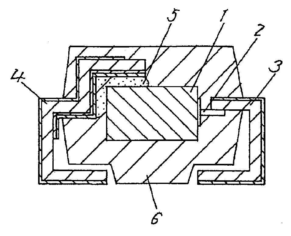
In Fig. 1, capacitor is equipped with capacitor element 1, anode lead wire 2, anode terminal 3, cathode terminal 4, conducting resinl 5 and potting resin 6.Capacitor element 1 has anode bodies and the dielectric oxide film layer that stacks gradually in this anode body surface, solid electrolyte layer and cathode layer (not shown).Capacitor element 1 has anode leader and negative electrode lead division.Cathode terminal 4 is electrically connected with the negative electrode lead division, and anode terminal 3 is electrically connected with anode leader.Anode bodies is that the formed body to the button powder carries out sintering and makes, and is porous matter.The state that potting resin 6 is exposed with an anode terminal 3 and cathode terminal 4 part separately coats junction capacitance device element 1.Potting resin 1 has insulating properties.Anode lead wire 2 as anode leader is connected with anode bodies, the surface that is exposed at anode bodies of this anode lead wire 2.Methods such as the one end employing welding of anode terminal 3 are connected with anode lead wire 2.The other end of anode terminal 3 is exposed at the outside of potting resin 6, and along potting resin 6 bendings.Mode like this, an end of cathode terminal is connected with the cathode layer of capacitor element 1 by conducting resinl 5.Cathode terminal 4 constitutes an external terminal.The other end of cathode terminal 4 is exposed at the outside of potting resin 6, and along potting resin 6 bendings.Constitute like this and outside the connection use another external terminal.
Fig. 2 is vertical view and the cutaway view that forms the lead frame of anode terminal 3 that above-mentioned capacitor uses and cathode terminal 4, and Fig. 2 b is the 2A-2A cutaway view of Fig. 2 a.In Fig. 2, lead frame 11 that is to say that by nickel or Fe-Ni alloy (42 alloy) or copper or copper alloy band plate-like hardwares such as (copper-nickel-tin alloys etc.) formation lead frame 11 is exactly a hardware 11.Anode terminal 3 and cathode terminal 4 are on this lead frame 11.The intermetallic compounds layer that generates as between the tin coating 7 of first coating and this tin coating and the above-mentioned hardware is arranged as first mask of a face of lead frame 11.
If above-mentioned hardware 11 is nickel or Fe-Ni alloy, then intermetallic compounds layer is a tin-nickel; If above-mentioned hardware 11 is copper or copper alloy, then intermetallic compounds layer is tin-copper.The thickness of tin coating 7 is about 4.0~9.0 μ, and the thickness of intermetallic compounds layer is about 0.4~2.0 μ.Above-mentioned first face is equivalent to outer surface one side after anode terminal 3 shown in Figure 1 and cathode terminal 4 bendings, and this first energy soldering is to substrate.Silvering 7 and intermetallic compounds layer are prepared by following operation, promptly directly prepare the operation of tin coating 7 on the surface of hardware without prime coat and make hardware and tin coating 7 between generate the intermetallic compound of tin-nickel or tin-copper and soft heat treatment process that it is carried out.
Second mask as the another side of lead frame 11 has nickel prime coat 8 and preparation the silvering 9 on this prime coat 8 of preparation at metal component surface.The thickness of plating 8 is about 1.0 μ at the bottom of the nickel.Second is equivalent to the side that is connected with capacitor element 1 in Fig. 1.This second is connected with capacitor element 1.So just form element fixed part 10.
Thickness with regard to tin coating is tested the capacitor of such formation.That is: adopt iron-nickel matter alloy as the band plate-like hardware that constitutes lead frame 11 on these capacitors, this alloy uses 42 alloys of 42%Ni-Fe.The tin coating 7 of the no prime coat of all thickness is plated on respectively on this hardware, in atmosphere, they are carried out soft heat then and handle, so that generate the intermetallic compounds layer of tin-nickel between hardware and the tin coating 7 under 500 ℃ the temperature, at various oxygen concentrations.Like this capacitor of experimental example 1~experimental example 20 100 have been made respectively.At 60 ℃, in the gas of 90~95%R.H these capacitors are carried out 240 hours humidity test, again the scolding tin wetability after this humidity test is estimated.The evaluation result of this scolding tin wetability is shown in table 1.The scolding tin wetability is to adopt the ET-7404 scolding tin balancing method of ELAJ method to estimate.Solder(ing) paste uses the RMA type cream of Sn-37Pb.Evaluation temperature is 235 ℃.The judgment standard of scolding tin wetability is, is then to be " zero " below 3.0 seconds the time when the zero crossings time, is then to be " * " more than 3.1 seconds the time when the zero crossings time.
Table 1
| | Sn thickness of coating (μ) | Oxygen concentration (ppm) in the soft heat stove | The scolding tin wetability of humidity test is estimated |
| Experimental example 1 | ????3 | ????50 | ????× |
| Experimental example 2 | ????3 | ????100 | ????× |
| Experimental example 3 | ????3 | ????200 | ????× |
| Experimental example 4 | ????3 | ????250 | ????× |
| Experimental example 5 | ????4 | ????50 | ????○ |
| Experimental example 6 | ????4 | ????100 | ????○ |
| Experimental example 7 | ????4 | ????200 | ????○ |
| Experimental example 8 | ????4 | ????250 | ????× |
| Experimental example 9 | ????5 | ????50 | ????○ |
| Experimental example 10 | ????5 | ????100 | ????○ |
| Experimental example 11 | ????5 | ????200 | ????○ |
| Experimental example 12 | ????5 | ????250 | ????× |
| Experimental example 13 | ????8 | ????50 | ????○ |
| Experimental example 14 | ????8 | ????100 | ????○ |
| Experimental example 15 | ????8 | ????200 | ????○ |
| Experimental example 16 | ????8 | ????250 | ????× |
| Experimental example 17 | ????10 | ????50 | ????○ |
| Experimental example 18 | ????10 | ????100 | ????○ |
| Experimental example 19 | ????10 | ????200 | ????○ |
| Experimental example 20 | ????10 | ????250 | ????× |
As seen from Table 1, when the thickness of tin coating 7 more than 4 μ, then the scolding tin wetability is good.Particularly the oxygen concentration in the soft heat stove is below the 200ppm, more can improve the scolding tin wetability.
Moreover this is that the temperature in the soft heat stove is to make capacitor under the 500 ℃ fixed state of weighing apparatus, but does not limit like this, and the temperature in the soft heat stove is being exactly desirable more than 231.9 ℃ promptly more than the fusing point of tin.And consider mass-produced actual conditions, and according to the purpose that shortens productive temp it will be melted at short notice, this just requires to handle under higher temperature.That is to say that 400 ℃~800 ℃ temperature range is optimum.Present embodiment just is being based on such reason and temperature in the soft heat stove is being set at 500 ℃.
Then, heat-resisting this three's of tack the relation property of again capacitor of said structure having been estimated the tin coating of the thickness of intermetallic compounds layer of material category, tin-nickel of hardware and these capacitors is estimated.That is: materials used is the plate-shape metal member of 30%Ni-Fe alloy (30 alloy), 42%Ni-Fe alloy (42 alloy) and 100%Ni.On each hardware, directly prepare the thick tin coating of 6.0 μ 7 without prime coat.Then, under each temperature of 300 ℃~800 ℃, carry out soft heat and handle, so that generate the tin-nickel intermetallic compound of all thickness between tin coating and the hardware.To the heat-resisting tack of these capacitors evaluation tin coatings, evaluation result is as shown in table 2.Oxygen concentration when in addition, soft heat is handled is 200ppm.The thickness of intermetallic compound is that data with the Auger electron spectroscopy analysis are basic calculation.Aspect the judgment standard of heat-resisting tack, be that the hardware with tin coating and intermetallic compounds layer is curved bending radius is the U font of 0.5mm, in 125 ℃ atmosphere, placed 100 hours, use stereoscope (10 times) to observe the curved surface of tin coating then.Be when the tin coating of bend is not peeled off " zero ", be when having part to peel off " △ ", be when all peeling off " * ".Result of the test is shown in table 2.
Table 2
| The material category of plate-shape metal member | The soft heat treatment temperature (℃) | The thickness of the intermetallic compounds layer of tin-nickel (μ) | The heat-resisting tack of tin coating |
| 30 alloys | ????300 | ????0.1~0.2 | ????× |
| 30 alloys | ????350 | ????0.2~0.3 | ????△ |
| 30 alloys | ????400 | ????0.4~0.6 | ????○ |
| 42 alloys | ????500 | ????0.5~0.7 | ????○ |
| 100% nickel | ????800 | ????1.7~2.0 | ????○ |
As seen from Table 2, when the thickness of the intermetallic compounds layer of tin-nickel more than 0.4 μ, then bend is not peeled off fully, can obtain good heat-resisting tack; When the thickness of intermetallic compounds layer is 0.2~0.3 μ, part then takes place peel off; When the thickness of intermetallic compounds layer is 0.1~0.2 μ, then all peel off.In other words, obtain the heat-resisting tack of very good tin coating, the thickness of the intermetallic compounds layer of tin-nickel will be reached more than 0.4 μ.Moreover concerning hardware, its material uses materials such as nickeliferous 42 many alloys and 100% nickel than using nickeliferous 30 alloys that lack more can obtain good heat-resisting tack.Also have, improve the soft heat treatment temperature and just can obtain the intermetallic compounds layer of thicker and stable tin-nickel.
The result of study of the relation of the thickness of shown in Figure 3 the is silvering 9 of preparation on former electrodes fixed part 10 and the ESR characteristic of capacitor.The ESR characteristic here is meant equivalent series resistance (equivalent series resistance).As seen from Figure 3, when the thickness of silvering 9 more than 0.3 μ, then the ESR value is high, promptly has good ESR characteristic.
Like this, the capacitor of this exemplary embodiments, structure below preparing like this on the hardware that constitutes anode terminal 3 and cathode terminal 4, promptly directly prepare tin coating 7, and between hardware and tin coating 7, generate the intermetallic compounds layer of tin-nickel or tin-copper by it being carried out soft heat handle without prime coat.Do after this manner, just can simplify electroplating processes, can bring into play good scolding tin wetability for a long time again, can obtain to be furnished with the capacitor of the terminal of good heat-resisting tack, can obtain so all capacitors of effects in the hope of reducing cost.
In addition, in this exemplary embodiments, illustrated that capacitor element 1 is that the powder that is embedded with cathode terminal 2 is carried out press molding, and it has been carried out the element that button solid electrolytic capacitor that sintering makes is used.But do not limit so, as the element that capacitor element also can use the solid electrolytic capacitor of valve effect metal forming system to use, this also can obtain same effect.In addition in the present embodiment, as capacitor element, be not subjected to above-mentioned qualification, above-mentioned capacitor element has: play the metal of valve effect, by being formed on the dielectric oxide film on the above-mentioned valve and being configured in the molecular solid electrolyte of high score of the conduction on this dielectric oxide film and being formed on cathode layer on this solid electrolyte.
Also have, also can not use tin coating as the-coating of preparation on anode terminal 3 and cathode terminal 4, and any one tin in the coating such as use Xi-Yin or Sn-Bi, tin-zinc, tin-copper is alloy layer, so also can obtain same effect.
Exemplary embodiments 2
The capacitor of exemplary embodiments 2 is compared with the capacitor of exemplary embodiments 1, and the antianode terminal is different with the formation of the electroplating processes that cathode terminal is implemented, and formation in addition is identical with manufacture method with exemplary embodiments 1.Give identical symbol with exemplary embodiments 1 identical part, and omit its explanation.Below only different parts is illustrated.
Fig. 4 is the structure cutaway view of the button solid electrolytic capacitor of exemplary embodiments 2.Fig. 5 is the cutaway view that forms the lead frame of anode terminal and cathode terminal on this capacitor.In Fig. 4 and Fig. 5, capacitor is equipped with anode terminal 3A and cathode terminal 4A.Anode terminal 3A and cathode terminal 4A each have first and be in second of its back side.First face is can the face of soldering on substrate.Terminal 3A and 4A first, on the surface of hardware, directly prepare tin coating 7 (thickness 4.0~9.0 μ) without prime coat.Then, it is carried out the soft heat processing, thereby between hardware and tin coating 7, generate the intermetallic compounds layer (thickness 0.4~2.0 μ, not shown) of tin-nickel or tin-copper etc.
Anode terminal 3A is to be connected face with capacitor element 1 with cathode terminal 4A second face separately over there.As shown in Figure 5, on second whole, preparation nickel prime coat 8 (thickness 0.3 μ) on the surface of hardware, the part that is connected with capacitor element 1 on this prime coat 8 prepares silvering 9 (thickness 1.0 μ) again.So just form electrode-fixing section 10.
That is to say that in this exemplary embodiments 2, nickel prime coat 8 preparation is at anode terminal 3A and cathode terminal 4A separately on second whole.On the contrary, in above-mentioned exemplary embodiments 1,8 preparations of nickel prime coat are in second part that is connected with capacitor element 1 of cathode terminal.In exemplary embodiments 1 when the front travel that carry out need sheltering when parcel plating is handled and so on.And as this exemplary embodiments 2, the front travel that just need not to shelter and so on when second whole face is carried out electroplating processes so just can be sought the more simplification of manufacturing process.
Exemplary embodiments 3
This exemplary embodiments 3 is compared with above-mentioned exemplary embodiments 2, and the thickness of the tin coating of preparation on anode terminal and cathode terminal is different, and promptly the tin coating of the exposed portions serve of anode terminal and cathode terminal is thin.This exemplary embodiments 3 structure in addition is identical with exemplary embodiments 2 with manufacture method.Give identical symbol with exemplary embodiments 2 identical parts, and omit its explanation.Below only different parts is illustrated.
Fig. 6 is the cutaway view of pith of the button solid electrolytic capacitor structure of exemplary embodiments 3 of the present invention.In Fig. 6, on the face of cathode terminal 4A first (formation is soldered to a side of the solder side on the substrate), on the surface of hardware, directly prepare tin coating 7 (thickness 4.0~9.0 μ) with prime coat.Again it is carried out the soft heat processing, thereby between hardware and tin coating 7, generate the intermetallic compounds layer (thickness 0.4~2.0 μ, not shown) of tin-nickel or tin-copper etc.Not shown equally in the drawings, but on first of anode terminal 3A, prepare too tin coating 7 and intermetallic compounds layer are arranged.
Moreover, on above-mentioned anode terminal 3A and cathode terminal 4A second (side that is connected with capacitor element 1) separately whole, preparation nickel prime coat 8 (thickness 0.3 μ) on the surface of hardware.The part that is connected with capacitor element 1 on this prime coat 8 prepares silvering 9 (thickness 1.0 μ) again, thereby forms electrode-fixing section 10.
In addition, the thickness t of tin coating 7
1In 4.0.~9.0 μ scopes, the packed resin 6 of the part of tin coating 7 is sealed, and another part is exposed at the outside of potting resin 6.The thickness t of this part tin coating 7 that exposes
2Compare thickness t by mechanical treatments such as shot-peenings
1Thin approximately 0.2~1.0 μ.
Fig. 7 is the grinding thickness of expression bead and the relation characteristic figure of leakage current.As seen from Figure 7, work as t
2Being 0.2 μ when above, is that grinding more than 0.2 μ just can make leakage current reduce and stable by stock removal promptly.
So just form: the thickness t that is positioned at this part the anode terminal 3A and the tin coating 7 on the cathode terminal 4A of the outside that is exposed at potting resin 6
2Than thin thickness 0.2~1.0 μ that is positioned at the tin coating 7 on that part of that packed resin 6 seals.Therefore, anode terminal 3A and cathode terminal 4A during along potting resin 6 bendings, just can relaxed the bending stress that this Bending Processing produces.So, just can reduce the leakage current (LC) of one of the key property of capacitor.Particularly since attenuate the outside that forms after the bending be this one side of soldering face, so more can improve above-mentioned effect.
Exemplary embodiments 4
This exemplary embodiments 4 is different with aforementioned typical embodiment 1 for the formation of the electroplating processes that anode terminal and cathode terminal are set up.In addition structure is identical with exemplary embodiments 1 with manufacture method.Give identical symbol with exemplary embodiments 1 identical part, and omit its explanation.Below only different parts is illustrated.
Fig. 8 is the structure cutaway view of the button solid electrolytic capacitor of this exemplary embodiments 4.
In Fig. 8, at anode terminal 3B and cathode terminal 4B first (face of soldering side to the substrate), on the surface of hardware without prime coat directly preparation as the tin coating 7 (thickness 4.0~9.0 μ) of first coating.
Moreover, go up the connecting portion that is connected with capacitor element 1 at cathode terminal 4B second (face that is connected a side with capacitor element 1), preparation nickel prime coat 8 (thickness 0.3 μ) on the surface of hardware.On this prime coat 8, prepare silvering 9 (thickness 1.0 μ) again.And then second of cathode terminal, apart from this connecting portion at least on the position of 0.5mm without prime coat directly preparation as the second tin coating 7a of second coating.
Second face at anode terminal 3B prepares the second tin coating 7a too.It is carried out the soft heat processing, thereby between the hardware and the second tin coating 7a, generate second intermetallic compounds layer (thickness 0.4~2.0 μ, not shown) of tin-nickel or tin-copper etc.So just form electrode-fixing section.Adopt such structure, the electrical characteristics of capacitor are just more stable.
Like this, the capacitor of this exemplary embodiments is owing to the intermetallic compounds layer that generates tin-nickel or tin-copper etc. on the two sides of anode terminal 4A and cathode terminal 4B, so can make electrical characteristics more stable.
Exemplary embodiments 5
The formation and the shape after the bending of the anode terminal of this exemplary embodiments 5 and the electroplating processes of cathode terminal are different with exemplary embodiments 1.In addition structure is identical with exemplary embodiments 1 with manufacture method.Give identical symbol with exemplary embodiments 1 identical part, and omit its explanation.Below only different parts is illustrated.
Fig. 9 is the structure cutaway view of the button solid electrolytic capacitor of exemplary embodiments 5.In Fig. 9, capacitor has anode terminal 3C and cathode terminal 4C.As first of a face of cathode terminal 4C, its part energy soldering is to substrate, and this another part of first is connected with capacitor element 1.That is to say, first of cathode terminal 4C, preparation nickel prime coat 8 (thickness 0.8 μ) on the metal component surface of the connecting portion that is connected with capacitor element 1.On this prime coat 8, prepare silvering 9 (thickness 1.0 μ) again.So just form electrode-fixing section 10.And, at first, having at least on the position in 0.5mm gap apart from this silvering 9, on the surface of hardware, directly prepare tin coating 7 without prime coat.First preparation tin coating 7 at anode terminal 3C.It is carried out the soft heat processing, thereby between hardware and tin coating 7, generate the intermetallic compounds layer (thickness 0.4~2.0 μ, not shown) of tin-nickel or tin-copper etc.The bending shape of anode terminal 3C and cathode terminal 4C is different with aforementioned typical embodiment 1, and other structure is identical with aforementioned typical embodiment 1.
Like this,, just changed the bending shape of anode terminal 3C and cathode terminal 4C, and only an antianode terminal 3C and cathode terminal 4C face is separately implemented electroplating processes according to this exemplary embodiments.Adopt this structure, just unlike above-mentioned exemplary embodiments 1~4, need carry out electroplating processes, thereby simplify manufacturing process more two faces.As a result, can seek to reduce cost.
Exemplary embodiments 6
This exemplary embodiments 6 relates to the manufacture method of used anode terminal of button solid electrolytic capacitor and cathode terminal.
Figure 10 is in the manufacture method of the used anode terminal of capacitor of making this exemplary embodiments 6 and cathode terminal, takes to electroplate earlier the manufacturing procedure picture of back impact style.
In Figure 10, at first shown in Figure 10 a, on the surface of the face (back side among the figure) of nickel or Fe-Ni alloy (42 alloys etc.) or copper or copper alloy band plate-like hardwares (lead frame) 11 such as (copper-nickel-tin alloys etc.), directly prepare the tin coating (not shown) without prime coat.Then it is carried out the soft heat processing, thereby between hardware 11 and tin coating, generate the intermetallic compounds layer of tin-nickel or tin-copper etc.
Then shown in Figure 10 b, prepare nickel prime coat (not shown) in the part that is connected with capacitor element 1 of the another side (front among the figure) of hardware 11, again preparation silvering 9 on this prime coat.So just form electrode-fixing section 10.
Then shown in Figure 10 c, the hardware 11 that will have coating is die-cut into the shape of regulation.
Thereafter shown in Figure 10 d, the hardware 11 of punching established practice setting shape is carried out pressure processing, be bent into the anode terminal 3 and the cathode terminal 4 of regulation shape.Afterwards, coating electrically conductive glue 5 on the electrode-fixing section 10 of the cathode terminal of making like this 4.
After this shown in Figure 10 e, on conducting resinl 5, bear the negative electrode aspect of capacitor element 1, to connect capacitor element.The anode lead wire 2 that adopts method handle such as welding to draw from capacitor element 1 then is connected on the anode terminal 3.Come the wiring capacitance device like this.Thereafter, the nonuseable part on the removal lead frame.
Figure 11 is in the manufacture method of the capacitor anode terminal of making this exemplary embodiments 6 and cathode terminal, takes the manufacturing procedure picture of plating mode after the first punching press.
At first shown in Figure 11 a, prepare the band plate-like hardware (lead frame) 11 of nickel or Fe-Ni alloy (42 alloys etc.) or copper or copper alloy (copper-nickel-tin alloy etc.).
Shown in Figure 11 b, this band plate-like hardware 11 is die-cut into the shape of regulation then.
Then shown in Figure 11 c, on the surface of the face (back side among the figure) of hardware 11, directly prepare the tin coating (not shown) without prime coat.Again it is carried out the soft heat processing, thereby between hardware 11 and tin coating, generate the intermetallic compounds layer of tin-nickel or tin-copper.The part that is connected with capacitor element 1 at the another side (front among the figure) of hardware 11 prepares nickel prime coat (not shown) again.On this prime coat, prepare silvering 9 again.Just form electrode-fixing section 10 like this.So just obtain coating and handle part.
Then shown in Figure 11 d, the electroplating processes part is carried out pressure processing, to make anode terminal 3 and cathode terminal 4.Afterwards, coating electrically conductive glue 5 on the electrode-fixing section 10 of the cathode terminal of making like this 4.
Follow shown in Figure 11 e again, on conducting resinl 5, bear the negative electrode aspect of capacitor element 1, to connect capacitor element.The cathode terminal 2 that adopts method handle such as welding to draw from capacitor element 1 again is connected on the anode terminal 3.Come the wiring capacitance device like this.Thereafter, the nonuseable part on the removal lead frame 11.
The manufacture method of plating mode all is operable after plating back impact style or the first punching press like this, earlier.The use of these manufacture methods is suitably decision after considering various characteristics.
As above-mentioned, the coating that adopts structure of the present invention can simplify terminal is handled, and seeks cost degradation.And terminal can be brought into play good scolding tin wetability for a long time.Moreover terminal has good heat-resisting tack.The result can obtain the good capacitor that so is equipped with entirely of terminal, can obtain especially to pay attention to environment and the capacitor of abandoning environmental pollution material lead.