Take into account these factors; the object of the present invention is to provide a kind of chip transfer device; wherein; with precut and be divided into a plurality of small pieces and be coated with the wafer of a protective tapes can be continuously and automatically transfer on a transfering belt and the annular frame; and described protective tapes can be stripped down, thereby it can be accommodated in the conveyance part.The result, transfer device of the present invention can prevent because of the caused cracked phenomenon of conveyance LED reverse mounting type, cause is carried out caused fracture of conveyance and cracked phenomenon by each conveyance part between each device, and because of from each conveyance part, taking out the cracked phenomenon of caused wafer (small pieces).
The present invention is intended to solve the defective of prior art and achieve the above object.According to the present invention, provide a kind of and one wafer has been adhered to the chip transfer device of an annular frame by a transfering belt, described wafer is divided into a plurality of small pieces and its surface adhesion has a protective tapes, and described chip transfer device comprises:
Thereby one can will be stained with the described wafer of described protective tapes be arranged on the positioning table and can be along the longitudinal, laterally and hand of rotation carry out the position and adjust the detent mechanism of described wafer orientation in a reference position;
One transfering belt installing mechanism, it can be stained with wafer described protective tapes, that be positioned at described reference position with described detent mechanism be arranged on the transfering belt erecting bed and a transfering belt can be adhered to the annular frame that is provided with around the wafer periphery and the back side of described wafer on, thereby can be with described wafer and annular frame bonding each other and become an integral body; And
One protective tapes mechanism for stripping; it can be coated with its back side described transfering belt and become holistic described wafer with described transfering belt installing mechanism and described annular frame and be arranged on the protective tapes stripping table; and an end of peeling off band can be bonded on the end of the described protective tapes that sticks on the described chip back surface; and the described band of peeling off of stretchy, thereby described protective tapes can be stripped down from described wafer surface.
Because this structure, can tell the cut-off rule of the wafer that is cut into small pieces, and can carry out the position adjustment along direction (XY direction) and hand of rotation (θ direction) in length and breadth, thus can be to a reference position with wafer orientation.Therefore, can in the small pieces engagement step, carry out accurate little chip bonding.In addition, can carry out transfer tasks and protective tapes overburden operation continuously, need not to utilize wafer transfer mechanism to carry out.Therefore, can prevent breaking, damage and ftractureing of wafer.
In chip transfer device of the present invention; preferably; described protective tapes is a kind of protective tapes with ultraviolet hardening pressure sensitive adhesives; and described transfer device also comprises a ultraviolet irradiation mechanism, and it can shine with ultraviolet protective tapes before wafer surface strips down with the protective tapes mechanism for stripping to protective tapes.
In the present invention, described ultraviolet irradiation mechanism preferably is provided with to such an extent that can carry out the ultraviolet irradiation operation before transfering belt is adhered to wafer.
The described pressure sensitive adhesives that shines curing can be used as the adhesive agent of protective tapes; and can carry out irradiation by ultraviolet; thereby the bond strength of protective tapes is reduced, can in the protective tapes strip step, easily protective tapes be peeled off from the wafer that is divided into small pieces.
In addition, in chip transfer device of the present invention, preferably, described transfering belt is a kind of transfering belt with ultraviolet hardening pressure sensitive adhesives, and this chip transfer device comprises that also one can be in the ultraviolet irradiation mechanism that wafer and annular frame are shone described transfering belt with ultraviolet after boning each other.
The described pressure sensitive adhesives that shines curing can be used as the adhesive agent of transfering belt, and can carry out irradiation by ultraviolet, picks up bond strength and reduces thereby make, can be in the small pieces adhesion step, and very convenient the picks up small pieces from the surface of transfering belt.
In addition; chip transfer device of the present invention preferably also comprises an accommodating mechanism; described accommodating mechanism is equipped with a containing box that is used for taking in described wafer, and it and described annular frame become an integral body, and with the protective tapes mechanism for stripping protective tapes are stripped down from wafer surface.
In the present invention; preferably; be used in the protective tapes mechanism for stripping peeling off the band be a temperature-sensitive adhesive tape; and construct to such an extent that can be bonded in protective tapes one end that adheres to wafer surface, thereby and the described band of peeling off can be drawn back and described protective tapes can be stripped down from described wafer surface by the end that hot melt will be peeled off band.
By this structure, owing to when peeling off protective tapes, peel off with non-caked transfering belt in annular frame, so can improve the efficient of overburden operation.
In the present invention, chip transfer device preferably also comprises and is used for the device of between each mechanism described wafer of conveyance, described carrying device construct under the situation that can hold at all surfaces with described wafer, the described wafer of conveyance.
Therefore,, just can prevent the local load on the wafer, and then prevent wafer fracture and cracked by hold all surfaces of wafer with suction.
Below in conjunction with accompanying drawing, the form of implementation (embodiment) of chip transfer device of the present invention is described.
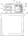
Now see also Fig. 1, mark 10 is total shows chip transfer device of the present invention.Chip transfer device 10 can be divided into the wafer that is stained with a protective tapes on a plurality of small pieces and its to one to be handled (hereinafter; the described wafer that will be divided into a plurality of small pieces is called " wafer W ", and described a plurality of small pieces are fixed into the wafer form with a protective tapes).This wafer W can obtain according to said method.That is, begin to cut along the thickness direction of wafer, from the surface with circuit of a wafer and have given depth, thereby make the bottom of each groove have a cutting pattern until it.Then, a protective tapes is adhered to described wafer surface, and chip back surface is ground to the groove with bottom, thereby wafer is divided into a plurality of small pieces.
By one do not give graphic, after independently the grinding back surface device carries out grinding back surface; utilize carrying arm 12 to make to be coated with protective tapes, move and it be arranged on the wafer transport platform 100 on the pedestal 14 that is loaded on chip transfer device 10 through the wafer W of above-mentioned processing; like this, the protective tapes P side of wafer W has just constituted a downside.Now see also Fig. 2, this transport platform 100 is configured to like this, that is, do not give rotatablely moving of a graphic electrical motor and be delivered to pulley 102 with a belt conveyor, makes ball-screw 104 rotations that link to each other with pulley 102 thus.As a result, the transport platform pedestal 106 that links to each other with ball-screw 104 just can be along guide rail 108 vertical shifting.Because this structure allows to do vertical moving, therefore, transport platform pedestal 106 can carry out synchronous vertical shifting with the vertical shifting of the sorption portion of carrying arm 12.When the wafer W that remains on the absorbed portion (not shown) place of carrying arm 12 by absorption was transported to transport platform pedestal 106, it was damaged to prevent that wafer W from taking place.
The transport platform pedestal 106 of transport platform 100 can be made of a sorption part, the sorption portion 214 of the sorption conveyance part 216 that for example will be described below.
In addition, if not for wafer W is provided with transport platform 100, then can adopt an accommodating container that uses for wafer W be used as one can container is disposed thereon the mounting pedestal.Wafer W through the grinding back surface step is accommodated in the described accommodating container, thereby and takes out wafer W discontinuously and can further handle.
The wafer W that has been moved and has been arranged on the transport platform 100 can be sent to ultraviolet ray (UV) irradiation means 300 by wafer transfer mechanism 200.
Now see also Fig. 4 and Fig. 5, wafer transfer mechanism 200 is configured to like this, promptly, rotatablely moving of the axle drive shaft of driving motor 202 can be passed to S. A. 206 by the driving band 208 on the wheel rim of pulley 204 and pulley 208, described pulley 204 links to each other with axle drive shaft, and pulley 208 is fixed on the S. A. 206.As a result, the carrying arm 210 that links to each other with S. A. 206 just can be as shown in phantom in Figure 4 rotatablely moves as circular arc around S. A. 206 like that.Sorption conveying unit 212 is equipped with in the end of carrying arm 210.The sorption conveyance part 216 that its downside has dish type sorption portion 214 links to each other with the lower end of sorption conveying unit 212 by the spring (not shown). therefore, just can obtain a kind ofly can support the structure that sorption conveying unit 212 is made perpendicular movement, and, can reduce the impact that when sorption keeps, is produced.The sorption part 218 that is made of for example porous ceramics is equipped with in the sorption portion 214 of sorption conveyance part 216.By sorption part 218 is linked to each other with a vacuum source such as the vacuum pump that does not show, can produce a negative pressure, like this, all can be by the sorption of sorption part 218 and maintains in the side of all small pieces of wafer W, thereby can fixed wafer W.Owing to adopt this structure, can prevent that therefore each small pieces of wafer W from taking place to rupture and damage.
Therefore, wafer transfer mechanism 200 is configured to like this, that is, and and by starting drive motor 202, conveying unit 210 can be rotated around S. A. 206, thereby makes the sorption portion 214 of sorption conveyance part 216 just be positioned at the top of the transport platform pedestal 106 of transport platform 100.Like this, the side of all small pieces of wafer W all can maintain by sorptive force by sorption part 218 (sorption liner).When maintaining the sorption maintenance, carrying arm 210 rotates around S. A. 206 with starting drive motor 202, thus can be with the wafer W conveyance to ultraviolet irradiation mechanism 300.
A ultraviolet lampshade 304 is equipped with in ultraviolet irradiation mechanism 300, and described ultraviolet lampshade has the quartz burner 302 that is arranged on wafer transfer arm 210 belows as shown in Figure 4.The ultraviolet ray that emits from quartz burner 302 is under the effect of catadioptre 306 and upwards irradiation.
Just; thereby when carrying arm 210 by start drive motor 202 center on S. A. 206 rotations make wafer W from ultraviolet lamp 300 tops when also conveyance is to detent mechanism 400; with the sorptive force of the sorption portion 214 of the sorption conveyance part 216 of wafer transfer mechanism 200 and the downside of the wafer W that maintains, promptly the protective tapes P side of wafer W is shone by the ultraviolet light that emits from quartz burner 302.
Its objective is; when in the adhesive agent that the ultraviolet hardening pressure sensitive adhesives is used in protective tapes P so that the wafer W that will be divided into a plurality of small pieces with bonding is when maintaining; the bond strength that produces when peeling off protective tapes can be by reducing with the described protective tapes of ultraviolet light irradiation, thereby can easily described protective tapes be stripped down from a plurality of small pieces.
In through ultraviolet irradiation mechanism 300 by the wafer W of ultraviolet light irradiation under the sorption of the sorption portion 214 of the sorption conveyance part 216 of wafer transfer mechanism 200, be the sorption hold mode by conveyance to detent mechanism 400.Wafer W is carried and is arranged on the positioning table 401, so the small pieces side upwards keeps flat.
Now see also Fig. 6 to Fig. 8, detent mechanism 400 comprises: be fixed in the pedestal 14 of chip transfer device 10 and the Y direction guide rail 402 that is provided with along front and rear direction (Y direction) according to apparatus of the present invention and be provided with so that perpendicular to the X-direction guide rail 404 of Y direction guide rail 402 to (X-direction) along right, left according to apparatus of the present invention.And X-direction guide rail 404 is constructed to such an extent that can move on Y direction guide rail 402 along Y direction.Positioning table 401 is installed on the X-direction guide rail 404, and positioning table 401 is constructed to such an extent that can move on X-direction guide rail 404 along X-direction.
The front of Y direction guide rail 402 is equipped with driving motor 406.Driving band 412 be wrapped in driving motor 406 axle drive shaft pulley 408 and be arranged on the pulley of the pulley 410 on the rear end side of Y direction guide rail 402.Therefore, driving band 412 can be with the rotation of driving motor 406 and is moved along X-direction.Therefore, structure is manufactured like this, that is, X-direction guide rail 404 can move along Y direction by the guide (not shown) that is fixed in driving band 412 and links to each other with X-direction guide rail 404 with positioning table 401 disposed thereon.
On the other hand, the left end side of X-direction guide rail 404 is equipped with driving motor 414.Driving band 420 is wrapped in the pulley 416 of driving motor 414 and is arranged on the wheel rim of the pulley 418 on the right-hand member side of X-direction guide rail 404.Therefore, described driving band can be with the rotation of driving motor 414 and is moved along X-direction.Therefore, structure is manufactured like this, that is, positioning table 401 can move along X-direction by the guide (not shown) that is fixed in driving band 420 and links to each other with positioning table 401.
Can be thereby positioning table 401 comprises positioning table framework 422 and is fixed in positioning table framework 422 by bearing 424 around the positioning table base portion 428 of S. A. 426 rotations.Structure construction is become like this, promptly, the rotatablely moving of driving motor 430 that is arranged on the positioning table framework 422 can pass to positioning table base portion 428 by driving band 436, described driving band be wrapped in driving motor 430 transmission shaft pulley 432 and be arranged on the wheel rim of the pulley 434 on the S. A. 426.As a result, positioning table base portion 428 can be around S. A. 426 rotations.
Dish type wafer storage portion 438 is arranged on the upper surface of positioning table base portion 428.Has the porous sorption part 440 that can utilize sorptive force that all surfaces of wafer has been attracted with similar wafer storage portion 438 of aforementioned wafer transfer mechanism 200.Sorption part 440 is linked to each other with a vacuum source such as the vacuum pump (not shown), can make the sorption part have a negative pressure, therefore, all protective tapes sides of wafer W all can be maintained by sorption by sorption part 440, thereby wafer W can be fixed.
With regard to detent mechanism 440 with above-mentioned structure, above ultraviolet irradiation mechanism 300 through the out-of-date wafer W of having used ultraviolet light irradiation already by conveyance to detent mechanism 400.In this conveyance process, wafer W is to be held in the state that is maintained by sorption portion 214 sorptions of the sorption conveyance part 216 of wafer transfer mechanism 200.Wafer W is carried and is arranged in the wafer storage portion 438 of positioning table base portion 428 of positioning table 401, therefore, the side of small pieces upwards keeps flat.So far, just finished the sorption maintenance operation of wafer W.
Owing to keep this state, therefore, utilization is arranged on the image identification camera (not shown) of detent mechanism 400 tops, can be along the wafer cut-off rule that is divided into small pieces of wafer W, carry out position adjustments in longitudinal and transverse direction (XY direction) and hand of rotation (θ direction).As a result, described wafer is positioned at a reference position, so just can carry out correct little chip bonding in the small pieces engagement step.The adjustment of this position can be undertaken by identification is carried out in the position of the directional plane of wafer W or groove.
Just, positioning table 401 is moved along X-direction on X-direction guide rail 404, thereby can determine the X-direction position of described wafer.X-direction guide rail 404 and positioning table 401 disposed thereon are moved on Y direction guide rail 402 along Y direction, thereby can determine the Y direction position of described wafer.Make positioning table base portion 428 around S. A. 426 rotations, thereby can determine the hand of rotation position of described wafer.Like this, described wafer is located on the described reference position.
With the positioning table 401 of detent mechanism 400 and thus the wafer W of location can be by wafer transfer mechanism 500 and conveyance and being arranged on the transfering belt erecting bed 602 of transfering belt installing mechanism 600, and therefore, the small pieces side of wafer W upwards keeps flat.
Now see also Fig. 9 and Figure 10, wafer transfer mechanism 500 is fixed on the pedestal 14 of chip transfer device 10 with carriage 502, and guide rail 504 is housed, thereby can be along X-direction from detent mechanism 400 extends to transfering belt installing mechanism 600.On the next door of guide rail 504, wafer transfer mechanism 500 also has conveyance guide 506.When conveyance guide 506 was driven by a synchronous belt (not shown) that links to each other with electrical motor 505, described conveyance guide can move along guide rail 504.This conveyance guide 506 is equipped with carrying arm 508 at its left end.Carrying arm 508 is provided with sorption conveyance part 510, and sorption conveyance part is constructed to such an extent that can support carrying arm 508 vertical shifting by the spring (not shown), thereby can reduce the impact that produces when sorption keeps.This sorption conveyance part 510 is provided with dish type sorption portion 512 at its downside.The porous sorption part 514 that whole wafer surface can be held also is equipped with in this sorption portion 512, therefore, by applying a negative pressure, all small pieces sides of wafer W can be held.
In having the wafer transfer mechanism 500 of above-mentioned structure, conveyance guide 506 can move along guide rail 504, until it just is positioned at till the top of wafer storage portion 438 of positioning table 401 of detent mechanism 400 (right side of Fig. 9).Then, the negative pressure of the wafer storage portion 438 of cancellation positioning table 401 is with cancellation sorption maintenance effect, and can be with the negative pressure that is arranged on sorption portion 512 places on sorption conveyance part 510 downsides and sorption maintains by the wafer W of positioning table 401 location.And if keep this state, conveyance guide 506 can move along guide rail 504, until till transfering belt installing mechanism 600 (left side of Fig. 9) and wafer W be moved and be arranged on the transfering belt erecting bed 602 of transfering belt installing mechanism 600.
Now see also Fig. 1, transfering belt installing mechanism 600 is equipped with transfering belt erecting bed 602, in its front portion, is provided with the annular frame device 604 of stockpiling and storing, and accommodates a plurality of annular frames in described annular frame is stockpiled and stored device.One of a plurality of annular frame R are deposited on another, and are accommodated in annular frame and stockpile and store in the device 604.The annular frame device 604 of stockpiling and storing can vertically slide along the guide rail (not shown) of vertical setting.
Now see also Fig. 1, annular frame stockpile and store device 604 above, be provided with one from shifting the stockpile and store guide rail 624 of device 604 of adhesive tape erecting bed 602 to annular frame along Y direction.Annular carrying arm 626 is constructed to such an extent that can move along guide rail 624.Annular carrying arm 626 is equipped with one in hollow sorption portion that its leading edge has a hollow liner (not shown).
Therefore, the wafer W of being located by positioning table 401 can move and be arranged on the transfering belt erecting bed 602 of transfering belt installing mechanism 600 with wafer transfer mechanism 500, and like this, the small pieces side of wafer upwards keeps flat.Then, annular carrying arm 626 moves along a guide cylinder, stockpiles and store till the top of device 604 until it is positioned at annular frame.Thereafter, the annular frame device 604 of stockpiling and storing is promoted along guide rail, the annular frame R that is positioned at the top so just can be by annular carrying arm 626 and sorption maintains.Then, stockpile and store device 604 of annular frame is descended, annular carrying arm 626 is moved along guide rail 624, until it be positioned at transfering belt erecting bed 602 directly over till.As a result, annular frame R is just removable and be arranged on around the periphery of the wafer W on the transfering belt erecting bed 602.
Absorbing head 603 is arranged on the inside of transfering belt erecting bed 602, and side thereon is provided with a porous sorption part that can the wafer all surfaces have been attracted with sorption.Therefore, the operation that all side sorptions of the protective tapes P of wafer W are kept can be finished by applying a negative pressure.
Therefore, wafer W and be arranged on annular frame R around the periphery of wafer W on the upper surface of absorbing head 603 sorption and maintain.Then, the transfering belt T that will be in advance precuts according to the shape of annular frame R with transfering belt feed mechanism 650 adheres to the upside of wafer W.
Now see also Figure 11, in transfering belt feed mechanism 650, in advance with precut to determining deviation and adhere to the transfering belt T that strips off liner (release liner) D with the driving of transfering belt feed electrical motor 652 and from uncoiler 654 beginning conveyances and through gap and deflector roll 674 between deflector roll 656, dance roller 658, idler roller 672 and the hold-down roller 660.Release liner D folds back with an acute angle sharp at an exterior region of peel plate 676, thereby transfering belt T can be stripped down from release liner D.Then, release liner D passes through gap and the guide rail 684 between take-up roll 678 and the hold-down roller 680 and is wrapped on the coiler 686.
Do not illustrate though give among the figure, but an adhesive tape detects belting and is arranged on gap and between idler roller 672 and the hold-down roller 660 and passes between the transfering belt of leader of deflector roll 674, like this, by control feed electrical motor 692, each adhesive tape is stopped at given position.
The transfering belt T that will strip down from release liner D in this way by hold-down roller 691 adheres on annular frame R and the wafer W simultaneously.
For the variation with transition zone pad external diameter adapts, each dance roller 658,682 all can vertically move, and its upright position is detected, so that the driving situation of transition zone feed electrical motor 652 and coiler 686 is controlled.
On the other hand, see also Fig. 1, transfering belt erecting bed 602 can be by being arranged on guide rail 690 motions that transfering belt erecting bed 602 in-to-in guides 688 transversely are provided with.Because this structure, transfering belt erecting bed 602 can move towards such direction, that is, make transfering belt erecting bed 602 near or leave that direction of transfering belt feed mechanism 650.
Therefore, now see also Figure 12 (a), transfering belt erecting bed 602 moves along guide rail 690 towards the direction that makes transfering belt erecting bed 602 near peel plate 676.Make the edge portion of annular frame R be positioned at peel plate 676 exterior region near.
By at the exterior region of peel plate 676 with the release liner D acute angle that folds back sharp, transfering belt T can be stripped down from release liner D.Meanwhile, the exterior region of transfering belt T goes to prevent it from following release liner D by means of the way of for example blowing and so on.
Then, see also Figure 12 (b), do not give graphic vertical cylinder by one transfering belt erecting bed 602 is raised up.Then, by pressure roller 691, under the certain pressure effect, the exterior region of transfering belt T is adhered on the annular frame R.
And, seeing also Figure 12 (c), transfering belt erecting bed 602 moves along guide rail 690 towards the direction that transfering belt erecting bed 602 is left be pulled away from peel plate 676.When doing to move like this, by pressure roller 691, transfering belt T adhered to wafer W and the annular frame R that is provided with around wafer W on.As a result, wafer W just becomes an integral body with annular frame R.
Then, see also Fig. 1, annular frame R goes up that can be by the hollow pad 642 of the arm 641 of the pivot arm mechanism 640 that is arranged on transfering belt erecting bed 602 next doors and sorption maintains around the part of the periphery of wafer W.Then, the arm 641 that makes pivot arm mechanism 640 is around S. A. 644 Rotate 180s °, like this, just becomes upwards with the surface of the bonding protective tapes P of wafer W and to keep flat.
Consult Fig. 1 again, the conveyance part 752 of carrying arm mechanism 750 moves along guide rail 754, and described guide rail extends to the center of pivot arm mechanism 640 along X-direction.Maintained by 640 sorptions of pivot arm mechanism and sorption maintains and be transported to this place by the hollow pad 756 of carrying arm mechanism 750 by transfering belt and annular frame R wafer W in aggregates.Then, conveyance part 752 is moved along guide rail 754, thereby wafer W is arranged in the protective tapes stripping table portion 802 of protective tapes mechanism for stripping 800.
Now see also Figure 13 to Figure 15, protective tapes mechanism for stripping 800 comprises: stripping table portion 802, peel off band feed portion 804, as mobile device peel off head 806, and as the heating cutting part 808 of bonding/cutter sweep.
The stripping table 812 that can longitudinally move is equipped with in stripping table portion 802 on track 810, described track is arranged on the pedestal 14 of chip transfer device 10.Driving motor 814 can make stripping table 812 move on track 810 along X-direction by the unitor 822 that links to each other with driving band 820, and described driving band is wrapped on the wheel rim of the pulley 816 of axle drive shaft of described electrical motor and pulley 818.Stripping table 802 surface thereon also is equipped with the porous sorption part 824 that all surfaces of wafer can have been attracted, and like this, by applying a negative pressure, can all surface of wafer W be held through transfering belt T.
Now see also Figure 17, peel off band feed portion 804 and comprise: hold-down roller 825 that can contact with each other under pressure and idler roller 827; Deflector roll 828 and hold-down roller 826.In a bottom of peeling off band feed portion 804, adhesive tape bearing plate 832 is fixed on the ball bush (ball bush) 835 by axle 833.Adhesive tape bearing plate 832 can move along X-direction, and can be by spring 836 along the continuous bias voltage of projection direction (to Figure 17 right-hand).
Peeling off band S winds off and is folded between hold-down roller 826 and the deflector roll 828 from spool 823.Its direction can be changed by deflector roll 828.And stripping tape S is folded between hold-down roller 825 and the idler roller 827, and is delivered to forward on the adhesive tape bearing plate 832, and is pressed on the adhesive tape bearing plate 832 by compactor plate 834.Cutting groove 839 is all the time at a leading section of adhesive tape bearing plate 832.Drive adhesive tape compactor plate 834 so that can be by cylinder body 838 and vertical shifting.Synchronous belt 837 is wrapped on the wheel rim of idler roller 827 and synchronous pulley 831, and pulley 831 can be driven by electrical motor 821 (participation Figure 15) synchronously.Make idler roller 827 towards rotating in the opposite direction, like this, peel off band S and just have at the tensile force (back tension) that produces in the opposite direction with described feed side with the feed side of peeling off band S.
Idler roller 827 is equipped with adhesive tape compactor guide 830 at its rear side (left side of Figure 17), and the band S that peels off that it can prevent to remain on the adhesive tape bearing plate 832 moves backward.
Peeling off band feed portion 804 can move along vertical direction (Z-direction shown in Figure 17).Specifically, see also Figure 13, substrate 803 is arranged on the pedestal 14, peels off band feed portion 804 and moves along Z-direction with being fixed on the cylinder body 805 on the substrate 803.
What one the heat-pesistant thin film that is provided with a temperature-sensitive tack coat or such as pet film itself can be had heat sensitivity peels off band as peeling off band S.
Peel off the arm 842 that head 806 comprises stripping head 840 and supports stripping head 840.Arm 842 also is configured to and can vertically moves with driving motor 847.Stripping head 840 is equipped with chuck 849, and described chuck is made up of upper gripper jaw 846 and following jaw 848, and can be with cylinder body 850 and vertical shifting, thereby can be with chuck 849 opening and closing.In described figure, mark 853 expression adhesive tape detecting sensors.
Now see also Figure 16, temperature booster cutting part 808 is equipped with can be by the temperature booster block 852 of cylinder body 851 vertical shifting.Temperature booster 854 is embedded in the inside of temperature booster block 852, and a lower end of temperature booster block 852 is provided with heater tool 855.
The forward and backward side of temperature booster block 852 is equipped with adhesive tape pressure roller 856.The rear side of temperature booster block 852 also is equipped with adhesive tape compressing member 858, and be equipped with can be by the cutting blade 864 of cylinder body 860 along adhesive tape compressing member 858 side travels.
Figure 17 to Figure 23 shows the protective tapes mechanism for stripping 800 with above-mentioned structure.
Now see also Figure 17, will peel off band S and pull out, until till its arrival cutting groove 839, and stripping table 812 is moved, until its arrives till a certain position of peeling off band feed portion 804 belows.In this state, a back tension can put on by idler roller 827 to be peeled off on the band S.Then, make and peel off head 806 and peel off head 806 and move near the directions of peeling off band feed portion 804 towards making.In the meantime, chuck 849 is to remain on open mode.
Now see also Figure 18, peel off head 806 adhesive tape bearing plate 832 is compressed.Meanwhile, after closed chuck 849, the leading edge of peeling off band S with 853 pairs of adhesive tape detecting sensors detects.Remain between the jaw of chuck 849 peeling off band S, will peel off band compactor plate 834 and raise, peel off the back tension of band S with elimination.
See also Figure 19 again, make and peel off head 806 and peel off head 806 and leave the direction of peeling off band feed portion 804 and move, thereby can pull out peeling off band S towards making.
Then, see also Figure 20, temperature booster cutting part 808 is descended, can compress guide 856 and will peel off band S and compress by peeling off band compressing member 858 and peeling off band like this.Meanwhile,, be used to heat, melt with heat and be with S to be bonded on the protective tapes P of wafer surface peeling off from the temperature booster 854 of temperature booster block 852 by heater tool 855.By cutting blade 864 is moved as Y direction along the groove 862 of peeling off band compressing member 858, will peel off band S and be cut to a given length.Preferably, bonding point is positioned near the edge of wafer W, for example, and at the described edge of distance wafer W in 3 millimeters the scope.
To peel off band feed portion 804 and temperature booster cutting part 808 raises up as shown in Figure 21.Then, make and peel off head 806 and stripping table 812 towards their directions are away from each other moved, as shown in Figure 22.As a result, can the protective tapes P on the described wafer surface be stripped down from described wafer surface by peeling off band S.Preferably, be about 180 ° with peeling off the peel angle of being with S to strip down from wafer W.When described peel angle is 180 ° of left and right sides, can finish described overburden operation and those each small pieces dislocation that is separated that can not make wafer W.
Now see also Figure 23, unclamp and meanwhile carry out air blast from the top by the chuck 849 that will peel off head 806, make through peel off peel off band S and protective tapes P falls in the ash can 870, so that they are taken within it.
With protective tapes mechanism for stripping 800 protective tapes P can be moved and be arranged on the discharge delivery device 900 from the wafer W that described wafer surface strips down by carrying arm mechanism 950.
Now see also Figure 24 and Figure 25, carrying arm member 954 is equipped with in carrying arm mechanism 950, and this carrying arm member 954 can move laterally on guide rail 952.This guide rail 952 extends to the distributing roller portion 902 that discharges delivery device 900 from stripping table 812 beginnings of protective tapes mechanism for stripping 800 along Y direction.Carrying arm member 954 is equipped with sorption cushion member 956 and the sorption portion 958 of its position with the corresponding setting of annular frame R.
Therefore, with regard to the wafer W that protective tapes P is stripped down from the wafer W surface with protective tapes mechanism for stripping 800, the carrying arm member 954 of carrying arm mechanism 950 can move along guide rail 952.Then, by the sorption cushion member 956 of sorption portion 958, maintain being arranged on annular frame R part sorption on protective tapes mechanism for stripping 800 stripping tables 812, that be holistic wafer W with annular frame R.When keeping this sorption hold mode, conveyance part member 954 is moved along guide rail 952, thereby wafer W is moved and be arranged in the distributing roller portion 902 that discharges delivery device 900.
Now see also Fig. 1, discharge delivery device 900 left and right side guide 902 on a pair of pedestal 14 that is fixed on chip transfer device 10 is housed.Each inside face of this offside guide 902 all has a roller part (roller part), and described roller part is made up of a plurality of roller (not shown)s that are provided with constant space.Annular frame R part contacts with each roller part, thereby can avoid producing breakage because of wafer contacts with roller.
Movable cylinder 908 is arranged on the rear of each roller part.Movable cylinder 908 can be done laterally to slide under certain directional tagging by guide rod 910.The pushing piece (not shown) that is fixed on a upside of movable cylinder 908 can promote the wafer W that moves and be arranged on each roller part according to the moving of movable cylinder 908 towards the front side.As a result, wafer W can be accommodated in the containing box 1002 of the shedding mechanism 1000 that is positioned on the described front side.
Above-mentioned shedding mechanism 1000 is constructed to such an extent that energy is for vertical movement, thereby containing box 1002 can be positioned at and discharge the corresponding position of height of each roller part of delivery device 900.
The present invention should not be subjected to the restriction of previous embodiment.Various improvement can also be arranged, for example, ultraviolet irradiation mechanism can be arranged on the downstream of transfering belt installing mechanism.
Can also use an adhesive tape that is coated with a kind of ultraviolet hardening pressure sensitive adhesives as transfering belt T, and can with one with ultraviolet irradiation mechanism 300 similar, to being used to wafer W is adhered to the place ahead or the rear that ultraviolet irradiation mechanism that the transfering belt T on the annular frame R shines is arranged on described discharge delivery device with ultraviolet.
Adopt chip transfer device of the present invention, can carry out that direction (XY direction) and hand of rotation (θ direction) are carried out the position adjustment in length and breadth along the small pieces wafer cut-off rule of wafer W.Therefore, can be with described wafer orientation in a reference position, thus can in the small pieces engagement step, carry out correct little chip bonding, and can avoid small pieces impaired.And, can be continuously and automatically position operation, transfer tasks and protective tapes overburden operation, and need not carry out conveyance by the conveyance part, thus can avoid wafer fracture, damage and cracked.
In addition,, therefore can prevent that wafer is subjected to local load, thereby can prevent wafer fracture and cracked effectively because the present invention can hold all surfaces of described wafer.