Summary of the invention
, during the comb poles put down in writing, electrode area is added man-hour in being used in the 2001-237375 patent gazette that Japan announces calendar year 2001, the zone that sustains damage is a lot.And with rectangular electrode relatively comb poles is little for the capacitance of electrode plane size, be difficult to make the electric capacity of high-capacitance.Produce because the scattered problem that causes the scattered grade of capacitance of the processing dimension of broach again.
And in multilayered wiring structure, then processing dimension is very fine because if there is lower floor, and pattern is also very intensive, is very difficult so will make the large-area electric capacity of high capacitance when forming this electric capacity in lower floor.
Again, in the structure of in the 2002-33453 patent gazette that Japan announced in 2002, putting down in writing, though solved above-mentioned problem, but form semiconductor chip and multilayer wired after, because must append all newly, increase considerably such problem so exist process number in order to form the required operation of electric capacity.
The present invention proposes in view of the above problems, the objective of the invention is with easy manufacture method in the semiconductor device that possesses MIM electric capacity, forms the MIM electric capacity of high power capacity high reliability.
Semiconductor device of the present invention is the semiconductor device with MIM electric capacity, have and be arranged on the on-chip interlayer dielectric of semiconductor bulk and imbed above-mentioned interlayer dielectric, distribution with above-mentioned semiconductor chip conducting, above-mentioned MIM electric capacity has the 1st and the 2nd electrode that is made of metal and the capacitor insulating film that is made of dielectric, above-mentioned the 1st electrode is imbedded in the above-mentioned interlayer dielectric, above-mentioned capacitor insulating film is arranged on above-mentioned the 1st electrode, above-mentioned the 2nd electrode is the metal level that is provided with by above-mentioned capacitor insulating film and above-mentioned the 1st electrode contraposition, on the part of above-mentioned distribution, expose and pad electrode is set, on above-mentioned the 2nd electrode, be provided with the another part of above-mentioned distribution and the connecting line of the 2nd electrode electrical connection, above-mentioned pad electrode is formed by identical metal film with above-mentioned connecting line.
Best above-mentioned capacitor insulating film is the film with function of the metal diffusing that prevents to constitute at least one side in the above-mentioned the 1st and the 2nd electrode.
In certain preferential example, above-mentioned capacitor insulating film is the film that is made of silicon nitride.
The manufacture method of semiconductor device of the present invention is included in the operation a that forms interlayer dielectric on the semiconductor chip, on above-mentioned interlayer dielectric, form the operation b of many ditches and a plurality of through holes, by metal being imbedded above-mentioned many ditches and above-mentioned a plurality of through hole, the operation c of the 1st electrode of formation conducting MIM electric capacity and the distribution of above-mentioned semiconductor chip, on above-mentioned the 1st electrode, form the operation d of the capacitor insulating film that constitutes by dielectric, with by on above-mentioned capacitor insulating film, metal level being set, form the operation e of the 2nd electrode of above-mentioned MIM electric capacity, after above-mentioned operation e, remove the operation f of the part of above-mentioned capacitor insulating film, the connecting line that is connected with a part that forms above-mentioned the 2nd electrode and above-mentioned distribution, operation g with the pad electrode that is connected with another part of above-mentioned distribution, above-mentioned operation d is at above-mentioned the 1st electrode, form the operation of above-mentioned capacitor insulating film on the surface of above-mentioned distribution and the part of exposing above-mentioned interlayer dielectric, above-mentioned operation e is the operation that forms above-mentioned the 2nd electrode after on the above-mentioned capacitor insulating film above-mentioned metal level being set by this metal level of etching.
In certain preferential example, above-mentioned operation g is the operation that is formed above-mentioned connecting line and above-mentioned pad electrode by identical metal film.
Best above-mentioned capacitor insulating film is the film with function of the metal diffusing that prevents to constitute at least one side in the above-mentioned the 1st and the 2nd electrode.
In certain preferential example, above-mentioned capacitor insulating film is the film that is made of silicon nitride.
In the present invention as described above, in the manufacturing of semiconductor device that possesses the MIM electric capacity that lamination metal electrode-dielectric film in turn-metal electrode forms and semiconductor device, with the wiring layer of the rarer top section of lower floor Comparing patterns density in form capacitance electrode, can increase electrode area with the situation comparison that in lower floor's wiring layer, forms MIM electric capacity.Further, by simultaneously with the same metal level of distribution on form capacitance electrode, manufacturing process is changed jointly, with the situation that in the superiors, forms the MIM capacitance electrode relatively, only need be used to form electric capacity minority to append operation just passable.
Embodiment
Semiconductor device according to the present invention has MIM electric capacity, has to be arranged on the interlayer dielectric on the semiconductor chip and to imbed above-mentioned interlayer dielectric, with the distribution of above-mentioned semiconductor chip conducting.And, MIM electric capacity has the 1st and the 2nd electrode that is made of metal and the capacitor insulating film that is made of dielectric, above-mentioned the 1st electrode is imbedded in the above-mentioned interlayer dielectric, above-mentioned capacitor insulating film is arranged on above-mentioned the 1st electrode, and above-mentioned the 2nd electrode is the metal level that is provided with by above-mentioned capacitor insulating film and above-mentioned the 1st electrode contraposition.Thereby (in same operation) forms distribution in the wiring layer be arranged on the semiconductor chip and the 1st electrode of MIM electric capacity simultaneously, can reduce the process number of the manufacturing process of semiconductor device, can reduce manufacturing cost.Here MIM electric capacity refers to the electric capacity that metal-insulator-metal type constitutes.
In certain example, because expose on the part of above-mentioned distribution and pad electrode is set, above-mentioned pad electrode is made of the above-mentioned metal level identical with above-mentioned the 2nd electrode, so partly form MIM electric capacity in the multilayer wired the superiors.Relatively Wiring pattern density is rarer because multilayer wired the superiors part is with underclad portion, so can easily form the big capacitance electrode of area, the capacitance of electric capacity is increased.Because form the 2nd electrode of pad electrode and MIM electric capacity simultaneously,, can reduce manufacturing cost so can reduce the process number of the manufacturing process of semiconductor device again.Here pad electrode refers to be used for connecting semiconductor device and outer member or distributing board and to be arranged on and uses electrode being connected of semiconductor device, is signal input and output and the part of accepting source current.Usually pad electrode is to be made of the metal that exposes on the surface of semiconductor device (Al etc.).
Best above-mentioned capacitor insulating film is the film with function of the metal diffusing that prevents to constitute at least one side in the above-mentioned the 1st and the 2nd electrode.For example, in the situation that a side electrode is made of Cu, when capacitor insulating film select by the group that forms from SiN, SiON, SiC and SiOC at least a when constituting, because capacitor insulating film also has the function that prevents the Cu diffusion, so do not need to form in addition the film that prevents the Cu diffusion, can suppress the increase of process number, reduce manufacturing cost.Again; because in order not injure the surface of semiconductor device; inner in order not allow moisture invade again; generally on semiconductor device the most surperficial, form the SiN film as diaphragm; so when capacitor insulating film is made of SiN; can suppress to invade, again can enough and existing manufacturing process identical materials device suppress the increase of manufacturing cost from the moisture of outside, so just more satisfactory.
Below, we describe example of the present invention with reference to the accompanying drawings in detail.For the purpose of simplifying the description, represent to have the inscape of identical function in fact with identical with reference to label in the accompanying drawing below.
(example 1)
We are simultaneously with reference to Fig. 1, Fig. 2, Fig. 5, and one side illustrates example 1 of the present invention.
Fig. 1 is the pattern sectional view of the semiconductor device in this example.Fig. 2 (a)~(d) is the pattern sectional view of the manufacturing process of the semiconductor device in this example of expression.Again, Fig. 5 is the program diagram of the manufacturing process of the semiconductor device in this example of expression.
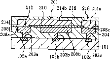
As shown in Figure 1, the semiconductor device of this example has semiconductor chip 101, is arranged on interlayer dielectric 204 above it and a part and imbeds remainder in the interlayer dielectric 204 and be arranged on MIM electric capacity 201 on the interlayer dielectric 204.Semiconductor chip 101 for example is the substrate that forms transistor (not drawing among the figure), other electron component (not drawing among the figure) and distribution 102a, 102b, 102c etc. on silicon chip, or at the substrate that forms the wiring layer (metal wiring is set) more than 1 layer on this silicon chip on interlayer dielectric.In interlayer dielectric 204, imbed by copper and constitute distribution 208a, 208c and the 1st electrode 208b again.These distributions 208a, 208c and the 1st electrode 208b are by distribution 102a, the 102c102b conducting of through hole 203a, 203c, 203b and semiconductor chip 101.MIM electric capacity 201 is by imbedding the 1st electrode 208b in the interlayer dielectric 204, being arranged on the capacitor insulating film 210 on the 1st electrode 208b and the 2nd electrode 214b that is made of Al that is arranged on the capacitor insulating film 210 constitutes.The 2nd electrode 214b is connected with distribution 208a by the Al that imbeds the contact hole 212 that is arranged in the capacitor insulating film 210.On distribution 208c, form the pad electrode 214a that constitutes by the metal level identical with the 2nd electrode 214b again.Further, on whole beyond on the pad electrode 214a of the superiors, the diaphragm 218 that is made of SiN is set.Pad electrode 214a exposes from the opening portion 216 that is arranged on the diaphragm 218.
If according to semiconductor device as described above, then, can enough minority operations form large-area MIM electric capacity 201 by on the metal level that forms distribution 208a, 208c and pad electrode 214a, forming MIM electric capacity 201.
Secondly, we illustrate the manufacture method of semiconductor device in this example with Fig. 2 (a)~Fig. 2 (d) and Fig. 5.
Shown in Fig. 2 (a), on semiconductor chip 101, form interlayer dielectric 204 (S110, operation (a)).And on the interlayer dielectric 204 that forms, form distribution ditch 206a, 206c, the 1st electrode with ditch 206b and through hole 205a, 205c, 205b (S120, operation (b)).
Secondly, shown in Fig. 2 (b), in order to imbed the Cu layer in ditch 206b and through hole 205a, 205c, 205b and 208 and pile up back (S130) at distribution ditch 206a, 206c, the 1st electrode with galvanoplastic, (Chemical Mechanical Polishing (chemico-mechanical polishing) method is ground (S140), forms distribution 208a, the 208c of the state in the interlayer dielectric 204 of imbedding, as the 1st electrode 208b of the lower electrode of MIM electric capacity 201 and through hole 203a, 203c, 203b with CMP.S130 and S140 are operation (c).
Then, shown in Fig. 2 (c), on the surface of interlayer dielectric 204, distribution 208a, 208c and the 1st electrode 208b that behind CMP (S140), is exposing, form by having as dielectric capactive film of MIM electric capacity 201 and preventing the capacitor insulating film 210 (S150, operation (d)) that the SiN of the film function of Cu diffusion constitutes with the CVD method.And, by dry etching, on the capacitor insulating film on distribution 208a, the 208c 210, form connecting hole 212 (S160).
After this, on capacitor insulating film 210, form the metal level 214 (S170) that constitutes by Al with sputtering method.After this, with dry etching (S180), form the 2nd electrode 214b (operation (e)) opposed to each other by capacitor insulating film 210 and the 1st electrode 208b.In addition, the 2nd electrode 214b is connected with the distribution 208a of lower floor by the Al that is filled in the connecting hole 212.Again, use dry etching (S180) simultaneously, form pad electrode 214a with forming the 2nd electrode 214b.
Secondly, shown in Fig. 2 (d), on the 2nd electrode 214b and pad electrode 214a, form the diaphragm 218 that constitutes by SiN, form opening portion 216 in the diaphragm 218 on pad electrode 214a.
If manufacture method according to semiconductor device as described above, then because can in the formation operation (operation (c), operation (e)) of distribution 208a, 208c and pad electrode 214a, form MIM electric capacity 201 simultaneously, so can not need to append the new process relevant with forming MIM electric capacity 201.Again,, do not need to form in addition the film that prevents the Cu diffusion, can reduce process number by form capacitor insulating film 210 by SiN.Further, with the Ta of the capacitor insulating film that is generally used for MIM electric capacity
2O
5Difference is because SiN has remarkable moisture-proof, so capacitor insulating film 210 can play the effect as the diaphragm of the upper layer part of semiconductor device.Again, because generally form the SiN film as diaphragm on the most surperficial semi-conductive, thus by using the film that constitutes by SiN to make capacitor insulating film, can intactly use existing material apparatus, thus the increase of manufacturing cost can be suppressed.
(example 2)
We are simultaneously with reference to Fig. 3, Fig. 4, Fig. 6, and one side illustrates example 2 of the present invention.In addition, because this example is identical with example 1 in fact from the part of interlayer dielectric below 204, so we partly omit the explanation to this part.
Fig. 3 is the pattern sectional view of the semiconductor device in this example.Fig. 4 (a)~Fig. 4 (d) is the pattern sectional view of the manufacturing process of the semiconductor device in this example of expression.Again, Fig. 6 is the program diagram of the manufacturing process of the semiconductor device in this example of expression.
As shown in Figure 3, the semiconductor device of this example has semiconductor chip 101, is arranged on interlayer dielectric 204 above it and a part and imbeds remainder in the interlayer dielectric 204 and be arranged on MIM electric capacity 241 on the interlayer dielectric 204.Again, imbed distribution 208a, the 208c and the 1st electrode 208b that are made of copper on interlayer dielectric 204, they are by through hole 203a, 203c, 203b and semiconductor chip 101 conductings.MIM electric capacity 241 is by imbedding the 1st electrode 208b in the interlayer dielectric 204, being arranged on the capacitor insulating film 210 on the 1st electrode 208b and the 2nd electrode 214b that is made of Al that is arranged on the capacitor insulating film 210 constitutes.By being arranged on the connecting line 224a on the 2nd electrode 214b, the 2nd electrode 214b is connected with distribution 208a.Here, connecting hole 222a part is connected with distribution 208a connecting line 224a on the capacitor insulating film 210 by being arranged on.On distribution 208c, form the pad electrode 224b that constitutes by the metal level 224 identical with connecting line 224a again.Further, on it, on whole beyond on the pad electrode 224b diaphragm 218 is set.Pad electrode 224b exposes from the opening portion 226 that is arranged on the diaphragm 218.
The semiconductor device of this example also by form the 1st electrode 208b of MIM electric capacity 241 on the metal level that forms distribution 208a, 208c, can enough minority operations form large-area MIM electric capacity 201.
Secondly, we illustrate the manufacture method of semiconductor device in this example with Fig. 4 (a)~Fig. 4 (d) and Fig. 6.
Shown in Fig. 4 (a), on semiconductor chip 101, form interlayer dielectric 204 (S210, operation (a)).And on the interlayer dielectric 204 that forms, form distribution ditch 206a, 206c, the 1st electrode with ditch 206b and through hole 205a, 205c, 205b (S220, operation (b)).
Secondly, shown in Fig. 4 (b), in order to imbed the Cu layer in ditch 206b and through hole 205a, 205c, 205b and to pile up back (S230) at distribution ditch 206a, 206c, the 1st electrode with galvanoplastic, (Chemical Mechanical Polishing (chemico-mechanical polishing) method is ground (S240), forms distribution 208a, the 208c of the state in the interlayer dielectric 204 of imbedding, as the 1st electrode 208b of the lower electrode of MIM electric capacity 241 and through hole 203a, 203c, 203b with CMP.S230 and S240 are operation (c).
Then, on the surface of interlayer dielectric 204, distribution 208a, 208c and the 1st electrode 208b that behind CMP (S240), is exposing, form by having as dielectric capactive film of MIM electric capacity 241 and preventing the capacitor insulating film 210 (S250, operation (d)) that the SiN of the film function of Cu diffusion constitutes with the CVD method.
And, shown in Fig. 4 (c), on capacitor insulating film 210, form Al metal level (S260) by sputtering method.And form the 2nd electrode 214b (S270, operation (e)) opposed to each other by capacitor insulating film 210 and the 1st electrode 208b as upper electrode with dry etching.On it, form dielectric film 220 (S280).
After this, shown in Fig. 4 (d),, form connecting line 224a and opening portion (connecting hole) 222a, 22b, 222c (S290) by dielectric film 220 and capacitor insulating film 210 are carried out dry etching.And, for electrode electrically connected 214b forms metal film (be connected and use metal level) 224 (S300) that are made of Al with distribution 208a.Further, form connecting line 224a and pad electrode 224b (S310) by this metal film 224 being carried out etching.Pad electrode 224b is electrically connected with distribution 208c at opening portion 222c.After this, on semiconductor chip, form the diaphragm 218 that constitutes by SiN, opening portion 226 is set on pad electrode 224b exposes pad electrode 224b.
If manufacture method according to semiconductor device as described above, then because can be the formation operation from distribution 208a, 208c to pad electrode 224b (operation (c), operation (e)), form distribution 208a, 208c and pad electrode 224b simultaneously, so can not need to append the new process relevant with forming MIM electric capacity 241.Again,, do not need to form in addition the film that prevents the Cu diffusion, can reduce process number by form capacitor insulating film 210 by SiN.Further, with the Ta of the capacitor insulating film that is generally used for MIM electric capacity
2O
5Difference is because SiN has remarkable moisture-proof, so capacitor insulating film 210 can play the effect as the diaphragm of the upper layer part of semiconductor device.Again,,, existing material apparatus can be intactly used, the increase of manufacturing cost can be suppressed so constitute film by SiN and make capacitor insulating film by using because generally form the SiN film as diaphragm on the most surperficial semi-conductive.
Further, the semiconductor device of this example, because form capacitor insulating film 210, operation without other forms metal film (constituting the metal film of the 2nd electrode 214b) immediately thereon in intact state, so capacitor insulating film 210 can not be subjected to corroding the influence with etching process.Promptly, when in order to connect the 2nd electrode 214b and distribution 208b and to be connected pad electrode 224b and distribution 208c and on capacitor insulating film 210, to form opening portion 222a, 222c, can be subjected to corroding influence with etching process by the part of the 1st electrode 208b in the capacitor insulating film 210 and the 2nd electrode 214b clamping.Thereby, can intactly keep the thickness and the membrane property of the capacitor insulating film 210 that forms, as design load, form the capacitance and the characteristic of MIM electric capacity 241.Again, the capacitance of MIM electric capacity 241 and characteristic scattered can be suppressed to very little.
In addition, at step S260, the metal level or the metal compound layer that form on capacitor insulating film 210 also can be Ti, TiN or Ti/TiN.Thereby the 2nd electrode 214b also can be the electrode of any formation among Ti, TiN or the Ti/TiN.
Above example is an example, the invention is not restricted to these examples.The metal that constitutes the electrode of distribution and MIM electric capacity also can be metal, for example silver and the alloy beyond Cu and the Al.The material that constitutes interlayer dielectric and dielectric film also can be silica and the such materials such as silica that contain fluorine.The structure of MIM electric capacity also can be to play the such structure of electric capacity function.
As described above, in the semiconductor device and manufacture method thereof of this example, can enough minority operations make MIM electric capacity, be useful as the semiconductor device with MIM electric capacity (for example, DRAM and system LSI etc.).