CN1212536C - Electroluminescence panel - Google Patents
Electroluminescence panel Download PDFInfo
- Publication number
- CN1212536C CN1212536C CNB021246939A CN02124693A CN1212536C CN 1212536 C CN1212536 C CN 1212536C CN B021246939 A CNB021246939 A CN B021246939A CN 02124693 A CN02124693 A CN 02124693A CN 1212536 C CN1212536 C CN 1212536C
- Authority
- CN
- China
- Prior art keywords
- switch
- panel according
- gate
- switches
- source
- Prior art date
- Legal status (The legal status is an assumption and is not a legal conclusion. Google has not performed a legal analysis and makes no representation as to the accuracy of the status listed.)
- Expired - Lifetime
Links
Images


Classifications
-
- G—PHYSICS
- G09—EDUCATION; CRYPTOGRAPHY; DISPLAY; ADVERTISING; SEALS
- G09G—ARRANGEMENTS OR CIRCUITS FOR CONTROL OF INDICATING DEVICES USING STATIC MEANS TO PRESENT VARIABLE INFORMATION
- G09G3/00—Control arrangements or circuits, of interest only in connection with visual indicators other than cathode-ray tubes
- G09G3/20—Control arrangements or circuits, of interest only in connection with visual indicators other than cathode-ray tubes for presentation of an assembly of a number of characters, e.g. a page, by composing the assembly by combination of individual elements arranged in a matrix no fixed position being assigned to or needed to be assigned to the individual characters or partial characters
- G09G3/22—Control arrangements or circuits, of interest only in connection with visual indicators other than cathode-ray tubes for presentation of an assembly of a number of characters, e.g. a page, by composing the assembly by combination of individual elements arranged in a matrix no fixed position being assigned to or needed to be assigned to the individual characters or partial characters using controlled light sources
- G09G3/30—Control arrangements or circuits, of interest only in connection with visual indicators other than cathode-ray tubes for presentation of an assembly of a number of characters, e.g. a page, by composing the assembly by combination of individual elements arranged in a matrix no fixed position being assigned to or needed to be assigned to the individual characters or partial characters using controlled light sources using electroluminescent panels
- G09G3/32—Control arrangements or circuits, of interest only in connection with visual indicators other than cathode-ray tubes for presentation of an assembly of a number of characters, e.g. a page, by composing the assembly by combination of individual elements arranged in a matrix no fixed position being assigned to or needed to be assigned to the individual characters or partial characters using controlled light sources using electroluminescent panels semiconductive, e.g. using light-emitting diodes [LED]
- G09G3/3208—Control arrangements or circuits, of interest only in connection with visual indicators other than cathode-ray tubes for presentation of an assembly of a number of characters, e.g. a page, by composing the assembly by combination of individual elements arranged in a matrix no fixed position being assigned to or needed to be assigned to the individual characters or partial characters using controlled light sources using electroluminescent panels semiconductive, e.g. using light-emitting diodes [LED] organic, e.g. using organic light-emitting diodes [OLED]
- G09G3/3225—Control arrangements or circuits, of interest only in connection with visual indicators other than cathode-ray tubes for presentation of an assembly of a number of characters, e.g. a page, by composing the assembly by combination of individual elements arranged in a matrix no fixed position being assigned to or needed to be assigned to the individual characters or partial characters using controlled light sources using electroluminescent panels semiconductive, e.g. using light-emitting diodes [LED] organic, e.g. using organic light-emitting diodes [OLED] using an active matrix
- G09G3/3233—Control arrangements or circuits, of interest only in connection with visual indicators other than cathode-ray tubes for presentation of an assembly of a number of characters, e.g. a page, by composing the assembly by combination of individual elements arranged in a matrix no fixed position being assigned to or needed to be assigned to the individual characters or partial characters using controlled light sources using electroluminescent panels semiconductive, e.g. using light-emitting diodes [LED] organic, e.g. using organic light-emitting diodes [OLED] using an active matrix with pixel circuitry controlling the current through the light-emitting element
- G09G3/3241—Control arrangements or circuits, of interest only in connection with visual indicators other than cathode-ray tubes for presentation of an assembly of a number of characters, e.g. a page, by composing the assembly by combination of individual elements arranged in a matrix no fixed position being assigned to or needed to be assigned to the individual characters or partial characters using controlled light sources using electroluminescent panels semiconductive, e.g. using light-emitting diodes [LED] organic, e.g. using organic light-emitting diodes [OLED] using an active matrix with pixel circuitry controlling the current through the light-emitting element the current through the light-emitting element being set using a data current provided by the data driver, e.g. by using a two-transistor current mirror
-
- H—ELECTRICITY
- H10—SEMICONDUCTOR DEVICES; ELECTRIC SOLID-STATE DEVICES NOT OTHERWISE PROVIDED FOR
- H10D—INORGANIC ELECTRIC SEMICONDUCTOR DEVICES
- H10D86/00—Integrated devices formed in or on insulating or conducting substrates, e.g. formed in silicon-on-insulator [SOI] substrates or on stainless steel or glass substrates
- H10D86/40—Integrated devices formed in or on insulating or conducting substrates, e.g. formed in silicon-on-insulator [SOI] substrates or on stainless steel or glass substrates characterised by multiple TFTs
- H10D86/421—Integrated devices formed in or on insulating or conducting substrates, e.g. formed in silicon-on-insulator [SOI] substrates or on stainless steel or glass substrates characterised by multiple TFTs having a particular composition, shape or crystalline structure of the active layer
- H10D86/425—Integrated devices formed in or on insulating or conducting substrates, e.g. formed in silicon-on-insulator [SOI] substrates or on stainless steel or glass substrates characterised by multiple TFTs having a particular composition, shape or crystalline structure of the active layer having different crystal properties in different TFTs or within an individual TFT
-
- H—ELECTRICITY
- H10—SEMICONDUCTOR DEVICES; ELECTRIC SOLID-STATE DEVICES NOT OTHERWISE PROVIDED FOR
- H10D—INORGANIC ELECTRIC SEMICONDUCTOR DEVICES
- H10D86/00—Integrated devices formed in or on insulating or conducting substrates, e.g. formed in silicon-on-insulator [SOI] substrates or on stainless steel or glass substrates
- H10D86/40—Integrated devices formed in or on insulating or conducting substrates, e.g. formed in silicon-on-insulator [SOI] substrates or on stainless steel or glass substrates characterised by multiple TFTs
- H10D86/431—Integrated devices formed in or on insulating or conducting substrates, e.g. formed in silicon-on-insulator [SOI] substrates or on stainless steel or glass substrates characterised by multiple TFTs having different compositions, shapes, layouts or thicknesses of gate insulators in different TFTs
-
- H—ELECTRICITY
- H10—SEMICONDUCTOR DEVICES; ELECTRIC SOLID-STATE DEVICES NOT OTHERWISE PROVIDED FOR
- H10D—INORGANIC ELECTRIC SEMICONDUCTOR DEVICES
- H10D86/00—Integrated devices formed in or on insulating or conducting substrates, e.g. formed in silicon-on-insulator [SOI] substrates or on stainless steel or glass substrates
- H10D86/40—Integrated devices formed in or on insulating or conducting substrates, e.g. formed in silicon-on-insulator [SOI] substrates or on stainless steel or glass substrates characterised by multiple TFTs
- H10D86/60—Integrated devices formed in or on insulating or conducting substrates, e.g. formed in silicon-on-insulator [SOI] substrates or on stainless steel or glass substrates characterised by multiple TFTs wherein the TFTs are in active matrices
-
- G—PHYSICS
- G09—EDUCATION; CRYPTOGRAPHY; DISPLAY; ADVERTISING; SEALS
- G09G—ARRANGEMENTS OR CIRCUITS FOR CONTROL OF INDICATING DEVICES USING STATIC MEANS TO PRESENT VARIABLE INFORMATION
- G09G2300/00—Aspects of the constitution of display devices
- G09G2300/08—Active matrix structure, i.e. with use of active elements, inclusive of non-linear two terminal elements, in the pixels together with light emitting or modulating elements
- G09G2300/0809—Several active elements per pixel in active matrix panels
- G09G2300/0842—Several active elements per pixel in active matrix panels forming a memory circuit, e.g. a dynamic memory with one capacitor
-
- G—PHYSICS
- G09—EDUCATION; CRYPTOGRAPHY; DISPLAY; ADVERTISING; SEALS
- G09G—ARRANGEMENTS OR CIRCUITS FOR CONTROL OF INDICATING DEVICES USING STATIC MEANS TO PRESENT VARIABLE INFORMATION
- G09G2320/00—Control of display operating conditions
- G09G2320/02—Improving the quality of display appearance
- G09G2320/0219—Reducing feedthrough effects in active matrix panels, i.e. voltage changes on the scan electrode influencing the pixel voltage due to capacitive coupling
Landscapes
- Engineering & Computer Science (AREA)
- Physics & Mathematics (AREA)
- Computer Hardware Design (AREA)
- General Physics & Mathematics (AREA)
- Theoretical Computer Science (AREA)
- Electroluminescent Light Sources (AREA)
- Control Of Indicators Other Than Cathode Ray Tubes (AREA)
Abstract
一种能够改善画面质量的电发光屏板。在该屏板中,第一和第二开关响应通过栅极线提供的选通信号向电容器施加数据线上的信号。第一和第二开关的阈值电压设定成彼此不同。由此就可以避免反冲现象,并能最大限度地减小泄漏电流,从而改善了画面质量。
An electroluminescence panel capable of improving picture quality. In the panel, the first and second switches apply a signal on the data line to the capacitor in response to a gate signal supplied through the gate line. Threshold voltages of the first and second switches are set to be different from each other. As a result, the kickback phenomenon can be avoided, and the leakage current can be minimized, thereby improving picture quality.
Description
本申请要求2001年6月22日申请的韩国专利申请第2001-35662号的权益,因而,为达到所有目的而将该申请在此如同其已在此处全文引述的那样作为参考文献加以结合。This application claims the benefit of Korean Patent Application No. 2001-35662 filed June 22, 2001, which application is hereby incorporated by reference for all purposes as if fully incorporated herein.
技术领域technical field
本发明涉及一种电发光显示器(ELD),更具体地说,是涉及一种能够改善画面质量的电发光屏板。The present invention relates to an electroluminescence display (ELD), and more particularly relates to an electroluminescence panel capable of improving picture quality.
背景技术Background technique
近来,业界已经开发了各种能够消除那些与阴极射线管(CRT)有关的缺点,且重量轻和体积小的平板显示器装置。这类平板显示器装置通常包括:液晶显示器(LCD)、场发射显示器(FED)、等离子显示屏板(PDP)、和电发光(EL)屏板等。Recently, the industry has developed various flat panel display devices that can eliminate the disadvantages associated with cathode ray tubes (CRTs) and that are light in weight and small in size. Such flat panel display devices generally include liquid crystal displays (LCDs), field emission displays (FEDs), plasma display panels (PDPs), and electroluminescence (EL) panels, among others.
为提高平板显示装置的显示质量和提供具有大型显示屏的平板显示器,现已积极地进行了大量的研究。这种显示装置中的EL屏板是自发射装置。EL屏板利用诸如电子和空穴等载流子激励荧光物质显示视频图象。EL屏板的优点在于,可以使用低直流电压驱动,且响应速度快。A great deal of research has been actively conducted to improve the display quality of flat panel display devices and to provide flat panel displays with large display screens. The EL panel in this display device is a self-emitting device. The EL panel uses carriers such as electrons and holes to excite fluorescent substances to display video images. The advantage of the EL panel is that it can be driven with a low DC voltage and has a fast response.
正如图1所示,这种EL屏板包括:以彼此交叉方式设置的栅极线GL和数据线DL、以及在栅极线GL和数据线DL之间的交叉点上设置的象元108。当栅极线GL上起动一个选通信号时,驱动每个象元108,由此产生与数据线DL上的象素信号电流量相对应的光。As shown in FIG. 1, this EL panel includes gate lines GL and data lines DL arranged to cross each other, and pixels 108 arranged at intersections between the gate lines GL and data lines DL. When a gate signal is activated on the gate line GL, each pixel 108 is driven, thereby generating light corresponding to the amount of pixel signal current on the data line DL.
另外,EL屏板104包括:与数据线DL相连的电流驱动器106。每个电流驱动器106响应象素信号,控制电流从象元108经数据线DL流到自身内,由此向每个象元108施加了象素信号。电流驱动器106使电子充电电流流入象元108。随象素信号变化的电流信号借助于电流驱动器106流入象元108。In addition, the EL panel 104 includes a current driver 106 connected to the data line DL. Each current driver 106 responds to the pixel signal by controlling the flow of current from the pixel 108 to itself via the data line DL, thereby applying the pixel signal to each pixel 108 . Current driver 106 flows electron charging current into pixel 108 . A current signal varying with the pixel signal flows into the pixel 108 by means of the current driver 106 .
EL屏板104的栅极线GL与栅驱动器100相连,而电流驱动器106与数据驱动器102相连。栅驱动器100顺序地驱动栅极线GL。数据驱动器102向电流驱动器106施加一根线的象素电压信号。每个电流驱动器106将来自数据驱动器102的象素电压信号转换成反向象素电流信号,并将转换后的象素电流信号施加至象元108。换句话说,电流驱动器106可控制在从象元108通过数据线D的电流流路上的电流量,由此提高了象元108上的最大电流量和与灰度级对应的电流量的差别。结果,EL屏板104能够显示灰度画面。The gate line GL of the EL panel 104 is connected to the gate driver 100 , and the current driver 106 is connected to the data driver 102 . The gate driver 100 sequentially drives the gate lines GL. The data driver 102 applies a pixel voltage signal for one line to the current driver 106 . Each current driver 106 converts the pixel voltage signal from the data driver 102 into an inverted pixel current signal, and applies the converted pixel current signal to the pixel 108 . In other words, the current driver 106 can control the amount of current on the current path from the pixel 108 through the data line D, thereby increasing the difference between the maximum current amount on the pixel 108 and the amount of current corresponding to the gray scale. As a result, the EL panel 104 can display a gray scale picture.
参照图2,象元108包括:与第一低压线FVL相连的EL单元(ELC)和连在EL单元(ELC)与数据线DL之间的EL单元驱动电路110。第一低压线FVL能够与接地电压源GND相连,或能与产生负电压的第一低压源相连。在栅极线GL上起动控制信号的时段内,EL单元驱动电路110向EL单元(ELC)施加一正向电流信号,该信号随数据线DL上的反向电流量变化。为此,EL单元驱动电路110包括:在EL单元(ELC)、第一节点N1和电源电压线VDDL间连接成电流反射镜的第三和第四PMOS TFT Q3和Q4,以及与第二节点N2和电源电压线VDDL相连的电容器C,所述的第二节点N2与第三和第四PMOS TFT Q3和Q4的栅电极共连。Referring to FIG. 2, the pixel 108 includes: an EL unit (ELC) connected to the first low voltage line FVL and an EL unit driving circuit 110 connected between the EL unit (ELC) and the data line DL. The first low voltage line FVL can be connected to the ground voltage source GND, or can be connected to the first low voltage source generating a negative voltage. During the period in which the control signal is activated on the gate line GL, the EL cell driving circuit 110 applies a forward current signal to the EL cell (ELC), which varies with the amount of reverse current on the data line DL. To this end, the EL unit driving circuit 110 includes: the third and fourth PMOS TFTs Q3 and Q4 connected as current mirrors between the EL unit (ELC), the first node N1 and the power supply voltage line VDDL, and the second node N2 The capacitor C connected to the power supply voltage line VDDL, the second node N2 is commonly connected to the gate electrodes of the third and fourth PMOS TFTs Q3 and Q4.
当电源电压线VDDL与数据线DL相连时,电容器C充入数据线DL上的信号电流,并向第三和第四PMOS TFT Q3和Q4的栅电极施加充入的信号电流。第三PMOS TFT Q3由电容器C中充入的信号电流启动,从而将电源电压线VDDL上的电源电压VDD施加至EL单元(ELC)。与此同时,第三PMOSTFT Q3根据电容器C中充入的信号电流量而改变其沟道宽度,从而可以控制从电源电压线VDDL耦合到EL单元(ELC)的电流量。然后,EL单元(ELC)发出与从电源电压线VDDL经第三PMOS TFT Q3施加的电流量相对应的光。第四PMOS TFT Q4也控制从电源电压线VDDL流到数据线DL上的电流,由此决定经第三PMOS TFT Q3流入EL单元(ELC)的电流量。When the power supply voltage line VDDL is connected to the data line DL, the capacitor C charges the signal current on the data line DL, and applies the charged signal current to the gate electrodes of the third and fourth PMOS TFTs Q3 and Q4. The third PMOS TFT Q3 is activated by the signal current charged in the capacitor C, thereby applying the power supply voltage VDD on the power supply voltage line VDDL to the EL cell (ELC). At the same time, the third PMOSTFT Q3 changes its channel width according to the amount of signal current charged in the capacitor C, so that the amount of current coupled from the power supply voltage line VDDL to the EL cell (ELC) can be controlled. Then, the EL cell (ELC) emits light corresponding to the amount of current applied from the power supply voltage line VDDL via the third PMOS TFT Q3. The fourth PMOS TFT Q4 also controls the current flowing from the power supply voltage line VDDL to the data line DL, thereby determining the amount of current flowing into the EL cell (ELC) through the third PMOS TFT Q3.
另外,EL单元驱动电路110还包括:第一和第二PMOS TFT Q1和Q2,它们共同响应栅极线GL上的选通信号。在从栅极线GL施加低逻辑选通信号的时段内使第一PMOS TFT Q1接通,于是将与第一节点N1相连的第一PMOSTFT Q1的源极与数据线DL相连。换句话说,第一PMOS TFT Q1扮演响应低逻辑选通信号形成从电源电压线VDDL经第四PMOS晶体管Q4、第一节点N1和其自身延伸到数据线DL的电流通路的角色。第二PMOS TFT Q2也在低逻辑选通信号由栅极线GL向其栅电极施加的时段内接通,由此通过第二节点N2和与电容器C的一个端子相连的第一节点N1将第三和第四PMOS TFT Q3和Q4的栅电极与数据线DL连接起来。换句话说,在栅极线GL上的选通信号保持在低逻辑态的时段内接通第一和第二PMOS TFT Q1和Q2,以将数据线DL与电源电压线VDDL以及第二节点N2相连,由此充入一个与数据线DL中流动的电流量相对应的电荷量(或信号电流)。In addition, the EL unit driving circuit 110 further includes: first and second PMOS TFTs Q1 and Q2, which jointly respond to the gate signal on the gate line GL. The first PMOS TFT Q1 is turned on during a period in which a low logic gate signal is applied from the gate line GL, thus connecting the source of the first PMOS TFT Q1 connected to the first node N1 to the data line DL. In other words, the first PMOS TFT Q1 plays a role of forming a current path extending from the power supply voltage line VDDL to the data line DL through the fourth PMOS transistor Q4, the first node N1, and itself in response to the low logic gate signal. The second PMOS TFT Q2 is also turned on during the period when the low logic gate signal is applied to its gate electrode by the gate line GL, thereby connecting the second node N1 through the second node N2 and the first node N1 connected to one terminal of the capacitor C. Gate electrodes of the third and fourth PMOS TFTs Q3 and Q4 are connected to the data line DL. In other words, the first and second PMOS TFTs Q1 and Q2 are turned on during the period in which the gate signal on the gate line GL is kept in a low logic state to connect the data line DL to the power voltage line VDDL and the second node N2 are connected to each other, thereby charging a charge amount (or signal current) corresponding to the amount of current flowing in the data line DL.
当选通信号从低逻辑态变为高逻辑态时,接通该EL单元驱动电路110的第一PMOS TFT Q1,同时接通具有相同阈值电压的第二PMOS TFT Q2。于是会产生反冲(kick-back)现象,即其中充入电容器C的电荷量会在选通信号的下降边缘处泄漏。结果,EL单元(ELC)不能精确地产生与数据线DL上的电流量相对应的光,于是引起了画面劣化或失真。When the strobe signal changes from a low logic state to a high logic state, the first PMOS TFT Q1 of the EL unit driving circuit 110 is turned on, and the second PMOS TFT Q2 with the same threshold voltage is turned on at the same time. Then, a kick-back phenomenon occurs, that is, the charge amount charged in the capacitor C leaks at the falling edge of the gate signal. As a result, the EL cell (ELC) cannot accurately generate light corresponding to the amount of current on the data line DL, thus causing picture degradation or distortion.
发明内容Contents of the invention
于是,本发明涉及这样一种电发光屏板,其基本上能避免由于相关技术的局限和缺点导致的一个或多个问题。Accordingly, the present invention is directed to an electroluminescent panel that substantially obviates one or more of the problems due to limitations and disadvantages of the related art.
本发明的优点是提供一种能够改善画面质量的电发光屏板。The advantage of the present invention is to provide an electroluminescence panel capable of improving picture quality.
将在下面的描述中阐述本发明的其他特征和优点,由这些描述会使其变得更明了,或者可通过实践本发明来学到这些特征和优点。通过书面描述和权利要求以及所附附图中具体指出的结构能够实现并得到本发明的目的和其他优点。Additional features and advantages of the invention will be set forth in the description which follows, and will be apparent from the description, or may be learned by practice of the invention. The objectives and other advantages of the invention will be realized and attained by the structure particularly pointed out in the written description and claims hereof as well as the appended drawings.
正如具体例举的和广义描述的那样,为了实现依照本发明目的的这些和其他优点,根据本发明一个实施例的电发光屏板包括:多条栅极线;多条与栅极线交叉的数据线;多个设置在栅极线与数据线之间交叉点上的电发光单元;多个用于从数据线充入信号的电容器;连接在电发光单元和电容器之间的第三开关;与第三开关相连形成电流反射镜的第四开关;以及用于响应通过栅极线提供的选通信号而向电容器施加数据线上的信号的第一和第二开关,所述第一开关的阈值电压设定成低于第二开关的阈值电压。在电发光屏板中,第一开关具有与栅极线相连的栅极端子、与数据线相连的源极端子和与第二开关的源极端子相连的漏极端子。As specifically exemplified and broadly described, in order to achieve these and other advantages according to the object of the present invention, an electroluminescence panel according to one embodiment of the present invention includes: a plurality of grid lines; data line; a plurality of electroluminescence units arranged at intersections between the gate line and the data line; a plurality of capacitors for charging signals from the data lines; a third switch connected between the electroluminescence units and the capacitor; a fourth switch connected to the third switch to form a current mirror; and first and second switches for applying a signal on the data line to the capacitor in response to a gate signal provided through the gate line, the first switch The threshold voltage is set lower than the threshold voltage of the second switch. In the EL panel, the first switch has a gate terminal connected to the gate line, a source terminal connected to the data line, and a drain terminal connected to the source terminal of the second switch.
第二开关具有与栅极线相连的栅极端子、与第一开关的漏极端子相连的源极端子和与电容器相连的漏极端子。The second switch has a gate terminal connected to the gate line, a source terminal connected to the drain terminal of the first switch, and a drain terminal connected to the capacitor.
第一开关的阈值电压和第二开关的阈值电压之间的差值约大于0.5V。The difference between the threshold voltage of the first switch and the threshold voltage of the second switch is greater than about 0.5V.
在电发光屏板中,第三开关用于响应电容器中充入的信号电流向电发光单元施加数据线上的信号;以及第四开关用于控制施加给每个电发光单元的电流。第一到第四开关中的每一个都包括沟道极性相同的薄膜晶体管。In the electro-luminescence panel, the third switch is used to apply the signal on the data line to the electro-luminescence unit in response to the signal current charged in the capacitor; and the fourth switch is used to control the current applied to each electro-luminescence unit. Each of the first to fourth switches includes thin film transistors having the same channel polarity.
第一和第二开关包括沟道极性彼此不同的薄膜晶体管,而第三和第四开关包括沟道极性相同的薄膜晶体管。The first and second switches include thin film transistors whose channel polarities are different from each other, and the third and fourth switches include thin film transistors whose channel polarities are the same.
第二开关的栅极绝缘膜厚度大于第一开关的栅极绝缘膜厚度。The gate insulating film thickness of the second switch is greater than the gate insulating film thickness of the first switch.
第二开关的保护层厚度要大于第一开关的保护层厚度。The thickness of the protection layer of the second switch is greater than the thickness of the protection layer of the first switch.
第二开关的中间层绝缘膜厚度要大于第一开关中间层绝缘膜的厚度。The thickness of the interlayer insulating film of the second switch is greater than the thickness of the interlayer insulating film of the first switch.
第二开关的栅电极具有单层结构,而第一开关的栅电极具有多层结构。The gate electrode of the second switch has a single-layer structure, and the gate electrode of the first switch has a multi-layer structure.
第二开关的源极和漏极具有单层结构,而第一开关的源极和漏极具有多层结构。The source and drain of the second switch have a single-layer structure, while the source and drain of the first switch have a multi-layer structure.
第二开关的源极和漏极由与第一开关的材料不同的材料制成。The source and drain of the second switch are made of a material different from that of the first switch.
第二开关的半导体层由与第一开关的半导体层材料不同的材料制成。The semiconductor layer of the second switch is made of a material different from that of the semiconductor layer of the first switch.
注入第二开关半导体层的离子浓度设定成高于注入第一开关半导体层的离子浓度。The concentration of ions injected into the second switching semiconductor layer is set higher than the concentration of ions injected into the first switching semiconductor layer.
第二开关的半导体层包括氢杂质。The semiconductor layer of the second switch includes hydrogen impurities.
第二开关的半导体层经受利用等离子体进行的表面处理。The semiconductor layer of the second switch is subjected to surface treatment with plasma.
第一开关下基板的结晶方向与第二开关的结晶方向不同。The crystallographic direction of the lower substrate of the first switch is different from that of the second switch.
第二开关的栅电极是由与第一开关栅电极材料不同的材料制成的。The gate electrode of the second switch is made of a material different from that of the gate electrode of the first switch.
需要理解的是,前面的一般性描述和下面的详细描述都是示范性和说明性的,意欲提供对所要求保护的本发明作进一步的说明。It is to be understood that both the foregoing general description and the following detailed description are exemplary and explanatory and are intended to provide further explanation of the invention as claimed.
附图的简要说明Brief description of the drawings
将用以提供对本发明进一步理解的附图结合进来构成本说明书的一部分,这些附图用于说明本发明的实施例,并连同说明一起用于解释本发明的原理。The accompanying drawings, which are included to provide a further understanding of the invention and are incorporated in and constitute a part of this specification, illustrate embodiments of the invention and together with the description serve to explain the principle of the invention.
在附图中:In the attached picture:
图1是表示传统电发光屏板结构的示意性方框图;Fig. 1 is a schematic block diagram showing the structure of a conventional electroluminescence panel;
图2是图1所示象元的详尽电路图;Fig. 2 is a detailed circuit diagram of the pixel shown in Fig. 1;
图3是依照本发明实施例的电发光屏板的象元的详尽电路图;3 is a detailed circuit diagram of a pixel of an electroluminescent panel according to an embodiment of the present invention;
图4是表示图1所示象元的另一开关示例的详尽电路图;Fig. 4 is a detailed circuit diagram showing another switch example of the pixel shown in Fig. 1;
图5是图3所示第一和第二开关的缓冲绝缘层截面图;Fig. 5 is a cross-sectional view of buffer insulating layers of the first and second switches shown in Fig. 3;
图6是图5所示缓冲绝缘层的详尽视图;Fig. 6 is a detailed view of the buffer insulating layer shown in Fig. 5;
图7是图3所示第一和第二开关的有源层截面图;7 is a cross-sectional view of the active layer of the first and second switches shown in FIG. 3;
图8是图3所示第一和第二开关的栅电极和栅极线的截面图;8 is a cross-sectional view of gate electrodes and gate lines of the first and second switches shown in FIG. 3;
图9是表示图3所示第一和第二开关上离子注入过程的截面图;Fig. 9 is a cross-sectional view showing the ion implantation process on the first and second switches shown in Fig. 3;
图10是图3所示第一和第二开关的中间层绝缘膜的截面图;Fig. 10 is a sectional view of interlayer insulating films of first and second switches shown in Fig. 3;
图11是图3所示第一和第二开关的源极和漏极的截面图;11 is a cross-sectional view of the source and drain of the first and second switches shown in FIG. 3;
图12是图3所示第一和第二开关的保护层截面图;以及12 is a cross-sectional view of the protective layer of the first and second switches shown in FIG. 3; and
图13是图3所示第一和第二开关的象素电极的截面图。FIG. 13 is a cross-sectional view of pixel electrodes of the first and second switches shown in FIG. 3. Referring to FIG.
具体实施方式Detailed ways
现在将对本发明的实施例作详尽参引,这些实施例的例子示于附图中。Reference will now be made in detail to embodiments of the invention, examples of which are illustrated in the accompanying drawings.
参照图3,其示出了依照本发明实施例的EL单元驱动电路。Referring to FIG. 3, it shows an EL unit driving circuit according to an embodiment of the present invention.
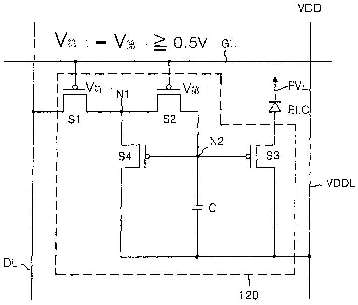
EL单元驱动电路120包括:以在EL单元(ELC)、第一节点N1和电源电压线VDDL中形成电流反射镜的方式连接的第三和第四开关S3和S4;连接在第二节点N2和电源电压线VDDL之间的电容器C,所述的第二节点N2与第三和第四开关S3和S4的栅电极共连;与第一节点N1和栅极线GL相连的第二开关S2;连接在第一节点N1和数据线DL之间的第一开关S1。在此,第一到第四开关中的每一个都由PMOS型TFT制成。The EL unit driving circuit 120 includes: third and fourth switches S3 and S4 connected in such a manner as to form a current mirror in the EL unit (ELC), the first node N1, and the power supply voltage line VDDL; A capacitor C between the power supply voltage lines VDDL, the second node N2 is commonly connected to the gate electrodes of the third and fourth switches S3 and S4; the second switch S2 is connected to the first node N1 and the gate line GL; The first switch S1 is connected between the first node N1 and the data line DL. Here, each of the first to fourth switches is made of a PMOS type TFT.
当电源电压线VDDL与数据线DL相连时,将数据线DL上的信号电流充入电容器C,并将所充入的信号电流共同送入第三和第四开关S3和S4的栅电极。通过电容器C中充入的信号电流接通第三开关S3,由此将电源电压线VDDL上的电源电压VDD施加到EL单元(ELC)。与此同时,第三开关S3根据电容器C中充入的信号电流量而改变其沟道宽度,从而可以控制由电源电压线VDDL耦合到EL单元(ELC)的电流量。然后,EL单元(ELC)发出与由电源电压线VDDL经第三开关S3施加的电流量相对应的光。第四开关S4也控制从电源电压线VDDL流入数据线DL的电流,由此确定经第三开关S3流入EL单元(ELC)的电流量。When the power voltage line VDDL is connected to the data line DL, the signal current on the data line DL is charged into the capacitor C, and the charged signal current is jointly sent to the gate electrodes of the third and fourth switches S3 and S4. The third switch S3 is turned on by the signal current charged in the capacitor C, thereby applying the power supply voltage VDD on the power supply voltage line VDDL to the EL cell (ELC). At the same time, the third switch S3 changes its channel width according to the amount of signal current charged in the capacitor C, so that the amount of current coupled to the EL cell (ELC) from the power supply voltage line VDDL can be controlled. Then, the EL cell (ELC) emits light corresponding to the amount of current applied from the power supply voltage line VDDL via the third switch S3. The fourth switch S4 also controls the current flowing from the power voltage line VDDL into the data line DL, thereby determining the amount of current flowing into the EL cell (ELC) through the third switch S3.
在从栅极线GL施加低逻辑选通信号的时段内接通第一开关S1,从而将与第一节点N1相连的第一开关S1的源极连接到数据线DL上。换句话说,第一开关S1扮演着响应低逻辑选通信号形成从电源电压线VDDL经第四开关S4、第一节点N1和自身延伸到数据线DL的电流流路的角色。在将来自栅极线GL的低逻辑选通信号送入其栅电极的时段内还接通第二开关S2,由此通过第二节点N2和与电容器C的一个端子连接的第一节点N1将第三和第四开关S3和S4的栅电极与数据线DL相接。换句话说,在栅极线GL上的选通信号保持低逻辑状态的时段内接通第一和第二开关S1和S2,以便将数据线DL与电源电压VDDL以及第二节点N2相连,从而向电容器C充入与数据线DL中流动的电流量相对应的电荷量(或信号电流)。The first switch S1 is turned on during a period in which a low logic gate signal is applied from the gate line GL, thereby connecting the source of the first switch S1 connected to the first node N1 to the data line DL. In other words, the first switch S1 plays a role of forming a current flow path extending from the power voltage line VDDL to the data line DL through the fourth switch S4, the first node N1 and itself in response to the low logic gate signal. The second switch S2 is also turned on during the period in which a low logic gate signal from the gate line GL is fed into its gate electrode, whereby the first node N1 connected to one terminal of the capacitor C through the second node N2 will Gate electrodes of the third and fourth switches S3 and S4 are connected to the data line DL. In other words, the first and second switches S1 and S2 are turned on during a period in which the gate signal on the gate line GL maintains a low logic state, so as to connect the data line DL to the power supply voltage VDDL and the second node N2, thereby The capacitor C is charged with an amount of charge (or signal current) corresponding to the amount of current flowing in the data line DL.
该单元驱动电路120有差别地设定第一和第二开关S1和S2的阈值电压V第一和V第二。也就是说,可通过下面将要提到的制造方法将第一开关S1的阈值电压V第一设定成低于第二开关S2的阈值电压V第二。最理想的条件是将第二开关S2的阈值电压V第二与第一开关S1的阈值电压V第一之间的差值(V第二-V第 一)设定为约0.5V以上。当选通信号从低逻辑态变到高逻辑态时,第一开关S1会在第二开关S2之后断开。于是,电容器C中充入的电荷量就不会在选通信号的下降边缘泄漏。其结果是,EL单元(ELC)能够准确地发出与数据线DL上的电流量相对应的光,从而显示出与EL屏板的视频信号(或图像信号)相对应的画面,而没有任何劣化或失真。The cell driving circuit 120 differentially sets the threshold voltages Vfirst and Vsecond of the first and second switches S1 and S2. That is, the threshold voltage Vfirst of the first switch S1 may be set lower than the threshold voltage Vsecond of the second switch S2 through a manufacturing method to be mentioned below. The most ideal condition is to set the difference (Vsecond- Vfirst ) between the threshold voltage Vsecond of the second switch S2 and the threshold voltage Vfirst of the first switch S1 at about 0.5V or more. When the strobe signal changes from a low logic state to a high logic state, the first switch S1 is turned off after the second switch S2. Thus, the charge amount charged in the capacitor C does not leak at the falling edge of the gate signal. As a result, the EL cell (ELC) can accurately emit light corresponding to the amount of current on the data line DL, thereby displaying a picture corresponding to the video signal (or image signal) of the EL panel without any deterioration or distortion.
参照图4,依照本发明另一个实施例的EL单元驱动电路120包括:以在EL单元(ELC)、第一节点N1和接地电压GND中形成电流反射镜(current mirror)的方式连接的第三和第四开关S3和S4;连接在第二节点和电源电压线VDDL之间的电容器C,所述的第二节点与第三和第四开关S3和S4的栅电极共连;与第一节点N1和栅极线GL相连的第二开关S2;以及连接在第一节点N1和数据线DL之间的第一开关S1。在此,第一到第四开关S1到S4中的每一个都由NMOS型TFT制成。Referring to FIG. 4, an EL unit driving circuit 120 according to another embodiment of the present invention includes: a third node connected in a manner of forming a current mirror among the EL unit (ELC), the first node N1, and the ground voltage GND. and the fourth switch S3 and S4; a capacitor C connected between the second node and the power supply voltage line VDDL, the second node is commonly connected with the gate electrodes of the third and fourth switches S3 and S4; and the first node the second switch S2 connected between N1 and the gate line GL; and the first switch S1 connected between the first node N1 and the data line DL. Here, each of the first to fourth switches S1 to S4 is made of an NMOS type TFT.
当接地电压GND与数据线DL相连时,将数据线DL上的信号电流充入电容器C,并将所充入的信号电流共同施加到第三和第四开关S3和S4的栅电极。通过电容器C中充入的信号电流接通第三开关S3,由此向EL单元(ELC)施加接地电压GND。与此同时,第三开关S3根据电容器C中充入的信号电流量而改变其沟道宽度,从而控制从接地电压GND耦合到EL单元(ELC)的电流量。然后,EL单元(ELC)产生与从接地电压GND经开关S3施加的电流量相应的光。第四开关S4也控制从电源电压线VDDL流入数据线DL的电流,从而确定经第三开关S3流入EL单元(ELC)的电流量。When the ground voltage GND is connected to the data line DL, the signal current on the data line DL is charged into the capacitor C, and the charged signal current is commonly applied to the gate electrodes of the third and fourth switches S3 and S4. The third switch S3 is turned on by the signal current charged in the capacitor C, thereby applying the ground voltage GND to the EL cell (ELC). At the same time, the third switch S3 changes its channel width according to the amount of signal current charged in the capacitor C, thereby controlling the amount of current coupled from the ground voltage GND to the EL cell (ELC). Then, the EL cell (ELC) generates light corresponding to the amount of current applied from the ground voltage GND via the switch S3. The fourth switch S4 also controls the current flowing from the power voltage line VDDL into the data line DL, thereby determining the amount of current flowing into the EL cell (ELC) through the third switch S3.
在从栅极线GL施加高逻辑选通信号的时段内接通第一开关S1,由此将与第一节点N1相连的第一开关S1的源极与数据线DL相连。也就是说,第一开关S1扮演着响应低逻辑选通信号形成从电源电压线VDDL经第四开关S4、第一节点N1和自身延伸到数据线DL的电流通路的角色。在将来自栅极线GL的高逻辑选通信号施加到其栅电极的时段内还接通第二开关S2,从而通过第二节点和与电容器C的一个端子相连的第一节点N1将第三和第四开关S3和S4的栅电极与数据线DL相连。也就是说,在栅极线GL上的选通信号保持在高逻辑态的时段内接通第一和第二开关S1和S2,以将数据线DL与接地电压线GND以及第二节点N2相连,由此在电容器C中充入了与数据线DL中流动的电流量相对应的电荷量(或信号电流)。The first switch S1 is turned on during a period in which a high logic gate signal is applied from the gate line GL, thereby connecting the source of the first switch S1 connected to the first node N1 to the data line DL. That is, the first switch S1 plays a role of forming a current path extending from the power voltage line VDDL to the data line DL through the fourth switch S4, the first node N1 and itself in response to the low logic gate signal. The second switch S2 is also turned on during the period in which a high logic gate signal from the gate line GL is applied to its gate electrode, thereby connecting the third switch S2 through the second node and the first node N1 connected to one terminal of the capacitor C. Gate electrodes of the and fourth switches S3 and S4 are connected to the data line DL. That is, the first and second switches S1 and S2 are turned on during a period in which the gate signal on the gate line GL remains in a high logic state to connect the data line DL to the ground voltage line GND and the second node N2. , thereby charging the capacitor C with an amount of charge (or signal current) corresponding to the amount of current flowing in the data line DL.
该单元驱动电路120有差别地设定第一和第二开关S1和S2的阈值电压V第一和V第二。换句话说,通过下面将要提到的制造方法将第一开关S1的阈值电压V第一设定成低于第二开关S2的阈值电压V第二。最理想的状态是将第二开关S2的阈值电压V第二与第一开关S1的阈值电压V第一之间的差值大设定成约0.5V以上。当选通信号从低逻辑态变到高逻辑态时,第一开关S1后于第二开关S2断开。由此,电容器C中充入的电荷量不会在选通信号的下降边缘处泄漏。结果,EL单元(ELC)能够精确地产生与数据线DL上的电流量相对应的光,从而能显示出与EL屏板的视频信号(或图像信号)相对应的画面,而不会存在任何劣化或失真。The cell driving circuit 120 differentially sets the threshold voltages Vfirst and Vsecond of the first and second switches S1 and S2. In other words, the threshold voltage Vfirst of the first switch S1 is set lower than the threshold voltage Vsecond of the second switch S2 by a manufacturing method to be mentioned below. Ideally, the difference between the threshold voltage Vsecond of the second switch S2 and the threshold voltage Vfirst of the first switch S1 is set to be greater than about 0.5V. When the strobe signal changes from a low logic state to a high logic state, the first switch S1 is turned off later than the second switch S2. Thus, the charge amount charged in the capacitor C does not leak at the falling edge of the gate signal. As a result, the EL cell (ELC) can accurately generate light corresponding to the amount of current on the data line DL, so that a picture corresponding to the video signal (or image signal) of the EL panel can be displayed without any degradation or distortion.
如图3和4所示,在依照本发明的EL屏板中,第一到第四开关S1到S4分别由沟道极性相同的TFT制成。另一方面,第一和第二开关S1和S2可用沟道极性(polarity channel)彼此不同的薄膜晶体管替代。在该情况下,第三和第四开关S3和S4都由沟道极性相同的薄膜晶体管制成。实际上,如果第一开关S1是PMOS型TFT,则第二开关S2就可变成NMOS型TFT。另外,所有的第三和第四开关S3和S4都可变成PMOS型或NMOS型TFT。As shown in FIGS. 3 and 4, in the EL panel according to the present invention, the first to fourth switches S1 to S4 are respectively made of TFTs having the same channel polarity. On the other hand, the first and second switches S1 and S2 may be replaced by thin film transistors whose channel polarities are different from each other. In this case, both the third and fourth switches S3 and S4 are made of thin film transistors with the same channel polarity. Actually, if the first switch S1 is a PMOS type TFT, then the second switch S2 can become an NMOS type TFT. In addition, all the third and fourth switches S3 and S4 can be changed into PMOS type or NMOS type TFTs.
图5-13是表示具有不同阈值电压的第一和第二开关的制造过程的示意图。5-13 are schematic diagrams showing the fabrication process of first and second switches having different threshold voltages.
参照图5,在基板31上形成第一和第二开关S1和S2的第一和第二缓冲绝缘膜32和62。第一和第二缓冲绝缘薄膜32和62可通过将诸如氧化硅(SiO2)的绝缘材料沉积到基板31上来形成。Referring to FIG. 5 , first and second
接着,在第一和第二缓冲绝缘膜32和62上形成非晶硅薄膜。可通过连续横向固化(SLS)技术来结晶非晶硅薄膜。由此,提供了硅晶粒显著生长的第一和第二连续横向固化(SLS)硅薄膜34A和64A。在第一缓冲绝缘薄膜32上设置的第一SLS硅薄膜34A沿水平方向生成,而第二缓冲绝缘膜62上设置的第二SLS硅薄膜沿纵向生成。Next, an amorphous silicon thin film is formed on the first and second
如图6所示,在第一SLS硅薄膜34A上沿水平方向设置的源极和漏极此后具有沿与第一SLS硅薄膜34A的方向相同的方向结晶的状态。由此提高了电子迁移率,从而提高了接通电流(on-current)。由于接通电流的增大,第一开关S1的阈值电压V第一相对较低。另一方面,在第二SLS硅薄膜64A上沿纵向设置的源极和漏极沿垂直于第二SLS硅薄膜64A的方向结晶,从而降低了电子的迁移率,减小了接通电流。由于接通电流的减小,第二开关S2的阈值电压V第二相对较高。As shown in FIG. 6, the source and drain disposed in the horizontal direction on the first
参照图7,在第一和第二缓冲层32和62上形成第一和第二有源层34和64。第一和第二有源层34和64是通过为第一和第二硅薄膜34A和64A形成图案来形成的。Referring to FIG. 7 , first and second
用于形成第一和第二有源层34和64的多晶硅有四个电子,其任何一个都具有不能与周围的原子键合的悬空键。为了减少这种悬空键,对第一有源层34进行加氢处理。由于该加氢处理,就能减少第一有源层34的悬空键,从而能增大与周围原子的键合力。由此增强了电特性,从而可将第一开关S1的阈值电压V第一设定得相对低于第二开关S2的第二阈值电压第二。Polysilicon used to form the first and second
可供选择的另一方案是,第二有源层64和第一有源层34可由成分不同的非晶硅制成。制造第二有源层64的非晶硅中包含的缺陷数量要大于第一有源层34中包含的缺陷数量。由此将第二开关S2的阈值电压V第二设定成相对高于第一开关S1的阈值电压V第一。Another option is that the second
另外,对第一有源层34的表面进行等离子处理,从而形成表面相对粗糙的第一有源层34。于是,表面粗糙的第一有源层34内的电子结构变得不同,由此可将第一开关S1的阈值电压V第一设定成相对低于第二开关S2的阈值电压V第二。In addition, plasma treatment is performed on the surface of the first
参照图8,在第一和第二缓冲绝缘膜32和62的上部设置第一和第二栅极绝缘膜36和66以及第一和第二栅电极38和68。Referring to FIG. 8 , first and second
第一和第二栅极绝缘膜36和66以及第一和第二栅电极38和68都是通过顺序地将绝缘材料和金属层沉积到第一和第二缓冲绝缘膜32和62上、然后使其形成图案来形成的。第二栅极绝缘膜66的厚度G2设定成大于第一栅极绝缘膜36的厚度G1。换句话说,第二栅极绝缘膜66中所含的缺陷数量变得大于第一栅极绝缘膜36中包含的缺陷数量。于是,与第二栅极绝缘膜66对应的栅极电压增大,由此将第二开关S2的阈值电压V第二设定成相对高于第一开关S1的阈值电压V第一。The first and second
可供选择的另一方案是,第一栅电极38具有多层结构,而第二栅电极68具有单层结构。第一栅电极38由第一和第二金属层38a和38b构成,而第二栅电极68由第一和第二金属层38a和38b中的任一金属层构成。具有多层结构的第一栅电极38的导电性要高于具有单层结构的第二栅电极68的导电性。换句话说,第二栅电极68的电压增大,由此将第二开关S2的阈值电压V第二设定成相对高于第一开关S1的阈值电压V第一。Another option is that the
另外,第一栅电极38和第二栅电极68可由不同的金属材料制成。由于第一和第二开关S1和S2的频带特性因金属类型而变得不同,因此第二开关S2的阈值电压V第二也变得不同于与第一开关S1的阈值电压V第一。In addition, the
参照图9,在第一缓冲绝缘层32上设置第一源极区和漏极区34S和34D,而在第二缓冲绝缘层62上设置第二源极区和漏极区64S和64D。Referring to FIG. 9 , first source and
第一源极区和第二源极区34S和34D是通过将n+离子注入到所暴露的第一有源层34的每个侧面中并向其照射激光以激活缺陷来形成的。第二源极区和漏极区64S和64D是通过将n+离子注入到所暴露的第二有源层64的每个侧面中并向其照射激光以激活缺陷来形成的。The first and
如果注入到第二有源层64的离子浓度高于注入到第一有源层34的离子浓度,则第一开关S1的阈值电压V第一就设定成相对低于第二开关S2的阈值电压V第二。If the concentration of ions implanted into the second
参照图10,在基板31上设置了第一和第二中间层绝缘膜40和70。Referring to FIG. 10 , first and second
第一中间层绝缘膜40是通过在基板31上以覆盖第一栅电极38和第一有源层34的方式沉积绝缘材料来形成的。第二中间层绝缘膜70是通过在基板31上以覆盖第二栅电极68和第二有源层64的方式沉积绝缘材料形成的。The first
第二中间层绝缘膜70的厚度I2设定成大于第一中间层绝缘膜40的厚度I1。第二中间层绝缘膜70内所含的缺陷数量变得大于第一中间层绝缘膜40内所含的缺陷数量。由此,与第二中间层绝缘膜70相对应的第二开关S2的栅电压增大,于是使第二开关S2的阈值电压V第二设定成相对高于第一开关S1的阈值电压V第一。The thickness I2 of the second
在第一和第二中间层绝缘膜40和70内都限定了第一和第二接触孔42a、42b、72a和72b。第一接触孔42a、42b由源极接触孔42a和漏极接触孔42b构成,在源极接触孔中暴露用作源极区的缺陷区,而在漏极接触孔中暴露用作漏极区的缺陷区。第二接触孔72a和72b由源极接触孔72a和漏极接触孔72b构成,在源极接触孔中暴露用作源极区的缺陷区,而在漏极接触孔中暴露用作漏极区的缺陷区。First and second contact holes 42 a , 42 b , 72 a and 72 b are defined in each of the first and second
参照图11,在第一中间层绝缘膜40上设置了第一源极和漏极44和46,而在第二中间层绝缘膜70上设置了第二源极和漏极74和76。Referring to FIG. 11 , first source and drain
第一源极和漏极44和46是通过在第一中间层绝缘膜40上沉积金属层然后使其形成图案来形成的,而第二源极和漏极74和76是通过将金属层沉积到第二中间层绝缘膜70上然后使其形成图案来形成的。分别通过第一接触孔42a和42b使第一源极和漏极44和46与第一有源层34的源极和漏极34S和34D电连接。分别通过第二接触孔72a和72b使第二源极和漏极74和76与第二有源层64的源极和连接64S和64D电连接。The first source and drain
第二源极和连接74和76中的每一个都具有单层结构,而第一源极和漏极44和46中的每一个都是多层结构。具有多层结构的第一源极和漏极44和46是由第一和第二金属层45a和45b形成的。第二源和漏极74和76是由第一和第二金属层45a和45b中的任一个形成的。由此,第二源极和漏极74和76的导电性要分别相对低于第一源极和漏极44和46的导电性。换句话说,由于第二开关S2的栅极电压增大,所以使第二开关S2的阈值电压V第二设定成高于第一开关S1的阈值电压V第一。Each of the second source and
参照图12,在第一和第二中间层绝缘膜40和70上分别设置了第一和第二保护层48和78。Referring to FIG. 12, first and second
第一保护层48是通过以覆盖第一源极和漏极44和46的方式沉积诸如氧化硅(SiO2)的绝缘材料来形成的。第二保护层78是通过以覆盖第二源极和漏极74和76的方式沉积诸如氧化硅(SiO2)的绝缘材料来形成的。The first
将第二保护层78的厚度P2设定成大于第一保护层48的厚度P1。换句话说,第二保护层78中所含的缺陷数量变得大于第一保护层48中的缺陷数量。由此,与第二保护层78相对应的第二开关S2的栅电压增大,从而使第二开关S2的阈值电压V第二设定成高于第一开关S1的阈值电压V第一。The thickness P2 of the second
在第一和第二保护层48和78内限定了第三和第四接触孔50和80。第三接触孔50穿过第一保护层48暴露出第一漏极46的表面。第四接触孔80穿过第二保护层78暴露出第二漏极76的表面。Third and fourth contact holes 50 and 80 are defined in the first and second
参照图13,分别在第一和第二保护层48和78上设置了第一和第二透明电极52和82。Referring to FIG. 13, first and second
第一和第二透明电极52和82是通过将透明导电材料沉积到第一和第二保护层48和78上、然后使其形成图案来形成的。第一透明电极52通过第三接触孔50与第一漏极46电接触,而第二透明电极82通过第四接触孔80与第二漏极76电接触。The first and second
第一和第二透明电极52和82由氧化铟锡(ITO)、氧化铟锌(IZO)和氧化铟锡锌(ITZO)中的任何一种制成。The first and second
通过图5到图12中建议的各种方法中的任何一种制造的第一和第二开关S1和S2都具有彼此不同的阈值电压V第一和V第二以减少反冲现象。The first and second switches S1 and S2 fabricated by any one of the various methods suggested in FIGS. 5 to 12 have threshold voltages Vfirst and Vsecond different from each other to reduce the kickback phenomenon.
正如上面所述,依照本发明,可将第一和第二开关的阈值电压设定成彼此不同。由此就可以避免反冲现象,并能最大限度地减少电流泄漏,从而改善了画面质量。As described above, according to the present invention, the threshold voltages of the first and second switches can be set to be different from each other. As a result, the kickback phenomenon can be avoided and current leakage can be minimized, thereby improving picture quality.
对本领域普通技术人员来说显而易见的是,在脱离本发明的精神和范围的情况下,可对本发明作出各种改进和变化。因此,本发明的保护范围包括所有落入所附权利要求和其等同物范围内的任何对本发明作出的改进和变化。It will be apparent to those skilled in the art that various modifications and changes can be made in this invention without departing from the spirit and scope of the invention. Therefore, the protection scope of the present invention includes all improvements and changes made to the present invention that fall within the range of the appended claims and their equivalents.
Claims (19)
Applications Claiming Priority (2)
| Application Number | Priority Date | Filing Date | Title |
|---|---|---|---|
| KR1020010035662A KR100743103B1 (en) | 2001-06-22 | 2001-06-22 | Electro luminescence panel |
| KRP200135662 | 2001-06-22 |
Publications (2)
| Publication Number | Publication Date |
|---|---|
| CN1395141A CN1395141A (en) | 2003-02-05 |
| CN1212536C true CN1212536C (en) | 2005-07-27 |
Family
ID=19711219
Family Applications (1)
| Application Number | Title | Priority Date | Filing Date |
|---|---|---|---|
| CNB021246939A Expired - Lifetime CN1212536C (en) | 2001-06-22 | 2002-06-21 | Electroluminescence panel |
Country Status (3)
| Country | Link |
|---|---|
| US (1) | US6690115B2 (en) |
| KR (1) | KR100743103B1 (en) |
| CN (1) | CN1212536C (en) |
Families Citing this family (117)
| Publication number | Priority date | Publication date | Assignee | Title |
|---|---|---|---|---|
| US7569849B2 (en) | 2001-02-16 | 2009-08-04 | Ignis Innovation Inc. | Pixel driver circuit and pixel circuit having the pixel driver circuit |
| JP2003005710A (en) * | 2001-06-25 | 2003-01-08 | Nec Corp | Current driving circuit and image display device |
| US6876350B2 (en) * | 2001-08-10 | 2005-04-05 | Semiconductor Energy Laboratory Co., Ltd. | Display device and electronic equipment using the same |
| SG120075A1 (en) | 2001-09-21 | 2006-03-28 | Semiconductor Energy Lab | Semiconductor device |
| KR100643563B1 (en) * | 2002-03-26 | 2006-11-10 | 엘지.필립스 엘시디 주식회사 | Active matrix organic electroluminescent device |
| TW589596B (en) * | 2002-07-19 | 2004-06-01 | Au Optronics Corp | Driving circuit of display able to prevent the accumulated charges |
| KR100511788B1 (en) * | 2002-08-28 | 2005-09-02 | 엘지.필립스 엘시디 주식회사 | Apparatus for driving data of electro-luminescence display panel |
| KR100491146B1 (en) * | 2002-11-04 | 2005-05-24 | 삼성에스디아이 주식회사 | AMOLED and method for fabricating the same |
| US20050212448A1 (en) * | 2002-11-20 | 2005-09-29 | Makoto Shibusawa | Organic EL display and active matrix substrate |
| CA2419704A1 (en) | 2003-02-24 | 2004-08-24 | Ignis Innovation Inc. | Method of manufacturing a pixel with organic light-emitting diode |
| GB0307320D0 (en) * | 2003-03-29 | 2003-05-07 | Koninkl Philips Electronics Nv | Active matrix display device |
| CA2443206A1 (en) * | 2003-09-23 | 2005-03-23 | Ignis Innovation Inc. | Amoled display backplanes - pixel driver circuits, array architecture, and external compensation |
| EP1676257A4 (en) * | 2003-09-23 | 2007-03-14 | Ignis Innovation Inc | Circuit and method for driving an array of light emitting pixels |
| JP4474262B2 (en) * | 2003-12-05 | 2010-06-02 | 株式会社日立製作所 | Scan line selection circuit and display device using the same |
| KR101054327B1 (en) * | 2004-04-30 | 2011-08-04 | 엘지디스플레이 주식회사 | Current driven active matrix organic electroluminescent display device with pixel structure for improving image quality |
| CA2472671A1 (en) * | 2004-06-29 | 2005-12-29 | Ignis Innovation Inc. | Voltage-programming scheme for current-driven amoled displays |
| KR100592641B1 (en) * | 2004-07-28 | 2006-06-26 | 삼성에스디아이 주식회사 | Pixel circuit and organic light emitting display device |
| CA2490858A1 (en) | 2004-12-07 | 2006-06-07 | Ignis Innovation Inc. | Driving method for compensated voltage-programming of amoled displays |
| US9799246B2 (en) | 2011-05-20 | 2017-10-24 | Ignis Innovation Inc. | System and methods for extraction of threshold and mobility parameters in AMOLED displays |
| US20140111567A1 (en) | 2005-04-12 | 2014-04-24 | Ignis Innovation Inc. | System and method for compensation of non-uniformities in light emitting device displays |
| US10013907B2 (en) | 2004-12-15 | 2018-07-03 | Ignis Innovation Inc. | Method and system for programming, calibrating and/or compensating, and driving an LED display |
| JP5128287B2 (en) | 2004-12-15 | 2013-01-23 | イグニス・イノベイション・インコーポレーテッド | Method and system for performing real-time calibration for display arrays |
| US9280933B2 (en) | 2004-12-15 | 2016-03-08 | Ignis Innovation Inc. | System and methods for extraction of threshold and mobility parameters in AMOLED displays |
| US9275579B2 (en) | 2004-12-15 | 2016-03-01 | Ignis Innovation Inc. | System and methods for extraction of threshold and mobility parameters in AMOLED displays |
| US8599191B2 (en) | 2011-05-20 | 2013-12-03 | Ignis Innovation Inc. | System and methods for extraction of threshold and mobility parameters in AMOLED displays |
| US8576217B2 (en) | 2011-05-20 | 2013-11-05 | Ignis Innovation Inc. | System and methods for extraction of threshold and mobility parameters in AMOLED displays |
| US10012678B2 (en) | 2004-12-15 | 2018-07-03 | Ignis Innovation Inc. | Method and system for programming, calibrating and/or compensating, and driving an LED display |
| US9171500B2 (en) | 2011-05-20 | 2015-10-27 | Ignis Innovation Inc. | System and methods for extraction of parasitic parameters in AMOLED displays |
| JP4664664B2 (en) * | 2004-12-17 | 2011-04-06 | 三洋電機株式会社 | Power recovery circuit, plasma display and plasma display module |
| CA2495726A1 (en) | 2005-01-28 | 2006-07-28 | Ignis Innovation Inc. | Locally referenced voltage programmed pixel for amoled displays |
| CA2496642A1 (en) | 2005-02-10 | 2006-08-10 | Ignis Innovation Inc. | Fast settling time driving method for organic light-emitting diode (oled) displays based on current programming |
| CN102663977B (en) | 2005-06-08 | 2015-11-18 | 伊格尼斯创新有限公司 | For driving the method and system of light emitting device display |
| CA2510855A1 (en) * | 2005-07-06 | 2007-01-06 | Ignis Innovation Inc. | Fast driving method for amoled displays |
| CA2518276A1 (en) | 2005-09-13 | 2007-03-13 | Ignis Innovation Inc. | Compensation technique for luminance degradation in electro-luminance devices |
| KR101293571B1 (en) | 2005-10-28 | 2013-08-06 | 삼성디스플레이 주식회사 | Display device and driving apparatus thereof |
| US9269322B2 (en) | 2006-01-09 | 2016-02-23 | Ignis Innovation Inc. | Method and system for driving an active matrix display circuit |
| CA2570898C (en) | 2006-01-09 | 2008-08-05 | Ignis Innovation Inc. | Method and system for driving an active matrix display circuit |
| US9489891B2 (en) | 2006-01-09 | 2016-11-08 | Ignis Innovation Inc. | Method and system for driving an active matrix display circuit |
| WO2007090287A1 (en) * | 2006-02-10 | 2007-08-16 | Ignis Innovation Inc. | Method and system for light emitting device displays |
| JP5397219B2 (en) | 2006-04-19 | 2014-01-22 | イグニス・イノベーション・インコーポレイテッド | Stable drive scheme for active matrix display |
| CA2556961A1 (en) | 2006-08-15 | 2008-02-15 | Ignis Innovation Inc. | Oled compensation technique based on oled capacitance |
| CN104299566B (en) | 2008-04-18 | 2017-11-10 | 伊格尼斯创新公司 | System and driving method for light emitting device display |
| CA2637343A1 (en) | 2008-07-29 | 2010-01-29 | Ignis Innovation Inc. | Improving the display source driver |
| US8716507B2 (en) * | 2008-10-31 | 2014-05-06 | The Governing Council Of University Of Toronto | Iron(II) catalysts containing diimino-diphosphine tetradentate ligands and their synthesis |
| US9370075B2 (en) | 2008-12-09 | 2016-06-14 | Ignis Innovation Inc. | System and method for fast compensation programming of pixels in a display |
| US9384698B2 (en) | 2009-11-30 | 2016-07-05 | Ignis Innovation Inc. | System and methods for aging compensation in AMOLED displays |
| CA2669367A1 (en) | 2009-06-16 | 2010-12-16 | Ignis Innovation Inc | Compensation technique for color shift in displays |
| US9311859B2 (en) | 2009-11-30 | 2016-04-12 | Ignis Innovation Inc. | Resetting cycle for aging compensation in AMOLED displays |
| US10319307B2 (en) | 2009-06-16 | 2019-06-11 | Ignis Innovation Inc. | Display system with compensation techniques and/or shared level resources |
| CA2688870A1 (en) | 2009-11-30 | 2011-05-30 | Ignis Innovation Inc. | Methode and techniques for improving display uniformity |
| US8283967B2 (en) | 2009-11-12 | 2012-10-09 | Ignis Innovation Inc. | Stable current source for system integration to display substrate |
| US10996258B2 (en) | 2009-11-30 | 2021-05-04 | Ignis Innovation Inc. | Defect detection and correction of pixel circuits for AMOLED displays |
| CA2686174A1 (en) * | 2009-12-01 | 2011-06-01 | Ignis Innovation Inc | High reslution pixel architecture |
| US8803417B2 (en) | 2009-12-01 | 2014-08-12 | Ignis Innovation Inc. | High resolution pixel architecture |
| CA2687631A1 (en) | 2009-12-06 | 2011-06-06 | Ignis Innovation Inc | Low power driving scheme for display applications |
| US9881532B2 (en) | 2010-02-04 | 2018-01-30 | Ignis Innovation Inc. | System and method for extracting correlation curves for an organic light emitting device |
| US10089921B2 (en) | 2010-02-04 | 2018-10-02 | Ignis Innovation Inc. | System and methods for extracting correlation curves for an organic light emitting device |
| CA2692097A1 (en) | 2010-02-04 | 2011-08-04 | Ignis Innovation Inc. | Extracting correlation curves for light emitting device |
| US10163401B2 (en) | 2010-02-04 | 2018-12-25 | Ignis Innovation Inc. | System and methods for extracting correlation curves for an organic light emitting device |
| US10176736B2 (en) | 2010-02-04 | 2019-01-08 | Ignis Innovation Inc. | System and methods for extracting correlation curves for an organic light emitting device |
| US20140313111A1 (en) | 2010-02-04 | 2014-10-23 | Ignis Innovation Inc. | System and methods for extracting correlation curves for an organic light emitting device |
| CA2696778A1 (en) | 2010-03-17 | 2011-09-17 | Ignis Innovation Inc. | Lifetime, uniformity, parameter extraction methods |
| KR20120043404A (en) * | 2010-10-26 | 2012-05-04 | 삼성모바일디스플레이주식회사 | Display apparatus and method of manufacturing the same |
| US8907991B2 (en) | 2010-12-02 | 2014-12-09 | Ignis Innovation Inc. | System and methods for thermal compensation in AMOLED displays |
| US20140368491A1 (en) | 2013-03-08 | 2014-12-18 | Ignis Innovation Inc. | Pixel circuits for amoled displays |
| US9606607B2 (en) | 2011-05-17 | 2017-03-28 | Ignis Innovation Inc. | Systems and methods for display systems with dynamic power control |
| US9886899B2 (en) | 2011-05-17 | 2018-02-06 | Ignis Innovation Inc. | Pixel Circuits for AMOLED displays |
| EP2710578B1 (en) | 2011-05-17 | 2019-04-24 | Ignis Innovation Inc. | Systems and methods for display systems with dynamic power control |
| US9351368B2 (en) | 2013-03-08 | 2016-05-24 | Ignis Innovation Inc. | Pixel circuits for AMOLED displays |
| US9530349B2 (en) | 2011-05-20 | 2016-12-27 | Ignis Innovations Inc. | Charged-based compensation and parameter extraction in AMOLED displays |
| US9466240B2 (en) | 2011-05-26 | 2016-10-11 | Ignis Innovation Inc. | Adaptive feedback system for compensating for aging pixel areas with enhanced estimation speed |
| US9773439B2 (en) | 2011-05-27 | 2017-09-26 | Ignis Innovation Inc. | Systems and methods for aging compensation in AMOLED displays |
| EP2945147B1 (en) | 2011-05-28 | 2018-08-01 | Ignis Innovation Inc. | Method for fast compensation programming of pixels in a display |
| KR101860934B1 (en) * | 2011-07-08 | 2018-05-25 | 삼성디스플레이 주식회사 | Display device and driving method thereof |
| US8901579B2 (en) | 2011-08-03 | 2014-12-02 | Ignis Innovation Inc. | Organic light emitting diode and method of manufacturing |
| US9070775B2 (en) | 2011-08-03 | 2015-06-30 | Ignis Innovations Inc. | Thin film transistor |
| US9324268B2 (en) | 2013-03-15 | 2016-04-26 | Ignis Innovation Inc. | Amoled displays with multiple readout circuits |
| US9385169B2 (en) | 2011-11-29 | 2016-07-05 | Ignis Innovation Inc. | Multi-functional active matrix organic light-emitting diode display |
| US10089924B2 (en) | 2011-11-29 | 2018-10-02 | Ignis Innovation Inc. | Structural and low-frequency non-uniformity compensation |
| US8937632B2 (en) | 2012-02-03 | 2015-01-20 | Ignis Innovation Inc. | Driving system for active-matrix displays |
| US9190456B2 (en) | 2012-04-25 | 2015-11-17 | Ignis Innovation Inc. | High resolution display panel with emissive organic layers emitting light of different colors |
| US9747834B2 (en) | 2012-05-11 | 2017-08-29 | Ignis Innovation Inc. | Pixel circuits including feedback capacitors and reset capacitors, and display systems therefore |
| US8922544B2 (en) | 2012-05-23 | 2014-12-30 | Ignis Innovation Inc. | Display systems with compensation for line propagation delay |
| US9336717B2 (en) | 2012-12-11 | 2016-05-10 | Ignis Innovation Inc. | Pixel circuits for AMOLED displays |
| US9786223B2 (en) | 2012-12-11 | 2017-10-10 | Ignis Innovation Inc. | Pixel circuits for AMOLED displays |
| US9830857B2 (en) | 2013-01-14 | 2017-11-28 | Ignis Innovation Inc. | Cleaning common unwanted signals from pixel measurements in emissive displays |
| US9171504B2 (en) | 2013-01-14 | 2015-10-27 | Ignis Innovation Inc. | Driving scheme for emissive displays providing compensation for driving transistor variations |
| US9721505B2 (en) | 2013-03-08 | 2017-08-01 | Ignis Innovation Inc. | Pixel circuits for AMOLED displays |
| CA2894717A1 (en) | 2015-06-19 | 2016-12-19 | Ignis Innovation Inc. | Optoelectronic device characterization in array with shared sense line |
| EP3043338A1 (en) | 2013-03-14 | 2016-07-13 | Ignis Innovation Inc. | Re-interpolation with edge detection for extracting an aging pattern for amoled displays |
| DE112014001402T5 (en) | 2013-03-15 | 2016-01-28 | Ignis Innovation Inc. | Dynamic adjustment of touch resolutions of an Amoled display |
| WO2014174427A1 (en) | 2013-04-22 | 2014-10-30 | Ignis Innovation Inc. | Inspection system for oled display panels |
| US9437137B2 (en) | 2013-08-12 | 2016-09-06 | Ignis Innovation Inc. | Compensation accuracy |
| US9741282B2 (en) | 2013-12-06 | 2017-08-22 | Ignis Innovation Inc. | OLED display system and method |
| US9761170B2 (en) | 2013-12-06 | 2017-09-12 | Ignis Innovation Inc. | Correction for localized phenomena in an image array |
| US9502653B2 (en) | 2013-12-25 | 2016-11-22 | Ignis Innovation Inc. | Electrode contacts |
| US10997901B2 (en) | 2014-02-28 | 2021-05-04 | Ignis Innovation Inc. | Display system |
| US10176752B2 (en) | 2014-03-24 | 2019-01-08 | Ignis Innovation Inc. | Integrated gate driver |
| US10192479B2 (en) | 2014-04-08 | 2019-01-29 | Ignis Innovation Inc. | Display system using system level resources to calculate compensation parameters for a display module in a portable device |
| CA2872563A1 (en) | 2014-11-28 | 2016-05-28 | Ignis Innovation Inc. | High pixel density array architecture |
| CA2873476A1 (en) | 2014-12-08 | 2016-06-08 | Ignis Innovation Inc. | Smart-pixel display architecture |
| CA2879462A1 (en) | 2015-01-23 | 2016-07-23 | Ignis Innovation Inc. | Compensation for color variation in emissive devices |
| CA2886862A1 (en) | 2015-04-01 | 2016-10-01 | Ignis Innovation Inc. | Adjusting display brightness for avoiding overheating and/or accelerated aging |
| CA2889870A1 (en) | 2015-05-04 | 2016-11-04 | Ignis Innovation Inc. | Optical feedback system |
| CA2892714A1 (en) | 2015-05-27 | 2016-11-27 | Ignis Innovation Inc | Memory bandwidth reduction in compensation system |
| CA2898282A1 (en) | 2015-07-24 | 2017-01-24 | Ignis Innovation Inc. | Hybrid calibration of current sources for current biased voltage progra mmed (cbvp) displays |
| US10373554B2 (en) | 2015-07-24 | 2019-08-06 | Ignis Innovation Inc. | Pixels and reference circuits and timing techniques |
| US10657895B2 (en) | 2015-07-24 | 2020-05-19 | Ignis Innovation Inc. | Pixels and reference circuits and timing techniques |
| CA2900170A1 (en) | 2015-08-07 | 2017-02-07 | Gholamreza Chaji | Calibration of pixel based on improved reference values |
| CA2908285A1 (en) | 2015-10-14 | 2017-04-14 | Ignis Innovation Inc. | Driver with multiple color pixel structure |
| CA2909813A1 (en) | 2015-10-26 | 2017-04-26 | Ignis Innovation Inc | High ppi pattern orientation |
| CN112133710B (en) * | 2016-04-08 | 2024-12-20 | 群创光电股份有限公司 | Display Devices |
| US10192898B2 (en) | 2016-04-08 | 2019-01-29 | Innolux Corporation | Display device including hybrid types of transistors |
| DE102017222059A1 (en) | 2016-12-06 | 2018-06-07 | Ignis Innovation Inc. | Pixel circuits for reducing hysteresis |
| US10714018B2 (en) | 2017-05-17 | 2020-07-14 | Ignis Innovation Inc. | System and method for loading image correction data for displays |
| US11025899B2 (en) | 2017-08-11 | 2021-06-01 | Ignis Innovation Inc. | Optical correction systems and methods for correcting non-uniformity of emissive display devices |
| US10971078B2 (en) | 2018-02-12 | 2021-04-06 | Ignis Innovation Inc. | Pixel measurement through data line |
Family Cites Families (7)
| Publication number | Priority date | Publication date | Assignee | Title |
|---|---|---|---|---|
| KR100205259B1 (en) * | 1996-03-04 | 1999-07-01 | 구자홍 | Driving circuit of active matrix liquid crystal display |
| US6268842B1 (en) * | 1998-04-13 | 2001-07-31 | Semiconductor Energy Laboratory Co., Ltd. | Thin film transistor circuit and semiconductor display device using the same |
| GB9812742D0 (en) * | 1998-06-12 | 1998-08-12 | Philips Electronics Nv | Active matrix electroluminescent display devices |
| JP2000174282A (en) * | 1998-12-03 | 2000-06-23 | Semiconductor Energy Lab Co Ltd | Semiconductor device |
| TW518637B (en) * | 1999-04-15 | 2003-01-21 | Semiconductor Energy Lab | Electro-optical device and electronic equipment |
| EP1130565A4 (en) | 1999-07-14 | 2006-10-04 | Sony Corp | ATTACK CIRCUIT AND DISPLAY INCLUDING THE SAME, PIXEL CIRCUIT, AND ATTACK METHOD |
| GB9923591D0 (en) * | 1999-10-07 | 1999-12-08 | Koninkl Philips Electronics Nv | Current source and display device using the same |
-
2001
- 2001-06-22 KR KR1020010035662A patent/KR100743103B1/en not_active Expired - Lifetime
-
2002
- 2002-06-19 US US10/173,674 patent/US6690115B2/en not_active Expired - Lifetime
- 2002-06-21 CN CNB021246939A patent/CN1212536C/en not_active Expired - Lifetime
Also Published As
| Publication number | Publication date |
|---|---|
| KR100743103B1 (en) | 2007-07-27 |
| CN1395141A (en) | 2003-02-05 |
| KR20030000047A (en) | 2003-01-06 |
| US6690115B2 (en) | 2004-02-10 |
| US20020195967A1 (en) | 2002-12-26 |
Similar Documents
| Publication | Publication Date | Title |
|---|---|---|
| CN1212536C (en) | Electroluminescence panel | |
| JP4392165B2 (en) | Organic light emitting diode display with shielding electrode | |
| CN1253841C (en) | Self luminous display device | |
| CN1197041C (en) | Active driving circuit of display plate | |
| CN1193331C (en) | Driving method of electro-optical device | |
| CN1293421C (en) | Electroluminescent display panel and method for operating it | |
| CN1220967C (en) | Electroluminescence board driving device and method | |
| CN1499469A (en) | Data-driven device and method for driving organic electroluminescence display panel | |
| CN1510652A (en) | Organic light emitting display device and manufacturing method thereof | |
| CN101075407A (en) | Pixel circuit of organic light emitting display | |
| CN1236476C (en) | Semiconductor display device and mfg. method thereof | |
| CN1704995A (en) | Display equipment and driving method thereof | |
| CN1877677A (en) | Display device and driving method thereof | |
| CN101075409A (en) | Pixel circuit of organic light emitting display | |
| CN1573846A (en) | Display device and electronic apparatus | |
| CN1700287A (en) | Driving device and driving method for a light emitting device, and a display panel and display device having the driving device | |
| CN1479270A (en) | Organic electroluminescent device and its driving method and device | |
| CN1217806A (en) | Current-driven light-emitting display device and manufacturing method thereof | |
| CN1776797A (en) | Display device and driving method thereof | |
| CN1703127A (en) | Organic electroluminescent display panel and fabricating method thereof | |
| CN1427388A (en) | Image display device | |
| CN101051441A (en) | Display device and driving method thereof | |
| CN1573870A (en) | Pixel circuit and display device | |
| CN1573847A (en) | Semiconductor device | |
| CN1734532A (en) | Display and driving method thereof |
Legal Events
| Date | Code | Title | Description |
|---|---|---|---|
| C06 | Publication | ||
| PB01 | Publication | ||
| C10 | Entry into substantive examination | ||
| SE01 | Entry into force of request for substantive examination | ||
| C14 | Grant of patent or utility model | ||
| GR01 | Patent grant | ||
| C56 | Change in the name or address of the patentee |
Owner name: LG DISPLAY CO., LTD. Free format text: FORMER NAME OR ADDRESS: LG. PHILIP LCD CO., LTD. |
|
| CP01 | Change in the name or title of a patent holder |
Address after: Seoul Patentee after: LG DISPLAY Co.,Ltd. Address before: Seoul Patentee before: LG.Philips LCD Co.,Ltd. |
|
| CX01 | Expiry of patent term | ||
| CX01 | Expiry of patent term |
Granted publication date: 20050727 |