CN1202774A - Asynchronous transfer mode communication device - Google Patents
Asynchronous transfer mode communication device Download PDFInfo
- Publication number
- CN1202774A CN1202774A CN98102245A CN98102245A CN1202774A CN 1202774 A CN1202774 A CN 1202774A CN 98102245 A CN98102245 A CN 98102245A CN 98102245 A CN98102245 A CN 98102245A CN 1202774 A CN1202774 A CN 1202774A
- Authority
- CN
- China
- Prior art keywords
- payload
- cell
- transmission
- load
- useful
- Prior art date
- Legal status (The legal status is an assumption and is not a legal conclusion. Google has not performed a legal analysis and makes no representation as to the accuracy of the status listed.)
- Granted
Links
- 238000004891 communication Methods 0.000 title claims abstract description 61
- 238000012546 transfer Methods 0.000 title description 9
- 230000005540 biological transmission Effects 0.000 claims abstract description 180
- 230000015572 biosynthetic process Effects 0.000 claims description 62
- 210000004027 cell Anatomy 0.000 description 235
- 238000010586 diagram Methods 0.000 description 17
- 238000000034 method Methods 0.000 description 11
- 230000000694 effects Effects 0.000 description 7
- 238000000926 separation method Methods 0.000 description 4
- 210000000352 storage cell Anatomy 0.000 description 3
- 238000012545 processing Methods 0.000 description 2
- 238000012790 confirmation Methods 0.000 description 1
- 238000013500 data storage Methods 0.000 description 1
- 230000003111 delayed effect Effects 0.000 description 1
- 238000001914 filtration Methods 0.000 description 1
Images


Classifications
-
- H—ELECTRICITY
- H04—ELECTRIC COMMUNICATION TECHNIQUE
- H04Q—SELECTING
- H04Q11/00—Selecting arrangements for multiplex systems
- H04Q11/04—Selecting arrangements for multiplex systems for time-division multiplexing
- H04Q11/0428—Integrated services digital network, i.e. systems for transmission of different types of digitised signals, e.g. speech, data, telecentral, television signals
- H04Q11/0478—Provisions for broadband connections
-
- H—ELECTRICITY
- H04—ELECTRIC COMMUNICATION TECHNIQUE
- H04L—TRANSMISSION OF DIGITAL INFORMATION, e.g. TELEGRAPHIC COMMUNICATION
- H04L12/00—Data switching networks
- H04L12/54—Store-and-forward switching systems
- H04L12/56—Packet switching systems
- H04L12/5601—Transfer mode dependent, e.g. ATM
- H04L2012/5614—User Network Interface
- H04L2012/5616—Terminal equipment, e.g. codecs, synch.
-
- H—ELECTRICITY
- H04—ELECTRIC COMMUNICATION TECHNIQUE
- H04L—TRANSMISSION OF DIGITAL INFORMATION, e.g. TELEGRAPHIC COMMUNICATION
- H04L12/00—Data switching networks
- H04L12/54—Store-and-forward switching systems
- H04L12/56—Packet switching systems
- H04L12/5601—Transfer mode dependent, e.g. ATM
- H04L2012/5638—Services, e.g. multimedia, GOS, QOS
- H04L2012/5646—Cell characteristics, e.g. loss, delay, jitter, sequence integrity
- H04L2012/5652—Cell construction, e.g. including header, packetisation, depacketisation, assembly, reassembly
-
- H—ELECTRICITY
- H04—ELECTRIC COMMUNICATION TECHNIQUE
- H04L—TRANSMISSION OF DIGITAL INFORMATION, e.g. TELEGRAPHIC COMMUNICATION
- H04L12/00—Data switching networks
- H04L12/54—Store-and-forward switching systems
- H04L12/56—Packet switching systems
- H04L12/5601—Transfer mode dependent, e.g. ATM
- H04L2012/5678—Traffic aspects, e.g. arbitration, load balancing, smoothing, buffer management
- H04L2012/5679—Arbitration or scheduling
Landscapes
- Engineering & Computer Science (AREA)
- Computer Networks & Wireless Communication (AREA)
- Data Exchanges In Wide-Area Networks (AREA)
- Communication Control (AREA)
Abstract
在一种ATM通信设备中,当发送调度部分确定一个发送虚拟信道时,如果在发送有效负载临时存储部分中没有可用于该虚拟信道的有效负载,则与多个信元相对应的有效负载数据将被从主机内存中读出。对应于一第一信元的有效负载、相应的信元报头及信元报尾将被组成一个发送信元,然后,该信元被发送到物理层设备上。而与第二及其它顺序信元相对应的有效负载则被临时保存在发送有效负载存储装置中。

In an ATM communication device, when a transmission scheduling section determines a transmission virtual channel, if there is no payload available for the virtual channel in the transmission payload temporary storage section, the payload data corresponding to a plurality of cells will be read from host memory. The payload corresponding to a first cell, the corresponding cell header and the cell trailer will be composed into a sending cell, and then the cell is sent to the physical layer device. The payloads corresponding to the second and other sequential cells are temporarily stored in the transmit payload storage means.
Description
本发明涉及一种ATM通信设备。具体来说,本发明涉及的这种ATM通信设备具有一个可用于各虚拟信道(以下称为VC)的发送数据临时存储电路。The invention relates to an ATM communication device. More specifically, the ATM communication equipment involved in the present invention has a transmission data temporary storage circuit that can be used for each virtual channel (hereinafter referred to as VC).
图1的框图显示了一种传统的ATM通信设备。如图1所示,传统ATM通信设备1的ATM信元形成/发送部分由以下各部分构成:发送调度部分8,它用于选择下一个就要发送的VC;信元形成/发送控制部分6,它用于从发送调度部分8接收说明选中VC的信息并控制VC信元发送;发送参数存储部分7,它可存储用来控制信元发送的信息(发送参数);用于形成一发送信元的发送信元形成部分9;以及用于存储发送信元的发送数据FIFO 10。该ATM通信设备1的接收/分隔部分由下列部分构成:接收/信元分隔控制部分12,它用于断开并对接收信元滤波以对原始信息进行还原;接收数据FIFO 13,它可在分隔之后存储接收信元的有效负载;主机总线接口部分5,它用于向/从含有主机CPU2、主机内存3及主机总线4的主机系统发送/接收数据;物理层设备接口部分11,它用于向/从物理层设备发送/接收ATM信元。The block diagram of Fig. 1 has shown a kind of traditional ATM communication equipment. As shown in Figure 1, the ATM cell of traditional
该ATM通信设备1通过主机总线4与主机内存3和主机CPU2相连接。主机内存3中保存着有效负载发送/接收数据。例如,主机CPU2对发送/接收有效负载进行上层处理,输出发送请求,并管理主机内存。The
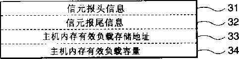
图2显示了传统ATM通信设备中发送参数存储部分7(见图1)的格式。FIG. 2 shows the format of the transmission parameter storage section 7 (see FIG. 1) in a conventional ATM communication device.
如图2所示,就一个VC而言,发送参数存储部分7中保存有信元报头信息31,信元报尾信息32,有效负载在主机内存3中的存储地址33(主机内存有效负载存储地址说明了有效负载存储区在主机内存3中的起始地址),以及主机内存有效负载容量34(它说明了在从有效负载存储地址33开始的连续区域中保存的有效负载的字节数)。尽管在图2中仅显示了一个VC的存储信元(存储部分),但类似的存储部分存在于所有其它VC的发送参数存储部分7之中。As shown in Figure 2, with respect to a VC,
如图1所示,传统ATM通信设备1包括以下信号线:VC序号信号线19,发送参数信号线20,DMA开始请求信号线21,有效负载数据信号线25,报头/报尾数据信号线26,以及信元数据信号线27。以下将参考图1对各信号线进行详细说明。As shown in Figure 1, traditional
发送调度部分8利用VC序号信号线19将VC序号通知给信元形成/发送控制部分6,以确定下一个将要发送的VC。发送参数信号线20用于在信元形成/发送控制部分6和发送参数存储部分7之间交换发送参数。The
信元形成/发送控制部分6利用DMA开始请求信号线21将DMA的读入地址和DMA读入数据的长度通知给主机总线接口部分5,以开始DMA传送。主机总线接口部分5利用有效负载数据信号线25向发送信元形成部分9发送有效负载数据DMA一读。The cell formation/
报头/报尾数据信号线26用于向发送信元形成部分9发送信元报头信息31和信元报尾信息32(见图2),报头信息31和报尾信息32是由信元形成/发送控制部分6通过发送参数信号线20从发送参数存储部分7中读出的。信元数据信号线27用于将由发送信元形成部分9形成的发送信元保存在发送数据FIFO 10中。Header/tail data signal line 26 is used to send
图3的流程图显示了传统ATM通信设备的操作流程。以下将参考图3以及图1和图2对传统ATM通信设备的操作流程进行说明。The flow chart of Fig. 3 shows the operation flow of the conventional ATM communication equipment. The operation flow of the conventional ATM communication equipment will be described below with reference to FIG. 3 and FIG. 1 and FIG. 2 .
在传统ATM通信设备中,当要对下一个信元进行发送时,发送调度部分8将通过VC序号信号线19把信元的VC序号通知给信元形成/发送控制部分6(步骤S1“VC序号通知”)。In the traditional ATM communication equipment, when the next cell will be sent, the sending
根据接收到的VC信元序号通知,信元形成/发送控制部分6将通过DMA开始请求信号线21向主机总线接口部分5通知主机内存的有效负载存储地址33(它作为DMA读入地址而保存在发送参数存储部分7之中)和48个字节(该数值代表了上一个信元的主机内存有效负载容量34)长度的DMA读入数据。然后,信元形成/发送控制部分6给指导主机总线接口部分5提供一个指令以DMA-读入与主机内存3中的一个信元相对应的发送有效负载。Notify according to the VC cell sequence number that receives, cell forms/sends
根据所接收的上述指令,主机总线接口部分5将在当与一个或多个信元相对应的发送有效负载保存在主机内存3中的连续地址区域时,用一个总线周期来DMA-读入1个信元的数据,并且DMA读入可通过主机总线4的结构而连续完成。According to the above instruction received, the host
如果发送有效负载分布在主机内存3中的不同地址区域,或DMA读入不能通过主机总线4的结构而连续完成,则一个信元数据的DMA读入将在多个总线周期中完成。由DMA读入的发送有效负载被送往发送信元形成部分9。在发送信元形成部分9中,有效负载、信元报头信息31及信元报尾信息32被封装进一个信元。而此信元被保存在发送数据FIFO 10之中。If the sending payload is distributed in different address areas in the
发送调度部分8以信元为单位对发送VC进行选择,而且没有必要为两个信元连续地选择相同的VC。由于这个原因,使得发送有效负载的DMA读入、发送信元的形成、以及在发送数据FIFO 10中的数据写都以信元为单位而进行(步骤S2“传送一个信元”)。The
进行这种操作的原因如下。假设发送调度部分8选中了一个给定VC以作为发送VC。在这种情况下,如果与该VC相对应的两个或多个信元的有效负载数据被保存在发送数据FIFO 10中,则当发送调度部分8选中另一个VC以作为下一个发送VC时,发送顺序将被打乱。The reason for this operation is as follows. Assume that the
保存在发送数据FIFO 10之中的发送信元被通过物理层设备接口11送往物理层设备(步骤S3“发送一个信元”)。The sending cell stored in the sending data FIFO 10 is sent to the physical layer device through the physical layer device interface 11 (step S3 "send a cell").
在上述ATM通信设备(以下称现有技术)中存在以下问题(第一和第二问题)。There are the following problems (first and second problems) in the above-mentioned ATM communication device (hereinafter referred to as prior art).
第一个问题是:主机总线(见图1中的参考序号4)的传送效率很低。The first problem is that the transfer efficiency of the host bus (see
其原因在于,在现有技术中,对发送数据以信元为单位的DMA读入将产生一个额外开销,该额外开销与用于各DMA读入所进行的总线访问及类似过程的判断有关。假设该ATM通信设备通过一个PCI总线接口从主机内存中主读入有效负载数据,在这种情况下,至少需要两个时钟周期的时间以使该ATM通信设备获得总线访问(即,将REQ#信号设定为低电平之后,再通过获得一GNT#信号以将一FRAME#信号设定为低电平,这期间所需的时间)。另外,由于在该ATM通信设备输出一个地址后,还至少需要两个时钟周期的时间以从主机内存中接收第一个字的数据,所以用于各DMA读入的总额外开销至少为2+2=4个时钟周期。The reason for this is that, in the prior art, the DMA read-in of the transmitted data in units of cells generates an overhead which is related to the judgment of the bus access and the like for each DMA read-in. Supposing that this ATM communication equipment reads in payload data from the host computer memory main frame by a PCI bus interface, in this case, need the time of two clock cycles at least to make this ATM communication equipment obtain bus access (that is, set REQ# After the signal is set to a low level, a GNT# signal is obtained to set a FRAME# signal to a low level, the time required during this period). In addition, since the ATM communication device needs at least two clock cycles to receive the first word of data from the host memory after outputting an address, the total overhead for each DMA read-in is at least 2+ 2 = 4 clock cycles.
实际情况中,总线访问时间所需的时间还要更长。另外,在ATM通信设备输出一个地址的时刻与第一个字的数据被从主机内存中接收到的时刻之间的时间间隔内,一般还有一个等待时间。在这种情况下,随着位于ATM通信设备与主机内存之间的PCI总线的越发拥塞,总线访问时间越长,或者从主机内存中接收有效负载数据的延迟越多,第一个问题将更加明显。In practice, the bus access time takes even longer. In addition, there is generally a wait time between the time when the ATM communication device outputs an address and the time when the first word of data is received from the host memory. In this case, as the PCI bus between the ATM communication device and the host memory becomes more congested, the bus access time is longer, or the delay in receiving the payload data from the host memory is greater, the first problem will be more serious. obvious.
第二个问题是:在信元发送确定和实际发送之间有较长的延迟。这是因为,DMA读入必须总在信元发送确定(发送VC确定)之后才能完成,因此由DMA读入所需额外开销所造成的延迟将不可避免地发生在各个信元之中。The second problem is that there is a long delay between the determination of cell transmission and the actual transmission. This is because DMA read-in must always be completed after the cell transmission is confirmed (the sending VC is confirmed), so the delay caused by the overhead required for DMA read-in will inevitably occur in each cell.
随着位于ATM通信设备与主机内存之间的PCI总线的越发拥塞,总线访问时间越长,或者从主机内存中接收有效负载数据的延迟越多,第二个问题也将更为明显。The second problem will become more pronounced as the PCI bus between the ATM communication device and host memory becomes more congested, the bus access times become longer, or the delay in receiving payload data from host memory increases.
本发明是考虑现有技术中的上述情况而形成的,其目的是提供这样一种ATM通信设备,它可通过提高主机的总线传送效率来减少信元发送确定时刻与信元实际发送时刻之间的延迟。The present invention is formed in consideration of the above-mentioned situation in the prior art, and its purpose is to provide such an ATM communication device, which can reduce the time difference between the cell transmission confirmation time and the cell actual transmission time by improving the bus transmission efficiency of the host computer. Delay.
一种根据本发明的ATM通信设备,它能够在一个总线周期内将与多个信元相对应的发送数据DMA-读入一个内部缓冲器,并能通过从该缓冲器中读出发送数据来发送ATM信元。更具体地说,这种ATM通信设备联合使用了发送数据临时存储部分(它能够以VC为单位,对与多个信元相对应的发送数据进行存储/管理)和一能够在一个总线周期内将与多个信元相对应的发送数据DMA读入临时存储部分的装置。A kind of ATM communication equipment according to the present invention, it can DMA-read the sending data corresponding to a plurality of letter elements into an internal buffer in one bus cycle, and can read the sending data by reading out the sending data from this buffer Send ATM cells. More specifically, this ATM communication equipment has jointly used a transmission data temporary storage part (which can store/manage transmission data corresponding to a plurality of cells in units of VCs) and a transmission data which can be stored in one bus cycle. Means for DMA-reading transmission data corresponding to a plurality of cells into a temporary storage section.
为达到上述目的,就主要方面而言,本发明提供的一种ATM通信设备包括:In order to achieve the above object, in terms of main aspects, a kind of ATM communication equipment provided by the present invention comprises:
发送调度装置,它用于确定将要发送的虚拟信道;sending scheduling means, which is used to determine the virtual channel to be sent;
信元报头存储装置,它用于保存发送信元的报头信息;A cell header storage device, which is used to store the header information of the sent cell;
信元报尾存储装置,它用于保存发送信元的报尾信息;A cell trailer storage device, which is used to store the trailer information of the sent cell;
有效负载读入装置,它用于从主机内存中读出有效负载数据;以及payload read-in means for reading payload data from host memory; and
发送信元形成装置,它用于将从主机内存中读出的有效负载数据、信元报头信息及信元报尾信息组成一个发送信元。The sending cell forming device is used for forming a sending cell from the payload data read from the host memory, the cell header information and the cell trailer information.
此ATM通信设备能够为一给定虚拟信道从主机内存中读出有效负载数据,在发送调度装置确定该给定虚拟信道发送时,将有效负载数据、信元报头信息及信元报尾信息组成一个发送信元,并将该信元发送到物理层设备上。The ATM communication equipment can read the payload data from the host memory for a given virtual channel, and when the sending scheduling device determines that the given virtual channel is sent, the payload data, the cell header information and the cell trailer information are composed One transmits the cell and sends the cell to the physical layer device.
这种ATM通信设备的特征在于它还包括:This ATM communication equipment is characterized in that it also includes:
发送有效负载存储装置,它用于以虚拟信道为单位来保存与多个信元相对应的有效负载;sending payload storage means for storing payloads corresponding to a plurality of cells in units of virtual channels;
有效负载存储位置存储装置,它用于保存在发送有效负载存储装置中所存储的各有效负载的位置信息;和payload storage location storage means for storing the location information of each payload stored in the transmission payload storage means; and
被存储有效负载计数存储装置,它用于保存说明有效负载当前所在存储区域的信息,而该区域则由与指定信元序号相对应的有效负载存储位置来表示。Stored payload count storage means for holding information describing the storage area where the payload is currently located, and the area is represented by the payload storage location corresponding to the specified cell number.
当发送调度装置确定一个发送虚拟信道,并且如果在发送有效负载存储装置中没有该虚拟信道的有效负载时,与多个信元相对应的有效负载数据将被从主机内存中读出。然后,对应于第一信元的有效负载、信元报头及信元报尾将被组成一个发送信元。该信元被发送到物理层设备上。而与第二及其它顺序信元相对应的有效负载则被临时保存在发送有效负载存储装置中。When the transmission scheduling means determines a transmission virtual channel, and if there is no payload of the virtual channel in the transmission payload storage means, payload data corresponding to a plurality of cells will be read from the host memory. Then, the payload, cell header and cell trailer corresponding to the first cell will be composed into a transmit cell. The cell is sent to the physical layer device. The payloads corresponding to the second and other sequential cells are temporarily stored in the transmit payload storage means.
当发送调度装置将虚拟信道确定为下一个发送虚拟信道,并且如果在发送有效负载存储装置中存有有效负载时,该有效负载将被直接从发送有效负载存储装置中读出。然后,该有效负载、对应的信元报头及信元报尾将被组成一个发送信元。该信元被发送到物理层设备上。When the transmission scheduling means determines the virtual channel as the next transmission virtual channel, and if there is a payload stored in the transmission payload storage means, the payload will be directly read from the transmission payload storage means. Then, the payload, corresponding cell header and cell trailer will be composed into a transmit cell. The cell is sent to the physical layer device.
根据本发明的另一个方面,在此ATM通信设备中,当发送调度装置确定一虚拟信道时,即使用于该发送虚拟信道的有效负载序数(保存在发送有效负载存储装置中)不是0但未超过一预定阈值,有效负载数据也可以被从主机内存中重新读出,并被加入/存储到发送有效负载存储装置中。According to another aspect of the present invention, in this ATM communication equipment, when sending scheduling means to determine a virtual channel, even if the payload sequence number (saved in sending payload storage means) for this sending virtual channel is not 0 but not Beyond a predetermined threshold, payload data may also be read from host memory and added/stored to the send payload storage device.
在根据本发明所述的ATM通信设备中,用于待发送VC的对应于多个信元的发送数据可以在一个总线周期内被DMA读入发送数据临时存储装置。对于第二个及其后的信元来说,发送数据可从内部缓冲器中直接读出而不需使用主机总线。In the ATM communication device according to the present invention, the sending data corresponding to a plurality of cells for the VC to be sent can be read into the sending data temporary storage device by DMA within one bus cycle. For the second and subsequent cells, transmit data can be read directly from the internal buffer without using the host bus.
因此,本发明具有以下效果。Therefore, the present invention has the following effects.
第一个效果是提高了主机总线的利用率,其原因如下。The first effect is increased host bus utilization for the following reasons.
根据本发明所述,由于该ATM通信设备利用了能够以VC为单位保存与多个信元相对应的有效负载数据的存储装置,使得与多个信元相对应的有效负载数据能够在一个总线周期内被读入ATM通信设备。此举减小了伴随着数据传送的额外开销。According to the present invention, since the ATM communication equipment utilizes a storage device capable of storing payload data corresponding to multiple cells in units of VCs, the payload data corresponding to multiple cells can be stored on one bus is read into the ATM communication device during the period. This reduces the overhead that accompanies data transfer.
假设该ATM通信设备通过PCI总线接口从主机内存中主读入有效负载数据,在这种情况下,至少需要两个时钟周期的时间以使该ATM通信设备获得总线访问(即,将REQ#设定为低电平以获得GNT#的时刻与FRAME#信号以低电平输出的时刻之间的时间间隔)。另外,在该ATM通信设备输出一个地址后,还至少需要两个时钟周期的时间以从主机内存中接收第一个字的数据,也就是说,每个DMA读入的总额外开销至少为2+2=4个时钟周周期。Supposing that this ATM communication equipment reads in the effective load data from main frame internal memory by PCI bus interface, in this case, need the time of two clock cycles at least so that this ATM communication equipment obtains bus access (that is, REQ# is set to Set as low level to obtain the time interval between the moment of GNT# and the moment of FRAME# signal output at low level). In addition, after the ATM communication device outputs an address, it takes at least two clock cycles to receive the first word of data from the host memory, that is, the total overhead for each DMA read is at least 2 +2 = 4 clock cycles.
假设对应于一个信元的有效负载数据被输出到总线上的总时间为12个时钟周期。在现有技术中,以信元为单位读出对应于5个信元的有效负载数据所需的时间至少为(2+2+12)×5=80个时钟周期。而在本发明中,在一个总线周期内读出对应于5个信元的有效负载数据所需的时间只有2+2+(12×5)=64个时钟周期。Assume that the total time for the payload data corresponding to one cell to be output on the bus is 12 clock cycles. In the prior art, it takes at least (2+2+12)×5=80 clock cycles to read the payload data corresponding to 5 cells in units of cells. However, in the present invention, the time required to read the payload data corresponding to 5 cells in one bus cycle is only 2+2+(12*5)=64 clock cycles.
实际情况中,总线访问时间所需的时间要超过上述时间。另外,在ATM通信设备输出一个地址的时刻与第一个字的数据被从主机内存中接收到的时刻之间的时间间隔内,一般还有一个等待时间。在这种情况下,随着位于ATM通信设备与主机内存之间的PCI总线的越发拥塞,总线访问时间越长,或者从主机内存中接收有效负载数据的延迟越多,本发明对ATM通信设备中主机总线利用率的提高也相应更大。In reality, the bus access time takes longer than the above time. In addition, there is generally a wait time between the time when the ATM communication device outputs an address and the time when the first word of data is received from the host memory. In this case, as the PCI bus between the ATM communication device and the host memory becomes more and more congested, the bus access time is longer, or the delay of receiving payload data from the host memory is more, the present invention has a significant impact on the ATM communication device. The increase in host bus utilization is correspondingly greater.
本发明的第二个效果是使得信元发送确定时刻与实际发送时刻之间的延迟较小,其原因如下。The second effect of the present invention is to make the delay between the cell transmission determination time and the actual transmission time small for the following reason.
根据本发明,该ATM通信设备利用了能够以VC为单位保存与多个信元相对应的有效负载数据的存储装置,而与第二个及其后信元相对应的有效负载数据被临时保存在这个存储装置中。在信元发送过程中,有效负载被从内部存储区读出而无需使用总线,因此避免了由于使用总线而造成的读延迟。According to the present invention, the ATM communication apparatus utilizes storage means capable of storing payload data corresponding to a plurality of cells in units of VCs, while payload data corresponding to the second and subsequent cells are temporarily stored in this storage device. During cell transmission, the payload is read from the internal storage area without using the bus, thus avoiding the read delay caused by using the bus.
例如,考虑一下,当与一个信元相对应的有效负载数据被通过PCI总线接口主读入时所造成的读入延迟。至少需要两个时钟周期的时间以使ATM通信设备在将REQ#设定为低电平以获得GNT#之后,以低电平输出FRAME#信号。另外,在该ATM通信设备输出一个地址后,还至少需要两个时钟周期的时间以从主机内存中接收第一个字的数据,因而至少发生了4个时钟周期的延迟。For example, consider the read-in delay caused when the payload data corresponding to one cell is read in by the master through the PCI bus interface. It takes at least two clock cycles for the ATM communication device to output the FRAME# signal at a low level after setting REQ# to a low level to obtain GNT#. In addition, after the ATM communication device outputs an address, it takes at least two clock cycles to receive the first word of data from the host memory, so at least four clock cycles are delayed.
与之相比,在本发明中,在从ATM通信设备中的有效负载数据存储装置读入1个信元的数据的过程中没有不确定因素,即,总线访问时间。因此,即使此设备与类似的PCI总线接口相连接,也只需考虑两个时钟周期的已知值。In contrast, in the present invention, there is no uncertain factor, ie, bus access time, in the process of reading in data of 1 cell from the payload data storage means in the ATM communication device. Therefore, even if this device is interfaced with a similar PCI bus, only the known value of two clock cycles needs to be considered.
实际情况中,总线访问时间所需的时间要超过上述时间。另外,在ATM通信设备输出一个地址的时刻与第一个字的数据被从主机内存中接收到的时刻之间的时间间隔内,一般还有一个等待时间。在这种情况下,随着位于ATM通信设备与主机内存之间的PCI总线的越发拥塞,总线访问时间越长,或者从主机内存中接收有效负载数据的延迟越多,本发明所述的ATM通信设备可获得明显的延迟减少效果。In reality, the bus access time takes longer than the above time. In addition, there is generally a wait time between the time when the ATM communication device outputs an address and the time when the first word of data is received from the host memory. In this case, as the PCI bus between the ATM communication device and the host memory becomes more congested, the bus access time is longer, or the delay in receiving payload data from the host memory is more, the ATM of the present invention A significant delay reduction effect can be obtained for the communication device.
通过以下详细说明并参考附图(其中通过图例显示了体现本发明原则的实施例),本发明的其它目的、特征和优点对熟练的技术人员来说将变得更为清楚。Other objects, features and advantages of the present invention will become more apparent to those skilled in the art from the following detailed description, taken with reference to the accompanying drawings, in which are shown by way of illustrations embodiments embodying the principles of the invention.
图1为传统ATM通信设备的结构示意框图。Fig. 1 is a schematic block diagram of the structure of a traditional ATM communication device.
图2为图1所示现有技术中发送参数存储部分的格式图。FIG. 2 is a format diagram of the sending parameter storage part in the prior art shown in FIG. 1 .
图3为图1所示现有技术的操作流程图。FIG. 3 is an operation flowchart of the prior art shown in FIG. 1 .
图4为根据本发明第一个实施例所述ATM通信设备的结构示意图。Fig. 4 is a schematic structural diagram of the ATM communication device according to the first embodiment of the present invention.
图5为本发明第一个实施例中发送参数存储部分的格式图。Fig. 5 is a format diagram of the transmission parameter storage part in the first embodiment of the present invention.
图6为本发明第一个实施例的操作流程图。Fig. 6 is an operation flowchart of the first embodiment of the present invention.
图7为根据本发明第二个实施例所述ATM通信设备的结构示意图。Fig. 7 is a schematic structural diagram of the ATM communication device according to the second embodiment of the present invention.
图8为本发明第二个实施例中的随机存取存储器经初始化后的内容结构图。FIG. 8 is a structure diagram of the initialized contents of the random access memory in the second embodiment of the present invention.
图9为本发明第二个实施例中的随机访问存储器在其部分随机存储器被分配给发送VC时的内容结构图。FIG. 9 is a structural diagram of the random access memory in the second embodiment of the present invention when part of the random access memory is allocated to the sending VC.
图10为本发明第二个实施例中发送参数存储部分的格式图。Fig. 10 is a format diagram of the transmission parameter storage part in the second embodiment of the present invention.
图11为本发明第三个实施例中发送参数存储部分的格式图。Fig. 11 is a format diagram of the transmission parameter storage part in the third embodiment of the present invention.
图12为本发明第三个实施例的操作流程图。Fig. 12 is an operation flowchart of the third embodiment of the present invention.
以下将参考附图对本发明的多个实施例进行详细说明。Various embodiments of the present invention will be described in detail below with reference to the accompanying drawings.
图4为根据本发明第一个实施例所述ATM通信设备的结构示意图。Fig. 4 is a schematic structural diagram of the ATM communication device according to the first embodiment of the present invention.
如图4所示,与参考图1对传统ATM通信设备(现有技术)的说明相类似,一种根据本发明第一个实施例所述的ATM通信设备1具有一个ATM信元形成/发送部分,它由发送调度部分8、信元形成/发送控制部分6、发送参数存储部分7、发送信元形成部分9以及发送数据FIFO 10构成。该ATM通信设备1的接收/分隔部分由接收/信元分隔控制部分12、接收数据FIFO 13、用于向/从主机系统发送/接收数据的主机总线接口部分5、以及用于向/从物理层设备发送/接收ATM信元的物理层设备接口部分11构成。As shown in Figure 4, similar to the description of conventional ATM communication equipment (prior art) with reference to Figure 1, a kind of
根据本发明第一个实施例所述的ATM通信设备1还含有一个位于发送数据FIFO 10和主机总线接口部分5之间、能为各VC保存有效负载的发送有效负载临时存储部分14。According to the described
如图4所示,发送有效负载临时存储部分14含有多个有效负载FIFO 17。各有效负载FIFO 17被分别分配给不同的VC。发送有效负载临时存储部分14还含有一个FIFO控制部分18,它用于将FIFO分配给VC并管理已分配给VC的空闲有效负载FIFO 17。该部分14还含有用于控制有效负载数据流的第一和第二选择器15和16。As shown in FIG. 4, the transmit payload
图4中的ATM通信设备1通过主机内存4与主机CPU2和主机内存3相连接。The
图5为本发明第一个实施例中发送参数存储部分7的格式图。如图5所示,就一个VC而言,发送参数存储部分7中保存有信元报头信息31,信元报尾信息32,主机内存有效负载存储地址33以及主机内存有效负载容量34。它与现有技术中的格式相同。FIG. 5 is a format diagram of the transmission
如图5所示,除上述各项信息之外,本发明第一个实施例中的发送参数存储部分7还保存:As shown in Figure 5, in addition to the above-mentioned items of information, the sending
多信元连续传送允许/禁止信息35,它说明主机CPU2是否一次完成将与多个信元相对应的发送有效负载从主机内存3传送到VC中;Multi-cell continuous transmission permission/
有效负载FIFO序号36,它说明是否有代表有效负载FIFO 17的指定序号被分配给VC;Payload FIFO number 36, which indicates whether a specified number representing
临时存储部分剩余有效负载计数37,它说明与有效负载FIFO 17(由有效负载FIFO号36表示)中当前剩余有效负载相对应的信元序号。A partial remaining
尽管在图5中仅显示了一个VC的存储信元(存储部分),但类似的存储部分在所有其它VC的发送参数存储部分7之中也有。Although only a storage cell (storage section) of one VC is shown in FIG. 5, similar storage sections are present in the transmission
与现有技术相同,图4所示的ATM通信设备1包括以下信号线:VC序号信号线19,发送参数信号线20,DMA开始请求信号线21,有效负载数据信号线25,报头/报尾数据信号线26,以及信元数据信号线27。该ATM通信设备1还包括一个FIFO控制信息信号线22,一选择信息信号线23以及一选择信息信号线24。Same as prior art, the
信元形成/发送控制部分6利用FIFO控制信息信号线22来请求FIFO控制部分18给VC分配一个有效负载FIFO 17,而且FIFO控制部分18还利用FIFO控制信息信号线22将分配给VC的有效负载FIFO 17的序号通知给信元形成/发送控制部分6。The cell formation/
信元形成/发送控制部分6利用选择信息信号线23将用于把有效负载输出目标切换为另一个的命令通知给第一选择器15。信元形成/发送控制部分6利用选择信息信号线24将用于把有效负载输出目标切换为另一个的命令通知给第二选择器16。The cell formation/
图6为本发明第一个实施例的操作流程图。以下将参考图6和图4及图5对本发明第一个实施例的操作流程进行信息说明。Fig. 6 is an operation flowchart of the first embodiment of the present invention. The operation flow of the first embodiment of the present invention will be described below with reference to FIG. 6 , FIG. 4 and FIG. 5 .
在根据本发明第一个实施例所述的ATM通信设备1中,当要对下一个信元进行发送时,发送调度部分8将通过VC序号信号线19把信元的VC序号通知给信元形成/发送控制部分6(步骤S1“VC序号通知”)。In the
根据接收到的VC信元序号通知,信元形成/发送控制部分6将搜寻保存于发送参数存储部分7之中的多信元连续传送允许/禁止信息35,以检查是否可以将与多个信元相对应的有效负载连续传送到VC(步骤S11“连续传送VC?”)。According to the received VC cell sequence number notification, the cell formation/
多信元连续传送允许/禁止信息35由主机CPU2确定并被事先设置好。如果主机CPU2不想向VC连续传送有效负载,则流程将转向步骤S2,从而只用DMA-读入对应于一个信元的有效负载。The multi-cell continuous transfer enable/disable
如果主机CPU2想要向VC连续传送多个有效负载,信元形成/发送控制部分6将搜寻保存于发送参数存储部分7之中的临时存储部分剩余有效负载计数37,以检查用于VC的发送有效负载是否已经被存入发送有效负载临时存储部分14(步骤S12“存储了数据?”)。If the
如果其中存有有效负载,则流程将转向步骤S17,以从发送有效负载临时存储部分14中读出并发送对应于一个信元的有效负载。If there is a payload stored therein, the flow goes to step S17 to read and transmit the payload corresponding to one cell from the transmission payload
如果其中未保存有效负载,则信元形成/发送控制部分6将搜寻保存于发送参数存储部分7之中的主机内存有效负载容量34,以检查与VC的多个信元相对应的有效负载是否可以被一次DMA-读入(各信元序号可被连续DMA-读入)(步骤S13“连续数据?”)。如果确定在主机内存3的连续地址区域中没有保存与两个信元(96字节)或更多信元相对应的有效负载,流程将转向步骤S2,从而只用DMA-读入对应于一个信元的有效负载。If no payload is stored therein, the cell formation/
如果其中保存有与两个或更多信元相对应的有效负载,则信元形成/发送控制部分6将通过FIFO控制信息信号线22向FIFO控制部分18输出一个存储区域获得请求,以通过将发送有效负载临时存储部分14中的一个有效负载FIFO 17分配给该VC来获得一个存储区域。根据接收到的请求,FIFO控制部分18通过FIFO控制信息信号线22将空闲有效负载FIFO 17序号通知给信元形成/发送控制部分6。如果没有空闲有效负载FIFO 17,则FIFO控制部分18将把序号0通知给信元形成/发送控制部分6。If the effective load corresponding to two or more cells is stored therein, the cell formation/
这个被通知的有效负载FIFO序号将作为有效负载FIFO序号36被保存在发送调度部分8中,以用于从发送有效负载临时存储部分14中读出有效负载并发送它们(步骤S14“输出存储区域请求”)。This notified payload FIFO sequence number will be saved in the
在步骤S14中,当将有效负载FIFO 17分配给VC的工作完成时,信元形成/发送控制部分6会检查保存在发送参数存储部分7之中的有效负载FIFO序号36。如果此有效负载FIFO序号36不是0,则信元形成/发送控制部分6将确定与该VC相对应的发送有效负载可以被保存在发送有效负载临时存储部分14中。然后流程转向步骤S16,以进行与多个信元相对应的有效负载的连续DMA传送。如果此有效负载FIFO序号36为0,并且没有空闲有效负载FIFO 17分配给VC,则信元形成/发送控制部分6将确定:该发送有效负载不能被保存在发送有效负载临时存储部分14中。然后流程转向步骤S2,从而只用DMA-读入对应于一个信元的有效负载(步骤S15“是否保存数据?”)。In step S14, when the assignment of the
在步骤S15中,如果信元形成/发送控制部分6确定要执行与多个信元相对应的有效负载的连续DMA传送。则部分6将通过DMA开始请求信号线21向主机总线接口部分5通知DMA读入地址和DMA读入数据长度,并输出一个指令以从主机内存3中用DMA-读入发送有效负载。此时,信元形成/发送控制部分6将把保存于发送参数存储部分7之中的主机内存有效负载存储地址33作为DMA读入地址而通知给主机总线接口部分5。In step S15, if the cell formation/
在通知DMA读入数据长度的过程中,信元形成/发送控制部分6将对可被连续DMA读入信元(由步骤S12确定)的序号减一的信元序号和可以被保存在有效负载FIFO(有效负载FIFO的容量)之中的信元的序号进行比较,并将上述两信元序号中较小的一个加1,以作为可以被DMA-读入的有效负载的信元序号通知给主机总线接口部分5。In the process of notifying the DMA to read in the data length, the cell formation/
信元形成/发送控制部分6将通过选择信息信号线23和选择信息信号线24,把用于说明当前将要传送的与多个信元相对应的数据的信息以及作为命令的有效负载FIFO序号36通知给第一和第二选择器15及16。第一和第二选择器15及16利用命令解码器将这些通知作为命令来处理。The cell formation/
第一和第二选择器15及16通过选择一条避开有效负载FIFO 17的路径,直接将第一DMA-读入发送有效负载中1个信元的有效负载发送到发送信元形成部分9。The first and
对剩余的有效负载来说,第一选择器15将其输出切换到一条通往有效负载FIFO 17(由有效负载FIFO序号36指定)的路径上,以将该有效负载保存在发送有效负载临时存储部分14中的有效负载FIFO 17内(步骤S16“传送有效负载至存储区域”)。For the remaining payload, the
在步骤S2中,与现有技术相同,与一个信元相对应的有效负载被DMA-读入。在这种情况下,信元形成/发送控制部分6通过选择信息信号线23和选择信息信号线24向发送有效负载临时存储部分14中的第一和第二选择器15及16发出跳过有效负载FIFO 17的命令,并将有效负载直接送往发送信元形成部分9。In step S2, the payload corresponding to one cell is DMA-read in as in the prior art. In this case, the cell formation/
如果信元形成/发送控制部分6在步骤S12中确定:从发送有效负载临时存储部分14中读出并将要发送的是与一个信元相对应的有效负载,则信元形成/发送控制部分6将发出命令以把第二选择器16的输入切换到由有效负载FIFO序号36指定的有效负载FIFO 17上,由此将有效负载从发送有效负载临时存储部分14发送到发送信元形成部分9。If the cell formation/
在此之后,信元形成/发送控制部分6将对保存在发送参数存储部分7之中的临时存储部分剩余有效负载计数37进行减一操作(步骤S17“从存储区域中读出有效负载”)。After that, the cell formation/
发送有效负载被送往发送信元形成部分9,与信元报头信息31和信元报尾信息32一起组成一个发送信元。该信元被保存在发送数据FIFO 10中,然后通过物理层设备接口11被送往物理层设备(步骤S3“发送一个信元”)。The transmission payload is sent to the transmission
以下将对本发明第二个实施例进行详细说明。The second embodiment of the present invention will be described in detail below.
图7为根据本发明第二个实施例所述ATM通信设备的结构框图。Fig. 7 is a structural block diagram of the ATM communication device according to the second embodiment of the present invention.
在图4所示的第一个实施例中,发送有效负载临时存储部分14中的有效负载存储区域由多个有效负载FIFO 17构成。与之相反,在第二个实施例中使用了一个RAM41(随机存取存储器)来作为有效负载存储区域。该RAM 41和用于管理RAM 41的缓冲器控制部分42一起构成了一个发送有效负载临时存储部分14。第二个实施例中含有一个缓冲器控制信息信号线43,它取代了FIFO控制信息信号线22。由于剩余的其它结构与第一个实施例中的结构完全相同,故此略去说明。In the first embodiment shown in FIG. In contrast, a RAM 41 (Random Access Memory) is used as a payload storage area in the second embodiment. The
图8为本发明第二个实施例中的随机存取存储器经初始化后的内容结构图。FIG. 8 is a structure diagram of the initialized contents of the random access memory in the second embodiment of the present invention.
如图8所示,RAM41的整个区域被划分为多个具有相同结构的空闲有效负载存储块,即,空闲有效负载存储块(1)51a,空闲有效负载存储块(2)51b,空闲有效负载存储块(3)51c,空闲有效负载存储块(4)51d,空闲有效负载存储块(5)51e及空闲有效负载存储块(6)51f。注意,以下将把具有与空闲有效负载存储块(1)51a相同格式的区域都称为有效负载存储块。As shown in FIG. 8, the entire area of
当具有相同长度的各有效负载存储块被分配给VC时,与一个信元相对应的发送有效负载将被保存在各有效负载存储块中。用于相互逻辑链接多个有效负载存储块的前向链路地址被保存在全部有效负载存储块的末端。这些前向链路地址将作为所谓的链接指针来使用。When payload storage blocks having the same length are allocated to VCs, transmission payloads corresponding to one cell will be stored in each payload storage block. A forward link address for logically linking a plurality of payload storage blocks to each other is stored at the end of all payload storage blocks. These forward link addresses will be used as so-called link pointers.
前向链路地址(1)52a,前向链路地址(2)52b,前向链路地址(3)52c,前向链路地址(4)52d,前向链路地址(5)52e及前向链路地址(6)52f分别保存在空闲有效负载存储块(1)51a,空闲有效负载存储块(2)51b,空闲有效负载存储块(3)51c,空闲有效负载存储块(4)51d,空闲有效负载存储块(5)51e及空闲有效负载存储块(6)51f之中。forward link address (1) 52a, forward link address (2) 52b, forward link address (3) 52c, forward link address (4) 52d, forward link address (5) 52e and The forward link address (6) 52f is respectively stored in the free payload storage block (1) 51a, the free payload storage block (2) 51b, the free payload storage block (3) 51c, and the free payload storage block (4) 51d, among the free payload storage block (5) 51e and the free payload storage block (6) 51f.
前向链路地址(1)52a指定了空闲有效负载存储块(2)51b的起始地址;前向链路地址(2)52b指定了空闲有效负载存储块(3)51c的起始地址;前向链路地址(3)52c指定了空闲有效负载存储块(4)51d的起始地址;前向链路地址(4)52d指定了空闲有效负载存储块(5)51e的起始地址;前向链路地址(6)52f指定了空闲有效负载存储块(6)51f的起始地址,因此将空闲有效负载存储块(1)51a到空闲有效负载存储块(6)51f逻辑链接起来。其结果是形成了一个空闲有效负载存储块链53a。The forward link address (1) 52a specifies the starting address of the free payload storage block (2) 51b; the forward link address (2) 52b specifies the starting address of the free payload storage block (3) 51c; The forward link address (3) 52c specifies the starting address of the free payload storage block (4) 51d; the forward link address (4) 52d specifies the starting address of the free payload storage block (5) 51e; Forward link address (6) 52f specifies the starting address of free payload storage block (6) 51f, thus logically linking free payload storage block (1) 51a to free payload storage block (6) 51f. The result is a free payload
作为空闲有效负载存储块链53a起始有效负载存储块的空闲有效负载存储块(1)51a,它的起始地址将作为空闲有效负载存储块链起始地址54而被保存在缓冲器控制部分42中,以用于建立一个新的链接。The start address of the free payload storage block (1) 51a which is the starting payload storage block of the free payload
与空闲有效负载存储块链53a的末端相链接的空闲有效负载存储块(6)51f,它的起始地址将作为空闲有效负载存储块链末端地址59而被保存在缓冲器控制部分42中,以用于建立一个新的链接。The start address of the free payload storage block (6) 51f linked to the end of the free payload
初始化之后,RAM 41中的有效负载存储块未被分配给任何VC。After initialization, the payload storage block in
在发送一个有效负载的过程中,根据将要建立的一个新链接,有效负载存储块被从空闲有效负载存储块链53a中提取出来,并且这个提取出来的有效负载存储块通过利用前向链路地址被链接以形成一个更大的有效负载存储区域(有效负载存储块链)。该区域被分配给VC以用作有效负载的临时存储区域。In the process of sending a payload, according to a new link to be established, the payload storage block is extracted from the free payload
图9为本发明第二个实施例中的随机随取存储器在其部分随机存储器被分配给发送VC时的内容结构图。FIG. 9 is a content structure diagram of the random random access memory in the second embodiment of the present invention when part of the random random memory is allocated to the sending VC.
以下将参考图9对RAM 41在空闲有效负载存储块链53a的四个有效负载存储块被分配给VC 1情况下的结构进行详细说明。The structure of the
参考图9,空闲有效负载存储块链53a的四个空闲有效负载存储块(从第一块到第四块)分别为空闲有效负载存储块(1)51a,空闲有效负载存储块(2)51b,空闲有效负载存储块(3)51c及空闲有效负载存储块(4)51d。它们被从空闲有效负载存储块链53a的起始处分开,并分别被分配为VC 1有效负载存储块(1)55a,VC 1有效负载存储块(2)55b,VC 1有效负载存储块(3)55c及VC 1有效负载存储块(4)55d。这些块将用作VC 1的发送有效负载存储区域。Referring to Fig. 9, four free payload storage blocks (from the first block to the fourth block) of the idle payload
在VC 1有效负载存储块(1)55a,VC 1有效负载存储块(2)55b,VC 1有效负载存储块(3)55c及VC 1有效负载存储块(4)55d中分别保存有前向链路地址(1)56a,前向链路地址(2)56b,前向链路地址(3)56c及前向链路地址(4)56d,它们被保持而无需重写图8所示前向链路地址(1)52a,前向链路地址(2)52b,前向链路地址(3)52c,前向链路地址(4)52d的数值。这些前向链路地址与VC 1有效负载存储块(1)55a,VC 1有效负载存储块(2)55b,VC 1有效负载存储块(3)55c及VC 1有效负载存储块(4)55d逻辑链接,并因此形成一个VC 1有效负载存储块链57。In
空闲有效负载存储块链起始地址54从图8中空闲有效负载存储块链53a开始被第五空闲有效负载存储块的起始地址(即空闲有效负载存储块(5)51e的起始地址)所替换,因此形成一个新的空闲有效负载存储块链53b。在空闲有效负载存储块链53b中,空闲有效负载存储块(5)51e和空闲有效负载存储块(6)51f相互逻辑链接并被保存。The free payload storage block
在空闲有效负载存储块链起始地址54被替换之前,它先被通知给信元形成/发送控制部分6,并作为用于说明VC 1有效负载存储块链57起始地址的VC 1有效负载存储块链起始地址58而被保存进发送参数存储部分7之中。Before the free payload storage block
参考图9,当一个发送有效负载被从VC 1有效负载存储块(1)55a中读出,并且已不需要VC 1有效负载存储块(1)55a时,与空闲有效负载存储块链53b末端相链接的空闲有效负载存储块(6)51f的前向链路地址(6)52f将被用于指定VC 1有效负载存储块(1)55a起始地址的VC 1有效负载存储块链起始地址58所替换。然后,VC 1有效负载存储块(1)55a将被链接到空闲有效负载存储块链53b的末端。其结果是,VC 1有效负载存储块(1)55a被返回到空闲有效负载存储块链53b。With reference to Fig. 9, when a sending effective load is read from
此时,空闲有效负载存储块链末端地址59将被代表VC 1有效负载存储块链起始地址58的地址所替换。At this point, the free payload storage block
接下来,由前向链路地址(1)表示的地址将被作为VC 1有效负载存储块链起始地址58而通知给信元形成/发送控制部分6,并且被保存在发送参数存储部分7中。Next, the address represented by the forward link address (1) will be notified to the cell formation/
一般来说,当对剩余VC进行与对VC 1有效负载存储块链57所进行的分配/返还相同的处理时,在RAM 41中将出现多个分配给各VC的有效负载存储块链。In general, when the remaining VCs are processed in the same way as the allocation/return of the
图10为本发明第二个实施例中发送参数存储部分7的格式图。Fig. 10 is a format diagram of the transmission
与图5所示第一个实施例中的发送参数存储部分7相同,就一个VC而言,发送参数存储部分7中保存有信元报头信息31,信元报尾信息32,主机内存有效负载存储地址33以及主机内存有效负载容量34,多信元连续传送允许/禁止信息35以及临时存储部分剩余有效负载计数37。Same as the sending
在第一个实施例中,除上述各信息之外,在发送参数存储部分7中还保存有有效负载FIFO序号36,它代表分配给VC的有效负载FIFO17的指定序号;与此相反,在第二个实施例中,由于RAM 41中的存储块链作为存储区域而取代了FIFO,则用于说明RAM 41中有效负载存储块链起始地址的有效负载存储指针61将被保存(见图10)。In the first embodiment, in addition to the above-mentioned information, also preserve the effective load FIFO sequence number 36 in the transmission
更具体地说,就VC 1而言,图9所示的VC 1有效负载存储块链起始地址58保存在有效负载存储指针61中。尽管在图10中仅显示了一个VC的存储信元(存储部分),但类似的存储部分在所有其它VC的发送参数存储部分7之中也有。More specifically, as far as
以下将参考图7到图10以及图6对本发明第二个实施例的操作进行详细说明。The operation of the second embodiment of the present invention will be described in detail below with reference to FIGS. 7 to 10 and FIG. 6 .
除步骤S14到S17以及步骤2之外,根据本发明第二个实施例所述ATM通信设备的操作流程与图6所示第一个实施例的操作流程完全相同。Except for steps S14 to S17 and
第一个实施例中,在步骤S14中,信元形成/发送控制部分6将发送有效负载临时存储部分14中的有效负载FIFO 17分配给这个VC,以获得发送有效负载的存储区域。而在第二个实施例中,RAM 41中的部分空闲有效负载存储块链53被提取出来,以获得发送有效负载存储区域。In the first embodiment, in step S14, the cell formation/
另外,在第二个实施例中,信元形成/发送控制部分6通过缓冲器控制信息信号线43将信元号(它由对可连续DMA传送的信元号减一而获得,并在步骤S13中得到确定)通知给缓冲器控制部分42,因此获得了一个存储区域。根据接收到的这个通知,缓冲器控制部分42将从空闲有效负载存储块链53的起始位置提取出一个与所请求信元号相对应的空闲有效负载存储块51,并通过缓冲器控制信息信号线43将有效负载存储块链中的有效负载块号及起始地址通知给信元形成/发送控制部分6。In addition, in the second embodiment, the cell formation/
如果此空闲有效负载存储块号小于请求号,并且不是所有块的请求号都预备作为VC的有效负载存储块,则可预备作为有效负载存储块的块号将被通知。如果没有有效负载存储块可被预备,则“0”将被通知为该有效负载存储块的块号。If this free payload storage block number is less than the request number, and not all blocks of the request number are prepared as payload storage blocks for the VC, the block numbers that can be prepared as payload storage blocks will be notified. If no payload storage block can be prepared, "0" will be notified as the block number of the payload storage block.
被通知的有效负载存储块计数及空闲有效负载存储块链起始地址被分别作为临时存储部分剩余有效负载计数37和有效负载存储指针61而保存在发送参数存储部分7中。缓冲器控制部分42含有一个计数器,它对空闲有效负载存储块号进行管理。The notified payload storage block count and free payload storage block chain start address are stored in the transmission
一个有效负载存储块链可以通过建立一个新的空闲有效负载存储块链的链接而被提取出来。A payload storage block chain can be extracted by establishing a link to a new idle payload storage block chain.
更具体地说,在图8所示RAM 41的结构中,当有四个有效负载存储块被请求用于VC 1时,缓冲器控制部分42将通过缓冲器控制信息信号线43,把当前空闲有效负载存储块链起始地址54作为图9中VC 1的有效负载存储块链起始地址58而通知给信元形成/发送控制部分6。然后,信元形成/发送控制部分6将从空闲有效负载存储块链开始,把保存于第四空闲有效负载存储块(4)51d中的前向链路地址(4)52d保存在缓冲器控制部分42中,以作为新的空闲有效负载存储块链起始地址54。经过上述操作,用于VC 1的有效负载存储块链被提取出来,而且RAM 41将具有如图9所示的结构(步骤S14)。More specifically, in the structure of
当该有效负载存储块链在步骤S14中被分配给VC时,信元形成/发送控制部分6将搜寻临时存储部分剩余有效负载计数37(在步骤S14中获得,以用于VC的有效负载存储块号)。如果临时存储部分剩余有效负载计数37不为0,信元形成/发送控制部分6将确定用于VC的有效负载数据可以被保存在发送有效负载临时存储部分14中。然后流程转向步骤S16,以对与多个信元相对应的有效负载进行连续DMA传送。When this payload storage block chain is assigned to the VC in step S14, the cell formation/
如果临时存储部分剩余有效负载计数37为0,而且没有有效负载数据可以被保存在发送有效负载临时存储部分14中,则流程将转向步骤S2,从而只用DMA读入与一个信元相对应的有效负载。If the temporary storage part remaining
如果信元形成/发送控制部分6在步骤S15中确定被执行的是与多个信元相对应的有效负载连续DMA传送,则部分6将通过DMA起始请求信号线21,向主机总线接口部分5通知DMA读入地址及DMA读入数据的长度,并从主机内存3输出一个指令以DMA-读入发送有效负载。If the cell formation/
保存在发送参数存储部分7中的主机内存有效负载存储地址33将作为DMA读入地址而被通知。作为DMA读入数据长度的数值(由保存在临时存储部分剩余有效负载计数37中的数值加一而获得)将被送至主机总线接口部分5。The host memory
另外,为了给DMA读入有效负载指定一个存储区域,信元形成/发送控制部分6将通过缓冲器控制信息信号线43把有效负载存储指针通知给缓冲器控制部分42。信元形成/发送控制部分6通过选择信息信号线23和选择信息信号线24向第一和第二选择器15及16通知表示与多个信元相对应的有效负载当前将要传送的命令信息。Also, in order to designate a storage area for DMA read-in payload, the cell formation/
第一和第二选择器15及16通过一条可避开缓冲器控制部分42的路径,向发送信元形成部分9直接发送第一1-信元的DMA读入有效负载。The first and
对剩余的有效负载,第一选择器15将其输出切换到一条通往缓冲器控制部分42的路径上,以通过缓冲器控制部分42将该有效负载保存在发送有效负载临时存储部分14的RAM 41中。此时,缓冲器控制部分42将从由有效负载存储指针61指定的地址开始,把有效负载顺序存入有效负载存储块链(步骤S16)。For the remaining payload, the
在步骤S2中,与现有技术相同,一与一个信元相对应的有效负载被DMA读入。在这种情况下,信元形成/发送控制部分6通过选择信息信号线23和选择信息信号线24向发送有效负载临时存储部分14中的第一和第二选择器15及16发出跳过缓冲器控制部分42的命令,并将有效负载直接送往发送信元形成部分9。In step S2, as in the prior art, a payload corresponding to one cell is read in by DMA. In this case, the cell formation/
如果信元形成/发送控制部分6在步骤S12中确定从发送有效负载临时存储部分14中读出并将要发送的是与一个信元相对应的有效负载,则信元形成/发送控制部分6将向缓冲器控制部分42通知有效负载存储指针61。If the cell formation/
根据上述操作,缓冲器控制部分42将在有效负载存储块中从由有效负载存储指针61指定的有效负载存储块链开始,读出1个信元的有效负载。与此同时,信元形成/发送控制部分6通过选择信息信号线24向第二选择器16发出一个命令,以将输入切换到缓冲器控制部分42一侧,进而将1-信元的有效负载从发送有效负载临时存储部分14送至发送信元形成部分9中。According to the above operation, the buffer control section 42 will read the payload of 1 cell starting from the payload storage block chain specified by the
位于开始处的1-信元有效负载(读入时已经不需要)被逻辑链接至空闲有效负载存储块链53的末端。其结果使得该存储块被释放。The 1-cell payload at the beginning (which is no longer needed when read in) is logically linked to the end of the free payload storage block chain 53 . As a result, the memory block is freed.
接下来,信元形成/发送控制部分6将对保存于发送参数存储部分7之中的临时存储部分剩余有效负载计数37减一(步骤S17)。Next, the cell formation/
发送有效负载被送往发送信元形成部分9,与信元报头31和信元报尾32一起组成一个发送信元。该信元被保存在发送数据FIFO 10中,然后通过物理层设备接口11被送往物理层设备(步骤S3)。The transmission payload is sent to the transmission
在第二个实施例中,只获得了RAM 41的一个区域(它与将被要从主机内存3中DMA读入的有效负载相对应),而且它在不需要时将被释放。因此,除具有与上述第一个实施例相同的效果以外,第二个实施例还能够有效地利用发送有效负载临时存储部分14的存储区域。In the second embodiment, only one area of RAM 41 (which corresponds to the payload to be DMA'd in from host memory 3) is acquired and it is freed when not needed. Therefore, the second embodiment can effectively utilize the storage area of the transmission payload
以下将对本发明的第三个实施例进行详细说明。A third embodiment of the present invention will be described in detail below.
本发明第三个实施例在发送参数存储部分7的内容结构方面与图7所示第二个实施例有所不同。由于第三个实施例的其它剩余结构与第二个实施例完全相同,故此略去说明。The third embodiment of the present invention differs from the second embodiment shown in FIG. 7 in the content structure of the transmission
图11为本发明第三个实施例中发送参数存储部分7的内容结构图。Fig. 11 is a diagram showing the content structure of the transmission
与图10所示第二个实施例中的发送参数存储部分7相类似,就一个VC而言,在第三个实施例的发送参数存储部分7中保存有信元报头信息31,信元报尾信息32,主机内存有效负载存储地址33以及主机内存有效负载容量34,多信元连续传送允许/禁止信息35,临时存储剩余有效负载计数37以及有效负载存储指针61。Similar to the sending
除上述各信息之外,在第三个实施例的发送参数存储部分7中还保存有一个作为参考值的有效负载读入起始门限71。当留在发送有效负载临时存储部分14中有效负载的序号等于或小于一个作为参考值的预定数值时,即使有效负载读入起始门限71不是0,一个新的有效负载也可被从主机内存3中用DMA读入。该有效负载读入起始门限71由主机CPU 2来设定。In addition to the above information, a payload read-in starting threshold 71 is stored in the sending
发送参数存储部分7还保存有一个有效负载存储链末端指针72,它用于为VC保存有效负载存储块链中最末有效负载存储块的起始地址。The sending
图12为本发明第三个实施例的操作流程图。以下将参考图12以及图7和图11对本发明第三个实施例的操作流程进行信息说明。第三个实施例在步骤S12到S17的操作上与第二个实施例有所不同。更具体地说,第三个实施例额外执行了下列操作。Fig. 12 is an operation flowchart of the third embodiment of the present invention. The operation flow of the third embodiment of the present invention will be described below with reference to FIG. 12 and FIG. 7 and FIG. 11 . The third embodiment differs from the second embodiment in the operations of steps S12 to S17. More specifically, the third embodiment additionally performs the following operations.
在从发送有效负载临时存储部分14中读出并发送一个有效负载的过程中,即使留在发送有效负载临时存储部分14中的有效负载的序号不为0,有效负载也会被从主机内存3中DMA读入,并且如果该有效负载的序号等于或小于一个预定数值,它将被增加为一个临时保存的有效负载。由于其它操作过程与第二个实施例中的过程完全相同,故此略去说明。In the process of reading and sending a payload from the sending payload
在第三个实施例中,如果信元形成/发送控制部分6搜寻保存于发送参数存储部分7之中的临时存储部分剩余有效负载计数37,并在步骤S12中确定该有效负载已被保存。则信元形成/发送控制部分6将选择一个操作,即,从发送有效负载临时存储部分14读出并发送与一个信元相对应的有效负载。然后流程转向步骤S21。In the third embodiment, if the cell formation/
在步骤S21中,信元形成/发送控制部分6将对保存在发送参数存储部分7之中的有效负载读入起始阈值71和临时存储部分剩余有效负载计数37进行比较。如果信元形成/发送控制部分6确定临时存储部分剩余有效负载计数37大于有效负载读入起始阈值71,流程将转向步骤S17,进而从发送有效负载临时存储部分14中读出与一个信元相对应的有效负载,并对其进行发送而不另外增加任何其它的有效负载。In step S21, the cell formation/
如果临时存储部分剩余有效负载计数37等于或小于有效负载读入起始阈值71,则流程转向步骤S22,以增加一个有效负载(步骤S21“等于或小于阈值?”)。If the remaining
如果信元形成/发送控制部分6在步骤S21中确定需要增加一个有效负载,则信元形成/发送控制部分6将搜寻保存在发送有效负载存储部分之中的主机内存有效负载容量34,以检查可以一起DMA读入多少用于VC的有效负载,即,可被DMA读入的有效负载与多少个信元相对应。如果对应于一个信元(48字节)或多个信元的有效负载数据未被保存在主机内存3的连续地址区域中,流程将转向步骤S17,进而从发送有效负载临时存储部分14中读出对应于一个信元的有效负载,并对其进行发送而不另外增加任何其它的有效负载。If the cell formation/
如果在主机内存3的连续地址区域中保存有对应于一个信元(48字节)或多个信元的连续有效负载数据,而且与多个信元相对应的有效负载可以在一个总线周期内被DMA读入,则流程转向步骤S23以DMA读入有效负载,并将它们增加/保存在发送有效负载临时存储部分14中(步骤S22“连续数据?”)。If continuous payload data corresponding to one cell (48 bytes) or multiple cells is stored in the continuous address area of the
如果信元形成/发送控制部分6在步骤S21中确定在发送有效负载临时存储部分14中已经增加/保存了有效负载,则信元形成/发送控制部分6将通过缓冲器控制信息信号线43,把信元(它与要连续DMA一读入的有效负载相对应,并由步骤S22确定)的序号通知给缓冲器控制部分42,并输出一个有效负载存储块增加请求。此外,信元形成/发送控制部分6还通过缓冲器控制信息信号线43把有效负载存储链末端指针72通知给缓冲器控制部分42。If the cell formation/
根据所接收到的请求,缓冲器控制部分42将从空闲有效负载存储块链53的起始位置提取出一个与所请求信元号相对应的空闲有效负载存储块51,并将此块链接到用于VC的有效负载存储块链的末端。According to the received request, the buffer control section 42 will extract a free payload storage block 51 corresponding to the requested cell number from the initial position of the free payload storage block chain 53, and link this block to The payload for VC is stored at the end of the block chain.
一旦完成链接工作,缓冲器控制部分42将通过缓冲器控制信息信号线43,把上述操作中提取出的存储块的序号以及位于有效负载存储块链末端上的有效负载存储块的起始地址通知给信元形成/发送控制部分6。Once the link work is completed, the buffer control section 42 will notify the sequence number of the memory block extracted in the above operation and the starting address of the effective load memory block located at the end of the effective load memory block chain through the buffer control information signal line 43 To the cell formation/
如果此空闲有效负载存储块号小于请求号,并且所有与请求号相对应的块都未被预备作为VC的有效负载存储块,则可预备作为有效负载存储块的块号将被通知。如果没有有效负载存储块可被预备,则“0”将被通知为该有效负载存储块的块号。If this free payload storage block number is less than the request number, and all blocks corresponding to the request number are not prepared as payload storage blocks for the VC, the block numbers that can be prepared as payload storage blocks will be notified. If no payload storage block can be prepared, "0" will be notified as the block number of the payload storage block.
信元形成/发送控制部分6向临时存储部分剩余有效负载计数37增加被通知了的有效负载存储块号,并保存位于有效负载存储块链末端上的有效负载存储块的起始地址,以作为有效负载存储链末端指针72。The cell formation/
以下将参考图9以及图7、图11和图12,对图9所示本发明第三个实施例中RAM 41的结构进行详细说明。The structure of
有效负载存储链末端指针72代表了VC 1有效负载存储块(4)55d的起始地址。缓冲器控制部分42可识别出当前VC 1有效负载存储块链57中的末端有效负载存储块,并将其作为VC 1有效负载存储块(4)55d。其结果是,缓冲器控制部分42将VC 1有效负载存储块(4)55d中的前向链路地址(4)56d替换为当前空闲有效负载存储块链起始地址54。Payload storage chain end pointer 72 represents the starting address of
在这种情况下,如果信元形成/发送控制部分6所请求的是与一个信元相对应的有效负载存储块,则缓冲器控制部分42将把当前空闲有效负载存储块链起始地址54替换为由空闲有效负载存储块(5)51e中的前向链路地址(5)52e所代表的地址。根据这个操作,空闲有效负载存储块(5)51e被从空闲有效负载存储块链中提取出来,并另外链接至VC 1有效负载存储块链57。In this case, if what the cell formation/
最后,缓冲器控制部分42将通过缓冲器控制信息信号线43,把空闲有效负载存储块(5)51e(它已经成为VC 1有效负载存储块链57末端的有效负载存储块)的起始地址通知给信元形成/发送控制部分6。Finally, the buffer control section 42 will pass the buffer control information signal line 43 to the start address of the free payload storage block (5) 51e (which has become the payload storage block at the end of the VC1 payload storage block chain 57) The cell formation/
根据所接收到的通知,信元形成/发送控制部分6将保存空闲有效负载存储块(5)51e的起始地址,以作为一个新的有效负载存储链末端指针72(步骤S23“输出存储区域请求”)。According to the notification received, the cell forms/transmits the
如果在步骤S23中新获得的有效负载存储块的序号为0,流程将转向步骤S17,进而读出当前保存于发送有效负载临时存储部分14之中有效负载的一个信元的有效负载数据,并对其进行发送而不另外增加/保存任何其它的有效负载。If the sequence number of the payload storage block newly obtained in step S23 is 0, the flow process will turn to step S17, and then read the payload data of a cell currently stored in the payload
当与一个或多个信元相对应的有效负载被获得时,流程转向步骤S25,以从主机内存3中DMA读入有效负载,并将它们增加/保存在发送有效负载临时存储部分14中(步骤S24“是否能够保存有效负载?”)。When the effective load corresponding to one or more cells was obtained, the process turned to step S25 to read in the effective load from the
如果信元形成/发送控制部分6在步骤S24中确定要执行有效负载的DMA传送。则部分6将通过DMA开始请求信号线21向主机总线接口部分5通知DMA读入地址和DMA读入数据长度,并输出一个指令以从主机内存3中DMA-读入发送有效负载。If the cell formation/
保存在发送调度部分8中的主机内存有效负载存储地址33将被通知作为DMA读入地址。作为DMA读入数据长度的有效负载存储块数(在步骤S23中新近获得)将被送至主机总线接口部分5。The host memory
信元形成/发送控制部分6通过选择信息信号线23把作为命令的信息通知给第一选择器15,该命令信息代表了当前将要进行的、向发送有效负载临时存储部分14增加有效负载的传送。第一选择器15将其输出切换到一条通往缓冲器控制部分42的路径上,从而通过缓冲器控制部分42将有效负载保存在发送有效负载临时存储部分14的RAM 41中。The cell formation/
此时,空闲有效负载存储块链起始地址54在步骤S23所进行的替换之前,先被临时保存在缓冲器控制部分42中,而且有效负载也从此地址开始,被顺序保存在有效负载存储块链中(步骤S25“传送有效负载至存储区域”)。At this time, the free payload storage block
参考图12,步骤S25和S17中的处理过程是顺序进行的。但是,如果RAM 41采用可同时读写的双端RAM,并且用于RAM 41的读写电路独立使用于缓冲器控制部分42之中,则步骤S25和S17可被同时执行。这种结构也包含在本发明的范围之内。Referring to FIG. 12, the processing in steps S25 and S17 is performed sequentially. However, if the
根据本发明第三个实施例所述的ATM通信设备除了具有第二个实施例的效果以外,还具有以下效果:由于有效负载总是保存于发送有效负载临时存储部分14之中,使得除用于VC的第一个信元以外的所有其它有效负载总能被内部读出和发送。基于这个原因,除第一个信元以外,所有其它信元的信元发送中的延迟可被减少。According to the ATM communication equipment described in the third embodiment of the present invention, except having the effect of the second embodiment, it also has the following effects: because the effective load is always stored in the
Claims (2)
Applications Claiming Priority (3)
| Application Number | Priority Date | Filing Date | Title |
|---|---|---|---|
| JP152019/1997 | 1997-06-10 | ||
| JP152019/97 | 1997-06-10 | ||
| JP15201997A JP2970596B2 (en) | 1997-06-10 | 1997-06-10 | ATM communication device |
Publications (2)
| Publication Number | Publication Date |
|---|---|
| CN1202774A true CN1202774A (en) | 1998-12-23 |
| CN1104128C CN1104128C (en) | 2003-03-26 |
Family
ID=15531289
Family Applications (1)
| Application Number | Title | Priority Date | Filing Date |
|---|---|---|---|
| CN98102245A Expired - Fee Related CN1104128C (en) | 1997-06-10 | 1998-06-09 | ATM communication apparatus |
Country Status (5)
| Country | Link |
|---|---|
| US (1) | US6414961B1 (en) |
| EP (1) | EP0884924B1 (en) |
| JP (1) | JP2970596B2 (en) |
| CN (1) | CN1104128C (en) |
| DE (1) | DE69832328D1 (en) |
Cited By (2)
| Publication number | Priority date | Publication date | Assignee | Title |
|---|---|---|---|---|
| CN101411236B (en) * | 2003-04-03 | 2011-01-26 | 摩托罗拉公司(在特拉华州注册的公司) | Method and device for scheduling asynchronous transmission |
| CN102323897A (en) * | 2011-05-12 | 2012-01-18 | 中山爱科数字科技有限公司 | Method for internal business processing and load balancing for platform |
Families Citing this family (24)
| Publication number | Priority date | Publication date | Assignee | Title |
|---|---|---|---|---|
| GB9821768D0 (en) * | 1998-10-06 | 1998-12-02 | Sgs Thomson Microelectronics | Data transfer |
| US6813249B1 (en) * | 1999-02-16 | 2004-11-02 | Efficient Networks, Inc. | System and method for prefetching data |
| JP3226096B2 (en) * | 1999-05-24 | 2001-11-05 | 日本電気株式会社 | ATM cell buffer system and congestion control method therefor |
| JP3204247B2 (en) * | 1999-05-26 | 2001-09-04 | 日本電気株式会社 | Constant bit rate data cell transmitting apparatus and method |
| KR100490262B1 (en) * | 2000-11-07 | 2005-05-17 | 엘지전자 주식회사 | Testing method for asyncronous transfer mode adaptation layer chip |
| US6807599B2 (en) | 2001-10-15 | 2004-10-19 | Advanced Micro Devices, Inc. | Computer system I/O node for connection serially in a chain to a host |
| US6823405B1 (en) | 2001-10-15 | 2004-11-23 | Advanced Mirco Devices, Inc. | Method and apparatus for initiating partial transactions in a peripheral interface circuit for an I/O node of a computer system |
| US6728790B2 (en) | 2001-10-15 | 2004-04-27 | Advanced Micro Devices, Inc. | Tagging and arbitration mechanism in an input/output node of a computer system |
| US6839784B1 (en) * | 2001-10-15 | 2005-01-04 | Advanced Micro Devices, Inc. | Control unit of an I/O node for a computer system including a plurality of scheduler units each including a plurality of buffers each corresponding to a respective virtual channel |
| US6820151B2 (en) | 2001-10-15 | 2004-11-16 | Advanced Micro Devices, Inc. | Starvation avoidance mechanism for an I/O node of a computer system |
| US6757755B2 (en) * | 2001-10-15 | 2004-06-29 | Advanced Micro Devices, Inc. | Peripheral interface circuit for handling graphics responses in an I/O node of a computer system |
| US6681274B2 (en) | 2001-10-15 | 2004-01-20 | Advanced Micro Devices, Inc. | Virtual channel buffer bypass for an I/O node of a computer system |
| US20040172493A1 (en) * | 2001-10-15 | 2004-09-02 | Advanced Micro Devices, Inc. | Method and apparatus for handling split response transactions within a peripheral interface of an I/O node of a computer system |
| US6721816B1 (en) | 2002-02-27 | 2004-04-13 | Advanced Micro Devices, Inc. | Selecting independently of tag values a given command belonging to a second virtual channel and having a flag set among commands belonging to a posted virtual and the second virtual channels |
| US7286543B2 (en) * | 2002-02-27 | 2007-10-23 | International Business Machines Corporation | Memory system with apparatus and method to enable balanced bandwidth utilization |
| US6996657B1 (en) | 2002-03-21 | 2006-02-07 | Advanced Micro Devices, Inc. | Apparatus for providing packets in a peripheral interface circuit of an I/O node of a computer system |
| US6834319B1 (en) | 2002-03-21 | 2004-12-21 | Advanced Micro Devices, Inc. | Tunnel device for an input/output node of a computer system |
| US6968417B1 (en) | 2002-03-21 | 2005-11-22 | Advanced Micro Devices, Inc. | Method and apparatus for reducing latency in a peripheral interface circuit of an I/O node of a computer system |
| US6948030B1 (en) | 2002-09-04 | 2005-09-20 | Cypress Semiconductor Corporation | FIFO memory system and method |
| US20040198223A1 (en) * | 2002-10-08 | 2004-10-07 | Loh Weng Wah | Flow control in a bluetooth wireless communication system |
| US20040203371A1 (en) * | 2002-10-08 | 2004-10-14 | Hewlett Packard Company | Error control in a bluetooth wireless communication system |
| JP5173880B2 (en) * | 2008-10-03 | 2013-04-03 | ルネサスエレクトロニクス株式会社 | Serial data transfer device |
| US11146535B2 (en) | 2016-10-12 | 2021-10-12 | Bank Of America Corporation | System for managing a virtual private ledger and distributing workflow of authenticated transactions within a blockchain distributed network |
| US10361853B2 (en) | 2016-10-12 | 2019-07-23 | Bank Of America Corporation | Automated data authentication and service authorization via cryptographic keys in a private blockchain |
Family Cites Families (15)
| Publication number | Priority date | Publication date | Assignee | Title |
|---|---|---|---|---|
| US5136584A (en) * | 1990-07-11 | 1992-08-04 | At&T Bell Laboratories | Hardware interface to a high-speed multiplexed link |
| MX9308193A (en) * | 1993-01-29 | 1995-01-31 | Ericsson Telefon Ab L M | CONTROLLED ACCESS ATM SWITCH. |
| JPH07221762A (en) | 1994-01-27 | 1995-08-18 | Hitachi Ltd | Packet processing method and communication interface device |
| US5664116A (en) * | 1995-07-07 | 1997-09-02 | Sun Microsystems, Inc. | Buffering of data for transmission in a computer communication system interface |
| US5610921A (en) * | 1995-08-31 | 1997-03-11 | Sun Microsystems, Inc. | Scalable architecture for asynchronous transfer mode segmentation and reassembly |
| EP0873611A1 (en) * | 1995-09-14 | 1998-10-28 | Fujitsu Network Communications, Inc. | Transmitter controlled flow control for buffer allocation in wide area atm networks |
| DE69632908T2 (en) * | 1995-12-25 | 2005-07-14 | Ntt Docomo, Inc. | MULTIPLEX TRANSMITTER FOR MICOR FRAME |
| US5689505A (en) * | 1996-01-16 | 1997-11-18 | Lucent Technologies Inc. | Buffering of multicast cells in switching networks |
| US5870628A (en) * | 1996-06-11 | 1999-02-09 | International Business Machines Corporation | Adaptor for receiving and processing asynchronous transfer mode cells within a computer network |
| US5941952A (en) * | 1996-09-12 | 1999-08-24 | Cabletron Systems, Inc. | Apparatus and method for transferring data from a transmit buffer memory at a particular rate |
| US5995995A (en) * | 1996-09-12 | 1999-11-30 | Cabletron Systems, Inc. | Apparatus and method for scheduling virtual circuit data for DMA from a host memory to a transmit buffer memory |
| US6049546A (en) * | 1996-10-15 | 2000-04-11 | At&T Corporation | System and method for performing switching in multipoint-to-multipoint multicasting |
| US5850398A (en) * | 1996-12-30 | 1998-12-15 | Hyundai Electronics America | Method of scheduling data cell transmission in an ATM network |
| JP3610193B2 (en) * | 1997-06-26 | 2005-01-12 | 株式会社日立製作所 | ATM controller and ATM communication control apparatus using the same |
| US6295575B1 (en) * | 1998-06-29 | 2001-09-25 | Emc Corporation | Configuring vectors of logical storage units for data storage partitioning and sharing |
-
1997
- 1997-06-10 JP JP15201997A patent/JP2970596B2/en not_active Expired - Fee Related
-
1998
- 1998-06-09 DE DE69832328T patent/DE69832328D1/en not_active Expired - Lifetime
- 1998-06-09 CN CN98102245A patent/CN1104128C/en not_active Expired - Fee Related
- 1998-06-09 EP EP98110582A patent/EP0884924B1/en not_active Expired - Lifetime
- 1998-06-10 US US09/095,100 patent/US6414961B1/en not_active Expired - Fee Related
Cited By (3)
| Publication number | Priority date | Publication date | Assignee | Title |
|---|---|---|---|---|
| CN101411236B (en) * | 2003-04-03 | 2011-01-26 | 摩托罗拉公司(在特拉华州注册的公司) | Method and device for scheduling asynchronous transmission |
| CN102323897A (en) * | 2011-05-12 | 2012-01-18 | 中山爱科数字科技有限公司 | Method for internal business processing and load balancing for platform |
| CN102323897B (en) * | 2011-05-12 | 2013-06-12 | 中山爱科数字科技股份有限公司 | Method for internal business processing and load balancing for platform |
Also Published As
| Publication number | Publication date |
|---|---|
| JPH10341237A (en) | 1998-12-22 |
| EP0884924A1 (en) | 1998-12-16 |
| DE69832328D1 (en) | 2005-12-22 |
| JP2970596B2 (en) | 1999-11-02 |
| EP0884924B1 (en) | 2005-11-16 |
| CN1104128C (en) | 2003-03-26 |
| US6414961B1 (en) | 2002-07-02 |
Similar Documents
| Publication | Publication Date | Title |
|---|---|---|
| CN1202774A (en) | Asynchronous transfer mode communication device | |
| CN100351816C (en) | Data transmission controller, electronic device and data transmission method | |
| CN1237455C (en) | Data transmission control device, electronic device, and data transmission control method | |
| CN1112057C (en) | ATM Switch and Its Self-Selecting Routing Method | |
| CN100346285C (en) | Processor chip, storage control system and method | |
| CN1729655A (en) | Network switching device and network switching method | |
| CN1586063A (en) | Stream data processing device, stream data processing method, program, and medium | |
| CN1873690A (en) | Image processing device, method, and storage medium which stores a program | |
| CN1591374A (en) | Dma transfer controller | |
| CN1551592A (en) | Data transmission control device, electronic device and data transmission control method | |
| CN1293410A (en) | Data transmission control device and electron device | |
| CN1873685A (en) | Image processing device, method, and storage medium which stores a program | |
| CN1146798C (en) | Data transmission control device and electronic equipment | |
| CN1376980A (en) | memory | |
| CN1873689A (en) | Image processing device, method, and storage medium which stores a program | |
| CN1993670A (en) | Information processing device | |
| CN1382333A (en) | Scalable switching fabric | |
| CN101038572A (en) | Data transfer device and data transfer system | |
| CN1188998C (en) | Data transfer control device and electronic appts. | |
| CN1503142A (en) | Cache system and cache memory control device controlling cache memory having two access modes | |
| CN1214592C (en) | Direct internal storage access system and method of multiple path data | |
| CN1119001C (en) | Data communication system, data communication method and data communication apparatus | |
| CN1819554A (en) | Data processing system and data interfacing method thereof | |
| CN1873686A (en) | Image processing device, method, and storage medium which stores a program | |
| CN1873691A (en) | Image processing device, method, and storage medium which stores a program |
Legal Events
| Date | Code | Title | Description |
|---|---|---|---|
| C06 | Publication | ||
| PB01 | Publication | ||
| C10 | Entry into substantive examination | ||
| SE01 | Entry into force of request for substantive examination | ||
| C14 | Grant of patent or utility model | ||
| GR01 | Patent grant | ||
| ASS | Succession or assignment of patent right |
Owner name: NEC ELECTRONICS TAIWAN LTD. Free format text: FORMER OWNER: NIPPON ELECTRIC CO., LTD. Effective date: 20030509 |
|
| C41 | Transfer of patent application or patent right or utility model | ||
| TR01 | Transfer of patent right |
Effective date of registration: 20030509 Address after: Kanagawa, Japan Patentee after: NEC Corp. Address before: Tokyo, Japan Patentee before: NEC Corp. |
|
| C56 | Change in the name or address of the patentee |
Owner name: RENESAS ELECTRONICS CORPORATION Free format text: FORMER NAME: NEC CORP. |
|
| CP01 | Change in the name or title of a patent holder |
Address after: Kanagawa, Japan Patentee after: Renesas Electronics Corporation Address before: Kanagawa, Japan Patentee before: NEC Corp. |
|
| CF01 | Termination of patent right due to non-payment of annual fee |
Granted publication date: 20030326 Termination date: 20150609 |
|
| EXPY | Termination of patent right or utility model |