CN1191389A - Semiconductor device, semiconductor device mounted appliance, and method of producing semiconductor device - Google Patents
Semiconductor device, semiconductor device mounted appliance, and method of producing semiconductor device Download PDFInfo
- Publication number
- CN1191389A CN1191389A CN98104089A CN98104089A CN1191389A CN 1191389 A CN1191389 A CN 1191389A CN 98104089 A CN98104089 A CN 98104089A CN 98104089 A CN98104089 A CN 98104089A CN 1191389 A CN1191389 A CN 1191389A
- Authority
- CN
- China
- Prior art keywords
- semiconductor device
- circuit band
- semiconductor
- circuit
- semiconductor element
- Prior art date
- Legal status (The legal status is an assumption and is not a legal conclusion. Google has not performed a legal analysis and makes no representation as to the accuracy of the status listed.)
- Pending
Links
Images


Classifications
-
- H—ELECTRICITY
- H01—ELECTRIC ELEMENTS
- H01L—SEMICONDUCTOR DEVICES NOT COVERED BY CLASS H10
- H01L24/00—Arrangements for connecting or disconnecting semiconductor or solid-state bodies; Methods or apparatus related thereto
- H01L24/01—Means for bonding being attached to, or being formed on, the surface to be connected, e.g. chip-to-package, die-attach, "first-level" interconnects; Manufacturing methods related thereto
- H01L24/02—Bonding areas ; Manufacturing methods related thereto
- H01L24/04—Structure, shape, material or disposition of the bonding areas prior to the connecting process
- H01L24/06—Structure, shape, material or disposition of the bonding areas prior to the connecting process of a plurality of bonding areas
-
- H—ELECTRICITY
- H01—ELECTRIC ELEMENTS
- H01L—SEMICONDUCTOR DEVICES NOT COVERED BY CLASS H10
- H01L23/00—Details of semiconductor or other solid state devices
- H01L23/28—Encapsulations, e.g. encapsulating layers, coatings, e.g. for protection
-
- H—ELECTRICITY
- H01—ELECTRIC ELEMENTS
- H01L—SEMICONDUCTOR DEVICES NOT COVERED BY CLASS H10
- H01L23/00—Details of semiconductor or other solid state devices
- H01L23/48—Arrangements for conducting electric current to or from the solid state body in operation, e.g. leads, terminal arrangements ; Selection of materials therefor
- H01L23/488—Arrangements for conducting electric current to or from the solid state body in operation, e.g. leads, terminal arrangements ; Selection of materials therefor consisting of soldered or bonded constructions
- H01L23/495—Lead-frames or other flat leads
- H01L23/49503—Lead-frames or other flat leads characterised by the die pad
- H01L23/4951—Chip-on-leads or leads-on-chip techniques, i.e. inner lead fingers being used as die pad
-
- H—ELECTRICITY
- H01—ELECTRIC ELEMENTS
- H01L—SEMICONDUCTOR DEVICES NOT COVERED BY CLASS H10
- H01L2224/00—Indexing scheme for arrangements for connecting or disconnecting semiconductor or solid-state bodies and methods related thereto as covered by H01L24/00
- H01L2224/01—Means for bonding being attached to, or being formed on, the surface to be connected, e.g. chip-to-package, die-attach, "first-level" interconnects; Manufacturing methods related thereto
- H01L2224/02—Bonding areas; Manufacturing methods related thereto
- H01L2224/04—Structure, shape, material or disposition of the bonding areas prior to the connecting process
- H01L2224/04042—Bonding areas specifically adapted for wire connectors, e.g. wirebond pads
-
- H—ELECTRICITY
- H01—ELECTRIC ELEMENTS
- H01L—SEMICONDUCTOR DEVICES NOT COVERED BY CLASS H10
- H01L2224/00—Indexing scheme for arrangements for connecting or disconnecting semiconductor or solid-state bodies and methods related thereto as covered by H01L24/00
- H01L2224/01—Means for bonding being attached to, or being formed on, the surface to be connected, e.g. chip-to-package, die-attach, "first-level" interconnects; Manufacturing methods related thereto
- H01L2224/02—Bonding areas; Manufacturing methods related thereto
- H01L2224/04—Structure, shape, material or disposition of the bonding areas prior to the connecting process
- H01L2224/05—Structure, shape, material or disposition of the bonding areas prior to the connecting process of an individual bonding area
- H01L2224/0554—External layer
- H01L2224/0555—Shape
- H01L2224/05552—Shape in top view
- H01L2224/05554—Shape in top view being square
-
- H—ELECTRICITY
- H01—ELECTRIC ELEMENTS
- H01L—SEMICONDUCTOR DEVICES NOT COVERED BY CLASS H10
- H01L2224/00—Indexing scheme for arrangements for connecting or disconnecting semiconductor or solid-state bodies and methods related thereto as covered by H01L24/00
- H01L2224/01—Means for bonding being attached to, or being formed on, the surface to be connected, e.g. chip-to-package, die-attach, "first-level" interconnects; Manufacturing methods related thereto
- H01L2224/02—Bonding areas; Manufacturing methods related thereto
- H01L2224/04—Structure, shape, material or disposition of the bonding areas prior to the connecting process
- H01L2224/06—Structure, shape, material or disposition of the bonding areas prior to the connecting process of a plurality of bonding areas
- H01L2224/061—Disposition
- H01L2224/0612—Layout
- H01L2224/0613—Square or rectangular array
- H01L2224/06134—Square or rectangular array covering only portions of the surface to be connected
- H01L2224/06136—Covering only the central area of the surface to be connected, i.e. central arrangements
-
- H—ELECTRICITY
- H01—ELECTRIC ELEMENTS
- H01L—SEMICONDUCTOR DEVICES NOT COVERED BY CLASS H10
- H01L2224/00—Indexing scheme for arrangements for connecting or disconnecting semiconductor or solid-state bodies and methods related thereto as covered by H01L24/00
- H01L2224/01—Means for bonding being attached to, or being formed on, the surface to be connected, e.g. chip-to-package, die-attach, "first-level" interconnects; Manufacturing methods related thereto
- H01L2224/26—Layer connectors, e.g. plate connectors, solder or adhesive layers; Manufacturing methods related thereto
- H01L2224/31—Structure, shape, material or disposition of the layer connectors after the connecting process
- H01L2224/32—Structure, shape, material or disposition of the layer connectors after the connecting process of an individual layer connector
- H01L2224/321—Disposition
- H01L2224/32151—Disposition the layer connector connecting between a semiconductor or solid-state body and an item not being a semiconductor or solid-state body, e.g. chip-to-substrate, chip-to-passive
- H01L2224/32221—Disposition the layer connector connecting between a semiconductor or solid-state body and an item not being a semiconductor or solid-state body, e.g. chip-to-substrate, chip-to-passive the body and the item being stacked
- H01L2224/32245—Disposition the layer connector connecting between a semiconductor or solid-state body and an item not being a semiconductor or solid-state body, e.g. chip-to-substrate, chip-to-passive the body and the item being stacked the item being metallic
-
- H—ELECTRICITY
- H01—ELECTRIC ELEMENTS
- H01L—SEMICONDUCTOR DEVICES NOT COVERED BY CLASS H10
- H01L2224/00—Indexing scheme for arrangements for connecting or disconnecting semiconductor or solid-state bodies and methods related thereto as covered by H01L24/00
- H01L2224/01—Means for bonding being attached to, or being formed on, the surface to be connected, e.g. chip-to-package, die-attach, "first-level" interconnects; Manufacturing methods related thereto
- H01L2224/42—Wire connectors; Manufacturing methods related thereto
- H01L2224/47—Structure, shape, material or disposition of the wire connectors after the connecting process
- H01L2224/48—Structure, shape, material or disposition of the wire connectors after the connecting process of an individual wire connector
- H01L2224/4805—Shape
- H01L2224/4809—Loop shape
- H01L2224/48091—Arched
-
- H—ELECTRICITY
- H01—ELECTRIC ELEMENTS
- H01L—SEMICONDUCTOR DEVICES NOT COVERED BY CLASS H10
- H01L2224/00—Indexing scheme for arrangements for connecting or disconnecting semiconductor or solid-state bodies and methods related thereto as covered by H01L24/00
- H01L2224/01—Means for bonding being attached to, or being formed on, the surface to be connected, e.g. chip-to-package, die-attach, "first-level" interconnects; Manufacturing methods related thereto
- H01L2224/42—Wire connectors; Manufacturing methods related thereto
- H01L2224/47—Structure, shape, material or disposition of the wire connectors after the connecting process
- H01L2224/48—Structure, shape, material or disposition of the wire connectors after the connecting process of an individual wire connector
- H01L2224/481—Disposition
- H01L2224/48151—Connecting between a semiconductor or solid-state body and an item not being a semiconductor or solid-state body, e.g. chip-to-substrate, chip-to-passive
- H01L2224/48221—Connecting between a semiconductor or solid-state body and an item not being a semiconductor or solid-state body, e.g. chip-to-substrate, chip-to-passive the body and the item being stacked
- H01L2224/48245—Connecting between a semiconductor or solid-state body and an item not being a semiconductor or solid-state body, e.g. chip-to-substrate, chip-to-passive the body and the item being stacked the item being metallic
- H01L2224/48247—Connecting between a semiconductor or solid-state body and an item not being a semiconductor or solid-state body, e.g. chip-to-substrate, chip-to-passive the body and the item being stacked the item being metallic connecting the wire to a bond pad of the item
-
- H—ELECTRICITY
- H01—ELECTRIC ELEMENTS
- H01L—SEMICONDUCTOR DEVICES NOT COVERED BY CLASS H10
- H01L2224/00—Indexing scheme for arrangements for connecting or disconnecting semiconductor or solid-state bodies and methods related thereto as covered by H01L24/00
- H01L2224/01—Means for bonding being attached to, or being formed on, the surface to be connected, e.g. chip-to-package, die-attach, "first-level" interconnects; Manufacturing methods related thereto
- H01L2224/42—Wire connectors; Manufacturing methods related thereto
- H01L2224/47—Structure, shape, material or disposition of the wire connectors after the connecting process
- H01L2224/48—Structure, shape, material or disposition of the wire connectors after the connecting process of an individual wire connector
- H01L2224/481—Disposition
- H01L2224/48151—Connecting between a semiconductor or solid-state body and an item not being a semiconductor or solid-state body, e.g. chip-to-substrate, chip-to-passive
- H01L2224/48221—Connecting between a semiconductor or solid-state body and an item not being a semiconductor or solid-state body, e.g. chip-to-substrate, chip-to-passive the body and the item being stacked
- H01L2224/48245—Connecting between a semiconductor or solid-state body and an item not being a semiconductor or solid-state body, e.g. chip-to-substrate, chip-to-passive the body and the item being stacked the item being metallic
- H01L2224/4826—Connecting between the body and an opposite side of the item with respect to the body
-
- H—ELECTRICITY
- H01—ELECTRIC ELEMENTS
- H01L—SEMICONDUCTOR DEVICES NOT COVERED BY CLASS H10
- H01L2224/00—Indexing scheme for arrangements for connecting or disconnecting semiconductor or solid-state bodies and methods related thereto as covered by H01L24/00
- H01L2224/73—Means for bonding being of different types provided for in two or more of groups H01L2224/10, H01L2224/18, H01L2224/26, H01L2224/34, H01L2224/42, H01L2224/50, H01L2224/63, H01L2224/71
- H01L2224/732—Location after the connecting process
- H01L2224/73201—Location after the connecting process on the same surface
- H01L2224/73215—Layer and wire connectors
-
- H—ELECTRICITY
- H01—ELECTRIC ELEMENTS
- H01L—SEMICONDUCTOR DEVICES NOT COVERED BY CLASS H10
- H01L24/00—Arrangements for connecting or disconnecting semiconductor or solid-state bodies; Methods or apparatus related thereto
- H01L24/01—Means for bonding being attached to, or being formed on, the surface to be connected, e.g. chip-to-package, die-attach, "first-level" interconnects; Manufacturing methods related thereto
- H01L24/42—Wire connectors; Manufacturing methods related thereto
- H01L24/47—Structure, shape, material or disposition of the wire connectors after the connecting process
- H01L24/48—Structure, shape, material or disposition of the wire connectors after the connecting process of an individual wire connector
-
- H—ELECTRICITY
- H01—ELECTRIC ELEMENTS
- H01L—SEMICONDUCTOR DEVICES NOT COVERED BY CLASS H10
- H01L2924/00—Indexing scheme for arrangements or methods for connecting or disconnecting semiconductor or solid-state bodies as covered by H01L24/00
- H01L2924/0001—Technical content checked by a classifier
- H01L2924/00014—Technical content checked by a classifier the subject-matter covered by the group, the symbol of which is combined with the symbol of this group, being disclosed without further technical details
-
- H—ELECTRICITY
- H01—ELECTRIC ELEMENTS
- H01L—SEMICONDUCTOR DEVICES NOT COVERED BY CLASS H10
- H01L2924/00—Indexing scheme for arrangements or methods for connecting or disconnecting semiconductor or solid-state bodies as covered by H01L24/00
- H01L2924/01—Chemical elements
- H01L2924/01005—Boron [B]
-
- H—ELECTRICITY
- H01—ELECTRIC ELEMENTS
- H01L—SEMICONDUCTOR DEVICES NOT COVERED BY CLASS H10
- H01L2924/00—Indexing scheme for arrangements or methods for connecting or disconnecting semiconductor or solid-state bodies as covered by H01L24/00
- H01L2924/01—Chemical elements
- H01L2924/01006—Carbon [C]
-
- H—ELECTRICITY
- H01—ELECTRIC ELEMENTS
- H01L—SEMICONDUCTOR DEVICES NOT COVERED BY CLASS H10
- H01L2924/00—Indexing scheme for arrangements or methods for connecting or disconnecting semiconductor or solid-state bodies as covered by H01L24/00
- H01L2924/01—Chemical elements
- H01L2924/01033—Arsenic [As]
-
- H—ELECTRICITY
- H01—ELECTRIC ELEMENTS
- H01L—SEMICONDUCTOR DEVICES NOT COVERED BY CLASS H10
- H01L2924/00—Indexing scheme for arrangements or methods for connecting or disconnecting semiconductor or solid-state bodies as covered by H01L24/00
- H01L2924/01—Chemical elements
- H01L2924/01082—Lead [Pb]
-
- H—ELECTRICITY
- H01—ELECTRIC ELEMENTS
- H01L—SEMICONDUCTOR DEVICES NOT COVERED BY CLASS H10
- H01L2924/00—Indexing scheme for arrangements or methods for connecting or disconnecting semiconductor or solid-state bodies as covered by H01L24/00
- H01L2924/013—Alloys
- H01L2924/014—Solder alloys
-
- H—ELECTRICITY
- H01—ELECTRIC ELEMENTS
- H01L—SEMICONDUCTOR DEVICES NOT COVERED BY CLASS H10
- H01L2924/00—Indexing scheme for arrangements or methods for connecting or disconnecting semiconductor or solid-state bodies as covered by H01L24/00
- H01L2924/06—Polymers
- H01L2924/078—Adhesive characteristics other than chemical
- H01L2924/07802—Adhesive characteristics other than chemical not being an ohmic electrical conductor
-
- H—ELECTRICITY
- H01—ELECTRIC ELEMENTS
- H01L—SEMICONDUCTOR DEVICES NOT COVERED BY CLASS H10
- H01L2924/00—Indexing scheme for arrangements or methods for connecting or disconnecting semiconductor or solid-state bodies as covered by H01L24/00
- H01L2924/10—Details of semiconductor or other solid state devices to be connected
- H01L2924/11—Device type
- H01L2924/14—Integrated circuits
-
- H—ELECTRICITY
- H01—ELECTRIC ELEMENTS
- H01L—SEMICONDUCTOR DEVICES NOT COVERED BY CLASS H10
- H01L2924/00—Indexing scheme for arrangements or methods for connecting or disconnecting semiconductor or solid-state bodies as covered by H01L24/00
- H01L2924/30—Technical effects
- H01L2924/301—Electrical effects
- H01L2924/3025—Electromagnetic shielding
Landscapes
- Engineering & Computer Science (AREA)
- Computer Hardware Design (AREA)
- Microelectronics & Electronic Packaging (AREA)
- Power Engineering (AREA)
- Physics & Mathematics (AREA)
- Condensed Matter Physics & Semiconductors (AREA)
- General Physics & Mathematics (AREA)
- Structures Or Materials For Encapsulating Or Coating Semiconductor Devices Or Solid State Devices (AREA)
- Wire Bonding (AREA)
Abstract
A semiconductor device of surface-mount type includes a circuit strip 10 tailored to have patterns 12 projected, a semiconductor element 14 fixedly joined to the circuit strip 10, and pads 15 on the semiconductor element electrically connected by wires 17 to the corresponding patterns 12 on the circuit strip 10 and sealed with a resin material. While the surface-mount type semiconductor device is adapted to be simple in structure and capable of high-density mounting, an appliance on which the semiconductor device is mounted and a method of producing the semiconductor device are also provided.
Description
The present invention relates to semiconductor device and mounted apparatus thereof and manufacture method.
To reduce to contain the size of semiconductor device of semiconductor integrated circuit chip or the requirement of thickness is sharply risen as far as possible, all the more so in the IC encapsulation especially.Known chip size package technology (CSP) is to be used for producing the IC packaging part promptly as the semiconductor packages IC chip of memory, and its size has been reduced to IC size of component no better than.Japan Patent No.H8-125066 discloses a kind of CSP technology.
Fig. 8 is the profile of conventional chip size package, and semiconductor element 1 wherein is equipped with solder joint 2 at the central part of its downside.Connect that lead frame 4 is placed and electricity consumption insulating binder 3 is bonded in the downside of semiconductor element 1.Bonding wire frame 4 usefulness lead-in wire 5 is connected in the solder joint 2 of semiconductor element 1.Connect lead frame 4 and have the local projection of for example making of caustic solution.Except the projection of the necessary lead frame 4 that exposes, whole device seals with resin material 6.The projection that connects the exposure of lead frame 4 applies with weldering glue point, as outer electrode 7.This has just finished chip size package.
Yet, the semiconductor device of this routine has some shortcomings, that is: be difficult to realize adopting caustic solution to make owing to connecting lead frame with the low common stamping technology of developing and printing and so on of cost, so become a kind of complicated task, and be difficult to seal with resin owing to exposing specific zone, therefore on technical quality, have problems.
The present invention is in order to overcome the above-mentioned shortcoming of common process, its main purpose provide a kind of novelty improvement semiconductor device (its simple in structure and can high-density installation), a kind of utensil and a kind of method of making semiconductor device that semiconductor device is installed on it of surface installing type.
Another object of the present invention provide a kind of novelty improvement the semiconductor device of surface installing type (wherein on the circuit band, made figure with printed-board technology, make its circuit arrangement that higher precision and exquisiter be arranged, thereby help high-density installation), a kind of utensil and a kind of method of making semiconductor device that semiconductor device is installed on it.
Another purpose of the present invention provide a kind of novelty improvement the semiconductor device of surface installing type (circuit band wherein is equipped with as preventing the rib of the barrier that liquid resin material overflows, thereby can reduce the technology formality as far as possible and avoid circuit band bonding region to depart from, so that higher bond strength is arranged to semiconductor element), a kind of utensil and a kind of method of making semiconductor device that semiconductor device is installed on it.
A further object of the present invention provide a kind of novelty improvement the semiconductor device of surface installing type (semiconductor element wherein is by two side clads of circuit band, thereby improved in addition be installed on the circuit board after mechanical strength and guaranteed higher reliability, and, because the circuit band clad that element is made by metal material, so have shielding action, thereby improved electrology characteristic), a kind of utensil and a kind of method of making semiconductor device that semiconductor device is installed on it.
Another object of the present invention provide a kind of novelty improvement semiconductor device (it is suitable on the circuit board desired counterflow condition is installed, and makes the figure on the circuit band can be used to check the conduction situation after installing finishing), a kind of utensil and a kind of method of making semiconductor device that semiconductor device is installed on it of surface installing type.
Another object of the present invention provide a kind of novelty improvement surface mount type semiconductor device (it is made into and is suitable for tower arrangement, wherein two or more a plurality of device pile up installation each other, thereby can optimize its processing performance and need not to increase erection space on the circuit board), a kind of utensil and a kind of method of making semiconductor device of semiconductor device being installed on it.
In order to reach this purpose, the feature that embodies the semiconductor device of the present invention's first characteristics and manufacture method thereof is the solder joint that is electrically connected on the respective graphical on the circuit band respectively and seals with resin material with lead-in wire on a circuit band that is made into the figure that has protrusion, semiconductor element that is fixedly connected on the circuit band and the semiconductor element.
The semiconductor device mounted apparatus that embodies the present invention's second characteristics is designed to wherein, and the semiconductor device of first characteristics is installed on the circuit board.
The feature that embodies the semiconductor device of the present invention's the 3rd characteristics is one and (is manufactured with the circuit band of conductive pattern on the one side at the semiconductor element that is manufactured with electrode on the one side, a circuit band, opposite side is bonded to semiconductor element, with corresponding to exposed electrodes, lead-in wire is electrically connected on respectively between electrode and the conductive pattern) and the encapsulant of enclosed electrode and lead-in wire.
In conjunction with the accompanying drawing of explanation most preferred embodiment, the skilled person in the field involved in the present invention will understand above-mentioned and its its feature and the living advantage of part of the present invention better.In these accompanying drawings:
Fig. 1 shows the first according to the manufacturing process of the semiconductor device of first embodiment of the invention;
Fig. 2 shows the second portion of the manufacturing process of the first embodiment semiconductor device;
Fig. 3 shows the manufacturing process according to the semiconductor device of second embodiment of the invention;
Fig. 4 shows the first according to the manufacturing process of the semiconductor device of third embodiment of the invention;
Fig. 5 shows the second portion of manufacturing process of the semiconductor device of the 3rd embodiment;
Fig. 6 shows semiconductor device according to fourth embodiment of the invention and is installed in process on the circuit board;
Fig. 7 shows the manufacturing process according to the semiconductor device of fifth embodiment of the invention; And
Fig. 8 is the profile of conventional chip size package.
With reference to the accompanying drawings with the form of semiconductor device, the form of semi-conductive equipment is installed on circuit board and the form of method, semi-conductor device manufacturing method is described most preferred embodiment of the present invention in more detail.
First embodiment
The manufacture process of the semiconductor device of first embodiment of the invention is described with reference to Fig. 1 and 2.
(1) this process starts from preparing a circuit band 10 that for example is made of metal, and shown in Fig. 1 (a) plane graph and Fig. 1 (a) ' side view, is manufactured with an insulating barrier 11 and a series of figure 12 on an one side.Circuit band 10 position in the central is manufactured with the window 13 of a break-through.
(2) shown in Fig. 1 (b) plane graph and Fig. 1 (b) ' side view, the compacting of circuit band 10 usefulness or other method are manufactured with the figure 12 of arc protrusion.
(3) shown in Fig. 1 (c) plane graph and Fig. 1 (c) ' side view, semiconductor element 14 of preparation before being installed on circuit band 10.This semiconductor element 14 position in the central is manufactured with delegation and is used for the solder joint 15 of bonding.
(4) shown in Fig. 1 (d) plane graph and Fig. 1 (d) ' side view, the binder film 16 that provides a certain amount of adhesive that is used for being applied to around the solder joint on the present embodiment semiconductor element 14 15 promptly more specifically to say so shaped as frame.
(5) shown in Fig. 2 (a) plane graph and Fig. 2 (a) ' side view, with circuit band 10 and 14 fixed to one another connections of semiconductor element, wherein the solder joint 15 on the semiconductor element 14 is exposed to the window 13 of break-through with adhesive 16.
(6) shown in Fig. 2 (b) plane graph and Fig. 2 (b) ' side view, solder joint 15 is electrically connected to corresponding figure 12 on the circuit band 10 respectively with lead-in wire 17.
(7) shown in Fig. 2 (c) plane graph and Fig. 2 (c) ' side view, apply the break-through window localized area on every side of circuit band 10 to finish a semiconductor device with resin material 18.Consequently, the lead-in wire 17 that is connected between the figure 12 on solder joint 15 and the circuit band 10 is sealed among the resin material 18 fully.
(8) then shown in Fig. 2 (d) plane graph and Fig. 2 (d) ' side view, the semiconductor device of finishing is installed on circuit board 19.More particularly, the figure 12 on the circuit band 10 is bonded to the corresponding figure (not shown) that is produced on circuit board 19 sides by the method with for example welding, thereby semiconductor device is installed securely.
As known, with corrosion and so on expensive method be finish-machined to the given shape lead frame attachment in semiconductor component surfaces and the conventional steps that is connected, covers the whole device except that the specific region that will expose and on the lead frame exposed region, make external electrode with resin material with lead-in wire afterwards by the process of first embodiment (the circuit band made of bending metals, will be semiconductor device bonded in the circuit band use the connection that goes between then, with the zone of resin covering qualification with sealing wire) substitute.This just can simplify the structure of semiconductor device.And, can on the circuit band, make figure with the printed circuit board technology of knowing, thereby improve its dimensional accuracy, thereby help to realize more high-density mounting.
Second embodiment
The manufacture process of the semiconductor device of second embodiment of the invention is described with reference to Fig. 3.
(1) this process starts from preparing a circuit band 20 that for example is made of metal, and shown in Fig. 3 (a) plane graph and Fig. 3 (a) ' side view, is manufactured with an insulating barrier 21 and a series of figure 22 on an one side.Similar in appearance to first embodiment, circuit band position in the central is manufactured with the window 23 of a break-through.In addition, the circuit band 20 of second embodiment is manufactured with rib 24 on its two vertical ends.
(2) shown in Fig. 3 (b) plane graph and Fig. 3 (b) ' side view, such with first embodiment, the compacting of circuit band 20 usefulness or other method are manufactured with the figure 22 of arc protrusion.Simultaneously, the rib 24 of second embodiment is bent along identical direction.
(3) shown in Fig. 3 (c) plane graph and Fig. 3 (c) ' side view, such with first embodiment, with binder film 26 semiconductor element 25 is bonded in circuit band 20.With lead-in wire 28 figure on the circuit band 20 22 is electrically connected to then and is produced on the semiconductor element 25 and is exposed to bonding welding point 27 in the break-through window 23.
(4) shown in Fig. 3 (d) plane graph and Fig. 3 (d) ' side view, when circuit band 20 is sealed partly by liquid resin material 29, just finished semiconductor device.
Provide and prevent that second embodiment that resin material spills into the rib of circuit band is superior to first embodiment aspect the process adopting liquid resin material to simplify.And bonding region has been reinforced by rib, can prevent to depart from and thereby raising physical strength.
The 3rd embodiment
The manufacture process of the semiconductor device of third embodiment of the invention is described with reference to Figure 4 and 5.
(1) this process starts from preparing a circuit band 30 that for example is made of metal, shown in Fig. 4 (a) plane graph and Fig. 4 (a) ' side view, on an one side, be manufactured with an insulating barrier 31 and a series of figure 32, and the window 33 of a break-through is arranged therein.
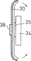
(2) shown in Fig. 4 (b) plane graph and Fig. 4 (b) ' side view, such with first embodiment, with compacting or other method circuit band 30 is bent to arc (J bending), be bonded to semiconductor element 34 with adhesive 35 then.
(3) shown in Fig. 5 (a) plane graph and Fig. 5 (a) ' side view, such with first embodiment, be produced on the semiconductor element 34 and the bonding welding point 36 that is exposed to break-through window 33 by with 37 respective graphical 32 that are electrically connected to circuit band 30 that go between.
(4) shown in Fig. 5 (b) plane graph and Fig. 5 (b) ' side view, such with first embodiment, apply break-through window 33 localized area on every side of circuit band 30 with sealing wire 37 with resin material 38, and, make their clads live semiconductor element 34 with compacting or two sides of other method crooked circuit band 30.
(5) result shown in Fig. 5 (c) plane graph and Fig. 5 (c) ' side view, has just finished the semiconductor device that has the J-shaped warp architecture.
Because semiconductor element 34 is enclosed among the circuit band 30, so on being installed in unshowned circuit board the time, the mechanical strength of the semiconductor device of the 3rd embodiment just is improved.
The semiconductor device that semiconductor device is enclosed in the 3rd embodiment in the metal circuit band has also improved shielding action, can improve electrology characteristic, and has improved mechanical strength, in the time of on being installed in circuit board, can provide higher reliability.
The 4th embodiment
The manufacture process of the semiconductor device of fourth embodiment of the invention is described with reference to Fig. 6.
(1) shown in Fig. 6 (a) plane graph and Fig. 6 (a) ' side view, this process starts from making a semiconductor device 40 with the method that is same as the 3rd embodiment.Its figure is represented with 40A.
(2) shown in Fig. 6 (b), semiconductor device 40 is installed to circuit board 41 securely with the bonding method that welds glue 42 and so on.Method with weldering glue 42 and so on uses the semiconductor device made from quadrat method 40 to be installed on the semiconductor device 40 another.If needed, can a folded ground be installed by one or more identical semiconductor device, thereby form the semiconductor device tower.
Be welded to connect in the semiconductor device 40 of semiconductor element 34, the four embodiment and be joined to one another by means of when being installed in circuit board 41, being produced on figure 40A on the circuit band 30.
It is that work capacity can be improved that the 4th embodiment makes the quantity of the semiconductor device on the limited circuit board space.This just provides with conventional dual in-line package semiconductor device stacking identical effect has been installed.The structure of this embodiment semiconductor device thereby more more superior than the CSP structure of the regulation of conventional semiconductor device.
The 5th embodiment
Fig. 7 shows the manufacture process of the semiconductor device of fifth embodiment of the invention.
(1) this process starts from preparing a circuit band 50 that for example is made of metal, shown in Fig. 7 (a) plane graph and Fig. 7 (a) ' side view, on an one side, be manufactured with the window 53 of an insulating barrier 51 and a series of figure 52 and one of them break-through, and be connected in semiconductor element 54 with adhesive 55.The figure 52 usefulness lead-in wire 57 of circuit band 50 is electrically connected on the corresponding bonding welding point 56 that is produced on semiconductor element 54 and is exposed to break-through window 53.
(2) the same with first embodiment, apply circuit band 50 break-through windows 53 localized areas on every side with sealing wire 57 with resin material 58.Then, the same with the 3rd embodiment shown in Fig. 7 (b) plane graph and Fig. 7 (b) ' side view, with suppressing or other method curves two sides of circuit band 50 L shaped, make them encase semiconductor element 54.
(3) shown in Fig. 7 (c) plane graph and Fig. 7 (c) ' side view, on figure 52, make by for example welding after the electrode 59 that glueballs forms, just finished semiconductor device.
The 5th embodiment is used to device is arranged on the unshowned circuit board by the electrode 59 formed of weldering glueballs, thereby semiconductor device can be complementary with the desired counterflow condition of the ball grid array semiconductor device of knowing that installation is widely used as multitube pin logical device.
The semiconductor device of the 5th embodiment thereby be suitable for being installed to the desired counterflow condition of circuit board, and the figure that makes its circuit band can be used for checking completion (promptly welding glueballs is connected) electrology characteristic afterwards, is damaged (for example being out of shape owing to pressing probe) thereby prevent to weld glueballs.And figure is used to check that the semiconductor device downside (weldering glueballs) that may be difficult to see promptly conducts electricity situation to the bonding conditions of circuit board, thereby guarantees more high-grade installation.
As a result, the surface mount type semiconductor device of the first, second, third and the 5th embodiment can be installed on any circuit board (not shown) easily according to the present invention.
Though the most preferred embodiment according to semiconductor and manufacture method thereof has been described the present invention, the present invention is not limited to these embodiment.Person skilled in the art know, can make various changes and correction and do not surmount the explanation of the present invention and the technical characterstic of claims defined and belong to scope of the present invention.
As mentioned above, the invention provides a kind of novelty improvement surface mount type semiconductor device (but its simple in structure and high-density installation), a kind of utensil and a kind of method of making semiconductor device that semiconductor device is installed.
The Japanese patent application No.9-27424's that on February 12nd, 1997 was proposed is whole open herein, comprises specification, claim, accompanying drawing and general introduction, all intactly herein as list of references.
Claims (20)
1. semiconductor device is characterized in that:
Make and have the circuit band that it protrudes figure;
Be fixedly connected on the semiconductor element of circuit band; And
Respectively the solder joint on the semiconductor element is electrically connected on the circuit band respective graphical and seals with lead-in wire with resin material.
2. according to the semiconductor device of claim 1, circuit band wherein has the window of break-through in an one zone, and the solder joint on the semiconductor element is exposed to wherein in connection.
3. according to the semiconductor device of claim 1, circuit band wherein is equipped with rib.
4. according to the semiconductor device of claim 1, semiconductor element wherein is by two side clads of circuit band.
5. according to the semiconductor device of claim 4, semiconductor element wherein is by two side clads of circuit band, and electrode is produced on the figure.
6. semiconductor device mounted apparatus, it comprises a circuit board that semiconductor device is installed on it, and the feature of above-mentioned semiconductor device is:
Make the circuit band of the figure that has its protrusion;
Be fixedly connected on the semiconductor device of circuit band; And
Respectively the solder joint on the semiconductor is electrically connected on the circuit band respective graphical and seals with lead-in wire with resin material.
7. according to the semiconductor device mounted apparatus of claim 6, circuit band wherein has the window of break-through in an one zone, and the solder joint on the semiconductor element is exposed to wherein in connection.
8. according to the semiconductor device mounted apparatus of claim 6, circuit band wherein is equipped with rib.
9. according to the semiconductor device of claim 1, semiconductor element wherein is by two side clads of circuit band.
10. according to the semiconductor device mounted apparatus of claim 6, semiconductor element wherein is by the side clad of circuit band, and electrode is produced on the figure.
11. semiconductor device mounted apparatus, it comprises a circuit board, utilizes figure with a semiconductor device to be connected to another semiconductor device and one of a plurality of semiconductor device of definition in the claim 5 are stacked on another are installed on the circuit board.
12. a semiconductor device, it comprises:
Be manufactured with the semiconductor element of electrode on the one side;
The circuit band, one is manufactured with conductive pattern on the side, and opposite side is bonded to semiconductor element with corresponding to exposed electrodes;
Be electrically connected on the lead-in wire between electrode and the conductive pattern respectively; And
Seal the encapsulant of these electrodes and lead-in wire.
13. according to the semiconductor device of claim 12, conductive pattern wherein extends between the protrusion district and electrode bonding pad of circuit band.
14. according to the semiconductor device of claim 12, two sides of circuit band extend through semiconductor element wherein and inboard, and its each conductive pattern extends to the inboard of semiconductor element from the electrode bonding pad of circuit band.
15. the manufacture method of a semiconductor device, it comprises the following step:
The figure of circuit band is protruded;
Semiconductor element is bonded to the circuit band; And
With lead-in wire the solder joint on the semiconductor element is electrically connected on the circuit band on the corresponding figure, and seals with resin material.
16. the manufacture method according to the semiconductor device of claim 15 also comprises the step with two side clad semiconductor elements of circuit band.
17. the manufacture method according to the semiconductor device of claim 16 also is included in the step of making electrode on the figure of circuit band.
18. also comprise a folded ground step of using a plurality of semiconductor device that make with quadrat method is installed according to the manufacture method of the semiconductor device of claim 15.
19. a semiconductor device, it comprises:
The semiconductor chip that on chip surface, has a plurality of solder joints;
Be fixed in lip-deep circuit band, this surface is gone up and to be had exposed region at the solder joint place, and has a plurality of and electrodes that with solder joint be connected corresponding with solder joint; And
Make solder joint expose the encapsulant of a part of electrode.
20. according to the semiconductor device of claim 19, wherein said circuit band comprises metal, be produced on the insulating barrier on the metal and be produced on conductive pattern on the insulating barrier.
Applications Claiming Priority (2)
| Application Number | Priority Date | Filing Date | Title |
|---|---|---|---|
| JP027424/97 | 1997-02-12 | ||
| JP02742497A JP3499392B2 (en) | 1997-02-12 | 1997-02-12 | Semiconductor device |
Publications (1)
| Publication Number | Publication Date |
|---|---|
| CN1191389A true CN1191389A (en) | 1998-08-26 |
Family
ID=12220736
Family Applications (1)
| Application Number | Title | Priority Date | Filing Date |
|---|---|---|---|
| CN98104089A Pending CN1191389A (en) | 1997-02-12 | 1998-02-10 | Semiconductor device, semiconductor device mounted appliance, and method of producing semiconductor device |
Country Status (7)
| Country | Link |
|---|---|
| US (1) | US6198160B1 (en) |
| EP (1) | EP0859411B1 (en) |
| JP (1) | JP3499392B2 (en) |
| KR (1) | KR19980070133A (en) |
| CN (1) | CN1191389A (en) |
| DE (1) | DE69712596T2 (en) |
| TW (1) | TW348304B (en) |
Families Citing this family (5)
| Publication number | Priority date | Publication date | Assignee | Title |
|---|---|---|---|---|
| JP2003258180A (en) * | 2002-02-27 | 2003-09-12 | Sanyo Electric Co Ltd | Method for manufacturing semiconductor device |
| WO2005104230A1 (en) * | 2004-04-23 | 2005-11-03 | Nec Corporation | Wiring board, semiconductor device and wiring board manufacturing method |
| WO2009056992A2 (en) * | 2007-11-01 | 2009-05-07 | Schlumberger Canada Limited | Reservoir fracture simulation |
| US8188587B2 (en) * | 2008-11-06 | 2012-05-29 | Fairchild Semiconductor Corporation | Semiconductor die package including lead with end portion |
| CN103167729B (en) * | 2013-02-25 | 2016-01-20 | 合肥京东方光电科技有限公司 | Flexible printed circuit board and display unit |
Family Cites Families (29)
| Publication number | Priority date | Publication date | Assignee | Title |
|---|---|---|---|---|
| US3930115A (en) * | 1971-05-19 | 1975-12-30 | Philips Corp | Electric component assembly comprising insulating foil bearing conductor tracks |
| US4155615A (en) * | 1978-01-24 | 1979-05-22 | Amp Incorporated | Multi-contact connector for ceramic substrate packages and the like |
| US4147889A (en) * | 1978-02-28 | 1979-04-03 | Amp Incorporated | Chip carrier |
| US4398235A (en) * | 1980-09-11 | 1983-08-09 | General Motors Corporation | Vertical integrated circuit package integration |
| US4673967A (en) * | 1985-01-29 | 1987-06-16 | Texas Instruments Incorporated | Surface mounted system for leaded semiconductor devices |
| DE68927295T2 (en) * | 1988-07-08 | 1997-05-07 | Oki Electric Ind Co Ltd | SYNTHETIC-SEALED SEMICONDUCTOR COMPONENT |
| DE3911711A1 (en) | 1989-04-10 | 1990-10-11 | Ibm | MODULE STRUCTURE WITH INTEGRATED SEMICONDUCTOR CHIP AND CHIP CARRIER |
| US5200364A (en) * | 1990-01-26 | 1993-04-06 | Texas Instruments Incorporated | Packaged integrated circuit with encapsulated electronic devices |
| JPH03227541A (en) * | 1990-02-01 | 1991-10-08 | Hitachi Ltd | Semiconductor device |
| US5583375A (en) | 1990-06-11 | 1996-12-10 | Hitachi, Ltd. | Semiconductor device with lead structure within the planar area of the device |
| US5053852A (en) * | 1990-07-05 | 1991-10-01 | At&T Bell Laboratories | Molded hybrid IC package and lead frame therefore |
| US5148265A (en) | 1990-09-24 | 1992-09-15 | Ist Associates, Inc. | Semiconductor chip assemblies with fan-in leads |
| KR920007132A (en) * | 1990-09-24 | 1992-04-28 | 엔. 라이스 머레트 | Insulated lead frame for integrated circuit and manufacturing method thereof |
| KR100234824B1 (en) * | 1991-03-20 | 1999-12-15 | 윌리엄 비. 켐플러 | Semiconductor devices |
| JPH05102245A (en) * | 1991-10-11 | 1993-04-23 | Nippon Steel Corp | Semiconductor device and manufacture thereof |
| US5350947A (en) | 1991-11-12 | 1994-09-27 | Nec Corporation | Film carrier semiconductor device |
| EP0598914B1 (en) * | 1992-06-05 | 2000-10-11 | Mitsui Chemicals, Inc. | Three-dimensional printed circuit board, electronic circuit package using this board, and method for manufacturing this board |
| JP3088193B2 (en) * | 1992-06-05 | 2000-09-18 | 三菱電機株式会社 | Method for manufacturing semiconductor device having LOC structure and lead frame used therein |
| US5375041A (en) * | 1992-12-02 | 1994-12-20 | Intel Corporation | Ra-tab array bump tab tape based I.C. package |
| US5399902A (en) | 1993-03-04 | 1995-03-21 | International Business Machines Corporation | Semiconductor chip packaging structure including a ground plane |
| KR970000214B1 (en) * | 1993-11-18 | 1997-01-06 | 삼성전자 주식회사 | Semiconductor device and method of producing the same |
| JPH088389A (en) * | 1994-04-20 | 1996-01-12 | Fujitsu Ltd | Semiconductor device and semiconductor device unit |
| US5747874A (en) * | 1994-09-20 | 1998-05-05 | Fujitsu Limited | Semiconductor device, base member for semiconductor device and semiconductor device unit |
| US5600179A (en) * | 1994-09-27 | 1997-02-04 | Nec Corporation | Package for packaging a semiconductor device suitable for being connected to a connection object by soldering |
| JP3475306B2 (en) | 1994-10-26 | 2003-12-08 | 大日本印刷株式会社 | Method for manufacturing resin-encapsulated semiconductor device |
| DE9417734U1 (en) | 1994-11-08 | 1995-03-16 | Zentrum Mikroelektronik Dresden GmbH, 01109 Dresden | Semiconductor arrangement for chip modules |
| US5674785A (en) * | 1995-11-27 | 1997-10-07 | Micron Technology, Inc. | Method of producing a single piece package for semiconductor die |
| JPH09186286A (en) * | 1996-01-05 | 1997-07-15 | Matsushita Electron Corp | Lead frame and mounting method for semiconductor chip |
| US5783857A (en) * | 1996-07-25 | 1998-07-21 | The Whitaker Corporation | Integrated circuit package |
-
1997
- 1997-02-12 JP JP02742497A patent/JP3499392B2/en not_active Expired - Fee Related
- 1997-08-19 TW TW086111829A patent/TW348304B/en not_active IP Right Cessation
- 1997-10-22 US US08/955,817 patent/US6198160B1/en not_active Expired - Fee Related
- 1997-12-04 KR KR1019970065946A patent/KR19980070133A/en active Search and Examination
- 1997-12-12 DE DE69712596T patent/DE69712596T2/en not_active Expired - Fee Related
- 1997-12-12 EP EP97121955A patent/EP0859411B1/en not_active Expired - Lifetime
-
1998
- 1998-02-10 CN CN98104089A patent/CN1191389A/en active Pending
Also Published As
| Publication number | Publication date |
|---|---|
| JP3499392B2 (en) | 2004-02-23 |
| EP0859411A2 (en) | 1998-08-19 |
| EP0859411A3 (en) | 1999-03-17 |
| DE69712596T2 (en) | 2003-01-02 |
| DE69712596D1 (en) | 2002-06-20 |
| JPH10223671A (en) | 1998-08-21 |
| KR19980070133A (en) | 1998-10-26 |
| EP0859411B1 (en) | 2002-05-15 |
| TW348304B (en) | 1998-12-21 |
| US6198160B1 (en) | 2001-03-06 |
Similar Documents
| Publication | Publication Date | Title |
|---|---|---|
| CN1118097C (en) | Semiconductor device and method of manufacturing the same | |
| KR100470897B1 (en) | Method for manufacturing dual die package | |
| CN1041254C (en) | Semiconductor device and a manufacturing method therefor | |
| CN1127764C (en) | wiring part and lead frame with same | |
| JP2520575B2 (en) | Resilient lead for electrically and mechanically connecting an integrated circuit chip package to a surface of a substrate and method of manufacturing the same | |
| EP1168440A1 (en) | Semiconductor device having an improved structure for preventing cracks, improved small-sized semiconductor and method of manufacturing the same | |
| CN1091301C (en) | Semiconductor device | |
| CN1254859C (en) | Manufacturing method of circuit device | |
| CN1043828A (en) | The manufacture method of semiconductor device | |
| CN1289147A (en) | Semiconductor device packaged by resin | |
| CN1650410A (en) | Partially patterned lead frames and methods of making and using the same in semiconductor packaging | |
| CN1174403A (en) | Chip-Size semiconductor package and fabrication method thereof | |
| CN1816249A (en) | Circuit board | |
| CN1320965A (en) | Semiconductor package and mfg. method thereof | |
| CN1591841A (en) | Tape circuit substrate and semiconductor chip package using the same | |
| CN1815726A (en) | Circuit board and manufacturing method therefor and semiconductor package and manufacturing method therefor | |
| CN1197290A (en) | Semiconductor device | |
| JP2904141B2 (en) | Semiconductor device | |
| CN1191389A (en) | Semiconductor device, semiconductor device mounted appliance, and method of producing semiconductor device | |
| JP4635471B2 (en) | Semiconductor device and manufacturing method thereof, mounting structure of semiconductor device, and lead frame | |
| CN100352319C (en) | Circuit board with pin made of resin | |
| CN1139984C (en) | semiconductor device, assembling method, and circuit baseboard and soft baseboard and mfg. method therefor | |
| CN1722422A (en) | Semiconductor packages | |
| CN1256515A (en) | Semiconductor device with grid ball bonded array structure and its manufacturing method | |
| JP4038021B2 (en) | Manufacturing method of semiconductor device |
Legal Events
| Date | Code | Title | Description |
|---|---|---|---|
| C06 | Publication | ||
| PB01 | Publication | ||
| C10 | Entry into substantive examination | ||
| SE01 | Entry into force of request for substantive examination | ||
| C02 | Deemed withdrawal of patent application after publication (patent law 2001) | ||
| WD01 | Invention patent application deemed withdrawn after publication |