The setting and the wiring method that are used for SIC (semiconductor integrated circuit)
The present invention relates to be used for the setting and the wiring method of semiconductor devices, and especially relate to the setting and the wiring method of the SIC (semiconductor integrated circuit) of a kind of Aided Design that uses a computer (being abbreviated as CAD).
When using CAD to carry out topological design, need be to comprising phase inverter, designing with each different types of elementary cell of non-(circuit) or non-(circuit).In the case, say generally in same elementary cell that a plurality of transistors size to each other of forming elementary cell is different, this is by the circuit characteristic decision of single elementary cell.Therefore in the prior art, adopted a kind of like this method for designing, promptly at first preparing required species number purpose elementary cell also is parameterized units, gives birth to required unit from movable property during with box lunch input design rule, transistor size and other condition.
Being used for of prior art realizes that the setting of parameterized units above-mentioned and wiring method comprise following two methods: be provided with and wiring method at first kind, only transistor be set at target, and will connect up conductor and connection are described with relational expression; In second kind of setting and wiring method, transistor is described to target, and only expresses the relevant position between the transistor target, and the wiring between target is carried out automatically according to link information.
At first, explain the notion of transistor target in conjunction with the Fig. 1 that schematically describes the transistor target.The transistor target is not consider the transistor pattern form of transistor size as a device by describing, and comprise grid, the empty endpoint location of source electrode and drain electrode, TG, TS, and TD door, transistor size L (length) and W (width) and reference position (point) OXY express.
The setting and the wiring method of first prior art are described with reference to the process flow diagram of figure 2 now.At first, in step p1, the parameter of transistor size is used as the transistor target and sets, and then, describes the relational expression between transistor target and wiring conductor and contact.Forming according to the pattern of having located and design rule determines to prepare under the situation of position location and cloth line position the expression formula of being correlated with.In addition, wiring is described and is comprised and the relevant information of determined wiring conductor layer, and the contact description comprises the linkage unit name that will be positioned.
In step P2, determine the first transistor day target reference position, and in step P4, produce and the fixed position of orientated seed body according to relevant expression formula is next, determine in step P5 that perhaps the position of wiring conductor reaches the position of determining tie point in step P6.In step P3, check whether Place object is the transistor target, if Place object is the transistor target, program enters into step P4, in step P4, produce transistor, and on the basis of correlated expression formula, come definite transistorized position that is provided with that is produced according to given parameter.On the other hand, if Place object is the wiring conductor, program enters into step p5, calculates the starting point and the end point of wiring conductor in step p5 according to the correlated expression formula, and by using specified wiring conductor layer to connect up.In addition, if Place object is a contact, program enters into step p6, comes the compute location position according to the correlated expression formula in step p6, and locatees specified junction unit.The full content of describing in this routine processes correlated expression formula.
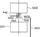
Now, describe the specific embodiment of this technology with reference to figure 3A, Fig. 3 A shows the wiring diagram of location/wiring object element and Fig. 3 B shows the identical situation by transistor target correlated expression formula.Transistor Q1 shown in Fig. 3 A and Q2 represent with transistor target Q01 and the Q02 shown in Fig. 3 B respectively.Wiring conductor W1, W2, W3, W4 and W5 shown in Fig. 3 A represents that with wiring conductor W01, W02, W03, W04 and the W05 shown in Fig. 3 B it has represented the center line in path respectively.Contact TH1 shown in Fig. 3 A and TH2 represent with contact TH01 and the TH02 shown in Fig. 3 B respectively.
For example, under the situation of location wiring conductor W02, be necessary to determine end points P21 and P22.If located transistor target Q01, spaced apart according to design rule, with the x coordinate setting of end points P22 wiring conductor W01 and transistor target Q01 separate location, and the Y coordinate of end points p22 is positioned in by the position that conductor W02 and transistor target Q01 separate of will connecting up, the interval of design rule by the interval of design rule.The Y coordinate of end points P21 is identical with the Y coordinate of end points P22, and the X coordinate of end points p22 is identical with the X coordinate of the end points T26 of transistor target Q02.
Therefore, after handling wiring conductor W04, contact TH2 and transistor target Q02 and having determined the end points T26 of transistor target Q02, this x coordinate of end points P22 and Y coordinate just can have been obtained, at last, with the wiring conductor layer of appointment and the wiring conductor width of appointment end points P21 and P22 are interconnected.
In the setting and wiring method of this first prior art, in the situation of determining wiring conductor W02, must consider not the endpoint location of the transistor target Q02 that directly links to each other with wiring conductor W02, in other words, at the wiring conductor that does not directly link to each other with the end points of transistor target, the essential influence of considering all endpoint locations, and the sequence of positions of definite wiring order and transistor target are so that introduce them in the relevant expression formula.This has just finished relevant expression formula, and when transistor size is very big, is easy to ignore the suffered influence of wiring conductor.
In addition, for setting and the wiring method of realizing first prior art, the common practice is that a unit generator program is all described in each unit, therefore, can not preserve the data of each unit, and and then the very difficult element that changes the unit.
With reference now to the process flow diagram of Fig. 4, the setting and the wiring method of second prior art are described.At first, in step R1, the parameter of transistor size is used as the transistor target and sets, and then, specifies the relative position between the transistor target.Then, in step R2, generate transistor according to the transistorized parameter of in relevant location information, describing.After this, in step R3, determine the position location (original position) of the first transistor target, and in step R4, locate the transistor that is generated according to the relevant position of in relevant location information, describing.At this moment, regulate to avoid transistorized overlapped.Then, in step R5,, carried out being decided connecting wiring between the transistor of position by using diffusion layer, polysilicon layer and aluminium wiring layer according to link information.
This wiring is at first to carry out according to the sharing transistor that uses diffusion layer, then, is connected with the aluminium wiring layer by using polysilicon wiring layer.At this moment, when needs connect the wiring layer of Different Plane, a contact just need be set to satisfy design rule.In addition, if crystal do not exist for the wiring conductor required interval, then carry out the processing that transistor is expanded at interval.
Describe the instantiation of this physical process referring now to Fig. 5 A, Fig. 5 A shows the wiring diagram that will locate/connect up object element and Fig. 5 B shows the relevant position according to the unit of the correlated expression formula of transistor target.Transistor Q3, Q4 shown in Fig. 5 A and Q5 represent with transistor target Q03, Q04 and Q05 among Fig. 5 B respectively, and Fig. 5 B shows these transistorized relative position relations.
At first, generate transistor, and the transistor target that is generated is promptly not overlapped each other between transistor by with a kind of like this method location according to size L and the W of each transistor target Q03, Q04 and Q05.Then, according to link information, the diffusion layer of transistor target Q03, Q04 and Q05 to possible degree, then, is carried out connection between transistor terminal by using polysilicon wiring layer and aluminium wiring layer by socialization.At this moment, when wiring layer being connected to each other, then being provided with one and connecting contact on different planes.
If wiring space is not enough in the step that generates wiring conductor W15 and W14 and contact TH3 and TH4, then expand the interval between transistor target Q05 and transistor target Q03 and Q04 to required degree.At last, obtain the wiring shown in Fig. 5 A.
Yet in the location and wiring method of this second technology, for example, when the channel length L of transistor Q5 is extended, might by around or circular circuit generated wiring conductor W14 and W13 to keep away transistor Q3 and Q4, using wiring conductor W14A and the W13A shown in Fig. 5 C, during the represented wiring figure of W13B and W13C and contact TH23 and TH24, consequently can produce necessity with the wiring interconnection of conductors of Different Plane.Be considerable in the process of the pricing of this routing path in self routing technology.If produced the wiring conductor of ring-type circuit, it is big that circuit area becomes, and increased extra wiring capacitance.
In addition, for location and the wiring method of realizing second prior art, then need large-sized auto-placement tool and so-called condensing routine.
As mentioned above, the location of first kind of prior art and the shortcoming of wiring method are, it need consider the influence for the endpoint location of the transistor target of all wiring conductors that comprise the wiring conductor that does not directly link to each other with the end points of transistor target, if necessary, for they being introduced wiring order and the tab order that also will determine the transistor target in the relevant expression formula.Therefore, when transistor size was very big, it is very complicated that relevant expression formula becomes, and it is easy to ignore the suffered influence of wiring conductor.
In addition, the essential unit generator program of describing each unit, and thereby, the impossible legacy data that keeps each unit.Its result, the very difficult component that limits the unit for example can't change some transistorized sizes.
On the other hand, the location of second kind of prior art and the shortcoming of wiring method are, because self routing when transistor size changes, will produce the line layout of annular, this can increase circuit area and wiring capacitance.
In addition, for location and the wiring method of realizing second kind of prior art, just need large-sized auto-placement tool and so-called condensing routine.
Correspondingly, provide a kind of setting and wiring method that is used for SIC (semiconductor integrated circuit) in a purpose of inventing, it can overcome the defective in the classic method above-mentioned.
Another object of the present invention provides a kind of setting and wiring method that is used for SIC (semiconductor integrated circuit), and it can reduce the number of wires design step, keeps forming the relative position of member simultaneously.
Above-mentioned and other purpose of the present invention is that setting and the wiring method that is used for SIC (semiconductor integrated circuit) according to the present invention realized, this SIC (semiconductor integrated circuit) has transistorized circuit component or the circuit function block that is included on the semi-conductor chip, be used for generating automatically the desired parameters unit, be provided with and wiring method is to realize that by providing the design information that design rule and comprises transistor size this method comprises:
Be used to prepare to describe as each transistor of transistor target and as the goal description step of the goal description of each wiring conductor of cloth line target, it comprise each target be adjacent target relation relative position information and represent the link information of the connection endpoint of each target.
Transistor target processing step, it is used for generating the transistor positional information that also consideration is relevant according to goal description and locatees the transistor that is generated;
Wiring target processing step, it determines that by the positional information of considering to be correlated with each cloth line target is at in-plane and in the position of vertical direction;
The target endpoint determining step, it is used for determining the rearmost position of each transistor target and the final starting point and the last terminating point of each cloth line target; And
Wiring back one treatment step, it is used for coming each cloth line target is connected up by specified wiring layer.
By the description meeting of most preferred embodiment of the present invention being had clearer understanding to the above and other purpose of the present invention, characteristics and advantage below in conjunction with respective drawings.
Fig. 1 is the synoptic diagram of the notion of description transistor target;
Fig. 2 is the process flow diagram of an example of the setting of describing first kind of prior art and wiring method;
Fig. 3 A is the wiring diagram of the unit that will be positioned and connect up;
Fig. 3 B is the correlated expression formula according to the transistor target of the setting of first kind of prior art and wiring method;
Fig. 4 is the process flow diagram of an example of the setting of describing second kind of prior art and wiring method;
Fig. 5 A illustrates the wiring diagram of the unit that will be positioned and connect up;
Fig. 5 B has described the correlated expression formula according to the transistor target of the setting of second kind of prior art and wiring method;
Fig. 5 C is the wiring diagram of the result of the setting of second kind of prior art and wiring method;
Fig. 6 is the process flow diagram according to first embodiment of setting of the present invention and wiring method;
Fig. 7 A and 7B have described according to the notion of wiring Target Setting of the present invention and wiring method;
Fig. 8 has described according to relation and wiring method between the cloth line target in of the present invention the setting;
Fig. 9 A has described according to each the target processing flow process that goes on foot of joining in setting of the present invention and the wiring method to 9E;
Figure 10 A is used to describe the operation according to second embodiment of setting of the present invention and wiring method to the notion that 10B shows the cloth line target.
With reference to figure 6, it shows the process flow diagram of first embodiment of arranged according to the present invention and wiring method
According to first embodiment, in goal description step S1, whole elementary cells that will produce are described with transistor target and cloth line target according to setting of the present invention and wiring method.In each transistor target, the link information of connection endpoint of transistor size, expression related transistor target and the parameter of or left and right adjacent target upper and lower have been specified with the related transistor target.
Then, come the notion of cloth line target is described with reference to figure 7A and 7B, it has schematically described the cloth line target.The cloth line target comprises the plane routing target of expression plane routing conductor as shown in Figure 7A, and vertically the connect up vertical cloth line target of conductor of expression as shown in Fig. 7 B.Each cloth line target partly is made up of the line with 2 opposite end points and is had about about the link information of wiring layer two-end-point and about the information of the up and down of ST and SB or SL and SR or a left side and right adjacent situation.And in target endpoint determining step S6, determine these end points.
Wiring layer of plane routing object representation as shown in Figure 7A, on wiring layer, have the line part 1 of two relative end P11 and P12, with upward to adjacent states ST and the direction represented of the state SB adjacent with downward direction on the adjacent target 11 adjacent and 12 and CN11 of link information separately and the CN12 of end points P11 and P12 with the plane routing target.
On the other hand, vertical cloth line target as shown in Fig. 7 B has been specified wiring layer, on the line part 2 that has two opposite endpoint P21 and P22 on the wiring layer, adjacent state SL and dextrad adjacent states SR represent with left direction direction with the vertical adjacent adjacent target 21 and 22 of cloth line target, and each link information CN21 and CN22 of end points P21 and P22.
In each plane and vertical cloth line target, when not specifying an adjacent target, think that then wiring conductor coordinate extends to the connection endpoint position.
If the wiring layer of cloth line target is different from the wiring layer of connection endpoint, when being provided with a through hole type contact that is used for connecting between different wiring layers, then determined a target that does not need to consider neighbouring relations.For example, illustrated among Fig. 7 B one be used between different wiring layers and the upper and lower, left and right adjacent states CT of contact TH21, CB, CL, CR between the contact TH21 that connects.
With reference now to Fig. 8, concrete relationship by objective (RBO) is described, its with the formal description of relationship by objective (RBO) figure the wire structures among Fig. 3 A.In Fig. 8, with those the similar or corresponding elements shown in Fig. 3 B with identical reference symbol or numerical code expression, and neighbouring relations arrow curve representation.
Shown wiring comprises transistor target Q01 and Q02, plane routing target W02, W04 and W05 and vertical cloth line target W01 and W03.
Transistor target Q02 is adjacent with plane routing target W04 and link to each other with plane routing target W04 and vertical cloth line target W03 on downward direction.In addition, transistor size L and the W of transistor target Q02 have been set.
Plane routing target W02 is adjacent with transistor target Q01 on downward direction, and links to each other with vertical cloth line target W01 and W03.In addition, and the wiring layer of definite plane routing target W02 be the ground floor aluminium lamination.
Get back to Fig. 6, in step 2, determine the transistorized original position that at first is provided with, and in step 3, the kind of target is distinguished with the order of as shown in Figure 8 number of targets.As the result who distinguishes, program enters into or transistor target processing step S4 or wiring target processing step S5, perhaps enters into wiring back one treatment step S7 when driftlessness exists.
In transistor target processing step S4, produce transistor according to specified transistor size, if determine no position adjacent, then the transistor that is generated is placed in initial original position.If define adjacent state, then with on or down the position that separates of intended target determine Y one coordinate by the determined required interval of principle of design (design rule at interval), and determining X one coordinate by principle of design with a left side or the position that separates of right intended target, after this, the transistor that is generated is arranged on the indicated position of definite thus Y one coordinate and X one coordinate.Yet if determine publicly-owned related transistorized diffusion layer, transistor is by adjacent setting with the transistor of having located, and this transistor of having located has the designated and related publicly-owned diffusion layer of transistorized diffusion layer.
In wiring target processing step S5, if on specifying/following position adjacent state then according to link information with Y one coordinate of determined plane routing target Y one coordinate as the terminal location of the target of having located.If specify have on/adjacent position down, will go up by the principle of design interval by handling a processing procedure similar/Y one coordinate of plane routing target is determined in the position that following adjacent target is separated with the adjacent states processing of transistor target.
Under the situation of vertical cloth line target, when having specified a nothing left side/right adjacent states, then according to link information and akin X one coordinate of determining vertical cloth line target of plane routing target.If specify there to be the adjacent state in a left side/right side, then with on/X one coordinate of vertical cloth line target is determined in the position that following adjacent target is separated at interval by design rule.
After finishing the target processing process, in target endpoint determining step S6, determine the endpoint location of target at every turn.Because the distance of the terminal location of transistorized original position and transistorized three terminals is known in advance, can calculate the terminal position of transistor target by transistorized position location.When the cloth line target that will link to each other with the transistor target had been positioned, under the situation of plane routing target, X one coordinate of the connection end point of plane routing target became X one coordinate of the connection end point of transistor target.Under the situation of vertical cloth line target, vertically Y one coordinate of the connection end point of cloth line target becomes Y one coordinate of the connection end point of transistor target.
In addition, owing in wiring target processing step S5, determined Y one coordinate position of the connection end point of plane routing target, when wanting connected target to be positioned, X one coordinate of the connection end point of plane routing target becomes X one coordinate of the connection end point of the target of having located.Similarly, owing to determined the position of the connection end point of vertical cloth line target, when the target that will connect had been located, vertically Y one coordinate of the connection end point of cloth line target became Y one coordinate of the connection end point of the target of having located.
In addition, the position of the connection end point of the cloth line target that links to each other with another cloth line target be according to carry out for the similar mode of the processing procedure of the cloth line target that links to each other with transistor.
When the plane of the terminating layer of the plane of the terminating layer of each target and connection endpoint not simultaneously, from the contact described in the design rule, selecting the contact of an optimum, and under the situation of the adjacent states of considering connecting point position the selected contact in location.
After the wiring after whole target processing is all finished among the treatment step S7, thereby generate last wiring by determining that wiring layer connects up according to determined cloth line position.
Below, describe the instantiation that the transistor target must be managed step S4, wiring target processing step S5, target endpoint treatment step S6 and wiring back one treatment step S7 with reference to Fig. 9 A to 9E, Fig. 9 A has described when setting according to the present invention and wiring method are applied to by the represented unit of the target figure of Fig. 8 of treatment scheme to(for) target to 9E by the step.
At first, as shown in Fig. 9 A, generate transistor target Q01, and be positioned at determined original position in step S2 according to transistor size.Fig. 9 B has described the situation after plane routing target W02 is processed.Because plane routing target W02 is adjacent with transistor target Q01 on downward direction, separating Y one coordinate that plane routing target W02 is determined in design rule position at interval with transistor target Q01.Plane routing target W02 links to each other with vertical cloth line target W01 and W03.Here, because vertically cloth line target W02 is positioned, vertically X one coordinate of cloth line target W01 is determined.Therefore, finally determined the end points P21 of plane routing target W02.Yet,, therefore can't determine the end points P22 of plane routing target W02 because vertically cloth line target W03 also is not positioned.
Similarly, when plane routing target W04 is processed,, therefore can't determine the end points P41 of plane routing target W04 because transistor target Q02 yet is not positioned.This kind situation has been shown among Fig. 9 C.
Fig. 9 D has described the situation after transistor target Q02 has been positioned.Because transistor target Q02 is adjacent with cloth line target W04 on downward direction, Y one coordinate of transistor target Q02 is determined with cloth line target W04 and separates required design rule at interval.On the other hand, owing to specify a left side/right adjacent states for transistor target Q02, selected X one coordinate of X one coordinate of initial position as transistor Q02.When transistor target Q02 has been positioned, determine X one coordinate of end points P41.In addition, because the plane of cloth line target W04 is different from the plane of the connection end point of transistor target Q02, therefore contact TH2 is set.
Fig. 9 E has described the situation after vertically cloth line target W03 and plane routing target W05 are processed.Because vertically cloth line target W03 does not have specified adjacent states, so the endpoint location of transistor target Q02 is determined X one coordinate as vertical cloth line target W03.In addition, because vertically cloth line target W03 links to each other with plane routing target W02, the final end points P22 that determines vertical cloth line target W02 in this step.
Fig. 9 F has described by coming place of transistor target Q01 and P02 with transistor Q1 and Q2 respectively, and is added to cloth line target W01, W02, W03, W04 and W05 so that the wiring diagram that obtain connecting up conductor W1, W2, W3, W4 and W5 obtain by the wiring conductor width with determined wiring layer and design rule.
Now, describe second embodiment, in Figure 10 A, provide by in identical symbol and number, inserting " O " with corresponding elements shown in Fig. 5 A according to setting of the present invention and wiring method with reference to figure 10A.Figure 10 A is by transistor target Q03, Q04 and Q05 and cloth line target W011, W013, W014, W015, W016, W017 and W019 and the same wiring diagram that shows Fig. 5 A with the adjacent relation of arrow curve representation that adds.Cloth line target W014 is adjacent with transistor target Q03 on downward direction, and cloth line target W013 is adjacent with cloth line target W012 on the direction of on the left side.
Figure 10 B shows the wiring diagram that is obtained when the transistor size L of transistor target Q05 (length) is extended.Because it is definite for the neighbouring relations of cloth line target W014, W013, even cloth line target W014 position (L-R direction) on in-plane move, cloth line target W013 also is positioned at the right side of cloth line target W012, thereby has kept its relative position relation forever.
As can be seen from the above, be used for partly leading not according to of the present invention that the setting and the wiring method of integrated circuit is characterized in that it comprises following steps, a goal description step, it is used to prepare a goal description, this goal description is described each transistor and each wiring conductor as the cloth line target of cloth line target as the transistor target, and comprises also in this goal description that each target is adjacent the relevant location information of target and the link information of each target; Transistor target processing step, it is used for generating each transistor and locating the transistor that is generated according to relevant location information according to goal description; One wiring target processing step, it is used for reaching the position that in the vertical direction is determined each wiring on in-plane; And a target endpoint determining step, be used for determining the final position of each transistor target and the final starting point and the final terminal point of each cloth line target.Therefore, even when the wiring conductor that the location does not directly link to each other with transistor, owing to considered transistorized position, so the description amount can be reduced to the only about half of to 1/5th of prior art example.On the other hand, unless the wiring conductor does not directly link to each other with transistor, otherwise needn't consider transistorized terminal location.In addition, owing to be to describe target simply in order, therefore can reduce the possibility of ignorance, and reduce the number of design procedure.
In addition, compare with automatic step line, the representation of cloth line target makes it might produce desirable wiring figure, therefore, neither can the outer wiring capacitance of plus also can not increase extra cloth line resistance, and its result can produce the wiring with premium properties.
In addition, compare with self routing, the representation of cloth line target can reduce the size of program.Because the information of each elementary cell can be used as data and preserve, therefore can change the composed component of unit at an easy rate.
Here invention has been described in conjunction with specific embodiments, yet, be noted that the present invention is not limited only on the particular content of described structure, and change within the scope of the appended claims and modification all are scope of the present invention.