CN116323184A - Resin film with conductor layer, laminated substrate, and method for producing resin film with conductor layer - Google Patents
Resin film with conductor layer, laminated substrate, and method for producing resin film with conductor layer Download PDFInfo
- Publication number
- CN116323184A CN116323184A CN202280006626.6A CN202280006626A CN116323184A CN 116323184 A CN116323184 A CN 116323184A CN 202280006626 A CN202280006626 A CN 202280006626A CN 116323184 A CN116323184 A CN 116323184A
- Authority
- CN
- China
- Prior art keywords
- resin film
- conductor layer
- liquid crystal
- crystal polymer
- resin
- Prior art date
- Legal status (The legal status is an assumption and is not a legal conclusion. Google has not performed a legal analysis and makes no representation as to the accuracy of the status listed.)
- Pending
Links
Images


Classifications
-
- C—CHEMISTRY; METALLURGY
- C08—ORGANIC MACROMOLECULAR COMPOUNDS; THEIR PREPARATION OR CHEMICAL WORKING-UP; COMPOSITIONS BASED THEREON
- C08J—WORKING-UP; GENERAL PROCESSES OF COMPOUNDING; AFTER-TREATMENT NOT COVERED BY SUBCLASSES C08B, C08C, C08F, C08G or C08H
- C08J5/00—Manufacture of articles or shaped materials containing macromolecular substances
- C08J5/18—Manufacture of films or sheets
-
- H—ELECTRICITY
- H05—ELECTRIC TECHNIQUES NOT OTHERWISE PROVIDED FOR
- H05K—PRINTED CIRCUITS; CASINGS OR CONSTRUCTIONAL DETAILS OF ELECTRIC APPARATUS; MANUFACTURE OF ASSEMBLAGES OF ELECTRICAL COMPONENTS
- H05K1/00—Printed circuits
- H05K1/02—Details
- H05K1/0213—Electrical arrangements not otherwise provided for
- H05K1/0216—Reduction of cross-talk, noise or electromagnetic interference
- H05K1/0218—Reduction of cross-talk, noise or electromagnetic interference by printed shielding conductors, ground planes or power plane
- H05K1/0219—Printed shielding conductors for shielding around or between signal conductors, e.g. coplanar or coaxial printed shielding conductors
-
- B—PERFORMING OPERATIONS; TRANSPORTING
- B32—LAYERED PRODUCTS
- B32B—LAYERED PRODUCTS, i.e. PRODUCTS BUILT-UP OF STRATA OF FLAT OR NON-FLAT, e.g. CELLULAR OR HONEYCOMB, FORM
- B32B15/00—Layered products comprising a layer of metal
- B32B15/04—Layered products comprising a layer of metal comprising metal as the main or only constituent of a layer, which is next to another layer of the same or of a different material
- B32B15/08—Layered products comprising a layer of metal comprising metal as the main or only constituent of a layer, which is next to another layer of the same or of a different material of synthetic resin
- B32B15/09—Layered products comprising a layer of metal comprising metal as the main or only constituent of a layer, which is next to another layer of the same or of a different material of synthetic resin comprising polyesters
-
- B—PERFORMING OPERATIONS; TRANSPORTING
- B32—LAYERED PRODUCTS
- B32B—LAYERED PRODUCTS, i.e. PRODUCTS BUILT-UP OF STRATA OF FLAT OR NON-FLAT, e.g. CELLULAR OR HONEYCOMB, FORM
- B32B15/00—Layered products comprising a layer of metal
- B32B15/20—Layered products comprising a layer of metal comprising aluminium or copper
-
- B—PERFORMING OPERATIONS; TRANSPORTING
- B32—LAYERED PRODUCTS
- B32B—LAYERED PRODUCTS, i.e. PRODUCTS BUILT-UP OF STRATA OF FLAT OR NON-FLAT, e.g. CELLULAR OR HONEYCOMB, FORM
- B32B17/00—Layered products essentially comprising sheet glass, or glass, slag, or like fibres
- B32B17/06—Layered products essentially comprising sheet glass, or glass, slag, or like fibres comprising glass as the main or only constituent of a layer, next to another layer of a specific material
- B32B17/10—Layered products essentially comprising sheet glass, or glass, slag, or like fibres comprising glass as the main or only constituent of a layer, next to another layer of a specific material of synthetic resin
- B32B17/10005—Layered products essentially comprising sheet glass, or glass, slag, or like fibres comprising glass as the main or only constituent of a layer, next to another layer of a specific material of synthetic resin laminated safety glass or glazing
- B32B17/10165—Functional features of the laminated safety glass or glazing
- B32B17/10431—Specific parts for the modulation of light incorporated into the laminated safety glass or glazing
- B32B17/10467—Variable transmission
- B32B17/10495—Variable transmission optoelectronic, i.e. optical valve
- B32B17/10504—Liquid crystal layer
-
- B—PERFORMING OPERATIONS; TRANSPORTING
- B32—LAYERED PRODUCTS
- B32B—LAYERED PRODUCTS, i.e. PRODUCTS BUILT-UP OF STRATA OF FLAT OR NON-FLAT, e.g. CELLULAR OR HONEYCOMB, FORM
- B32B27/00—Layered products comprising a layer of synthetic resin
- B32B27/36—Layered products comprising a layer of synthetic resin comprising polyesters
-
- C—CHEMISTRY; METALLURGY
- C09—DYES; PAINTS; POLISHES; NATURAL RESINS; ADHESIVES; COMPOSITIONS NOT OTHERWISE PROVIDED FOR; APPLICATIONS OF MATERIALS NOT OTHERWISE PROVIDED FOR
- C09K—MATERIALS FOR MISCELLANEOUS APPLICATIONS, NOT PROVIDED FOR ELSEWHERE
- C09K19/00—Liquid crystal materials
- C09K19/04—Liquid crystal materials characterised by the chemical structure of the liquid crystal components, e.g. by a specific unit
- C09K19/38—Polymers
- C09K19/3804—Polymers with mesogenic groups in the main chain
- C09K19/3809—Polyesters; Polyester derivatives, e.g. polyamides
-
- H—ELECTRICITY
- H05—ELECTRIC TECHNIQUES NOT OTHERWISE PROVIDED FOR
- H05K—PRINTED CIRCUITS; CASINGS OR CONSTRUCTIONAL DETAILS OF ELECTRIC APPARATUS; MANUFACTURE OF ASSEMBLAGES OF ELECTRICAL COMPONENTS
- H05K1/00—Printed circuits
- H05K1/02—Details
- H05K1/03—Use of materials for the substrate
- H05K1/0313—Organic insulating material
- H05K1/032—Organic insulating material consisting of one material
- H05K1/0326—Organic insulating material consisting of one material containing O
-
- H—ELECTRICITY
- H05—ELECTRIC TECHNIQUES NOT OTHERWISE PROVIDED FOR
- H05K—PRINTED CIRCUITS; CASINGS OR CONSTRUCTIONAL DETAILS OF ELECTRIC APPARATUS; MANUFACTURE OF ASSEMBLAGES OF ELECTRICAL COMPONENTS
- H05K3/00—Apparatus or processes for manufacturing printed circuits
- H05K3/46—Manufacturing multilayer circuits
- H05K3/4611—Manufacturing multilayer circuits by laminating two or more circuit boards
- H05K3/4626—Manufacturing multilayer circuits by laminating two or more circuit boards characterised by the insulating layers or materials
- H05K3/4632—Manufacturing multilayer circuits by laminating two or more circuit boards characterised by the insulating layers or materials laminating thermoplastic or uncured resin sheets comprising printed circuits without added adhesive materials between the sheets
-
- B—PERFORMING OPERATIONS; TRANSPORTING
- B32—LAYERED PRODUCTS
- B32B—LAYERED PRODUCTS, i.e. PRODUCTS BUILT-UP OF STRATA OF FLAT OR NON-FLAT, e.g. CELLULAR OR HONEYCOMB, FORM
- B32B2305/00—Condition, form or state of the layers or laminate
- B32B2305/55—Liquid crystals
-
- C—CHEMISTRY; METALLURGY
- C08—ORGANIC MACROMOLECULAR COMPOUNDS; THEIR PREPARATION OR CHEMICAL WORKING-UP; COMPOSITIONS BASED THEREON
- C08J—WORKING-UP; GENERAL PROCESSES OF COMPOUNDING; AFTER-TREATMENT NOT COVERED BY SUBCLASSES C08B, C08C, C08F, C08G or C08H
- C08J2367/00—Characterised by the use of polyesters obtained by reactions forming a carboxylic ester link in the main chain; Derivatives of such polymers
- C08J2367/02—Polyesters derived from dicarboxylic acids and dihydroxy compounds
-
- C—CHEMISTRY; METALLURGY
- C09—DYES; PAINTS; POLISHES; NATURAL RESINS; ADHESIVES; COMPOSITIONS NOT OTHERWISE PROVIDED FOR; APPLICATIONS OF MATERIALS NOT OTHERWISE PROVIDED FOR
- C09K—MATERIALS FOR MISCELLANEOUS APPLICATIONS, NOT PROVIDED FOR ELSEWHERE
- C09K19/00—Liquid crystal materials
- C09K19/04—Liquid crystal materials characterised by the chemical structure of the liquid crystal components, e.g. by a specific unit
- C09K2019/0444—Liquid crystal materials characterised by the chemical structure of the liquid crystal components, e.g. by a specific unit characterized by a linking chain between rings or ring systems, a bridging chain between extensive mesogenic moieties or an end chain group
- C09K2019/0448—Liquid crystal materials characterised by the chemical structure of the liquid crystal components, e.g. by a specific unit characterized by a linking chain between rings or ring systems, a bridging chain between extensive mesogenic moieties or an end chain group the end chain group being a polymerizable end group, e.g. -Sp-P or acrylate
-
- H—ELECTRICITY
- H05—ELECTRIC TECHNIQUES NOT OTHERWISE PROVIDED FOR
- H05K—PRINTED CIRCUITS; CASINGS OR CONSTRUCTIONAL DETAILS OF ELECTRIC APPARATUS; MANUFACTURE OF ASSEMBLAGES OF ELECTRICAL COMPONENTS
- H05K2201/00—Indexing scheme relating to printed circuits covered by H05K1/00
- H05K2201/01—Dielectrics
- H05K2201/0104—Properties and characteristics in general
- H05K2201/0116—Porous, e.g. foam
-
- H—ELECTRICITY
- H05—ELECTRIC TECHNIQUES NOT OTHERWISE PROVIDED FOR
- H05K—PRINTED CIRCUITS; CASINGS OR CONSTRUCTIONAL DETAILS OF ELECTRIC APPARATUS; MANUFACTURE OF ASSEMBLAGES OF ELECTRICAL COMPONENTS
- H05K2201/00—Indexing scheme relating to printed circuits covered by H05K1/00
- H05K2201/01—Dielectrics
- H05K2201/0104—Properties and characteristics in general
- H05K2201/0129—Thermoplastic polymer, e.g. auto-adhesive layer; Shaping of thermoplastic polymer
-
- H—ELECTRICITY
- H05—ELECTRIC TECHNIQUES NOT OTHERWISE PROVIDED FOR
- H05K—PRINTED CIRCUITS; CASINGS OR CONSTRUCTIONAL DETAILS OF ELECTRIC APPARATUS; MANUFACTURE OF ASSEMBLAGES OF ELECTRICAL COMPONENTS
- H05K2201/00—Indexing scheme relating to printed circuits covered by H05K1/00
- H05K2201/01—Dielectrics
- H05K2201/0137—Materials
- H05K2201/0141—Liquid crystal polymer [LCP]
-
- Y—GENERAL TAGGING OF NEW TECHNOLOGICAL DEVELOPMENTS; GENERAL TAGGING OF CROSS-SECTIONAL TECHNOLOGIES SPANNING OVER SEVERAL SECTIONS OF THE IPC; TECHNICAL SUBJECTS COVERED BY FORMER USPC CROSS-REFERENCE ART COLLECTIONS [XRACs] AND DIGESTS
- Y02—TECHNOLOGIES OR APPLICATIONS FOR MITIGATION OR ADAPTATION AGAINST CLIMATE CHANGE
- Y02P—CLIMATE CHANGE MITIGATION TECHNOLOGIES IN THE PRODUCTION OR PROCESSING OF GOODS
- Y02P20/00—Technologies relating to chemical industry
- Y02P20/50—Improvements relating to the production of bulk chemicals
- Y02P20/54—Improvements relating to the production of bulk chemicals using solvents, e.g. supercritical solvents or ionic liquids
Landscapes
- Chemical & Material Sciences (AREA)
- Engineering & Computer Science (AREA)
- Microelectronics & Electronic Packaging (AREA)
- Manufacturing & Machinery (AREA)
- Materials Engineering (AREA)
- Organic Chemistry (AREA)
- Crystallography & Structural Chemistry (AREA)
- Health & Medical Sciences (AREA)
- Chemical Kinetics & Catalysis (AREA)
- Medicinal Chemistry (AREA)
- Polymers & Plastics (AREA)
- Physics & Mathematics (AREA)
- Electromagnetism (AREA)
- Laminated Bodies (AREA)
Abstract
Description
技术领域technical field
本发明涉及带导体层的树脂膜、层叠基板和带导体层的树脂膜的制造方法。The present invention relates to a resin film with a conductor layer, a laminated substrate, and a method for producing the resin film with a conductor layer.
背景技术Background technique
作为用于各种电子设备的层叠基板,在专利文献1中公开了一种多层布线基板,其特征在于,该多层布线基板具有接地层或电源层和信号层隔着绝缘层配置的结构,由在厚度方向上空孔率不同的多孔质膜构成绝缘层,并且将该多孔质膜的空孔率高的一侧的面配置于信号层侧。As a laminated substrate used in various electronic devices,
现有技术文献prior art literature
专利文献patent documents
专利文献1:日本特开2003-8233号公报Patent Document 1: Japanese Patent Laid-Open No. 2003-8233
发明内容Contents of the invention
发明要解决的课题The problem to be solved by the invention
在专利文献1所记载的多层布线基板这样的层叠基板中,为了提高高频区域中的介电特性,有时使用如下技术:通过将多孔质膜用于绝缘层,从而与空孔存在量相应地降低绝缘层的介电常数。例如,在专利文献1所记载的多层布线基板中,如专利文献1的实施例中记载的那样,通过使用了包含聚酰亚胺前体的制膜原液的湿式凝固法来进行制膜,进而,进行用于使聚酰亚胺前体加热闭环的热处理,由此形成的多孔质膜被用作绝缘层。In a laminated substrate such as the multilayer wiring substrate described in
本发明人等为了在专利文献1所记载的多层布线基板中进一步提高高频区域中的介电特性,研究了使用液晶聚合物等热塑性树脂作为多孔质膜的构成材料。然而,已知如果想要使用热塑性树脂并利用专利文献1的实施例中记载的方法形成多孔质膜,则热塑性树脂容易分解,或者由于热塑性树脂的粘弹性而难以维持空孔的形状。这样,在专利文献1所记载的多层布线基板中,实现包含热塑性树脂的多孔质膜本身是困难的,因此在进一步提高高频区域中的介电特性的方面存在改善的余地。In order to further improve the dielectric properties in the high-frequency region in the multilayer wiring board described in
本发明是为了解决上述问题而完成的,其目的在于提供一种带导体层的树脂膜,其能够以包含热塑性树脂的构成来提高高频区域中的介电特性。另外,本发明的目的在于提供具有上述带导体层的树脂膜的层叠基板。此外,本发明的目的在于提供上述带导体层的树脂膜的制造方法。The present invention was made to solve the above-mentioned problems, and an object of the present invention is to provide a resin film with a conductor layer capable of improving dielectric properties in a high-frequency region by including a thermoplastic resin. Another object of the present invention is to provide a laminated substrate having the above-mentioned resin film with a conductor layer. Moreover, the object of this invention is to provide the manufacturing method of the said resin film with a conductor layer.
用于解决课题的手段means to solve the problem
本发明的带导体层的树脂膜的特征在于,在层叠方向上具备树脂膜和导体层,所述树脂膜包含热塑性树脂且在内部设置有空孔,所述导体层与上述树脂膜的至少一个主面侧相邻,在上述树脂膜中,在将上述导体层侧的端面的位置设为第1位置、将在上述层叠方向上距上述第1位置的距离恰好为上述树脂膜的厚度的1/3的位置设为第2位置、将在上述层叠方向上朝向与上述第1位置相反的一侧的距上述第2位置的距离恰好为上述树脂膜的厚度的1/3的位置设为第3位置时,上述空孔以上述第1位置与上述第2位置之间的空孔数多于上述第2位置与上述第3位置之间的空孔数的方式侧重存在于上述第1位置与上述第2位置之间。The resin film with a conductor layer according to the present invention is characterized in that it includes a resin film and a conductor layer in the stacking direction, the resin film contains a thermoplastic resin and has holes provided inside, the conductor layer and at least one of the resin films The main surface side is adjacent, and in the above-mentioned resin film, the position of the end surface on the side of the above-mentioned conductor layer is set as the first position, and the distance from the above-mentioned first position in the above-mentioned stacking direction is exactly 1 times the thickness of the above-mentioned resin film. The position of /3 is set as the second position, and the position facing the side opposite to the first position in the above-mentioned lamination direction from the second position is exactly 1/3 of the thickness of the resin film is set as the first position. In the case of the third position, the pores are more concentrated between the first position and the second position in such a manner that the number of pores between the first position and the second position is greater than the number of pores between the second position and the third position. Between the 2nd position above.
本发明的层叠基板的特征在于,具备本发明的带导体层的树脂膜。The multilayer substrate of the present invention is characterized by comprising the resin film with a conductor layer of the present invention.
本发明的带导体层的树脂膜的制造方法的特征在于,具备如下工序:通过以与包含热塑性树脂的树脂膜的至少一个主面侧相邻的方式设置导体层,从而制作层叠体的工序,所述层叠体在层叠方向上具有上述树脂膜和上述导体层;以及通过对上述层叠体进行热处理,从而在上述树脂膜的内部设置空孔的工序,在上述设置空孔的工序中,在上述树脂膜中,在将上述导体层侧的端面的位置设为第1位置、将在上述层叠方向上距上述第1位置的距离恰好为上述树脂膜的厚度的1/3的位置设为第2位置、将在上述层叠方向上朝向与上述第1位置相反的一侧的距上述第2位置的距离恰好为上述树脂膜的厚度的1/3的位置设为第3位置时,以上述第1位置与上述第2位置之间的空孔数多于上述第2位置与上述第3位置之间的空孔数的方式设置侧重存在于上述第1位置与上述第2位置之间的上述空孔。The method for producing a resin film with a conductor layer according to the present invention is characterized in that it includes a step of producing a laminate by providing a conductor layer adjacent to at least one main surface side of a resin film containing a thermoplastic resin, The laminated body has the above-mentioned resin film and the above-mentioned conductor layer in the stacking direction; and a step of providing a hole in the inside of the above-mentioned resin film by heat-treating the above-mentioned laminated body, and in the step of providing the hole, the In the resin film, the position of the end surface on the side of the conductor layer is set as the first position, and the position at which the distance from the first position in the lamination direction is exactly 1/3 of the thickness of the resin film is set as the second position. position, when the position facing the side opposite to the first position in the lamination direction and the distance from the second position is exactly 1/3 of the thickness of the resin film as the third position, the first The number of holes between the position and the second position is greater than the number of holes between the second position and the third position, and the number of holes between the first position and the second position is emphasized. .
发明效果Invention effect
根据本发明,能够提供以包含热塑性树脂的构成能够提高高频区域中的介电特性的带导体层的树脂膜。另外,根据本发明,能够提供具有上述带导体层的树脂膜的层叠基板。此外,根据本发明,能够提供上述带导体层的树脂膜的制造方法。According to the present invention, it is possible to provide a resin film with a conductor layer that can improve dielectric properties in a high-frequency region by including a thermoplastic resin. In addition, according to the present invention, it is possible to provide a laminated substrate having the above-mentioned resin film with a conductor layer. Moreover, according to this invention, the manufacturing method of the said resin film with a conductor layer can be provided.
附图说明Description of drawings
图1是表示本发明的带导体层的树脂膜的一个例子的截面示意图。FIG. 1 is a schematic cross-sectional view showing an example of a resin film with a conductor layer of the present invention.
图2是针对本发明的带导体层的树脂膜的制造方法的一个例子示出制作层叠体的工序的截面示意图。2 is a schematic cross-sectional view illustrating a step of producing a laminate for an example of the method for producing a resin film with a conductor layer according to the present invention.
图3是针对本发明的带导体层的树脂膜的制造方法的一个例子示出制作层叠体的工序的截面示意图。3 is a schematic cross-sectional view illustrating a step of producing a laminate for an example of the method for producing a resin film with a conductor layer according to the present invention.
图4是针对本发明的带导体层的树脂膜的制造方法的一个例子示出制作层叠体的工序的截面示意图。4 is a schematic cross-sectional view illustrating a step of producing a laminate for an example of the method for producing a resin film with a conductor layer according to the present invention.
图5是表示作为本发明的带导体层的树脂膜的一个例子的、与图1不同的例子的截面示意图。FIG. 5 is a schematic cross-sectional view showing an example different from FIG. 1 as an example of the resin film with a conductor layer of the present invention.
图6是表示作为本发明的带导体层的树脂膜的一个例子的、与图1和图5不同的例子的截面示意图。FIG. 6 is a schematic cross-sectional view showing an example of the resin film with a conductor layer according to the present invention, which is different from FIG. 1 and FIG. 5 .
图7是表示本发明的层叠基板的一个例子的截面示意图。Fig. 7 is a schematic cross-sectional view showing an example of a laminated substrate of the present invention.
图8是针对本发明的层叠基板的制造方法的一个例子示出制作带导体层的树脂膜的工序的截面示意图。8 is a schematic cross-sectional view illustrating a step of forming a resin film with a conductor layer for an example of the method of manufacturing a laminated substrate according to the present invention.
图9是针对本发明的层叠基板的制造方法的一个例子示出制作带导体层的树脂膜的工序的截面示意图。9 is a schematic cross-sectional view illustrating a step of forming a resin film with a conductor layer for an example of the method of manufacturing a laminated substrate of the present invention.
图10是针对本发明的层叠基板的制造方法的一个例子示出制作带导体层的树脂膜的工序的截面示意图。10 is a schematic cross-sectional view illustrating a step of forming a resin film with a conductor layer for an example of the method of manufacturing a laminated substrate of the present invention.
图11是针对本发明的层叠基板的制造方法的一个例子示出形成通孔的工序的截面示意图。FIG. 11 is a schematic cross-sectional view illustrating a step of forming a via hole in an example of the method for manufacturing a laminated substrate of the present invention.
图12是针对本发明的层叠基板的制造方法的一个例子示出形成通孔的工序的截面示意图。FIG. 12 is a schematic cross-sectional view illustrating a step of forming a via hole in an example of the method of manufacturing a laminated substrate of the present invention.
图13是针对本发明的层叠基板的制造方法的一个例子示出填充导电性糊剂的工序的截面示意图。13 is a schematic cross-sectional view showing a step of filling a conductive paste in an example of the method of manufacturing a laminated substrate of the present invention.
图14是针对本发明的层叠基板的制造方法的一个例子示出填充导电性糊剂的工序的截面示意图。14 is a schematic cross-sectional view illustrating a step of filling a conductive paste in an example of the method for manufacturing a laminated substrate of the present invention.
图15是针对本发明的层叠基板的制造方法的一个例子示出形成层间连接导体的工序的截面示意图。15 is a schematic cross-sectional view showing a step of forming an interlayer connection conductor in an example of the method of manufacturing a laminated substrate of the present invention.
图16是表示作为本发明的层叠基板的一个例子的、与图7不同的例子的截面示意图。FIG. 16 is a schematic cross-sectional view showing an example different from FIG. 7 as an example of the laminated substrate of the present invention.
图17是表示作为本发明的层叠基板的一个例子的、与图7和图16不同的例子的截面示意图。FIG. 17 is a schematic cross-sectional view showing an example different from FIG. 7 and FIG. 16 as an example of the laminated substrate of the present invention.
图18是表示作为本发明的层叠基板的一个例子的、与图7、图16和图17不同的例子的截面示意图。FIG. 18 is a schematic cross-sectional view showing an example different from FIG. 7 , FIG. 16 and FIG. 17 as an example of the laminated substrate of the present invention.
图19是表示作为本发明的层叠基板的一个例子的、与图7、图16、图17和图18不同的例子的截面示意图。FIG. 19 is a schematic cross-sectional view showing an example different from FIG. 7 , FIG. 16 , FIG. 17 , and FIG. 18 as an example of the laminated substrate of the present invention.
具体实施方式Detailed ways
以下,对本发明的带导体层的树脂膜、本发明的层叠基板和本发明的带导体层的树脂膜的制造方法进行说明。需要说明的是,本发明并不限定于以下的结构,也可以在不脱离本发明的主旨的范围内适当变更。另外,将以下记载的各个优选构成组合而成的发明也是本发明。Hereinafter, the manufacturing method of the resin film with a conductor layer of this invention, the laminated board|substrate of this invention, and the resin film with a conductor layer of this invention is demonstrated. In addition, this invention is not limited to the following structure, You may change suitably in the range which does not deviate from the summary of this invention. Moreover, the invention which combined each preferable structure described below is also this invention.
本发明的带导体层的树脂膜的特征在于,在层叠方向上具备树脂膜和导体层,所述树脂膜包含热塑性树脂且在内部设置有空孔,所述导体层与上述树脂膜的至少一个主面侧相邻,在上述树脂膜中,在将上述导体层侧的端面的位置设为第1位置、将在上述层叠方向上距上述第1位置的距离恰好为上述树脂膜的厚度的1/3的位置设为第2位置、将在上述层叠方向上朝向与上述第1位置相反的一侧的距上述第2位置的距离恰好为上述树脂膜的厚度的1/3的位置设为第3位置时,上述空孔以上述第1位置与上述第2位置之间的空孔数多于上述第2位置与上述第3位置之间的空孔数的方式侧重存在于上述第1位置与上述第2位置之间。The resin film with a conductor layer according to the present invention is characterized in that it includes a resin film and a conductor layer in the stacking direction, the resin film contains a thermoplastic resin and has holes provided inside, the conductor layer and at least one of the resin films The main surface side is adjacent, and in the above-mentioned resin film, the position of the end surface on the side of the above-mentioned conductor layer is set as the first position, and the distance from the above-mentioned first position in the above-mentioned stacking direction is exactly 1 times the thickness of the above-mentioned resin film. The position of /3 is set as the second position, and the position facing the side opposite to the first position in the above-mentioned lamination direction from the second position is exactly 1/3 of the thickness of the resin film is set as the first position. In the case of the third position, the pores are more concentrated between the first position and the second position in such a manner that the number of pores between the first position and the second position is greater than the number of pores between the second position and the third position. Between the 2nd position above.
图1是表示本发明的带导体层的树脂膜的一个例子的截面示意图。FIG. 1 is a schematic cross-sectional view showing an example of a resin film with a conductor layer of the present invention.
图1所示的带导体层的树脂膜10在层叠方向上具有树脂膜1和导体层2。The
本说明书中,膜与片含义相同,不根据厚度来区分两者。In this specification, a film and a sheet have the same meaning, and the two are not distinguished by thickness.
本说明书中,层叠方向对应于沿着构成带导体层的树脂膜的树脂膜的厚度方向的方向。In this specification, a lamination direction corresponds to the direction along the thickness direction of the resin film which comprises the resin film with a conductor layer.
树脂膜1具有在厚度方向HD上相对的第1主面1a和第2主面1b。The
树脂膜1的厚度优选为10μm以上且250μm以下。The thickness of the
第1方向MD和第2方向TD包含在与厚度方向HD正交的面内方向中。更具体而言,第1方向MD是与厚度方向HD正交的方向,第2方向TD是与厚度方向HD和第1方向MD正交的方向。即,厚度方向HD、第1方向MD和第2方向TD相互正交。The first direction MD and the second direction TD are included in the in-plane direction perpendicular to the thickness direction HD. More specifically, the first direction MD is a direction perpendicular to the thickness direction HD, and the second direction TD is a direction perpendicular to the thickness direction HD and the first direction MD. That is, the thickness direction HD, the first direction MD, and the second direction TD are perpendicular to each other.
导体层2与树脂膜1的至少一个主面侧、此处为第1主面1a侧相邻。更具体而言,导体层2设置在树脂膜1的第1主面1a上。The
作为导体层2的构成材料,例如可举出铜、银、铝、不锈钢、镍、金、含有这些金属中的至少1种的合金等。Examples of the constituent material of the
导体层2例如由金属箔形成,在金属箔中优选由铜箔形成。在该情况下,在铜箔的表面可以存在铜以外的金属。
树脂膜1包含热塑性树脂。The
作为树脂膜1中所含的热塑性树脂,例如可举出液晶聚合物(LCP)、氟树脂、热塑性聚酰亚胺树脂、聚醚醚酮树脂(PEEK)、聚苯硫醚树脂(PPS)、环状聚烯烃树脂(COP)、聚苯醚树脂(PPE)等。Examples of the thermoplastic resin contained in the
树脂膜1中所含的热塑性树脂优选为液晶聚合物。即,树脂膜1优选为液晶聚合物膜。液晶聚合物在热塑性树脂中也具有介电常数小、吸湿性低的特性,因此在使用液晶聚合物膜制造的层叠基板中,容易发挥高频区域中的介电特性容易提高、不易产生由吸湿引起的介电特性的变化等液晶聚合物带来的作用效果。The thermoplastic resin contained in the
在使用液晶聚合物膜和导体层制造层叠基板的情况下,例如,在通过对贯通液晶聚合物膜的通孔(日文:ビアホール)进行镀覆处理来形成与导体层连接的层间连接导体时,由于从液晶聚合物膜施加的应力,层间连接导体有时会产生龟裂。同样地,在使用在带导体层的液晶聚合物膜上设置的通孔中填充有导电性糊剂的状态的结构体,通过一并层叠法来制造层叠基板的情况下,由于从液晶聚合物膜施加的应力,作为导电性糊剂的固化物的层间连接导体有时也会产生龟裂。以上的结果是,在使用液晶聚合物膜制造的层叠基板中,有时层间连接导体的连接可靠性降低。In the case of manufacturing a laminated substrate using a liquid crystal polymer film and a conductor layer, for example, when forming an interlayer connection conductor connected to a conductor layer by performing a plating process on a via hole (Japanese: ビアホール) penetrating the liquid crystal polymer film , the interlayer connection conductor may be cracked due to the stress applied from the liquid crystal polymer film. Similarly, when a laminated substrate is produced by a collective lamination method using a structure in which a conductive paste is filled into a through-hole provided on a liquid crystal polymer film with a conductor layer, since the liquid crystal polymer The stress applied to the film may cause cracks in the interlayer connection conductor which is a cured product of the conductive paste. As a result of the above, in a multilayer substrate manufactured using a liquid crystal polymer film, the connection reliability of the interlayer connection conductors may decrease.
与此相对,在树脂膜1为液晶聚合物膜的情况下,对于树脂膜1,在将用超临界甲醇分解后的状态下的13C-NMR谱中的来自苯环的峰的积分值设为CA、将来自萘环的峰的积分值设为CB、将来自羧甲基的峰的积分值设为CC时,(CA+CB)/CC优选为1.25以上且1.65以下。On the other hand, when the
液晶聚合物膜中,通过使(CA+CB)/CC为1.65以下,能够减小厚度方向上的线膨胀系数。此外,液晶聚合物膜中,通过使(CA+CB)/CC为1.25以上,向膜状态的加工本身变得容易,此外,使用液晶聚合物膜制造层叠基板时的加工性变得容易提高。因此,液晶聚合物膜中,通过使(CA+CB)/CC为1.25以上且1.65以下,能够减小厚度方向上的线膨胀系数,能够提高向膜状态的加工性、以及使用液晶聚合物膜制造层叠基板时的加工性。In the liquid crystal polymer film, the linear expansion coefficient in the thickness direction can be made small by making (CA+CB)/CC 1.65 or less. In addition, in the liquid crystal polymer film, when (CA+CB)/CC is 1.25 or more, the processing itself into a film state becomes easy, and the processability when manufacturing a laminated substrate using the liquid crystal polymer film becomes easy to improve. Therefore, in the liquid crystal polymer film, by making (CA+CB)/CC 1.25 or more and 1.65 or less, the linear expansion coefficient in the thickness direction can be reduced, and the processability to the film state can be improved, and the use of the liquid crystal polymer film Processability when manufacturing laminated substrates.
在使用(CA+CB)/CC为1.25以上且1.65以下的液晶聚合物膜来制造具有层间连接导体的层叠基板的情况下,通过液晶聚合物膜的厚度方向上的线膨胀系数小,从而不易从液晶聚合物膜向层间连接导体施加应力。因此,在使用(CA+CB)/CC为1.25以上且1.65以下的液晶聚合物膜制造的层叠基板中,层间连接导体不易产生龟裂,其结果是,层间连接导体的连接可靠性不易降低。When using (CA+CB)/CC liquid crystal polymer film of 1.25 or more and 1.65 or less to manufacture a laminated substrate having an interlayer connecting conductor, the coefficient of linear expansion in the thickness direction of the liquid crystal polymer film is small, thereby Stress is not easily applied from the liquid crystal polymer film to the interlayer connection conductor. Therefore, in a laminated substrate manufactured using a liquid crystal polymer film whose (CA+CB)/CC is 1.25 or more and 1.65 or less, cracks are less likely to occur in the interlayer connection conductors, and as a result, the connection reliability of the interlayer connection conductors is not easy. reduce.
此外,在使用(CA+CB)/CC为1.25以上且1.65以下的液晶聚合物膜,通过一并层叠法来制造层叠基板的情况下,可以不提高热压的温度,因此在热压加工时液晶聚合物不易分解。In addition, when using a liquid crystal polymer film whose (CA+CB)/CC is 1.25 or more and 1.65 or less, when a laminated substrate is produced by a collective lamination method, the temperature of the hot press can not be increased, so during the hot press process Liquid crystal polymers are not easily decomposed.
在液晶聚合物膜中,如果(CA+CB)/CC小于1.25,则构成材料硬而难以变形,因此有时向膜状态的加工本身变得困难,此外,有时使用液晶聚合物膜制造层叠基板时的加工性降低。In the liquid crystal polymer film, if (CA+CB)/CC is less than 1.25, the constituent material is hard and difficult to deform, so the processing itself to the film state may become difficult. In addition, when the liquid crystal polymer film is used to manufacture a laminated substrate reduced processability.
在液晶聚合物膜中,如果(CA+CB)/CC大于1.65,则厚度方向上的线膨胀系数变大,因此在使用液晶聚合物膜制造的具有层间连接导体的层叠基板中,有时层间连接导体的连接可靠性降低。In a liquid crystal polymer film, if (CA+CB)/CC is greater than 1.65, the linear expansion coefficient in the thickness direction becomes large, so in a laminated substrate having an interlayer connection conductor manufactured using a liquid crystal polymer film, sometimes layers The connection reliability of the connecting conductors is reduced.
在液晶聚合物膜中,(CA+CB)/CC优选为1.35以上且1.65以下。In the liquid crystal polymer film, (CA+CB)/CC is preferably 1.35 or more and 1.65 or less.
(CA+CB)/CC如以下那样求出。(CA+CB)/CC is obtained as follows.
首先,对于带导体层的液晶聚合物膜,通过对导体层进行蚀刻,由此取出液晶聚合物膜。或者,从具有带导体层的液晶聚合物膜的层叠基板中取出带导体层的液晶聚合物膜后,对取出的带导体层的液晶聚合物膜蚀刻导体层,由此取出液晶聚合物膜。First, for the liquid crystal polymer film with a conductor layer, the conductor layer is etched to take out the liquid crystal polymer film. Alternatively, after taking out the liquid crystal polymer film with a conductor layer from the laminated substrate having the liquid crystal polymer film with a conductor layer, the conductor layer is etched on the taken out liquid crystal polymer film with a conductor layer, thereby taking out the liquid crystal polymer film.
接下来,将液晶聚合物膜和甲醇放入到高温高压反应器中。然后,将高温高压反应器的体系内置换为氩后进行加热,由此得到溶解有液晶聚合物膜的溶液。此时,如果高温高压反应器为封闭体系,则仅通过将体系内加热到例如240℃以上,甲醇就发生气化,并且体系内达到甲醇的临界压力,因此体系内的甲醇成为超临界状态。然后,对溶液进行真空干燥而除去溶剂,由此得到处于用超临界甲醇分解后的状态的液晶聚合物膜的分解物的粉末。然后,使液晶聚合物膜的分解物的粉末例如以每1ml氘代甲醇0.02g的比率溶解,由此得到NMR测定用试样。Next, the liquid crystal polymer film and methanol were put into a high temperature and high pressure reactor. Then, the system of the high-temperature and high-pressure reactor was replaced with argon, followed by heating to obtain a solution in which the liquid crystal polymer film was dissolved. At this time, if the high-temperature and high-pressure reactor is a closed system, methanol in the system is vaporized only by heating the system to, for example, 240° C. or higher, and the system reaches the critical pressure of methanol, so the methanol in the system is in a supercritical state. Then, the solution was vacuum-dried to remove the solvent, thereby obtaining a powder of a decomposition product of the liquid crystal polymer film in a state decomposed by supercritical methanol. Next, the powder of the decomposition product of the liquid crystal polymer film is dissolved, for example, at a rate of 0.02 g per 1 ml of deuterated methanol to obtain a sample for NMR measurement.
接下来,对NMR测定用试样进行NMR测定,由此得到13C-NMR谱。然后,根据13C-NMR谱求出来自苯环的峰的积分值、来自萘环的峰的积分值和来自羧甲基的峰的积分值,分别记为CA、CB和CC。Next, the sample for NMR measurement is subjected to NMR measurement to obtain a 13 C-NMR spectrum. Then, the integrated values of the peaks derived from the benzene ring, the integrated values of the peaks derived from the naphthalene ring, and the integrated values of the peak derived from the carboxymethyl group were obtained from the 13 C-NMR spectrum, and were denoted as CA, CB, and CC, respectively.
在此,例如,在构成液晶聚合物膜的液晶聚合物仅包含II型全芳香族聚酯的情况下,来自苯环的峰、更具体而言来自对羟基苯甲酸甲酯的峰对应于化学位移为113ppm以上且115ppm以下(114±1ppm)的范围内的峰。另外,来自萘环的峰、更具体而言来自6-羟基-2-萘甲酸甲酯的峰对应于化学位移为107ppm以上且109ppm以下(108±1ppm)的范围内的峰。此外,来自羧甲基的峰、更具体而言来自酯的甲基的峰对应于化学位移为49ppm以上且51ppm以下(50±1ppm)的范围内的峰。Here, for example, in the case where the liquid crystal polymer constituting the liquid crystal polymer film contains only type II wholly aromatic polyester, the peak derived from the benzene ring, more specifically, the peak derived from methylparaben corresponds to the chemical The shift is a peak within the range of 113 ppm to 115 ppm (114±1 ppm). In addition, the peak derived from the naphthalene ring, more specifically, the peak derived from methyl 6-hydroxy-2-naphthoate corresponds to a peak having a chemical shift within the range of 107 ppm to 109 ppm (108±1 ppm). In addition, the peak derived from the carboxymethyl group, more specifically, the peak derived from the methyl group of the ester corresponds to a peak having a chemical shift within the range of 49 ppm to 51 ppm (50±1 ppm).
根据通过以上得到的CA、CB和CC求出(CA+CB)/CC。(CA+CB)/CC is obtained from CA, CB, and CC obtained above.
或者,也可以在以将来自氘代甲醇的峰的积分值设为100时的换算值的形式求出CA、CB和CC的基础上,求出(CA+CB)/CC。Alternatively, (CA+CB)/CC may be obtained after obtaining CA, CB, and CC as converted values when the integrated value of the peak derived from deuterated methanol is 100.
(CA+CB)/CC例如可通过在制造液晶聚合物膜时使用单体一次结构不同的多种全芳香族聚酯作为液晶聚合物,并且调节这些液晶聚合物的配合比例来控制。或者,在制造液晶聚合物膜时,也可以使用具有(CA+CB)/CC在1.25以上且1.65以下的范围内的单体一次结构的液晶聚合物。(CA+CB)/CC can be controlled by, for example, using various types of wholly aromatic polyesters having different monomer primary structures as liquid crystal polymers when producing a liquid crystal polymer film, and adjusting the compounding ratio of these liquid crystal polymers. Alternatively, when producing a liquid crystal polymer film, a liquid crystal polymer having a monomeric primary structure in a range of (CA+CB)/CC of 1.25 to 1.65 can also be used.
以下,对(CA+CB)/CC为1.25以上且1.65以下的液晶聚合物膜的进一步的作用效果进行说明。Hereinafter, further effects of the liquid crystal polymer film in which (CA+CB)/CC is 1.25 or more and 1.65 or less will be described.
作为减小液晶聚合物膜的厚度方向上的线膨胀系数的现有方法,存在在制造液晶聚合物膜时使用体积膨胀系数小的液晶聚合物进行制膜的方法,但除了该方法以外,还存在以下方法。As a conventional method of reducing the coefficient of linear expansion in the thickness direction of a liquid crystal polymer film, there is a method of forming a film using a liquid crystal polymer with a small volume expansion coefficient when producing a liquid crystal polymer film, but other than this method, there are also The following methods exist.
作为其他现有方法,存在在制造液晶聚合物膜时使用液晶聚合物和无机填料的混合树脂进行制膜的方法。As another conventional method, there is a method of forming a film using a mixed resin of a liquid crystal polymer and an inorganic filler when producing a liquid crystal polymer film.
然而,由于无机填料的表面的活性高,所以水分容易吸附于无机填料的表面。因此,在使用包含无机填料的液晶聚合物膜制造的层叠基板中,介电特性容易因吸湿而发生变化。与此相对,为了降低无机填料的表面的活性,有时用偶联剂等进行无机填料的表面处理,但即使进行这样的表面处理,也无法充分抑制水分吸附于无机填料的表面。另外,液晶聚合物膜通过包含无机填料,断裂伸长率容易降低。However, since the surface of the inorganic filler has high activity, moisture is easily adsorbed on the surface of the inorganic filler. Therefore, in a laminated substrate manufactured using a liquid crystal polymer film containing an inorganic filler, dielectric properties are likely to change due to moisture absorption. On the other hand, in order to reduce the activity of the surface of the inorganic filler, the surface of the inorganic filler is sometimes treated with a coupling agent or the like, but even such surface treatment cannot sufficiently suppress the adsorption of moisture on the surface of the inorganic filler. In addition, when the liquid crystal polymer film contains an inorganic filler, the elongation at break tends to decrease.
与此相对,在(CA+CB)/CC为1.65以下的液晶聚合物膜中,能够减小厚度方向上的线膨胀系数。即,为了减小厚度方向上的线膨胀系数,(CA+CB)/CC为1.65以下的液晶聚合物膜可以不包含无机填料。由此,在具有(CA+CB)/CC为1.65以下的液晶聚合物膜的带导体层的液晶聚合物膜和具有该带导体层的液晶聚合物膜的层叠基板中,不易发生由吸湿引起的介电特性的变化。此外,液晶聚合物膜的断裂伸长率不易降低。On the other hand, in the liquid crystal polymer film whose (CA+CB)/CC is 1.65 or less, the linear expansion coefficient in the thickness direction can be made small. That is, in order to reduce the linear expansion coefficient in the thickness direction, the liquid crystal polymer film having (CA+CB)/CC of 1.65 or less may not contain the inorganic filler. Thus, in the liquid crystal polymer film with a conductor layer having a liquid crystal polymer film having a (CA+CB)/CC of 1.65 or less and a laminated substrate having the liquid crystal polymer film with a conductor layer, it is difficult to cause damage caused by moisture absorption. changes in the dielectric properties. In addition, the elongation at break of the liquid crystal polymer film is less likely to decrease.
作为另一现有方法,存在通过对液晶聚合物膜照射电离放射线而使液晶聚合物交联的方法。As another conventional method, there is a method of crosslinking a liquid crystal polymer by irradiating a liquid crystal polymer film with ionizing radiation.
然而,为了减小液晶聚合物膜的厚度方向上的线膨胀系数,需要照射高剂量的电离放射线,因此液晶聚合物膜的制造成本变高。However, in order to reduce the linear expansion coefficient in the thickness direction of the liquid crystal polymer film, it is necessary to irradiate a high dose of ionizing radiation, and thus the production cost of the liquid crystal polymer film becomes high.
与此相对,在(CA+CB)/CC为1.65以下的液晶聚合物膜中,能够减小厚度方向上的线膨胀系数。即,在制造(CA+CB)/CC为1.65以下的液晶聚合物膜时,为了减小厚度方向上的线膨胀系数,也可以不照射高剂量的电离放射线。由此,能够针对液晶聚合物膜抑制制造成本。On the other hand, in the liquid crystal polymer film whose (CA+CB)/CC is 1.65 or less, the linear expansion coefficient in the thickness direction can be made small. That is, when producing a liquid crystal polymer film having a (CA+CB)/CC of 1.65 or less, high-dose ionizing radiation may not be irradiated in order to reduce the linear expansion coefficient in the thickness direction. Accordingly, the production cost of the liquid crystal polymer film can be suppressed.
在液晶聚合物膜中,在针对NMR测定用试样的13C-NMR谱中将来自氘代甲醇的峰的积分值设为100时,CA优选为1.05以上且1.80以下,所述NMR测定用试样是使用超临界甲醇分解后的液晶聚合物膜的分解物的粉末以每1ml氘代甲醇0.02g的比率溶解而得到的。In the liquid crystal polymer film, CA is preferably not less than 1.05 and not more than 1.80 when the integrated value of the peak derived from deuterated methanol in the 13 C-NMR spectrum of the sample for NMR measurement is set to 100. The sample was obtained by dissolving powder of a decomposition product of a liquid crystal polymer film after supercritical methanolysis at a rate of 0.02 g per 1 ml of deuterated methanol.
在液晶聚合物膜中,如果上述条件下的CA小于1.05,则有时储能模量变大。In the liquid crystal polymer film, when the CA under the above conditions is less than 1.05, the storage elastic modulus may become large.
在液晶聚合物膜中,如果上述条件下的CA大于1.80,则有时厚度方向上的线膨胀系数变大。In the liquid crystal polymer film, when the CA under the above conditions exceeds 1.80, the linear expansion coefficient in the thickness direction may become large.
在液晶聚合物膜中,在针对NMR测定用试样的13C-NMR谱中将来自氘代甲醇的峰的积分值设为100时,CB优选为1.20以上且1.70以下,所述NMR测定用试样是使用超临界甲醇分解后的液晶聚合物膜的分解物的粉末以每1ml氘代甲醇0.02g的比率溶解而得到的。In the liquid crystal polymer film, when the integrated value of the peak derived from deuterated methanol in the 13 C-NMR spectrum of the sample for NMR measurement is set to 100, CB is preferably 1.20 or more and 1.70 or less. The sample was obtained by dissolving powder of a decomposition product of a liquid crystal polymer film after supercritical methanolysis at a rate of 0.02 g per 1 ml of deuterated methanol.
在液晶聚合物膜中,如果上述条件下的CB小于1.20,则有时厚度方向上的线膨胀系数变大。In the liquid crystal polymer film, when CB under the above conditions is less than 1.20, the linear expansion coefficient in the thickness direction may become large.
在液晶聚合物膜中,如果上述条件下的CB大于1.70,则有时储能模量变大。In the liquid crystal polymer film, when the CB under the above conditions exceeds 1.70, the storage elastic modulus may become large.
在液晶聚合物膜中,在针对NMR测定用试样的13C-NMR谱中将来自氘代甲醇的峰的积分值设为100时,CC优选为1.60以上且2.50以下,所述NMR测定用试样是使用超临界甲醇分解后的液晶聚合物膜的分解物的粉末以每1ml氘代甲醇0.02g的比率溶解而得到的。In the liquid crystal polymer film, when the integrated value of the peak derived from deuterated methanol in the 13 C-NMR spectrum of the sample for NMR measurement is set to 100, CC is preferably 1.60 or more and 2.50 or less. The sample was obtained by dissolving powder of a decomposition product of a liquid crystal polymer film after supercritical methanolysis at a rate of 0.02 g per 1 ml of deuterated methanol.
在液晶聚合物膜中,如果上述条件下的CC小于1.60,则有时储能模量变大。In the liquid crystal polymer film, when the CC under the above conditions is less than 1.60, the storage elastic modulus may become large.
在液晶聚合物膜中,如果上述条件下的CC大于2.50,则有时厚度方向上的线膨胀系数变大。In the liquid crystal polymer film, when the CC under the above conditions exceeds 2.50, the linear expansion coefficient in the thickness direction may become large.
来自氘代甲醇的峰对应于化学位移为47ppm以上且48ppm以下(47.5±0.5ppm)的范围内的峰。The peak derived from deuterated methanol corresponds to a peak having a chemical shift in the range of 47 ppm to 48 ppm (47.5±0.5 ppm).
树脂膜1在内部设置有空孔1h。The
带导体层的树脂膜10中,通过在树脂膜1的内部设置空孔1h,从而树脂膜1的介电常数降低。其结果是,在使用带导体层的树脂膜10制造的层叠基板中,高频区域中的介电特性提高。此外,在树脂膜1为液晶聚合物膜的情况下,与液晶聚合物带来的作用效果相结合,层叠基板的高频区域中的介电特性显著提高。In the
带导体层的树脂膜10中,在树脂膜1中,在将导体层2侧的端面、此处为第1主面1a的位置设为第1位置E1、将在层叠方向上距第1位置E1的距离恰好为树脂膜1的厚度的1/3的位置设为第2位置E2、将在层叠方向上朝向与第1位置E1相反的一侧的距第2位置E2的距离恰好为树脂膜1的厚度的1/3的位置设为第3位置E3时,空孔1h以第1位置E1与第2位置E2之间的空孔数多于第2位置E2与第3位置E3之间的空孔数的方式侧重存在于第1位置E1与第2位置E2之间。In the
带导体层的树脂膜10中,在树脂膜1中,空孔1h如上述那样侧重存在于第1位置E1与第2位置E2之间,由此空孔1h侧重存在于导体层2的附近。在使用带导体层的树脂膜10制造的层叠基板中,在导体层2为传输信号的信号线的情况下,如果空孔1h侧重存在于导体层2、此处为信号线的附近,则信号线的附近的介电常数降低,因此高频区域中的传输损耗容易降低,结果是高频区域中的传输特性容易提高。In the
本说明书中,树脂膜中的第2位置由在距第1位置所含的树脂膜与导体层的界面的距离恰好为层叠方向上与导体层重叠的树脂膜的厚度的1/3的位置处沿着与层叠方向正交的面内方向延伸的平面来确定。In this specification, the second position in the resin film is at a position whose distance from the interface between the resin film and the conductor layer included in the first position is exactly 1/3 of the thickness of the resin film overlapping the conductor layer in the stacking direction. Defined by a plane extending in the in-plane direction perpendicular to the lamination direction.
本说明书中,树脂膜中的第3位置由在层叠方向上朝向与第1位置相反的一侧的距第2位置的距离恰好为与确定第2位置时相同的树脂膜的厚度的1/3的位置处沿着与层叠方向正交的面内方向延伸的平面来确定。In this specification, the distance from the third position in the resin film toward the side opposite to the first position in the stacking direction from the second position is exactly 1/3 of the thickness of the resin film when the second position is determined. The position at the position is determined along the plane extending in the in-plane direction orthogonal to the stacking direction.
第1位置与第2位置之间的空孔数如下确定。首先,对于带导体层的树脂膜的树脂膜、或者后述那样的具有带导体层的树脂膜的层叠基板的树脂膜,在从厚度方向观察空孔的存在区域预先进行确认的基础上,利用扫描电子显微镜(SEM)拍摄从面内方向剖视第1位置与第2位置之间的区域时的沿着厚度方向的截面的图像。这样,在面内方向的位置不同的5处以上且10处以下拍摄树脂膜中的第1位置与第2位置之间的区域的截面图像。此时,将1个截面图像的大小设为纵75μm×横125μm(例如,以1000倍的倍率观察时的视野的大小)。并且,通过利用图像分析软件对拍摄到的全部截面图像进行图像分析,对全部截面图像中的全部空孔的数量进行计数,将根据所得到的空孔的总数算出的1个截面图像(1个视野)的平均值确定为第1位置与第2位置之间的空孔数。The number of voids between the first position and the second position is determined as follows. First, the resin film of the resin film with a conductor layer, or the resin film of a laminated substrate having a resin film with a conductor layer as described later, after confirming in advance the region where the voids exist when viewed from the thickness direction, uses A scanning electron microscope (SEM) takes an image of a cross section along the thickness direction when the region between the first position and the second position is cut from the in-plane direction. In this way, the cross-sectional images of the region between the first position and the second position in the resin film are captured at five or more and ten or less positions different in the in-plane direction. At this time, the size of one cross-sectional image was 75 μm in length×125 μm in width (for example, the size of the field of view when observed at a magnification of 1000 times). And, by using image analysis software to perform image analysis on all the cross-sectional images captured, the number of all holes in all the cross-sectional images is counted, and one cross-sectional image (one field of view) was determined as the number of empty holes between the first position and the second position.
关于第2位置第3位置之间的空孔数,也与第1位置与第2位置之间的空孔数同样地确定。需要说明的是,在以树脂膜中的第2位置与第3位置之间的区域作为对象进行拍摄的所有截面图像(5处以上且10处以下的截面图像)中,在无法确认到空孔的存在的情况下,将第2位置与第3位置之间的空孔数设为0个。The number of holes between the second position and the third position is also determined in the same manner as the number of holes between the first position and the second position. It should be noted that, in all cross-sectional images (cross-sectional images of five or more and ten or less) that were captured for the area between the second position and the third position in the resin film, voids could not be confirmed. In the case of existence of , the number of holes between the second position and the third position was set to zero.
本说明书中,空孔侧重存在于第1位置与第2位置之间,与专利文献1中记载的多层布线基板(参照专利文献1的图1)不同,是指第1位置与第2位置之间的空孔数与第2位置与第3位置之间的空孔数相比极多的状态,优选是指第2位置与第3位置之间的空孔数为第1位置与第2位置之间的空孔数的1/5以下的状态。In this specification, the void mainly exists between the first position and the second position. Unlike the multilayer wiring board described in Patent Document 1 (see FIG. 1 of Patent Document 1), it refers to the first position and the second position. The state that the number of pores between the second position and the third position is extremely large compared to the number of pores between the second position and the third position, preferably means that the number of pores between the second position and the third position is equal to that between the first position and the second position. The state where the number of voids between positions is less than 1/5.
在树脂膜1中,在将在层叠方向上距第1位置E1的距离恰好为树脂膜1的厚度的1/4的位置设为第4位置(未图示)、将在层叠方向上朝向与第1位置E1相反的一侧的距第4位置的距离恰好为树脂膜1的厚度的1/4的位置设为第5位置(未图示)时,空孔1h优选以第1位置E1与第4位置之间的空孔数多于第4位置与第5位置之间的空孔数的方式侧重存在于第1位置E1与第4位置之间。在该情况下,使用带导体层的树脂膜10制造的层叠基板的高频区域中的传输特性变得更容易提高。In the
另一方面,如果空孔1h不侧重存在于第1位置E1与第2位置E2之间,而是遍及树脂膜1的厚度方向HD的整体而存在,则树脂膜1的机械强度、甚至带导体层的树脂膜10的机械强度降低。从该观点出发,优选在第2位置E2与第3位置E3之间实质上不存在空孔1h。在第2位置与第3位置之间实质上不存在空孔是指第2位置与第3位置之间的空孔数为5个以下、优选为3个以下的状态。On the other hand, if the void 1h does not focus on existing between the first position E1 and the second position E2, but exists throughout the entire thickness direction HD of the
需要说明的是,如图1所示,空孔1h可以仅存在于第1位置E1与第2位置E2之间。It should be noted that, as shown in FIG. 1 , the
如上所述,根据带导体层的树脂膜10,能够以包含热塑性树脂的构成实现能够提高高频区域中的介电特性的带导体层的树脂膜。As described above, according to the resin film with a
存在于第1位置E1与第2位置E2之间的空孔1h的空孔直径优选为20μm以下。The pore diameter of the
如果空孔1h的空孔直径为20μm以下,则树脂膜1的机械强度、甚至带导体层的树脂膜10的机械强度不易降低。If the pore diameter of the
另一方面,如果空孔1h侧重存在于导体层2的附近,则有可能因空孔1h而导致树脂膜1与导体层2的密合性降低。与此相对,如果空孔1h的空孔直径为20μm以下,则即使空孔1h侧重存在于导体层2的附近,树脂膜1与导体层2的密合性也不易降低。On the other hand, if the
如果空孔1h的空孔直径大于20μm,则有时树脂膜1的机械强度、甚至带导体层的树脂膜10的机械强度降低。另外,如果空孔1h的空孔直径大于20μm,则有时树脂膜1与导体层2的密合性降低。When the hole diameter of the
空孔1h的空孔直径优选为5μm以上。The pore diameter of the
如果空孔1h的空孔直径小于5μm,则与空孔1h的空孔直径为5μm以上的情况相比,用于实现相同的空孔率的空孔1h的数量变得过多,因此在带导体层的树脂膜、或者具有带导体层的树脂膜的层叠基板被弯曲时,空孔1h有时成为裂纹的产生源,结果是带导体层的树脂膜、或者具有带导体层的树脂膜的层叠基板的机械强度有时降低。If the pore diameter of the
存在于第1位置与第2位置之间的空孔的空孔直径以如下方式确定。首先,对于带导体层的树脂膜的树脂膜、或者后述那样的具有带导体层的树脂膜的层叠基板的树脂膜,在从厚度方向观察空孔的存在区域预先进行确认的基础上,利用扫描电子显微镜拍摄从面内方向剖视第1位置与第2位置之间的区域时的沿着厚度方向的截面的图像。这样,在面内方向的位置不同的5处以上且10处以下拍摄树脂膜中的第1位置与第2位置之间的区域的截面图像。此时,将1个截面图像的大小设为纵75μm×横125μm(例如,以1000倍的倍率观察时的视野的大小)。然后,通过利用图像分析软件对拍摄到的全部截面图像进行图像分析,由此测定全部截面图像中的全部空孔的等效当量圆直径,将所得到的测定值中的最大值确定为存在于第1位置与第2位置之间的空孔的空孔直径。The pore diameter of the pore existing between the first position and the second position is determined as follows. First, the resin film of the resin film with a conductor layer, or the resin film of a laminated substrate having a resin film with a conductor layer as described later, after confirming in advance the region where the voids exist when viewed from the thickness direction, uses The scanning electron microscope takes an image of a cross-section along the thickness direction when the region between the first position and the second position is cut from the in-plane direction. In this way, the cross-sectional images of the region between the first position and the second position in the resin film are captured at five or more and ten or less positions different in the in-plane direction. At this time, the size of one cross-sectional image was 75 μm in length×125 μm in width (for example, the size of the field of view when observed at a magnification of 1000 times). Then, by performing image analysis on all the cross-sectional images captured by using image analysis software, the equivalent circle diameters of all pores in all the cross-sectional images are measured, and the maximum value of the obtained measured values is determined as existing in the The hole diameter of the hole between the first position and the second position.
在表示树脂膜1的损耗角正切与温度的关系的粘弹性特性中,从40℃至树脂膜中所含的热塑性树脂的熔点为止的温度范围内的损耗角正切的积分值优选为29.7以下。In viscoelastic properties showing the relationship between the loss tangent of the
关于树脂膜,从40℃至树脂膜中所含的热塑性树脂的熔点为止的温度范围内的损耗角正切的积分值如下求出。首先,对于带导体层的树脂膜,通过对导体层进行蚀刻,由此取出树脂膜。或者,从后述那样的具有带导体层的树脂膜的层叠基板中取出带导体层的树脂膜后,对取出的带导体层的树脂膜蚀刻导体层,由此取出树脂膜。接下来,使用动态粘弹性测定装置,在至少从40℃至树脂膜中所含的热塑性树脂的熔点为止的温度范围内,测定树脂膜的损耗角正切的温度依赖性,由此获得表示树脂膜的损耗角正切与温度的关系的图表。然后,对于表示树脂膜的损耗角正切与温度的关系的图表,在从40℃至树脂膜中所含的热塑性树脂的熔点为止的温度范围内进行积分,由此求出损耗角正切的积分值。Regarding the resin film, the integrated value of the loss tangent in the temperature range from 40° C. to the melting point of the thermoplastic resin contained in the resin film was obtained as follows. First, with respect to the resin film with a conductor layer, the conductor layer is etched, and the resin film is taken out. Alternatively, after the resin film with a conductor layer is taken out from a laminated substrate having a resin film with a conductor layer as described later, the conductor layer is etched on the taken out resin film with a conductor layer to take out the resin film. Next, using a dynamic viscoelasticity measuring device, the temperature dependence of the loss tangent of the resin film is measured in a temperature range from at least 40° C. to the melting point of the thermoplastic resin contained in the resin film, thereby obtaining the A graph of the loss tangent versus temperature. Then, the graph showing the relationship between the loss tangent of the resin film and the temperature is integrated over the temperature range from 40°C to the melting point of the thermoplastic resin contained in the resin film to obtain the integral value of the loss tangent .
树脂膜中所含的热塑性树脂的熔点如下确定。首先,使用差示扫描量热计,使树脂膜升温而使其完全熔融。接下来,使所得到的熔融物降温后,再次升温。然后,将与在该升温过程中观测到的吸热峰对应的温度确定为树脂膜中所含的热塑性树脂的熔点。需要说明的是,在利用上述方法难以观测到吸热峰的情况下,通过偏光显微镜的正交尼科尔条件下的织构观察,确定树脂膜中所含的热塑性树脂的熔点。The melting point of the thermoplastic resin contained in the resin film is determined as follows. First, using a differential scanning calorimeter, the resin film is heated and completely melted. Next, after cooling down the temperature of the obtained molten material, it heated up again. Then, the temperature corresponding to the endothermic peak observed during this temperature increase was determined as the melting point of the thermoplastic resin contained in the resin film. In addition, when it is difficult to observe an endothermic peak by the above-mentioned method, the melting point of the thermoplastic resin contained in a resin film was determined by observing the texture under the crossed Nicol condition of a polarizing microscope.
如果上述条件下的树脂膜1的损耗角正切的积分值为29.7以下,则树脂膜1的粘弹性特性的损耗角正切的粘性成分少,即使在高温下也不易软化。对于树脂膜1具有这样的特性的情况下得到的作用效果,示出图1所示的带导体层的树脂膜10的制造方法的一个例子,并在以下进行说明。When the integrated value of the loss tangent of the
本发明的带导体层的树脂膜的制造方法的特征在于,具备如下工序:通过以与包含热塑性树脂的树脂膜的至少一个主面侧相邻的方式设置导体层,从而制作层叠体的工序,所述层叠体在层叠方向上具有上述树脂膜和上述导体层;以及通过对上述层叠体进行热处理,从而在上述树脂膜的内部设置空孔的工序,在上述设置空孔的工序中,在上述树脂膜中,在将上述导体层侧的端面的位置设为第1位置、将在上述层叠方向上距上述第1位置的距离恰好为上述树脂膜的厚度的1/3的位置设为第2位置、将在上述层叠方向上朝向与上述第1位置相反的一侧的距上述第2位置的距离恰好为上述树脂膜的厚度的1/3的位置设为第3位置时,以上述第1位置与上述第2位置之间的空孔数多于上述第2位置与上述第3位置之间的空孔数的方式设置侧重存在于上述第1位置与上述第2位置之间的上述空孔。The method for producing a resin film with a conductor layer according to the present invention is characterized in that it includes a step of producing a laminate by providing a conductor layer adjacent to at least one main surface side of a resin film containing a thermoplastic resin, The laminated body has the above-mentioned resin film and the above-mentioned conductor layer in the stacking direction; and a step of providing a hole in the inside of the above-mentioned resin film by heat-treating the above-mentioned laminated body, and in the step of providing the hole, the In the resin film, the position of the end surface on the side of the conductor layer is set as the first position, and the position at which the distance from the first position in the lamination direction is exactly 1/3 of the thickness of the resin film is set as the second position. position, when the position facing the side opposite to the first position in the lamination direction and the distance from the second position is exactly 1/3 of the thickness of the resin film as the third position, the first The number of holes between the position and the second position is greater than the number of holes between the second position and the third position, and the number of holes between the first position and the second position is emphasized. .
<制作层叠体的工序><Process of producing a laminate>
图2、图3和图4是针对本发明的带导体层的树脂膜的制造方法的一个例子示出制作层叠体的工序的截面示意图。2 , FIG. 3 and FIG. 4 are schematic cross-sectional views showing steps of producing a laminate for an example of the method for producing a resin film with a conductor layer according to the present invention.
首先,如图2所示,准备包含热塑性树脂的树脂膜1。如图2所示,树脂膜1的第1主面1a不是完全的平坦面,而是设置有凹凸的粗糙面。First, as shown in FIG. 2 , a
树脂膜1、例如液晶聚合物膜使用配合有液晶聚合物的树脂材料,通过日本特开平2-3430号公报中记载的公知的方法来制作。作为树脂膜1、例如液晶聚合物膜的制膜方法,T模制膜拉伸法、层压体拉伸法、吹胀法等在工业上是有利的。The
另外,如图3所示,准备导体层2。In addition, as shown in FIG. 3 , a
然后,如图4所示,通过以与树脂膜1的至少一个主面侧、此处为第1主面1a侧相邻的方式设置导体层2,从而制作在层叠方向上具有树脂膜1和导体层2的层叠体15。此时,例如将导体层2压接于树脂膜1的第1主面1a。Then, as shown in FIG. 4, by arranging the
层叠体15中,由于树脂膜1的第1主面1a为粗糙面,所以在树脂膜1与导体层2之间沿面内方向设置有空间15h。In the
在制作层叠体的工序中,设置有导体层2的一侧的树脂膜1的主面、此处为第1主面1a的算术平均高度Sa优选为240nm以上。In the step of producing the laminate, the arithmetic mean height Sa of the main surface of the
如果设置有导体层2的一侧的树脂膜1的主面、此处为第1主面1a的算术平均高度Sa为240nm以上,则容易在树脂膜1与导体层2之间以更大范围设置空间15h。其结果是,在后述的设置空孔的工序中,来自空间15h的空孔容易在树脂膜1中的导体层2的附近更大范围地设置。因此,在之后得到的带导体层的树脂膜中,树脂膜1中的导体层2的附近的空孔数容易变多。If the arithmetic mean height Sa of the principal surface of the
在制作层叠体的工序中,设置有导体层2的一侧的树脂膜1的主面、此处为第1主面1a的算术平均高度Sa优选为350nm以下。In the step of producing the laminate, the arithmetic mean height Sa of the main surface of the
设置有导体层的一侧的树脂膜的主面的算术平均高度Sa如下确定。首先,对于树脂膜的主面中预定设置导体层的部位,使用非接触式的激光显微镜,以20倍的倍率拍摄9个视野量的图像。然后,利用图像分析软件对拍摄到的全部图像进行图像分析,由此测定各图像中的树脂膜的主面的算术平均高度Sa,将所得到的测定值中的最大值确定为设置有导体层的一侧的树脂膜的主面的算术平均高度Sa。The arithmetic mean height Sa of the main surface of the resin film on the side where the conductor layer is provided is determined as follows. First, a non-contact laser microscope was used to capture images of 9 fields of view at a magnification of 20 times on the main surface of the resin film where the conductor layer was to be provided. Then, use image analysis software to perform image analysis on all the images captured, thereby measuring the arithmetic mean height Sa of the main surface of the resin film in each image, and determining the maximum value of the obtained measured values as the one where the conductor layer is provided. The arithmetic mean height Sa of the main surface of the resin film on one side.
<设置空孔的工序><Process of setting empty holes>
通过对层叠体15进行热处理,从而在树脂膜1的内部设置空孔。此时,如果对层叠体15进行热处理,则树脂膜1发生流动,由此在树脂膜1的内部引入空间15h。其结果是,来自空间15h的空孔设置于树脂膜1的内部。更具体而言,如图1所示,在树脂膜1中,在将导体层2侧的端面、此处为第1主面1a的位置设为第1位置E1、将在层叠方向上距第1位置E1的距离恰好为树脂膜1的厚度的1/3的位置设为第2位置E2、将在层叠方向上朝向与第1位置E1相反的一侧的距第2位置E2的距离恰好为树脂膜1的厚度的1/3的位置设为第3位置E3时,以第1位置E1与第2位置E2之间的空孔数多于第2位置E2与第3位置E3之间的空孔数的方式设置侧重存在于第1位置E1与第2位置E2之间的空孔1h。By heat-treating the
通过以上操作,制造图1所示的带导体层的树脂膜10。Through the above operations, the
如上所述,在表示树脂膜1的损耗角正切与温度的关系的粘弹性特性中,如果从40℃至热塑性树脂的熔点的温度范围内的损耗角正切的积分值为29.7以下,则树脂膜1的粘弹性特性的损耗角正切的粘性成分少,即使在高温下也不易软化。如果树脂膜1具有这样的特性,则树脂膜1不易软化,因此容易维持设置于树脂膜1的第1主面1a的凹凸的形状。因此,在上述设置空孔的工序中,即使对层叠体15进行热处理,以设置于树脂膜1的第1主面1a的凹凸为起点的空间15h中所含的气体也难以向树脂膜1的外部排出。其结果是,空间15h中所含的气体容易进入树脂膜1的内部,因此如图1所示,容易在树脂膜1的内部、更具体而言导体层2的附近设置空孔1h。As described above, in the viscoelastic properties representing the relationship between the loss tangent of the
在本发明的带导体层的树脂膜中,如图1所示的带导体层的树脂膜10那样,可以是导体层在一面扩展的面状,但导体层也可以是对布线等进行了图案化的图案形状。In the resin film with a conductor layer of the present invention, like the
图5是表示作为本发明的带导体层的树脂膜的一个例子的、与图1不同的例子的截面示意图。FIG. 5 is a schematic cross-sectional view showing an example different from FIG. 1 as an example of the resin film with a conductor layer of the present invention.
图5所示的带导体层的树脂膜10’在层叠方向上具有树脂膜1和导体层2’。The resin film 10' with a conductor layer shown in Fig. 5 has a
导体层2’与树脂膜1的第1主面1a侧相邻。更具体而言,导体层2’设置在树脂膜1的第1主面1a的一部分上。The conductive layer 2' is adjacent to the first
导体层2’例如通过将导体层压接于树脂膜1的第1主面1a后,以使导体层成为图案形状的方式进行蚀刻而形成。另外,导体层2’也可以通过将预先进行了图案化的导体层压接至树脂膜1的第1主面1a而形成。The conductive layer 2' is formed by, for example, bonding the conductive layer to the first
带导体层的树脂膜10’中,在树脂膜1中,在将导体层2’侧的端面、此处为第1主面1a的位置设为第1位置E1、将在层叠方向上距第1位置E1的距离恰好为树脂膜1的厚度的1/3的位置设为第2位置E2、将在层叠方向上朝向与第1位置E1相反的一侧的距第2位置E2的距离恰好为树脂膜1的厚度的1/3的位置设为第3位置E3时,空孔1h以第1位置E1与第2位置E2之间的空孔数多于第2位置E2与第3位置E3之间的空孔数的方式侧重存在于第1位置E1与第2位置E2之间。In the resin film 10' with a conductor layer, in the
带导体层的树脂膜10’中,空孔1h除了存在于树脂膜1的第1主面1a中设置有导体层2’的区域的附近以外,还存在于未设置导体层2’的区域的附近。即,在带导体层的树脂膜10’中,空孔1h除了存在于从厚度方向HD观察时与导体层2’重叠的区域以外,还存在于从厚度方向HD观察时不与导体层2’重叠的区域。In the resin film 10' with a conductor layer,
本发明的带导体层的树脂膜可以如图1所示的带导体层的树脂膜10那样具有仅与树脂膜的一个主面侧相邻的导体层,但也可以除了具有与树脂膜的一个主面侧相邻的导体层以外,还具有与树脂膜的另一个主面侧相邻的其他导体层。The resin film with a conductor layer of the present invention may have a conductor layer adjacent to only one main surface side of the resin film as the
图6是表示作为本发明的带导体层的树脂膜的一个例子的、与图1和图5不同的例子的截面示意图。FIG. 6 is a schematic cross-sectional view showing an example of the resin film with a conductor layer according to the present invention, which is different from FIG. 1 and FIG. 5 .
图6所示的带导体层的树脂膜10”在层叠方向上具有树脂膜1”、导体层2和导体层2”。The resin film 10'' with a conductor layer shown in FIG. 6 has a resin film 1'', a
树脂膜1”具有在厚度方向HD上相对的第1主面1a”和第2主面1b”。The
导体层2与树脂膜1”的第1主面1a”侧相邻。更具体而言,导体层2设置在树脂膜1”的第1主面1a”上。The
导体层2”与树脂膜1”的第2主面1b”侧相邻。更具体而言,导体层2”设置在树脂膜1”的第2主面1b”上。The
树脂膜1”包含热塑性树脂。The
树脂膜1”在内部设置有空孔1h。The
带导体层的树脂膜10”中,在树脂膜1”中,在将导体层2侧的端面、此处为第1主面1a”的位置设为第1位置E1、将在层叠方向上距第1位置E1的距离恰好为树脂膜1”的厚度的1/3的位置设为第2位置E2、将在层叠方向上朝向与第1位置E1相反的一侧的距第2位置E2的距离恰好为树脂膜1”的厚度的1/3的位置设为第3位置E3时,空孔1h以第1位置E1与第2位置E2之间的空孔数多于第2位置E2与第3位置E3之间的空孔数的方式侧重存在于第1位置E1与第2位置E2之间。即,在带导体层的树脂膜10”中,空孔1h侧重存在于导体层2的附近。In the
带导体层的树脂膜10”中,在树脂膜1”的内部除了设置有空孔1h以外,还设置有空孔1h”。在带导体层的树脂膜10”中,在树脂膜1”中,在将导体层2”侧的端面、此处为第2主面1b”的位置设为第1位置E1”、将在层叠方向上距第1位置E1”的距离恰好为树脂膜1”的厚度的1/3的位置设为第2位置E2”、将在层叠方向上朝向与第1位置E1”相反的一侧的距第2位置E2”的距离恰好为树脂膜1”的厚度的1/3的位置设为第3位置E3”时,空孔1h”以第1位置E1”与第2位置E2”之间的空孔数多于第2位置E2”与第3位置E3”之间的空孔数的方式侧重存在于第1位置E1”与第2位置E2”之间。即,在带导体层的树脂膜10”中,空孔1h”侧重存在于导体层2”的附近。In the
本发明的层叠基板的特征在于,具备本发明的带导体层的树脂膜。The multilayer substrate of the present invention is characterized by comprising the resin film with a conductor layer of the present invention.
图7是表示本发明的层叠基板的一个例子的截面示意图。Fig. 7 is a schematic cross-sectional view showing an example of a laminated substrate of the present invention.
图7所示的层叠基板50在层叠方向上依次具有带导体层的树脂膜10A、带导体层的树脂膜10B和带导体层的树脂膜10C。即,在层叠基板50中,带导体层的树脂膜10A、带导体层的树脂膜10B和带导体层的树脂膜10C在层叠方向上依次层叠。The
带导体层的树脂膜10A具有树脂膜1A和导体层2A。The
树脂膜1A具有在厚度方向HD上相对的第1主面1Aa和第2主面1Ab。1 A of resin films have 1st main surface 1Aa and 2nd main surface 1Ab which oppose in thickness direction HD.
导体层2A与树脂膜1A的第1主面1Aa侧相邻。另外,导体层2A也与后述的树脂膜1B的第2主面1Bb侧相邻。The
树脂膜1A包含热塑性树脂。The
树脂膜1A在内部设置有空孔1Ah。The
带导体层的树脂膜10A中,在树脂膜1A中,在将导体层2A侧的端面、此处为第1主面1Aa的位置设为第1位置EA1、将在层叠方向上距第1位置EA1的距离恰好为树脂膜1A的厚度的1/3的位置设为第2位置EA2、将在层叠方向上朝向与第1位置EA1相反的一侧的距第2位置EA2的距离恰好为树脂膜1A的厚度的1/3的位置设为第3位置EA3时,空孔1Ah以第1位置EA1与第2位置EA2之间的空孔数多于第2位置EA2与第3位置EA3之间的空孔数的方式侧重存在于第1位置EA1与第2位置EA2之间。即,在带导体层的树脂膜10A中,空孔1Ah侧重存在于导体层2A的附近。In the
带导体层的树脂膜10B具有树脂膜1B、导体层2B、导体层2B’和导体层2B”。The
树脂膜1B具有在厚度方向HD上相对的第1主面1Ba和第2主面1Bb。The
导体层2B、导体层2B’和导体层2B”与树脂膜1B的第1主面1Ba侧相邻。另外,导体层2B、导体层2B’和导体层2B”也与后述的树脂膜1C的第2主面1Cb侧相邻。The
树脂膜1B包含热塑性树脂。The
树脂膜1B在内部设置有空孔1Bh。The
带导体层的树脂膜10B中,在树脂膜1B中,在将导体层2B、导体层2B’和导体层2B”侧的端面、此处为第1主面1Ba的位置设为第1位置EB1、将在层叠方向上距第1位置EB1的距离恰好为树脂膜1B的厚度的1/3的位置设为第2位置EB2、将在层叠方向上朝向与第1位置EB1相反的一侧的距第2位置EB2的距离恰好为树脂膜1B的厚度的1/3的位置设为第3位置EB3时,空孔1Bh以第1位置EB1与第2位置EB2之间的空孔数多于第2位置EB2与第3位置EB3之间的空孔数的方式侧重存在于第1位置EB1与第2位置EB2之间。即,在带导体层的树脂膜10B中,空孔1Bh侧重存在于导体层2B、导体层2B’和导体层2B”的附近。In the
在带导体层的树脂膜10B中,如图7所示,在观察沿着层叠方向和与层叠方向正交的面内方向的截面时,空孔1Bh优选以从导体层2B、导体层2B’和导体层2B”的层叠方向上的主面(在此为下表面)环绕到导体层2B、导体层2B’和导体层2B”的面内方向上的侧面(在此为左侧面和右侧面)的方式存在。In the
带导体层的树脂膜10C具有树脂膜1C和导体层2C。10 C of resin films with a conductor layer have 1 C of resin films and 2 C of conductor layers.
树脂膜1C具有在厚度方向HD上相对的第1主面1Ca和第2主面1Cb。1 C of resin films have 1st main surface 1Ca and 2nd main surface 1Cb which oppose in thickness direction HD.
导体层2C与树脂膜1C的第1主面1Ca侧相邻。2 C of conductor layers are adjacent to the 1st main surface 1Ca side of 1 C of resin films.
树脂膜1C包含热塑性树脂。The
树脂膜1C在内部设置有空孔1Ch。The
带导体层的树脂膜10C中,在树脂膜1C中,在将导体层2C侧的端面、此处为第1主面1Ca的位置设为第1位置EC1、将在层叠方向上距第1位置EC1的距离恰好为树脂膜1C的厚度的1/3的位置设为第2位置EC2、将在层叠方向上朝向与第1位置EC1相反的一侧的距第2位置EC2的距离恰好为树脂膜1C的厚度的1/3的位置设为第3位置EC3时,空孔1Ch以第1位置EC1与第2位置EC2之间的空孔数多于第2位置EC2与第3位置EC3之间的空孔数的方式侧重存在于第1位置EC1与第2位置EC2之间。即,在带导体层的树脂膜10C中,空孔1Ch侧重存在于导体层2C的附近。In the
如图7所示,导体层2B优选跨越树脂膜1B与树脂膜1C的界面而设置。由此,导体层2B与树脂膜1B的界面、以及导体层2B与树脂膜1C的界面在层叠方向上偏离树脂膜1B与树脂膜1C的界面,因此导体层2B与树脂膜1B的界面处的剥离以及导体层2B与树脂膜1C的界面处的剥离受到抑制。As shown in FIG. 7 ,
导体层2B’和导体层2B”也优选与导体层2B同样地跨越树脂膜1B与树脂膜1C的界面而设置。The
需要说明的是,在图7中,示出了树脂膜1B与树脂膜1C的界面,但实际上该界面也可以不清晰地显现。在树脂膜1B与树脂膜1C的界面不清晰地显现的情况下,在图7所示那样的沿着层叠方向的截面中,将通过导体层2B的截面的层叠方向上的中心且沿着与层叠方向正交的面内方向的面视为树脂膜1B与树脂膜1C的界面。In addition, in FIG. 7, although the interface of the
层叠基板50中,由于在树脂膜1A、树脂膜1B和树脂膜1C的内部设置有空孔,所以高频区域中的介电特性提高。此外,在树脂膜1A、树脂膜1B和树脂膜1C为液晶聚合物膜的情况下,与液晶聚合物带来的作用效果相结合,层叠基板50的高频区域中的介电特性显著提高。In the
如上所述,在带导体层的树脂膜10A、带导体层的树脂膜10B和带导体层的树脂膜10C中,与带导体层的树脂膜10同样地,空孔侧重存在于导体层的附近。因此,在导体层为传输信号的信号线的情况下,在使用带导体层的树脂膜10A、带导体层的树脂膜10B和带导体层的树脂膜10C制造的层叠基板50中,与使用带导体层的树脂膜10制造的层叠基板同样地,信号线的附近的介电常数降低,因此高频区域中的传输损耗容易降低,结果是高频区域中的传输特性容易提高。As described above, in the
在带导体层的树脂膜10A、带导体层的树脂膜10B和带导体层的树脂膜10C中的全部带导体层的树脂膜中,在如上述那样定义第1位置、第2位置和第3位置时,优选空孔侧重存在于第1位置与第2位置之间,但也可以在一部分带导体层的树脂膜中,空孔侧重存在于第1位置与第2位置之间。即,层叠基板50只要具有至少1个空孔侧重存在于第1位置与第2位置之间的带导体层的树脂膜,则也可以具有空孔存在于第1位置与第2位置之间以外的带导体层的树脂膜,也可以具有在树脂膜的内部未设置空孔的带导体层的树脂膜。In all resin films with a conductor layer among the
带导体层的树脂膜10A、带导体层的树脂膜10B和带导体层的树脂膜10C的优选特征与上述带导体层的树脂膜10的优选特征相同。即,树脂膜1A、树脂膜1B和树脂膜1C的优选特征与上述树脂膜1的优选特征相同。Preferable features of the resin film with a
树脂膜1A、树脂膜1B和树脂膜1C的厚度可以彼此相同,也可以彼此不同,也可以如图7所示那样一部分不同。The thicknesses of the
作为导体层2A、导体层2B、导体层2B’、导体层2B”和导体层2C的构成材料,与导体层2的构成材料同样地,例如可举出铜、银、铝、不锈钢、镍、金、含有这些金属中的至少1种的合金等。The constituent materials of the
导体层2A、导体层2B、导体层2B’、导体层2B”和导体层2C与导体层2同样地例如由金属箔形成,在金属箔中优选由铜箔形成。在该情况下,在铜箔的表面也可以存在铜以外的金属。The
导体层2A、导体层2B、导体层2B’、导体层2B”和导体层2C的构成材料优选彼此相同,但也可以彼此不同,也可以一部分不同。The constituent materials of the
导体层2A、导体层2B、导体层2B’、导体层2B”和导体层2C的厚度可以如图7所示那样彼此相同,也可以彼此不同,还可以一部分不同。The thicknesses of the
如图7所示,层叠基板50优选还具有层间连接导体,所述层间连接导体以在层叠方向上贯通树脂膜但在层叠方向上不贯通导体层而是与导体层连接的方式设置。As shown in FIG. 7 , the
图7所示的层叠基板50还具有层间连接导体20A、层间连接导体20B、层间连接导体20C和层间连接导体20D。The
层间连接导体20A以在层叠方向上贯通树脂膜1B但在层叠方向上不贯通导体层2B’而是与导体层2B’连接的方式设置。更具体而言,层间连接导体20A在层叠方向上贯通树脂膜1B,并且在树脂膜1B的第1主面1Ba侧与导体层2B’连接。另外,层间连接导体20A在树脂膜1B的第2主面1Bb侧与导体层2A连接。即,导体层2A与导体层2B’经由层间连接导体20A电连接。The
在与层间连接导体20A分离的位置,层间连接导体20B以在层叠方向上贯通树脂膜1B但在层叠方向上不贯通导体层2B”而是与导体层2B”连接的方式设置。更具体而言,层间连接导体20B在与层间连接导体20A分离的位置,在层叠方向上贯通树脂膜1B,并且在树脂膜1B的第1主面1Ba侧与导体层2B”连接。另外,层间连接导体20B在与层间连接导体20A分离的位置,在树脂膜1B的第2主面1Bb侧与导体层2A连接。即,导体层2A与导体层2B”经由层间连接导体20B电连接。At a position separated from the
层间连接导体20C以在层叠方向上贯通树脂膜1C但在层叠方向上不贯通导体层2C而是与导体层2C连接的方式设置。更具体而言,层间连接导体20C在层叠方向上贯通树脂膜1C,并且在树脂膜1C的第1主面1Ca侧与导体层2C连接。另外,层间连接导体20C在树脂膜1C的第2主面1Cb侧与导体层2B’连接。即,导体层2B’与导体层2C经由层间连接导体20C电连接。The
在与层间连接导体20C分离的位置,层间连接导体20D以在层叠方向上贯通树脂膜1C但在层叠方向上不贯通导体层2C而是与导体层2C连接的方式设置。更具体而言,层间连接导体20D在与层间连接导体20C分离的位置,在层叠方向上贯通树脂膜1C,并且在树脂膜1C的第1主面1Ca侧与导体层2C连接。另外,层间连接导体20D在与层间连接导体20C分离的位置,在树脂膜1C的第2主面1Cb侧与导体层2B”连接。即,导体层2B”与导体层2C经由层间连接导体20D电连接。At a position separated from the
这样,在层叠基板50中,导体层2A与导体层2C经由层间连接导体20A、导体层2B’和层间连接导体20C而电连接。另外,在层叠基板50中,导体层2A与导体层2C还经由层间连接导体20B、导体层2B”和层间连接导体20D而电连接。In this way, in the
层间连接导体20A例如通过如下方式形成:对于以在厚度方向HD上贯通树脂膜1B但在厚度方向HD上不贯通导体层2B’而是到达导体层2B’的方式设置的通孔,对其内壁进行镀覆处理、或者在填充导电性糊剂后进行热处理。The
层间连接导体20B、层间连接导体20C和层间连接导体20D除了形成位置不同以外,也与层间连接导体20A同样地形成。The
在通过镀覆处理来形成层间连接导体20A、层间连接导体20B、层间连接导体20C和层间连接导体20D的情况下,作为构成各个层间连接导体的金属,例如可举出铜、锡、银等,其中,优选铜。When the
在通过导电性糊剂的热处理来形成层间连接导体20A、层间连接导体20B、层间连接导体20C和层间连接导体20D的情况下,作为各个层间连接导体所包含的金属,例如可举出铜、锡、银等。其中,各个层间连接导体优选包含铜,更优选包含铜和锡。例如,在层间连接导体20A包含铜和锡、导体层2B’由铜箔形成的情况下,层间连接导体20A与导体层2B’在低温下发生合金化反应,因此两者容易导通。对于层间连接导体与导体层的其他组合,也是同样的。When the
在通过导电性糊剂的热处理来形成层间连接导体20A、层间连接导体20B、层间连接导体20C和层间连接导体20D的情况下,各个层间连接导体中所含的树脂优选包含选自环氧树脂、酚醛树脂、聚酰亚胺树脂、硅酮树脂或其改性树脂、以及丙烯酸树脂中的至少1种热固化性树脂,或者选自聚酰胺树脂、聚苯乙烯树脂、聚甲基丙烯酸树脂、聚碳酸酯树脂和纤维素系树脂中的至少1种热塑性树脂。In the case of forming the
层叠基板50例如被用作电子电路基板。The
在层叠基板50中,导体层2B可以是传输信号的信号线。即,层叠基板50可以具有导体层2B作为传输信号的信号线。在该情况下,层叠基板50构成传输线路。In the
在层叠基板50中,在导体层2B为传输信号的信号线的情况下,如图7所示,在观察沿着层叠方向和与层叠方向正交的面内方向的截面时,空孔1Bh优选以从导体层2B的层叠方向上的主面(在此为下表面)环绕到导体层2B的面内方向上的侧面(在此为左侧面和右侧面)的方式存在。In the
在导体层2B作为信号线传输信号的情况下,电场容易集中于导体层2B的角。与此相对,如果空孔1Bh以从导体层2B的层叠方向上的主面环绕到导体层2B的面内方向上的侧面的方式存在,则空孔1Bh以覆盖导体层2B的角的方式存在,因此高频区域中的传输损耗容易降低,结果是高频区域中的传输特性容易提高。In the case where the
层叠基板50可以具有导体层2B作为传输信号的信号线,并且具有导体层2A和导体层2C作为接地电极。在该情况下,层叠基板50构成带状线型的传输线路。The
在层叠基板50构成上述传输线路的情况下,导体层2B也可以是传输高频信号的信号线。When the
在层叠基板50构成传输线路的情况下,空孔1Bh侧重存在于导体层2B、即信号线的附近,因此信号线的附近的介电常数降低。因此,在层叠基板50构成传输线路的情况下,高频区域中的传输损耗容易降低,结果是高频区域中的传输特性容易提高。When the
层叠基板50例如通过以下方法制造。The
<制作带导体层的树脂膜的工序><Process of producing a resin film with a conductor layer>
图8、图9和图10是针对本发明的层叠基板的制造方法的一个例子示出制作带导体层的树脂膜的工序的截面示意图。8 , 9 , and 10 are schematic cross-sectional views illustrating steps of forming a resin film with a conductor layer for an example of the method of manufacturing a laminated substrate of the present invention.
如图8所示,制作以与树脂膜1A的第1主面1Aa侧相邻的方式设置有导体层2A的带导体层的树脂膜10A。As shown in FIG. 8 , the
带导体层的树脂膜10A例如与带导体层的树脂膜10同样地制作。由此,在带导体层的树脂膜10A中,空孔1Ah被设置为侧重存在于导体层2A的附近。The
如图9所示,制作以与树脂膜1B的第1主面1Ba侧相邻的方式设置有导体层2B、导体层2B’和导体层2B”的带导体层的树脂膜10B。As shown in FIG. 9 , a
带导体层的树脂膜10B例如与带导体层的树脂膜10同样地制作。由此,在带导体层的树脂膜10B中,空孔1Bh被设置为侧重存在于导体层2B、导体层2B’和导体层2B”的附近。The
在制作带导体层的树脂膜10B时,例如,在将导体层压接于树脂膜1B的第1主面1Ba之后,对导体层进行蚀刻,由此在导体层2B、导体层2B’和导体层2B”进行图案化。或者,预先准备导体层2B、导体层2B’和导体层2B”,将各个导体层压接于树脂膜1B的第1主面1Ba。When making the
如图10所示,制作以与树脂膜1C的第1主面1Ca侧相邻的方式设置有导体层2C的带导体层的树脂膜10C。As shown in FIG. 10 , a
带导体层的树脂膜10C例如与带导体层的树脂膜10同样地制作。由此,在带导体层的树脂膜10C中,空孔1Ch被设置为侧重存在于导体层2C的附近。The
<形成通孔的工序><Process of forming via holes>
图11和图12是针对本发明的层叠基板的制造方法的一个例子示出形成通孔的工序的截面示意图。11 and 12 are schematic cross-sectional views illustrating a step of forming a through hole for an example of the method of manufacturing a laminated substrate of the present invention.
如图11所示,对于带导体层的树脂膜10B,以在厚度方向HD上贯通树脂膜1B但在厚度方向HD上不贯通导体层2B’而是到达导体层2B’的方式形成通孔21A。由此,导体层2B’的一部分从通孔21A露出。As shown in FIG. 11 , in the
另外,对于带导体层的树脂膜10B,在与要形成通孔21A的位置分离的位置,以在厚度方向HD上贯通树脂膜1B但在厚度方向HD上不贯通导体层2B”而是到达导体层2B”的方式形成通孔21B。由此,导体层2B”的一部分从通孔21B露出。In addition, for the
通过以上操作,在带导体层的树脂膜10B形成通孔21A和通孔21B。此时,可以在相同的时刻形成通孔21A和通孔21B,也可以在不同的时刻形成通孔21A和通孔21B。Through the above operations, the through
如图12所示,对于带导体层的树脂膜10C,以在厚度方向HD上贯通树脂膜1C但在厚度方向HD上不贯通导体层2C而是到达导体层2C的方式形成通孔21C。由此,导体层2C的一部分从通孔21C露出。As shown in FIG. 12 , in the
另外,对于带导体层的树脂膜10C,在与要形成通孔21C的位置分离的位置,以在厚度方向HD上贯通树脂膜1C但在厚度方向HD上不贯通导体层2C而是到达导体层2C的方式形成通孔21D。由此,导体层2C的一部分从通孔21D露出。In addition, for the
通过以上操作,在带导体层的树脂膜10C形成通孔21C和通孔21D。此时,可以在相同的时刻形成通孔21C和通孔21D,也可以在不同的时刻形成通孔21C和通孔21D。Through the above operations, the through
在形成通孔21A、通孔21B、通孔21C和通孔21D时,优选从树脂膜侧向带导体层的树脂膜照射激光。When forming the via
<填充导电性糊剂的工序><The process of filling the conductive paste>
图13和图14是针对本发明的层叠基板的制造方法的一个例子示出填充导电性糊剂的工序的截面示意图。13 and 14 are schematic cross-sectional views showing a step of filling the conductive paste for an example of the method of manufacturing the laminated substrate of the present invention.
如图13所示,对于带导体层的树脂膜10B,将导电性糊剂22A填充到通孔21A中。另外,对于带导体层的树脂膜10B,将导电性糊剂22B填充到通孔21B中。此时,可以在相同的时刻填充导电性糊剂22A和导电性糊剂22B,也可以在不同的时刻填充导电性糊剂22A和导电性糊剂22B。As shown in FIG. 13 , for the resin film with a
如图14所示,对于带导体层的树脂膜10C,将导电性糊剂22C填充到通孔21C中。另外,对于带导体层的树脂膜10C,将导电性糊剂22D填充到通孔21D中。此时,可以在相同的时刻填充导电性糊剂22C和导电性糊剂22D,也可以在不同的时刻填充导电性糊剂22C和导电性糊剂22D。As shown in FIG. 14 , with respect to the
作为填充导电性糊剂22A、导电性糊剂22B、导电性糊剂22C和导电性糊剂22D的方法,例如可举出丝网印刷法、真空填充法等。As a method of filling
导电性糊剂22A、导电性糊剂22B、导电性糊剂22C和导电性糊剂22D例如分别包含金属和树脂。
作为导电性糊剂22A、导电性糊剂22B、导电性糊剂22C和导电性糊剂22D各个导电性糊剂中所含的金属,例如可举出铜、锡、银等。其中,各个导电性糊剂优选包含铜,更优选包含铜和锡。Examples of metals contained in the conductive pastes of the
导电性糊剂22A、导电性糊剂22B、导电性糊剂22C和导电性糊剂22D各个导电性糊剂中所含的树脂优选包含选自环氧树脂、酚醛树脂、聚酰亚胺树脂、硅酮树脂或其改性树脂、以及丙烯酸树脂中的至少1种热固化性树脂,或者选自聚酰胺树脂、聚苯乙烯树脂、聚甲基丙烯酸树脂、聚碳酸酯树脂和纤维素系树脂中的至少1种热塑性树脂。The resin contained in each of the
导电性糊剂22A、导电性糊剂22B、导电性糊剂22C和导电性糊剂22D各个导电性糊剂还可以包含媒介物、溶剂、触变剂、活性剂等。Each conductive paste of the
作为媒介物,例如可举出由松香和将其改性而成的改性松香等衍生物构成的松香系树脂、由松香和将其改性而成的改性松香等衍生物构成的合成树脂、或这些树脂的混合物等。Examples of the vehicle include rosin-based resins composed of rosin and derivatives such as modified rosin, and synthetic resins composed of rosin and derivatives such as modified rosin. , or a mixture of these resins, etc.
作为由松香和将其改性而成的改性松香等的衍生物构成的松香系树脂,例如可举出脂松香、浮油松香、木松香、聚合松香、氢化松香、甲酰化松香、松香酯、松香改性马来酸树脂、松香改性酚醛树脂、松香改性醇酸树脂、其他各种松香衍生物等。Examples of rosin-based resins composed of rosin and modified rosin derivatives such as modified rosin include gum rosin, tall oil rosin, wood rosin, polymerized rosin, hydrogenated rosin, formylated rosin, and rosin Esters, rosin-modified maleic acid resins, rosin-modified phenolic resins, rosin-modified alkyd resins, and various other rosin derivatives, etc.
作为由松香和将其改性而成的改性松香等的衍生物构成的合成树脂,例如可举出聚酯树脂、聚酰胺树脂、苯氧基树脂、萜烯树脂等。As a synthetic resin which consists of derivatives, such as a rosin and modified rosin obtained by modifying it, a polyester resin, a polyamide resin, a phenoxy resin, a terpene resin, etc. are mentioned, for example.
作为溶剂,例如可举出醇、酮、酯、醚、芳香族系、烃类等。作为它们的具体例,可举出苄醇、乙醇、异丙醇、丁醇、二乙二醇、乙二醇、甘油、乙基溶纤剂、丁基溶纤剂、乙酸乙酯、乙酸丁酯、苯甲酸丁酯、己二酸二乙酯、十二烷、十四烯、α-萜品醇、松油醇、2-甲基-2,4-戊二醇、2-乙基己二醇、甲苯、二甲苯、丙二醇单苯基醚、二乙二醇单己基醚、乙二醇单丁基醚、二乙二醇单丁基醚、二乙二醇单乙醚、己二酸二异丁酯、己二醇、环己烷二甲醇、2-萜品基氧基乙醇、2-二氢萜品基氧基乙醇、它们的混合物等。其中,优选松油醇、乙二醇单丁醚、二乙二醇单丁醚或二乙二醇单乙醚。Examples of solvents include alcohols, ketones, esters, ethers, aromatics, hydrocarbons and the like. Specific examples thereof include benzyl alcohol, ethanol, isopropanol, butanol, diethylene glycol, ethylene glycol, glycerin, ethyl cellosolve, butyl cellosolve, ethyl acetate, butyl acetate, Butyl benzoate, diethyl adipate, dodecane, tetradecene, alpha-terpineol, terpineol, 2-methyl-2,4-pentanediol, 2-ethylhexanediol , toluene, xylene, propylene glycol monophenyl ether, diethylene glycol monohexyl ether, ethylene glycol monobutyl ether, diethylene glycol monobutyl ether, diethylene glycol monoethyl ether, diisobutyl adipate Esters, hexanediol, cyclohexanedimethanol, 2-terpinyloxyethanol, 2-dihydroterpineloxyethanol, mixtures thereof, and the like. Among them, terpineol, ethylene glycol monobutyl ether, diethylene glycol monobutyl ether, or diethylene glycol monoethyl ether are preferable.
作为触变剂,例如可举出氢化蓖麻油、巴西棕榈蜡、酰胺类、羟基脂肪酸类、二亚苄基山梨糖醇、双(对甲基亚苄基)山梨糖醇类、蜂蜡、硬脂酸酰胺、羟基硬脂酸亚乙基双酰胺(日文:ヒド口キシステアリン酸エチレンビスアミド)等。另外,这些触变剂中可以根据需要添加辛酸、月桂酸、肉豆蔻酸、棕榈酸、硬脂酸、山嵛酸等脂肪酸,1,2-羟基硬脂酸等羟基脂肪酸,抗氧化剂,表面活性剂,胺类等。Examples of thixotropic agents include hydrogenated castor oil, carnauba wax, amides, hydroxy fatty acids, dibenzylidene sorbitol, bis(p-methylbenzylidene) sorbitol, beeswax, stearin Acid amide, hydroxystearic acid ethylene bisamide (Japanese: ヒド口キススステアリンティリンビスアラmido), etc. In addition, fatty acids such as caprylic acid, lauric acid, myristic acid, palmitic acid, stearic acid, and behenic acid, hydroxy fatty acids such as 1,2-hydroxystearic acid, antioxidants, surface active agents, etc., can be added to these thixotropic agents as needed. Agents, amines, etc.
作为活性剂,例如可举出胺的氢卤酸盐、有机卤素化合物、有机酸、有机胺、多元醇等。Examples of the activating agent include amine hydrohalides, organic halogen compounds, organic acids, organic amines, polyhydric alcohols, and the like.
作为胺的氢卤酸盐,例如可举出二苯基胍氢溴酸盐、二苯基胍盐酸盐、环己胺氢溴酸盐、乙胺盐酸盐、乙胺氢溴酸盐、二乙基苯胺氢溴酸盐、二乙基苯胺盐酸盐、三乙醇胺氢溴酸盐、单乙醇胺氢溴酸盐等。Examples of amine hydrohalides include diphenylguanidine hydrobromide, diphenylguanidine hydrobromide, cyclohexylamine hydrobromide, ethylamine hydrobromide, ethylamine hydrobromide, Diethylaniline hydrobromide, diethylaniline hydrobromide, triethanolamine hydrobromide, monoethanolamine hydrobromide, etc.
作为有机卤素化合物,例如可举出氯化石蜡、四溴乙烷、二溴丙醇、2,3-二溴-1,4-丁二醇、2,3-二溴-2-丁烯-1,4-二醇、三(2,3-二溴丙基)异氰脲酸酯等。Examples of organic halogen compounds include chlorinated paraffin, tetrabromoethane, dibromopropanol, 2,3-dibromo-1,4-butanediol, 2,3-dibromo-2-butene- 1,4-diol, tris(2,3-dibromopropyl)isocyanurate, etc.
作为有机酸,例如可举出丙二酸、富马酸、乙醇酸、柠檬酸、苹果酸、琥珀酸、苯基琥珀酸、马来酸、水杨酸、邻氨基苯甲酸、戊二酸、辛二酸、己二酸、癸二酸、硬脂酸、松香酸、苯甲酸、偏苯三甲酸、均苯四甲酸、十二烷酸等。Examples of organic acids include malonic acid, fumaric acid, glycolic acid, citric acid, malic acid, succinic acid, phenylsuccinic acid, maleic acid, salicylic acid, anthranilic acid, glutaric acid, Suberic acid, adipic acid, sebacic acid, stearic acid, abietic acid, benzoic acid, trimellitic acid, pyromellitic acid, dodecanoic acid, etc.
作为有机胺,例如可举出单乙醇胺、二乙醇胺、三乙醇胺、三丁胺、苯胺、二乙基苯胺等。Examples of organic amines include monoethanolamine, diethanolamine, triethanolamine, tributylamine, aniline, diethylaniline and the like.
作为多元醇,例如可举出赤藓糖醇、邻苯三酚、核糖醇等。As a polyhydric alcohol, erythritol, pyrogallol, ribitol etc. are mentioned, for example.
<形成层间连接导体的工序><Step of forming interlayer connection conductor>
图15是针对本发明的层叠基板的制造方法的一个例子示出形成层间连接导体的工序的截面示意图。15 is a schematic cross-sectional view illustrating a step of forming interlayer connection conductors in an example of the method of manufacturing a laminated substrate of the present invention.
如图15所示,将带导体层的树脂膜10A、填充有导电性糊剂22A和导电性糊剂22B的带导体层的树脂膜10B、填充有导电性糊剂22C和导电性糊剂22D的带导体层的树脂膜10C在层叠方向上依次层叠。此时,以带导体层的树脂膜10A的导体层2A侧的表面(上表面)与带导体层的树脂膜10B的树脂膜1B侧的表面(下表面)接触、且带导体层的树脂膜10B的导体层2B侧(导体层2B’侧、导体层2B”侧)的表面(上表面)与带导体层的树脂膜10C的树脂膜1C侧的表面(下表面)接触的方式进行层叠。需要说明的是,在图15中,为了便于说明,将各个带导体层的树脂膜相互分离地示出。As shown in FIG. 15 , the
然后,对所得到的层叠体一边加热一边在层叠方向上施加压力,从而进行热压加工。由此,带导体层的树脂膜10A与带导体层的树脂膜10B被压接,带导体层的树脂膜10B与带导体层的树脂膜10C被压接。Then, hot press processing was performed by applying pressure in the lamination direction to the obtained laminated body while heating. Thereby, the
在此,在带导体层的树脂膜10B与带导体层的树脂膜10C被压接时,由于树脂膜1B包含热塑性树脂,所以导体层2B、导体层2B’和导体层2B”被压入树脂膜1B。由此,空孔1Bh也与导体层2B、导体层2B’和导体层2B”一起移动,因此空孔1Bh以从导体层2B、导体层2B’和导体层2B”的层叠方向上的主面环绕到导体层2B、导体层2B’和导体层2B”的面内方向上的侧面的方式存在。这样,空孔1Bh以从导体层2B、导体层2B’和导体层2B”的层叠方向上的主面环绕到导体层2B、导体层2B’和导体层2B”的面内方向上的侧面的方式存在的构成通过使用在包含热塑性树脂的树脂膜1B的内部设置有空孔1Bh的带导体层的树脂膜10B的一并层叠法来实现,更具体而言,通过将带导体层的树脂膜10B与带导体层的树脂膜10C一并层叠来实现。Here, when the
另外,导电性糊剂22A、导电性糊剂22B、导电性糊剂22C和导电性糊剂22D通过在热压加工时进行固化,从而分别成为层间连接导体20A、层间连接导体20B、层间连接导体20C和层间连接导体20D。这样,在通孔21A、通孔21B、通孔21C的通孔21D中分别形成层间连接导体20A、层间连接导体20B、层间连接导体20C和层间连接导体20D。In addition, the
在形成层间连接导体20A、层间连接导体20B、层间连接导体20C和层间连接导体20D时,也可以不向通孔填充导电性糊剂,而是使用铜、锡、银等金属对通孔的内壁进行镀覆处理。When forming the
由此,制造图7所示的层叠基板50。Thus, the
本发明的层叠基板可以在沿着层叠方向的侧面进一步具备侧面导体。The laminated substrate of the present invention may further include side conductors on the side surfaces along the lamination direction.
图16是表示作为本发明的层叠基板的一个例子的、与图7不同的例子的截面示意图。FIG. 16 is a schematic cross-sectional view showing an example different from FIG. 7 as an example of the laminated substrate of the present invention.
图16所示的层叠基板50’除了图7所示的层叠基板50的构成以外,还在沿着层叠方向的侧面具有侧面导体30。In addition to the configuration of the
侧面导体30可以作为屏蔽电磁波的屏蔽电极发挥功能。因此,通过层叠基板50’具有侧面导体30,从而层叠基板50’的侧面的电磁波屏蔽性容易提高。The
侧面导体30优选与导体层连接。在图16所示的层叠基板50’中,侧面导体30与导体层2A、导体层2B’、导体层2B”和导体层2C连接。由此,如上所述,在导体层2A和导体层2C作为接地电极发挥功能的情况下,侧面导体30作为屏蔽电极发挥功能,并且也作为接地电极发挥功能。The
作为侧面导体30的构成材料,例如可举出铜、锡、银等。As a constituent material of the
侧面导体30例如使用铜、锡、银等金属,通过溅射法等对带导体层的树脂膜的层叠体的侧面进行镀覆处理而形成。The
层叠基板50’除了侧面导体30以外,还具有层间连接导体20A、层间连接导体20B、层间连接导体20C和层间连接导体20D,但也可以不具有这些层间连接导体。Laminated substrate 50' includes
本发明的层叠基板可以如图7所示的层叠基板50和图16所示的层叠基板50’那样具有3个带导体层的树脂膜,也可以仅具有1个带导体层的树脂膜。The laminated substrate of the present invention may have three resin films with conductor layers like
图17是表示作为本发明的层叠基板的一个例子的、与图7和图16不同的例子的截面示意图。FIG. 17 is a schematic cross-sectional view showing an example different from FIG. 7 and FIG. 16 as an example of the laminated substrate of the present invention.
图17所示的层叠基板50A在层叠方向上具有图5所示的带导体层的树脂膜10’和树脂膜1’。A
树脂膜1’与包含树脂膜1的第1主面1a的一部分在内的带导体层的树脂膜10’的导体层2’侧的表面(上表面)接触。The resin film 1' is in contact with the surface (upper surface) on the conductor layer 2' side of the resin film 10' with a conductor layer including a part of the first
在层叠基板50A中,如图17所示,在观察沿着层叠方向和与层叠方向正交的面内方向的截面时,空孔1h优选以从导体层2’的层叠方向上的主面(在此为下表面)环绕到导体层2’的面内方向上的侧面(在此为左侧面和右侧面)的方式存在。In the
图18是表示作为本发明的层叠基板的一个例子的、与图7、图16和图17不同的例子的截面示意图。FIG. 18 is a schematic cross-sectional view showing an example different from FIG. 7 , FIG. 16 and FIG. 17 as an example of the laminated substrate of the present invention.
图18所示的层叠基板50A’在层叠方向上具有图5所示的带导体层的树脂膜10’和与带导体层的树脂膜10’的树脂膜1不同的树脂膜1。A
2个树脂膜1以各自的第1主面1a彼此接触的方式在层叠方向上层叠。Two
在层叠基板50A’中,如图18所示,在观察沿着层叠方向和与层叠方向正交的面内方向的截面时,空孔1h优选以从导体层2’的层叠方向上的一个主面(在此为下表面)和另一个主面(在此为上表面)环绕到导体层2’的面内方向上的侧面(在此为左侧面和右侧面)的方式存在。In the
层叠基板50A’例如如下制造。首先,准备2个带导体层的树脂膜10’。接下来,对于一个带导体层的树脂膜10’,对导体层2’进行蚀刻,由此取出树脂膜1。然后,将从一个带导体层的树脂膜10’取出的树脂膜1与另一个带带导体层的树脂膜10’以各树脂膜1的第1主面1a彼此接触的方式在层叠方向上层叠,由此制造层叠基板50A’。The
需要说明的是,在上述的层叠基板50A’的制造方法中,在准备用于层叠于带导体层的树脂膜10’的、设置有空孔1h的树脂膜1时,通过对带导体层的树脂膜10’蚀刻导体层2’而取出树脂膜1,但也可以仅使用设置有空孔1h的树脂膜1。It should be noted that, in the above-mentioned method of manufacturing the
在如以上那样制造的层叠基板50A’中,如图18所示,空孔1h以沿着各个树脂膜1的第1主面1a、并且从导体层2’的层叠方向上的两主面(在此为下表面和上表面)环绕到导体层2’的面内方向上的侧面(在此为左侧面和右侧面)的方式存在。In the
本发明的层叠基板也可以具有2个带导体层的树脂膜。The laminated substrate of the present invention may have two resin films with conductor layers.
图19是表示作为本发明的层叠基板的一个例子的、与图7、图16、图17和图18不同的例子的截面示意图。FIG. 19 is a schematic cross-sectional view showing an example different from FIG. 7 , FIG. 16 , FIG. 17 , and FIG. 18 as an example of the laminated substrate of the present invention.
图19所示的层叠基板50B在层叠方向上具有2个图1所示的带导体层的树脂膜10。A
2个带导体层的树脂膜10以各个树脂膜1的第2主面1b彼此接触的方式在层叠方向上层叠。The two
以上,例示了本发明的层叠基板仅具有1个带导体层的树脂膜的情况、具有2个带导体层的树脂膜的情况、以及具有3个带导体层的树脂膜的情况,但本发明的层叠基板也可以具有4个以上带导体层的树脂膜。Above, the case where the laminated substrate of the present invention has only one resin film with a conductor layer, the case where there are two resin films with a conductor layer, and the case where there are three resin films with a conductor layer have been exemplified, but the present invention The laminated substrate may have four or more resin films with conductor layers.
在本发明的层叠基板中,树脂膜可以发生塑性变形。在本发明的层叠基板中,树脂膜由于包含热塑性树脂,所以例如能够通过热而塑性变形。In the laminated substrate of the present invention, the resin film can be plastically deformed. In the laminated substrate of the present invention, since the resin film contains a thermoplastic resin, it can be plastically deformed by heat, for example.
在本发明的层叠基板中,在树脂膜发生塑性变形的情况下,树脂膜和导体层可以成为一体而被弯曲。专利文献1中记载的多层布线基板那样的在树脂膜的内部设置有空孔的以往的层叠基板中,如果树脂膜和导体层成为一体而被弯曲,则空孔有可能成为裂纹的产生源。与此相对,在本发明的层叠基板中,空孔侧重存在于导体层的附近,因此即使树脂膜和导体层成为一体而被弯曲,空孔也不易成为裂纹的发生源。In the laminated substrate of the present invention, when the resin film is plastically deformed, the resin film and the conductor layer can be bent integrally. In conventional multilayer wiring boards such as the multilayer wiring board described in
实施例Example
以下,示出更具体地公开了本发明的带导体层的树脂膜的实施例。需要说明的是,本发明并不限定于以下的实施例。Hereinafter, examples disclosing the resin film with a conductor layer of the present invention more specifically will be shown. In addition, this invention is not limited to the following Example.
作为热塑性树脂,准备以下的液晶聚合物A、液晶聚合物B、液晶聚合物C和液晶聚合物D。As thermoplastic resins, the following liquid crystal polymer A, liquid crystal polymer B, liquid crystal polymer C and liquid crystal polymer D were prepared.
<液晶聚合物A><Liquid Crystal Polymer A>
作为液晶聚合物A,准备作为6-羟基-2-萘甲酸75摩尔%与对羟基苯甲酸25摩尔%的共聚物、且熔点为320℃、熔融粘度为111Pa·s的II型全芳香族聚酯。As the liquid crystal polymer A, a type II wholly aromatic polymer having a melting point of 320° C. and a melt viscosity of 111 Pa·s was prepared as a copolymer of 75 mol % of 6-hydroxy-2-naphthoic acid and 25 mol % of p-hydroxybenzoic acid. ester.
<液晶聚合物B><Liquid Crystal Polymer B>
作为液晶聚合物B,准备作为6-羟基-2-萘甲酸75摩尔%与对羟基苯甲酸25摩尔%的共聚物、且熔点为320℃、熔融粘度为74Pa·s的II型全芳香族聚酯。As the liquid crystal polymer B, a type II wholly aromatic polymer having a melting point of 320° C. and a melt viscosity of 74 Pa·s was prepared as a copolymer of 75 mol % of 6-hydroxy-2-naphthoic acid and 25 mol % of p-hydroxybenzoic acid. ester.
<液晶聚合物C><Liquid Crystal Polymer C>
作为液晶聚合物C,准备作为6-羟基-2-萘甲酸20摩尔%和对羟基苯甲酸80摩尔%的共聚物、且熔点为325℃,熔融粘度为98Pa·s的II型全芳香族聚酯。As the liquid crystal polymer C, a type II wholly aromatic polymer having a melting point of 325° C. and a melt viscosity of 98 Pa·s was prepared as a copolymer of 20 mol % of 6-hydroxy-2-naphthoic acid and 80 mol % of p-hydroxybenzoic acid. ester.
<液晶聚合物D><Liquid Crystal Polymer D>
作为液晶聚合物D,准备作为6-羟基-2-萘甲酸75摩尔%与对羟基苯甲酸25摩尔%的共聚物、且熔点为320℃、熔融粘度为79Pa·s的II型全芳香族聚酯。As the liquid crystal polymer D, a type II wholly aromatic polymer having a melting point of 320° C. and a melt viscosity of 79 Pa·s was prepared as a copolymer of 75 mol % of 6-hydroxy-2-naphthoic acid and 25 mol % of p-hydroxybenzoic acid. ester.
液晶聚合物A、液晶聚合物B、液晶聚合物C和液晶聚合物D的熔融粘度是在将温度设为330℃、将剪切速度设为1000s-1的条件下测定的。The melt viscosities of the liquid crystal polymer A, the liquid crystal polymer B, the liquid crystal polymer C, and the liquid crystal polymer D were measured at a temperature of 330° C. and a shear rate of 1000 s −1 .
[实施例1][Example 1]
用以下的方法制造了实施例1的带导体层的液晶聚合物膜。The liquid crystal polymer film with a conductor layer of Example 1 was produced by the following method.
<制作层叠体的工序><Process of producing a laminate>
首先,使用以表1所示的配合比例配合了液晶聚合物的树脂材料,通过上述公知的制膜方法制作了液晶聚合物膜。First, using a resin material in which a liquid crystal polymer was blended in the blending ratio shown in Table 1, a liquid crystal polymer film was produced by the above-mentioned known film forming method.
对于液晶聚合物膜的一个主面,设为设置有凹凸的粗糙面。对于之后成为设置有导体层的一侧的主面的液晶聚合物膜的一个主面,通过使用了非接触式的激光显微镜的上述方法来测定算术平均高度Sa。将结果示于表1。One main surface of the liquid crystal polymer film is a rough surface provided with unevenness. The arithmetic mean height Sa was measured by the above-mentioned method using a non-contact laser microscope for one main surface of the liquid crystal polymer film to be the main surface on the side where the conductor layer is provided thereafter. The results are shown in Table 1.
另外,作为导体层,准备古河电工公司制的铜箔“WS”。In addition, copper foil "WS" manufactured by Furukawa Electric Co., Ltd. was prepared as the conductor layer.
然后,通过将导体层压接于液晶聚合物膜的一个主面,制作了在层叠方向上具有液晶聚合物膜和导体层的层叠体。在层叠体中,液晶聚合物膜的一个主面为粗糙面,因此在液晶聚合物膜与导体层之间在面内方向上设置有空间。Then, by pressure-bonding the conductor layer to one main surface of the liquid crystal polymer film, a laminate having the liquid crystal polymer film and the conductor layer in the lamination direction was fabricated. In the laminated body, since one main surface of the liquid crystal polymer film is a rough surface, a space is provided in the in-plane direction between the liquid crystal polymer film and the conductor layer.
<设置空孔的工序><Process of setting empty holes>
通过对层叠体进行热处理,制造了在液晶聚合物膜的内部设置有空孔的实施例1的带导体层的液晶聚合物膜。The liquid crystal polymer film with a conductor layer of Example 1 in which voids were provided inside the liquid crystal polymer film was manufactured by heat-treating the laminate.
[实施例2~7和比较例1][Examples 2 to 7 and Comparative Example 1]
使用以表1所示的配合比例配合了液晶聚合物的树脂材料来制作液晶聚合物膜,除此以外,与实施例1的带导体层的液晶聚合物膜同样地制造了实施例2~7和比较例1的带导体层的液晶聚合物膜。Examples 2 to 7 were produced in the same manner as the liquid crystal polymer film with a conductor layer in Example 1, except that a liquid crystal polymer film was prepared using a resin material containing a liquid crystal polymer in the compounding ratio shown in Table 1. and the liquid crystal polymer film with a conductor layer of Comparative Example 1.
在表1中,将液晶聚合物A、液晶聚合物B、液晶聚合物C和液晶聚合物D分别表示为“A”、“B”、“C”和“D”。In Table 1, the liquid crystal polymer A, the liquid crystal polymer B, the liquid crystal polymer C and the liquid crystal polymer D are represented as "A", "B", "C" and "D", respectively.
[评价][evaluate]
对实施例1~7和比较例1的带导体层的液晶聚合物膜进行了以下评价。将结果示于表1。The liquid crystal polymer films with conductor layers of Examples 1 to 7 and Comparative Example 1 were evaluated as follows. The results are shown in Table 1.
<13C-NMR谱>< 13C -NMR Spectrum>
首先,对于带导体层的液晶聚合物膜,对导体层进行蚀刻,由此取出液晶聚合物膜。First, for a liquid crystal polymer film with a conductor layer, the conductor layer is etched to take out the liquid crystal polymer film.
接下来,将液晶聚合物膜5g和甲醇200cc放入到OM Lab Tech公司制的高温高压反应器“MMJ-500”中。然后,将高温高压反应器的体系内置换为氩后,在280℃下加热15分钟,由此得到溶解有液晶聚合物膜的溶液。此时,通过对体系内进行加热,甲醇发生气化,并且体系内达到甲醇的临界压力,因此体系内的甲醇成为超临界状态。然后,对溶液进行真空干燥而除去溶剂,由此得到处于用超临界甲醇分解后的状态的液晶聚合物膜的分解物的粉末。然后,使液晶聚合物膜的分解物的粉末0.014g溶解于氘代甲醇0.7ml,由此得到NMR测定用试样。Next, 5 g of the liquid crystal polymer film and 200 cc of methanol were placed in a high-temperature and high-pressure reactor "MMJ-500" manufactured by OM Lab Tech. Then, the system of the high-temperature and high-pressure reactor was replaced with argon, and then heated at 280° C. for 15 minutes to obtain a solution in which a liquid crystal polymer film was dissolved. At this time, by heating the inside of the system, methanol is vaporized, and the inside of the system reaches the critical pressure of methanol, so methanol in the system is in a supercritical state. Then, the solution was vacuum-dried to remove the solvent, thereby obtaining a powder of a decomposition product of the liquid crystal polymer film in a state decomposed by supercritical methanol. Next, 0.014 g of the powder of the decomposition product of the liquid crystal polymer film was dissolved in 0.7 ml of deuterated methanol to obtain a sample for NMR measurement.
接下来,对于NMR测定用试样,使用日本电子公司制的傅里叶变换核磁共振测定装置“JNM-ECP600”进行NMR测定,由此得到13C-NMR谱。然后,根据13C-NMR谱求出来自苯环的峰的积分值、来自萘环的峰的积分值和来自羧甲基的峰的积分值,分别记为CA、CB和CC。Next, the sample for NMR measurement was subjected to NMR measurement using a Fourier transform nuclear magnetic resonance measurement device "JNM-ECP600" manufactured by JEOL Ltd., thereby obtaining a 13 C-NMR spectrum. Then, the integrated values of the peaks derived from the benzene ring, the integrated values of the peaks derived from the naphthalene ring, and the integrated values of the peak derived from the carboxymethyl group were obtained from the 13 C-NMR spectrum, and were denoted as CA, CB, and CC, respectively.
在此,关于来自苯环的峰、更具体而言来自对羟基苯甲酸甲酯的峰,设为化学位移为113ppm以上且115ppm以下(114±1ppm)的范围内的峰。关于来自萘环的峰、更具体而言6-羟基-2-萘甲酸甲酯的峰,设为化学位移为107ppm以上且109ppm以下(108±1ppm)的范围内的峰。关于来自羧甲基的峰、更具体而言来自酯的甲基的峰,设为化学位移为49ppm以上且51ppm以下(50±1ppm)的范围内的峰。Here, the peak derived from the benzene ring, more specifically, the peak derived from methylparaben is defined as a peak having a chemical shift within the range of 113 ppm to 115 ppm (114±1 ppm). The peak derived from the naphthalene ring, more specifically, the peak of 6-hydroxy-2-naphthoic acid methyl ester is set as a peak having a chemical shift within the range of 107 ppm to 109 ppm (108±1 ppm). A peak derived from a carboxymethyl group, more specifically a peak derived from a methyl group of an ester, is a peak having a chemical shift within a range of 49 ppm to 51 ppm (50±1 ppm).
根据通过以上得到的CA、CB和CC求出(CA+CB)/CC。(CA+CB)/CC is obtained from CA, CB, and CC obtained above.
<粘弹性特性><Viscoelastic properties>
首先,对于带导体层的液晶聚合物膜,对导体层进行蚀刻,由此取出液晶聚合物膜。接下来,使用TA Instruments公司制的动态粘弹性测定装置“RSA-G2”,在将动态应变设为0.25%、将频率设为0.5Hz、将升温速度设为10℃/分钟、将测定温度范围设为从40℃至液晶聚合物膜中所含的液晶聚合物的熔点的温度范围的条件下,测定液晶聚合物膜的损耗角正切的温度依赖性,由此获得表示液晶聚合物膜的损耗角正切与温度的关系的图表。然后,对于表示液晶聚合物膜的损耗角正切与温度的关系的图表,在40℃至液晶聚合物膜中所含的热塑性树脂的熔点的温度范围内进行积分,由此求出损耗角正切的积分值。First, for a liquid crystal polymer film with a conductor layer, the conductor layer is etched to take out the liquid crystal polymer film. Next, using the dynamic viscoelasticity measuring device "RSA-G2" manufactured by TA Instruments, the dynamic strain was set to 0.25%, the frequency was set to 0.5 Hz, the temperature increase rate was set to 10°C/min, and the temperature range was measured. The temperature dependence of the loss tangent of the liquid crystal polymer film was measured under the condition of a temperature range from 40° C. to the melting point of the liquid crystal polymer contained in the liquid crystal polymer film, thereby obtaining the loss tangent representing the loss of the liquid crystal polymer film A graph of angular tangent versus temperature. Then, the graph showing the relationship between the loss tangent of the liquid crystal polymer film and temperature was integrated over a temperature range from 40° C. to the melting point of the thermoplastic resin contained in the liquid crystal polymer film to obtain the loss tangent. points value.
对于液晶聚合物膜中所含的热塑性树脂的熔点,如下进行测定。首先,使用Hitachi High-Tech Science公司制的差示扫描量热计“DSC7000X”使液晶聚合物膜以20℃/分钟的升温速度升温而完全熔融。接下来,将所得到的熔融物以20℃/分钟的降温速度降温至175℃后,再次以20℃/分钟的升温速度升温。然后,将与在该升温过程中观测到的吸热峰对应的温度确定为液晶聚合物膜中所含的热塑性树脂的熔点。需要说明的是,在利用上述方法难以观测到吸热峰的情况下,通过偏光显微镜的正交尼科尔条件下的织构观察,确定液晶聚合物膜中所含的热塑性树脂的熔点。The melting point of the thermoplastic resin contained in the liquid crystal polymer film was measured as follows. First, using the differential scanning calorimeter "DSC7000X" manufactured by Hitachi High-Tech Science Co., Ltd., the temperature of the liquid crystal polymer film was raised at a rate of 20° C./minute to completely melt. Next, the temperature of the obtained melt was lowered to 175° C. at a temperature-falling rate of 20° C./minute, and then heated again at a temperature-raising rate of 20° C./minute. Then, the temperature corresponding to the endothermic peak observed during this temperature increase was determined as the melting point of the thermoplastic resin contained in the liquid crystal polymer film. In addition, when it is difficult to observe the endothermic peak by the above-mentioned method, the melting point of the thermoplastic resin contained in the liquid crystal polymer film is determined by observing the texture under crossed Nicol conditions with a polarizing microscope.
<空孔位置><hole location>
对于带导体层的液晶聚合物膜的液晶聚合物膜与导体层重叠的区域,用扫描电子显微镜拍摄从面内方向剖视时的沿着层叠方向的截面的图像。在面内方向的位置不同的5处以上且10处以下拍摄这样的截面图像。然后,利用图像分析软件对拍摄到的所有截面图像进行图像分析,由此,在液晶聚合物膜中,将导体层侧的端面的位置设为第1位置、将在层叠方向上距第1位置的距离恰好为液晶聚合物膜的厚度的1/3的位置设为第2位置、将在层叠方向上朝向与第1位置相反的一侧的距第2位置的距离恰好为液晶聚合物膜的厚度的1/3的位置设为第3位置,确认了液晶聚合物膜的所有截面图像中的所有空孔的位置。关于判定基准,如下所述。In the region where the liquid crystal polymer film with a conductor layer overlaps the conductor layer, an image of a cross section along the stacking direction when viewed from the in-plane direction was taken with a scanning electron microscope. Such cross-sectional images are taken at 5 or more and 10 or less locations where the positions in the in-plane direction are different. Then, image analysis is performed on all the cross-sectional images captured by image analysis software, whereby, in the liquid crystal polymer film, the position of the end face on the conductor layer side is set as the first position, and the distance from the first position in the stacking direction is The position where the distance is exactly 1/3 of the thickness of the liquid crystal polymer film is set as the second position, and the distance from the second position facing the side opposite to the first position in the stacking direction is exactly the distance of the liquid crystal polymer film. The position of 1/3 of the thickness was defined as the third position, and the positions of all voids in all cross-sectional images of the liquid crystal polymer film were confirmed. The judgment criteria are as follows.
○(良):空孔存在于第1位置与第2位置之间。○ (good): A void exists between the first position and the second position.
×(不良):空孔不存在于第1位置现第2位置之间而存在于第2位置与第3位置之间,或者不存在空孔。× (defective): A void does not exist between the first position and the second position but exists between the second position and the third position, or there is no void.
<空孔数><Number of empty holes>
对于带导体层的液晶聚合物膜的液晶聚合物膜,从厚度方向观察空孔的存在区域而预先进行确认,在此基础上,利用扫描电子显微镜拍摄从面内方向剖视第1位置与第2位置之间的区域时的沿着厚度方向的截面的图像。这样,在面内方向的位置不同的5处以上且10处以下拍摄液晶聚合物膜中的第1位置与第2位置之间的区域的截面图像。此时,将1个截面图像的大小设为纵75μm×横125μm(例如,以1000倍的倍率观察时的视野的大小)。然后,通过利用图像分析软件对拍摄到的全部截面图像进行图像分析,对全部截面图像中的全部空孔的数量进行计数,将根据所得到的空孔的总数算出的每1个截面图像(1个视野)的平均值确定为第1位置与第2位置之间的空孔数。For the liquid crystal polymer film of the liquid crystal polymer film with a conductor layer, after observing and confirming in advance the existence region of voids from the thickness direction, the first position and the second cross-sectional view from the in-plane direction were photographed with a scanning electron microscope. An image of a section along the thickness direction in the area between the two positions. In this way, the cross-sectional images of the region between the first position and the second position in the liquid crystal polymer film are taken at five or more and ten or less positions different in the in-plane direction. At this time, the size of one cross-sectional image was 75 μm in length×125 μm in width (for example, the size of the field of view when observed at a magnification of 1000 times). Then, by using the image analysis software to perform image analysis on all the cross-sectional images taken, the number of all holes in all the cross-sectional images is counted, and each cross-sectional image (1 field of view) is determined as the number of empty holes between the first position and the second position.
关于第2位置与第3位置之间的空孔数,也与第1位置与第2位置之间的空孔数同样地确定。需要说明的是,在以液晶聚合物膜的第2位置与第3位置之间的区域为对象拍摄的所有截面图像(5处以上且10处以下的截面图像)中,在无法确认到空孔的存在的情况下,将第2位置与第3位置之间的空孔数设为0个。The number of holes between the second position and the third position is also determined in the same manner as the number of holes between the first position and the second position. It should be noted that, in all the cross-sectional images (cross-sectional images of five or more and ten or less) captured for the area between the second position and the third position of the liquid crystal polymer film, voids could not be confirmed. In the case of existence of , the number of holes between the second position and the third position was set to zero.
<空孔直径><hole diameter>
对于带导体层的液晶聚合物膜的液晶聚合物膜,从厚度方向观察空孔的存在区域而预先进行确认,在此基础上,利用扫描电子显微镜拍摄从面内方向剖视第1位置与第2位置之间的区域时的沿着厚度方向的剖面的图像。这样,在面内方向的位置不同的5处以上且10处以下拍摄液晶聚合物膜中的第1位置与第2位置之间的区域的截面图像。此时,将1个截面图像的大小设为纵75μm×横125μm(例如,以1000倍的倍率观察时的视野的大小)。然后,利用图像分析软件对拍摄到的全部截面图像进行图像分析,由此测定全部截面图像中的全部空孔的等效当量圆直径,将所得到的测定值中的最大值确定为存在于第1位置与第2位置之间的空孔的空孔直径。For the liquid crystal polymer film of the liquid crystal polymer film with a conductor layer, after observing and confirming in advance the existence region of voids from the thickness direction, the first position and the second cross-sectional view from the in-plane direction were photographed with a scanning electron microscope. An image of a section along the thickness direction in the region between the two positions. In this way, the cross-sectional images of the region between the first position and the second position in the liquid crystal polymer film are taken at five or more and ten or less positions different in the in-plane direction. At this time, the size of one cross-sectional image was 75 μm in length×125 μm in width (for example, the size of the field of view when observed at a magnification of 1000 times). Then, use the image analysis software to perform image analysis on all the cross-sectional images taken, thereby measure the equivalent circle diameters of all the pores in all the cross-sectional images, and determine the maximum value of the obtained measured values as existing in the first cross-sectional image. The hole diameter of the hole between the 1st position and the 2nd position.
<空孔率><Porosity>
对于带导体层的液晶聚合物膜的液晶聚合物膜,使用光学显微镜以100倍的倍率拍摄从厚度方向俯视设置有导体层的一侧的主面时的沿着面内方向的平面的图像。然后,利用图像分析软件对拍摄到的平面图像进行图像分析,由此测定平面图像中的每10mm见方的区域的空孔的面积率,将所得到的测定值确定为第1位置与第2位置之间的空孔率。For the liquid crystal polymer film of the liquid crystal polymer film with a conductor layer, an image of a plane along the in-plane direction was taken at a magnification of 100 times using an optical microscope when the main surface on the side on which the conductor layer was provided was viewed from the thickness direction. Then, image analysis is performed on the captured planar image using image analysis software, thereby measuring the area ratio of voids per 10 mm square area in the planar image, and determining the obtained measured values as the first position and the second position porosity between.
[表1][Table 1]
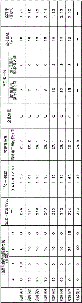
如表1所示,在实施例1~7的带导体层的液晶聚合物膜中,空孔侧重存在于第1位置与第2位置之间,结果是空孔侧重存在于导体层的附近。As shown in Table 1, in the liquid crystal polymer films with conductor layers of Examples 1 to 7, voids mainly existed between the first position and the second position, and as a result, voids mainly existed near the conductor layer.
在实施例1~7的带导体层的液晶聚合物膜中,之所以空孔设置在导体层的附近可认为是因为在制造实施例1~7的带导体层的液晶聚合物膜时使用了粘弹性特性的损耗角正切的积分值为29.7以下的液晶聚合物膜,即,使用了粘弹性特性的损耗角正切的粘性成分少、即使在高温下也不易软化的液晶聚合物膜。可认为,在制造实施例1~7的带导体层的液晶聚合物膜时,由于使用了具有这种特性的液晶聚合物膜,所以在设置上述空孔的工序中,即使对层叠体进行热处理,以设置于液晶聚合物膜的一个主面的凹凸为起点的空间中所含的气体也难以排出到液晶聚合物膜的外部。结果,可认为在实施例1~7的带导体层的液晶聚合物膜中,空间中所含的气体容易进入到液晶聚合物膜的内部,因此容易在液晶聚合物膜的内部、更具体而言在导体层的附近设置空孔。In the liquid crystal polymer films with conductor layers of Examples 1 to 7, the reason why the voids are arranged near the conductor layers is considered to be because the liquid crystal polymer films with conductor layers of Examples 1 to 7 were produced using The integral value of loss tangent of viscoelastic properties is 29.7 or less, that is, a liquid crystal polymer film having less viscous component of loss tangent of viscoelastic properties and hardly softening even at high temperature is used. It is considered that since liquid crystal polymer films having such characteristics are used in the production of the liquid crystal polymer films with conductor layers in Examples 1 to 7, even if the laminate is heat-treated in the step of providing the above-mentioned voids, Therefore, the gas contained in the space starting from the unevenness provided on one main surface of the liquid crystal polymer film is also difficult to be discharged to the outside of the liquid crystal polymer film. As a result, it can be considered that in the liquid crystal polymer films with conductor layers of Examples 1 to 7, the gas contained in the space easily enters the inside of the liquid crystal polymer film, so it is easy to enter the liquid crystal polymer film inside, more specifically, the liquid crystal polymer film. It is said that holes are provided in the vicinity of the conductor layer.
实施例4~7的带导体层的液晶聚合物膜与实施例2和实施例3的带导体层的液晶聚合物膜相比,第1位置与第2位置之间的空孔数和空孔率高。可认为这是因为,在制造实施例4~7的带导体层的液晶聚合物膜时,使用了设置有导体层的一侧的主面的算术平均高度Sa为240nm以上的液晶聚合物膜。Compared with the liquid crystal polymer films with a conductor layer of Examples 4 to 7 and the liquid crystal polymer films with a conductor layer of Examples 2 and 3, the number of pores and the number of pores between the first position and the second position High rate. This is considered to be because liquid crystal polymer films having an arithmetic mean height Sa of the main surface on the side where the conductor layer is provided were 240 nm or more were used when producing the liquid crystal polymer films with conductor layers in Examples 4 to 7.
另一方面,在比较例1的带导体层的液晶聚合物膜中,在液晶聚合物膜的内部不存在空孔。On the other hand, in the liquid crystal polymer film with a conductor layer of Comparative Example 1, voids did not exist inside the liquid crystal polymer film.
在比较例1的带导体层的液晶聚合物膜中,之所以在液晶聚合物膜的内部未设置空孔可认为是因为在制造比较例1的带导体层的液晶聚合物膜时使用了粘弹性特性中的损耗角正切的积分值不为29.7以下的液晶聚合物膜,即,使用了粘弹性特性的损耗角正切的粘性成分多、在高温下容易软化的液晶聚合物膜。可认为,在制造比较例1的带导体层的液晶聚合物膜时,由于使用了具有这种特性的液晶聚合物膜,所以在设置上述空孔的工序中,如果对层叠体进行热处理,则难以维持设置于液晶聚合物膜的一个主面的凹凸的形状,以该凹凸为起点的空间中所含的气体容易排出到液晶聚合物膜的外部。结果,可认为在比较例1的带导体层的液晶聚合物膜中,空间中所含的气体难以进入到液晶聚合物膜的内部,因此在液晶聚合物膜的内部未设置空孔。In the liquid crystal polymer film with a conductor layer of Comparative Example 1, the reason why no voids are provided inside the liquid crystal polymer film is considered to be that an adhesive was used to manufacture the liquid crystal polymer film with a conductor layer of Comparative Example 1. A liquid crystal polymer film whose integral value of loss tangent in elastic properties is not less than 29.7, that is, a liquid crystal polymer film in which the loss tangent of viscoelastic properties has many viscous components and is easily softened at high temperature is used. It is considered that since a liquid crystal polymer film having such characteristics is used in the manufacture of the liquid crystal polymer film with a conductor layer in Comparative Example 1, if the laminate is heat-treated in the step of providing the above-mentioned voids, then It is difficult to maintain the shape of the unevenness provided on one main surface of the liquid crystal polymer film, and the gas contained in the space starting from the unevenness is easily discharged to the outside of the liquid crystal polymer film. As a result, in the liquid crystal polymer film with a conductor layer of Comparative Example 1, it is considered that the gas contained in the space hardly penetrates into the liquid crystal polymer film, and therefore no voids are provided in the liquid crystal polymer film.
附图标记说明Explanation of reference signs
1、1’、1”、1A、1B、1C 树脂膜1, 1’, 1”, 1A, 1B, 1C resin film
1a、1a”、1Aa、1Ba、1Ca 树脂膜的第1主面1a, 1a", 1Aa, 1Ba, 1Ca The first main surface of the resin film
1b、1b”、1Ab、1Bb、1Cb 树脂膜的第2主面1b, 1b", 1Ab, 1Bb, 1Cb The second main surface of the resin film
1h、1h”、1Ah、1Bh、1Ch 空孔1h, 1h”, 1Ah, 1Bh, 1Ch empty hole
2、2’、2”、2A、2B、2B’、2B”、2C 导体层2, 2’, 2”, 2A, 2B, 2B’, 2B”, 2C conductor layer
10、10’、10”、10A、10B、10C 带导体层的树脂膜10, 10’, 10”, 10A, 10B, 10C Resin film with conductor layer
15 层叠体15 stacks
15h 空间15h space
20A、20B、20C、20D 层间连接导体20A, 20B, 20C, 20D Interlayer connection conductors
21A、21B、21C、21D 通孔21A, 21B, 21C, 21D Through holes
22A、22B、22C、22D 导电性糊剂22A, 22B, 22C, 22D Conductive Paste
30 侧面导体30 side conductor
50、50’、50A、50A’、50B 层叠基板50, 50’, 50A, 50A’, 50B laminated substrates
E1、E1”、EA1、EB1、EC1 第1位置E1, E1", EA1, EB1, EC1 1st position
E2、E2”、EA2、EB2、EC2 第2位置E2, E2", EA2, EB2, EC2 2nd position
E3、E3”、EA3、EB3、EC3 第3位置E3, E3", EA3, EB3, EC3 3rd position
HD 厚度方向HD thickness direction
MD 第1方向MD 1st direction
TD 第2方向。TD 2nd direction.
Claims (11)
Applications Claiming Priority (3)
| Application Number | Priority Date | Filing Date | Title |
|---|---|---|---|
| JP2021-096549 | 2021-06-09 | ||
| JP2021096549 | 2021-06-09 | ||
| PCT/JP2022/023160 WO2022260094A1 (en) | 2021-06-09 | 2022-06-08 | Conductor-layer-coated resin film, layered substrate, and method for producing conductor-layer-coated resin film |
Publications (1)
| Publication Number | Publication Date |
|---|---|
| CN116323184A true CN116323184A (en) | 2023-06-23 |
Family
ID=84426093
Family Applications (2)
| Application Number | Title | Priority Date | Filing Date |
|---|---|---|---|
| CN202280006626.6A Pending CN116323184A (en) | 2021-06-09 | 2022-06-08 | Resin film with conductor layer, laminated substrate, and method for producing resin film with conductor layer |
| CN202280006625.1A Pending CN116249617A (en) | 2021-06-09 | 2022-06-08 | Liquid crystal polymer film, liquid crystal polymer film with conductor layer, and laminated substrate |
Family Applications After (1)
| Application Number | Title | Priority Date | Filing Date |
|---|---|---|---|
| CN202280006625.1A Pending CN116249617A (en) | 2021-06-09 | 2022-06-08 | Liquid crystal polymer film, liquid crystal polymer film with conductor layer, and laminated substrate |
Country Status (4)
| Country | Link |
|---|---|
| US (2) | US12507340B2 (en) |
| JP (2) | JP7722451B2 (en) |
| CN (2) | CN116323184A (en) |
| WO (2) | WO2022260094A1 (en) |
Families Citing this family (8)
| Publication number | Priority date | Publication date | Assignee | Title |
|---|---|---|---|---|
| CN116323184A (en) | 2021-06-09 | 2023-06-23 | 株式会社村田制作所 | Resin film with conductor layer, laminated substrate, and method for producing resin film with conductor layer |
| JP7779915B2 (en) * | 2021-07-20 | 2025-12-03 | 住友電気工業株式会社 | Printed wiring board and method for manufacturing printed wiring board |
| JP2024071004A (en) * | 2022-11-14 | 2024-05-24 | 日東電工株式会社 | LAMINATE AND METHOD FOR MANUFACTURING LAMINATE |
| CN121420631A (en) * | 2023-07-25 | 2026-01-27 | 株式会社村田制作所 | Resin laminated substrate and method for producing resin laminated substrate |
| WO2025169634A1 (en) * | 2024-02-07 | 2025-08-14 | 日東電工株式会社 | Flexible multilayer circuit board |
| TWI859075B (en) * | 2024-02-19 | 2024-10-11 | 欣興電子股份有限公司 | Wiring board structure |
| WO2026014245A1 (en) * | 2024-07-12 | 2026-01-15 | 株式会社村田製作所 | Resin sheet body, resin sheet body equipped with conductor layer, and multilayer circuit board |
| WO2026014243A1 (en) * | 2024-07-12 | 2026-01-15 | 株式会社村田製作所 | Resin sheet body, resin sheet body with conductor layer, multilayer circuit board, and method for manufacturing multilayer circuit board |
Citations (2)
| Publication number | Priority date | Publication date | Assignee | Title |
|---|---|---|---|---|
| JP2003008233A (en) * | 2001-06-19 | 2003-01-10 | Nitto Denko Corp | Multilayer wiring board |
| WO2021059586A1 (en) * | 2019-09-25 | 2021-04-01 | 富士フイルム株式会社 | Liquid crystal polymer film, method for producing same, flexible copper-clad laminate and flexible printed circuit board |
Family Cites Families (18)
| Publication number | Priority date | Publication date | Assignee | Title |
|---|---|---|---|---|
| US5494858A (en) | 1994-06-07 | 1996-02-27 | Texas Instruments Incorporated | Method for forming porous composites as a low dielectric constant layer with varying porosity distribution electronics applications |
| JP2005142473A (en) * | 2003-11-10 | 2005-06-02 | Semiconductor Leading Edge Technologies Inc | Manufacturing method of semiconductor device |
| JP4577715B2 (en) * | 2005-01-05 | 2010-11-10 | 株式会社神戸製鋼所 | Method for manufacturing porous dielectric substrate having pattern electrode |
| CN101223835B (en) | 2005-07-27 | 2012-07-04 | 株式会社可乐丽 | Process for manufacturing circuit board covered with thermoplastic liquid crystal polymer film |
| JP5154055B2 (en) | 2006-10-19 | 2013-02-27 | 株式会社プライマテック | Electronic circuit board manufacturing method |
| JP6530716B2 (en) * | 2013-11-01 | 2019-06-12 | 株式会社クラレ | Method of manufacturing thermoplastic liquid crystal polymer film, circuit board and method of manufacturing the same |
| CN206332152U (en) * | 2014-06-02 | 2017-07-14 | 株式会社村田制作所 | transmission line components |
| JP6135825B2 (en) * | 2014-06-02 | 2017-05-31 | 株式会社村田製作所 | Transmission line member |
| WO2017110618A1 (en) | 2015-12-24 | 2017-06-29 | 株式会社村田製作所 | Resin sheet, method for manufacturing resin sheet, and method for manufacturing multilayer resin substrate |
| JP6854124B2 (en) * | 2016-12-28 | 2021-04-07 | 株式会社クラレ | Thermoplastic liquid crystal polymer film and circuit board using it |
| JP6841287B2 (en) | 2017-02-16 | 2021-03-10 | 株式会社村田製作所 | Multi-layer board |
| KR20210028607A (en) * | 2018-07-10 | 2021-03-12 | 덴카 주식회사 | Thermoplastic liquid crystal polymer film, its manufacturing method and flexible copper clad laminate |
| KR102518009B1 (en) * | 2019-04-23 | 2023-04-04 | 주식회사 쿠라레 | Thermoplastic liquid crystal polymer films, laminates, molded articles, and methods for producing them |
| CN116261519B (en) | 2020-09-30 | 2025-09-19 | 大金工业株式会社 | Fluororesin material, laminate, tube, and method for producing tube |
| TW202229426A (en) | 2020-09-30 | 2022-08-01 | 日商富士軟片股份有限公司 | Liquid crystal polymer film, flexible copper clad laminate, and method for producing liquid crystal polymer film |
| JP7327690B2 (en) | 2020-11-30 | 2023-08-16 | 株式会社村田製作所 | Transmission lines and electronic equipment |
| JP2022086176A (en) * | 2020-11-30 | 2022-06-09 | 東レ株式会社 | Liquid crystalline polyester resin composition, laminate, method for producing the same and liquid crystalline polyester resin film |
| CN116323184A (en) | 2021-06-09 | 2023-06-23 | 株式会社村田制作所 | Resin film with conductor layer, laminated substrate, and method for producing resin film with conductor layer |
-
2022
- 2022-06-08 CN CN202280006626.6A patent/CN116323184A/en active Pending
- 2022-06-08 JP JP2023527903A patent/JP7722451B2/en active Active
- 2022-06-08 CN CN202280006625.1A patent/CN116249617A/en active Pending
- 2022-06-08 WO PCT/JP2022/023160 patent/WO2022260094A1/en not_active Ceased
- 2022-06-08 WO PCT/JP2022/023153 patent/WO2022260092A1/en not_active Ceased
- 2022-06-08 JP JP2023527901A patent/JPWO2022260092A1/ja active Pending
-
2023
- 2023-03-31 US US18/193,696 patent/US12507340B2/en active Active
- 2023-03-31 US US18/193,703 patent/US12330392B2/en active Active
Patent Citations (2)
| Publication number | Priority date | Publication date | Assignee | Title |
|---|---|---|---|---|
| JP2003008233A (en) * | 2001-06-19 | 2003-01-10 | Nitto Denko Corp | Multilayer wiring board |
| WO2021059586A1 (en) * | 2019-09-25 | 2021-04-01 | 富士フイルム株式会社 | Liquid crystal polymer film, method for producing same, flexible copper-clad laminate and flexible printed circuit board |
Also Published As
| Publication number | Publication date |
|---|---|
| US12507340B2 (en) | 2025-12-23 |
| US20240076552A9 (en) | 2024-03-07 |
| JPWO2022260094A1 (en) | 2022-12-15 |
| JPWO2022260092A1 (en) | 2022-12-15 |
| JP7722451B2 (en) | 2025-08-13 |
| US12330392B2 (en) | 2025-06-17 |
| US20230262876A1 (en) | 2023-08-17 |
| CN116249617A (en) | 2023-06-09 |
| WO2022260094A1 (en) | 2022-12-15 |
| WO2022260092A1 (en) | 2022-12-15 |
| US20230235229A1 (en) | 2023-07-27 |
Similar Documents
| Publication | Publication Date | Title |
|---|---|---|
| CN116323184A (en) | Resin film with conductor layer, laminated substrate, and method for producing resin film with conductor layer | |
| CN103404239B (en) | Multi-layered wiring board and manufacture method thereof | |
| JP6337909B2 (en) | Manufacturing method of electronic component module | |
| CN116724075B (en) | Porous liquid crystal polymer sheet, porous liquid crystal polymer sheet with metal layer, and electronic circuit board | |
| TW200920196A (en) | Wiring substrate and method of manufacturing the same | |
| US12167545B2 (en) | Multilayer substrate | |
| US12503649B2 (en) | Porous liquid crystal polymer sheet, metal layer-attached porous liquid crystal polymer sheet, and electronic circuit board | |
| TW201715921A (en) | Insulating colloidal material and multilayer circuit structure | |
| WO2012117478A1 (en) | Metal junction structure and metal junction method | |
| JP2014110282A (en) | Bonding method using paste containing metal fine particle | |
| TW540281B (en) | Manufacturing method of conductive paste material and manufacturing method of printing wiring base board | |
| US11546989B2 (en) | Multilayer board insulating sheet, multilayer board, and method of manufacturing multilayer board | |
| CN220785102U (en) | Laminated substrate and antenna substrate | |
| JP2004111701A (en) | Printed wiring board and its manufacturing method | |
| CN103824786B (en) | A kind of thick gold wire bonding method | |
| CN119183468A (en) | Resin composition, resin sheet, resin sheet with conductor layer, laminated substrate, and method for producing resin sheet | |
| US11445605B2 (en) | Printed wiring board, multilayer printed wiring board and method for manufacturing printed wiring board | |
| WO2025134700A1 (en) | Laminated substrate | |
| WO2022118658A1 (en) | Laminated substrate | |
| JP2024156373A (en) | Wiring board and manufacturing method thereof | |
| TWI307259B (en) | Manufacturing method of copper clad laminate for via on pad |
Legal Events
| Date | Code | Title | Description |
|---|---|---|---|
| PB01 | Publication | ||
| PB01 | Publication | ||
| SE01 | Entry into force of request for substantive examination | ||
| SE01 | Entry into force of request for substantive examination |